Embed Size (px)
Citation preview
ECE 663
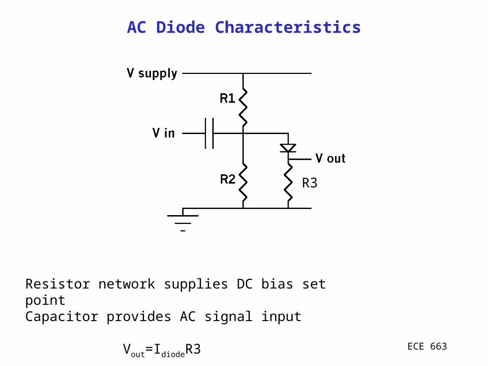
AC Diode Characteristics
Resistor network supplies DC bias set pointCapacitor provides AC signal input
Vout=IdiodeR3
R3

ECE 663
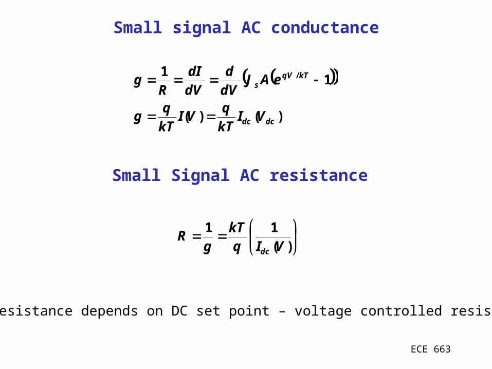
AC small signal resistance
ECE 663
Small signal AC conductance
)()(
11 /
dcdc
kTqVs
VIkTq
VIkTq
g
eAJdVd
dVdI
Rg
Small Signal AC resistance
)(11VIq
kTg
Rdc
Resistance depends on DC set point – voltage controlled resistor
ECE 663
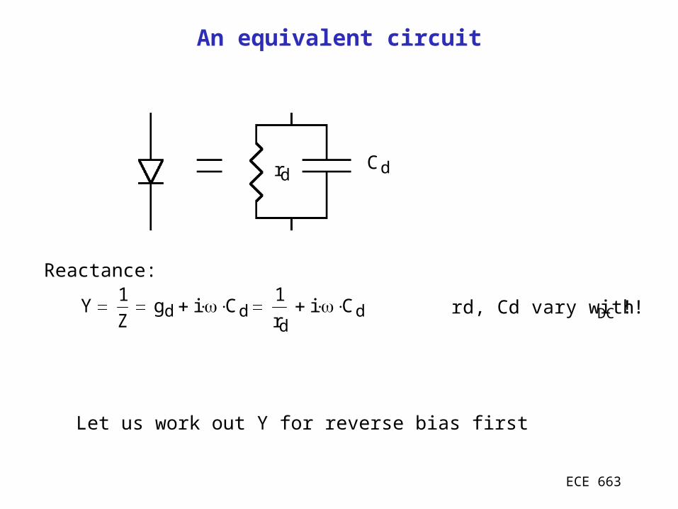
Cdrd
Y1
Zgd i Cd 1
rdi Cd rd, Cd vary with VDC !!!
Reactance:
An equivalent circuit
Let us work out Y for reverse bias first
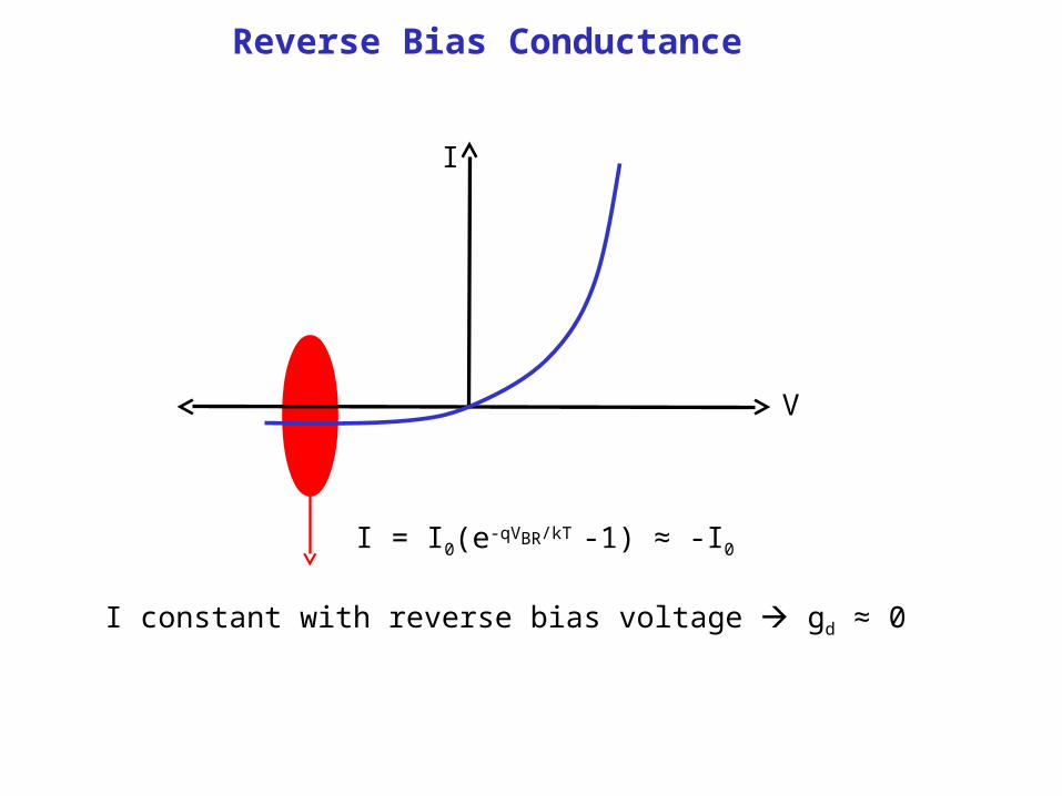
Reverse Bias Conductance
I
V
I constant with reverse bias voltage gd ≈ 0
I = I0(e-qVBR/kT -1) ≈ -I0
ECE 663
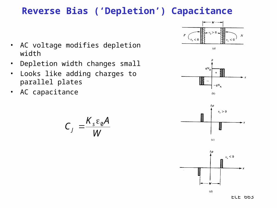
Reverse Bias (‘Depletion’) Capacitance
• AC voltage modifies depletion width• Depletion width changes small• Looks like adding charges to parallel
plates• AC capacitance
WAK
C sJ
0
ECE 663
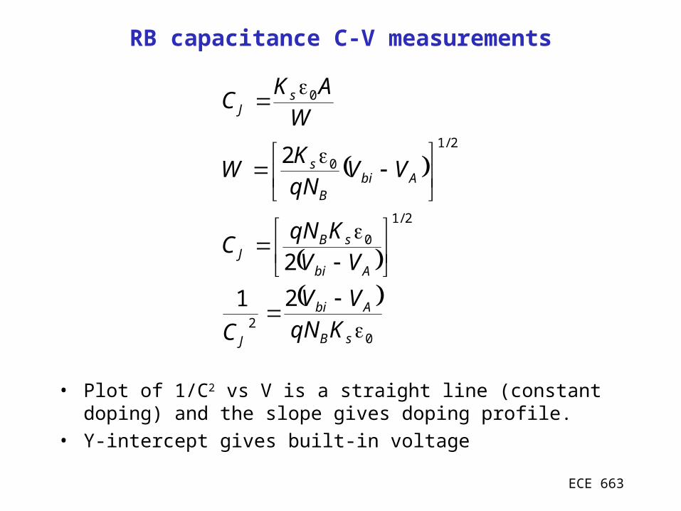
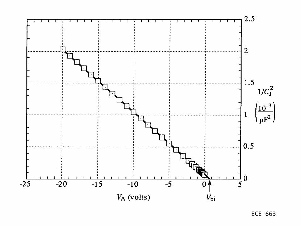
RB capacitance C-V measurements
• Plot of 1/C2 vs V is a straight line (constant doping) and the slope gives doping profile.
• Y-intercept gives built-in voltage
02
2/1
0
2/1
0
0
21
2
2
sB
Abi
J
Abi
sBJ
AbiB
s
sJ
KqNVV
C
VVKqN
C
VVqNK
W
WAK
C
ECE 663
ECE 663
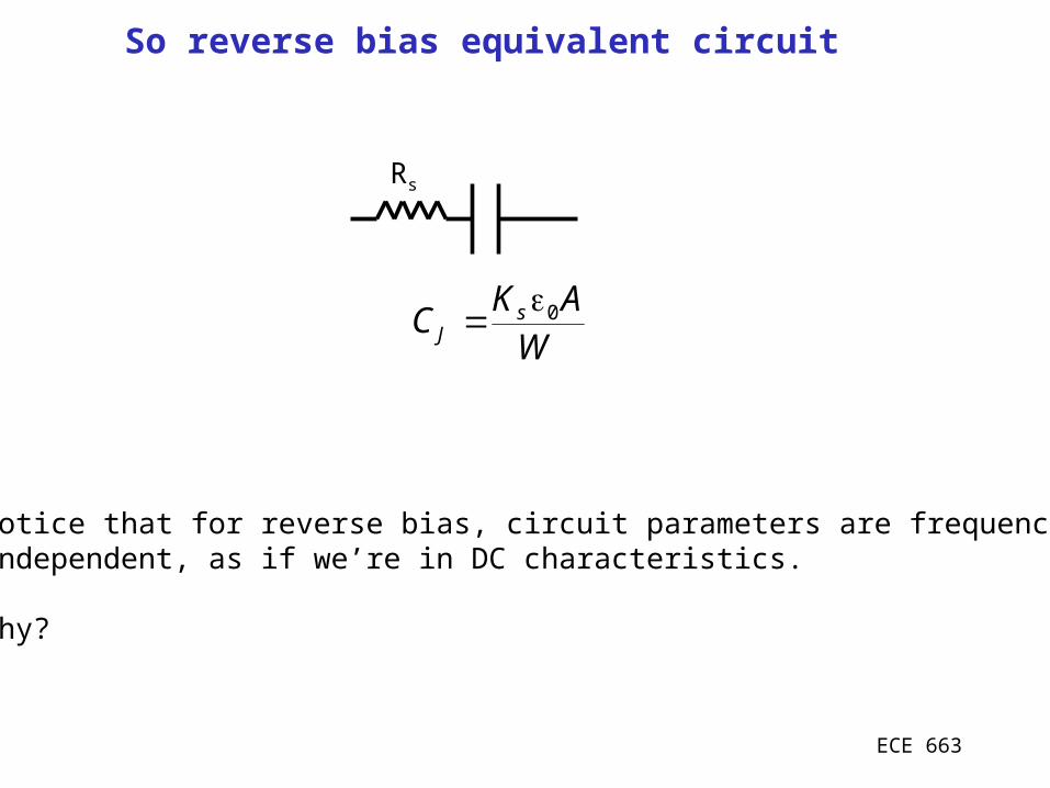
So reverse bias equivalent circuit
WAK
C sJ
0
Rs
Notice that for reverse bias, circuit parameters are frequencyindependent, as if we’re in DC characteristics.
Why?
ECE 663
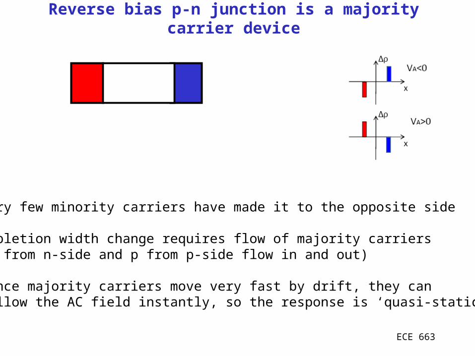
Reverse bias p-n junction is a majority carrier device
Very few minority carriers have made it to the opposite side
Depletion width change requires flow of majority carriers(n from n-side and p from p-side flow in and out)
Since majority carriers move very fast by drift, they can follow the AC field instantly, so the response is ‘quasi-static’
ECE 663
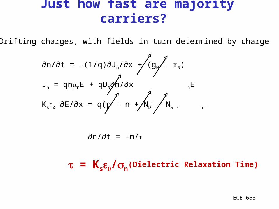
Just how fast are majority carriers?
Drifting charges, with fields in turn determined by charge
∂n/∂t = -(1/q)∂Jn/∂x + (gN - rN)
Jn = qnnE + qDN∂n/∂x ≈ qnnE ≈ nE
Ks0 ∂E/∂x = q(p - n + ND+ - NA
-) ≈ -qn
∂n/∂t = -n/
= Ks/n(Dielectric Relaxation Time)
ECE 663
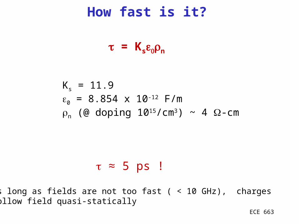
How fast is it?
= Ksn
Ks = 11.90 = 8.854 x 10⁻¹² F/mn (@ doping 1015/cm3) ~ 4 -cm
≈ 5 ps !
As long as fields are not too fast ( < 10 GHz), chargesfollow field quasi-statically

ECE 663
Let’s now go to forward bias
ECE 663
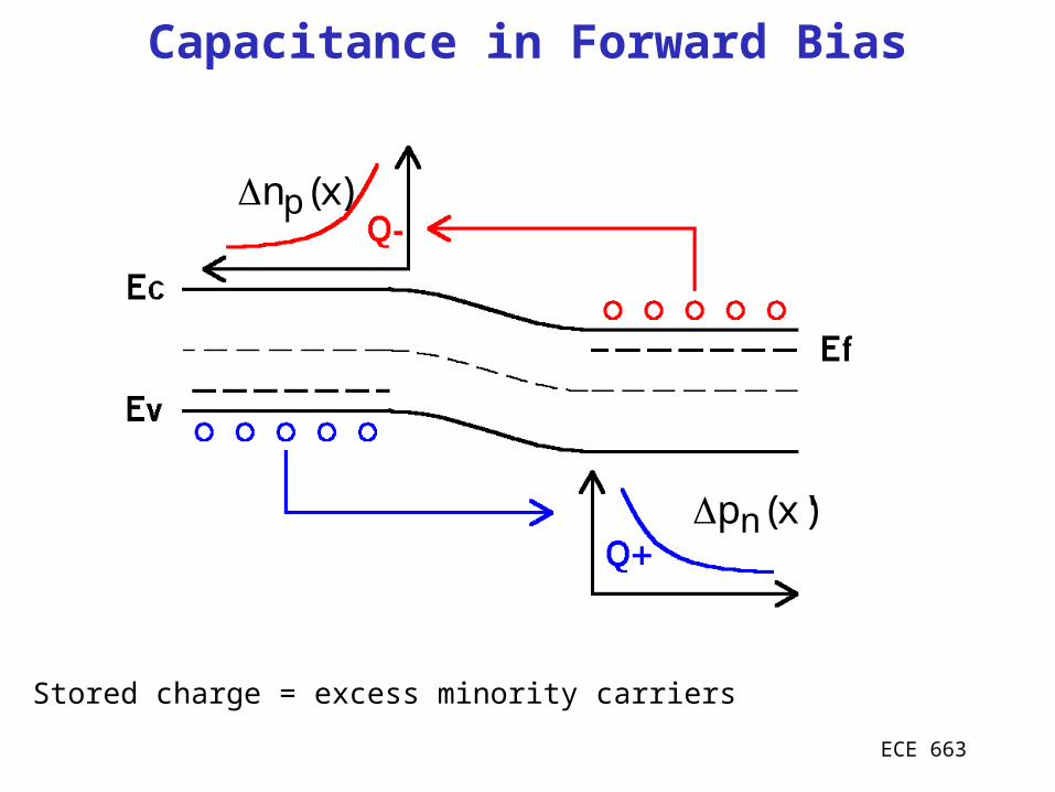
Capacitance in Forward Bias
np x( )
pn x'( )
Stored charge = excess minority carriers
ECE 663
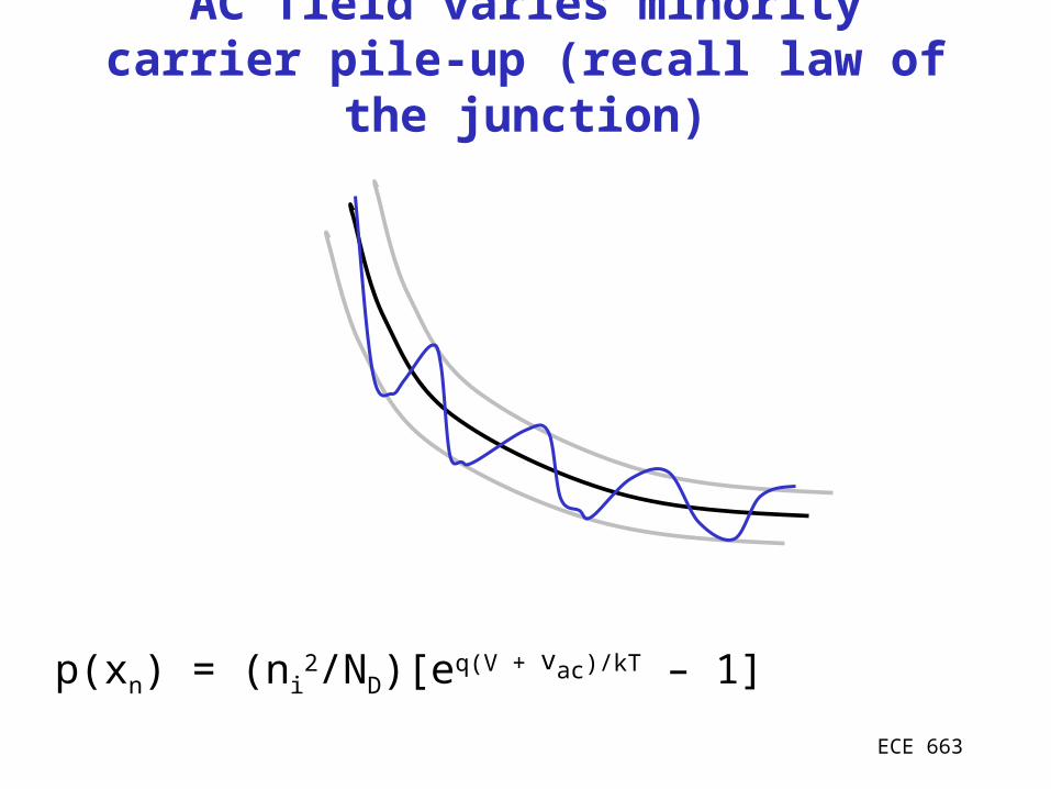
AC field varies minority carrier pile-up (recall law of the
junction)
p(xn) = (ni2/ND)[eq(V + vac)/kT – 1]
ECE 663
Also, minority carriers are slow and may not follow AC field quasi-
statically
Thus we expect circuit parametersto be frequency-dependent !

ECE 663
How fast are minority carriers?
≈ 1/NTTvt (Minority carrier lifetime)
NT ~ 1012/cm3 (for NA ~ 1014/cm3)T ~ (10-10m)3
vt = 3kT/m ~ 105m/s
≈ 300 s
So for fast fields ( >> 1/), expect carriers to go out of phase, leading tofreq-dependent circuit parameters
ECE 663
But how do we include such phase lag effects?
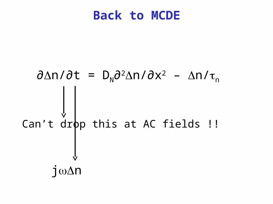
Back to MCDE
∂n/∂t = DN∂2n/∂x2 – n/n
Can’t drop this at AC fields !!
jn
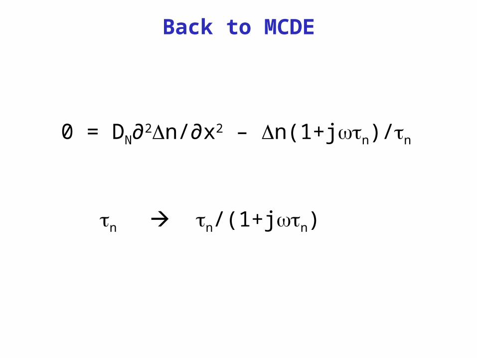
Back to MCDE
0 = DN∂2n/∂x2 – n(1+jn)/n
n n/(1+jn)

So in Shockley equation
I = qA(ni2/ND)DN (1+jn)
/n
x [eq(V + vac)/kT – 1] idiff = G0(1+jn)vac
idiff = (Gd + jCd)vac

Square root of (1+jn)
1 + j = Aej
A = (1 + 22) = tan-1()
Real(1+j) = A1/2cos(/2)
Im(1+j) = A1/2sin(/2)
cos = 1/(1+22) = 2cos2(/2) - 1 = 1 – 2sin2(/2)
Re(1+j) = Gd
Im(1+j) = jCd
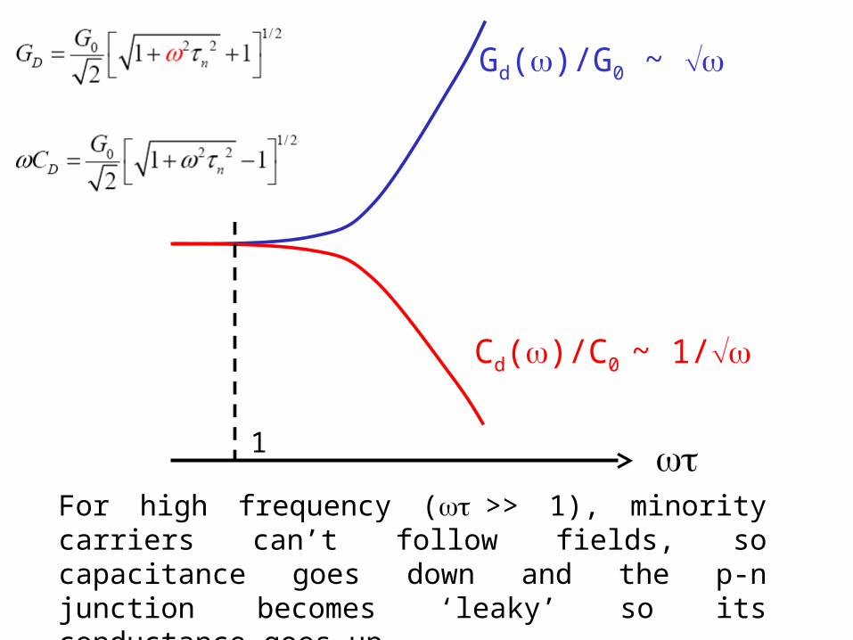
1
Gd()/G0 ~
Cd()/C0 ~ 1/
For high frequency (>> 1), minority carriers can’t follow fields, so capacitance goes down and the p-n junction becomes ‘leaky’ so its conductance goes up
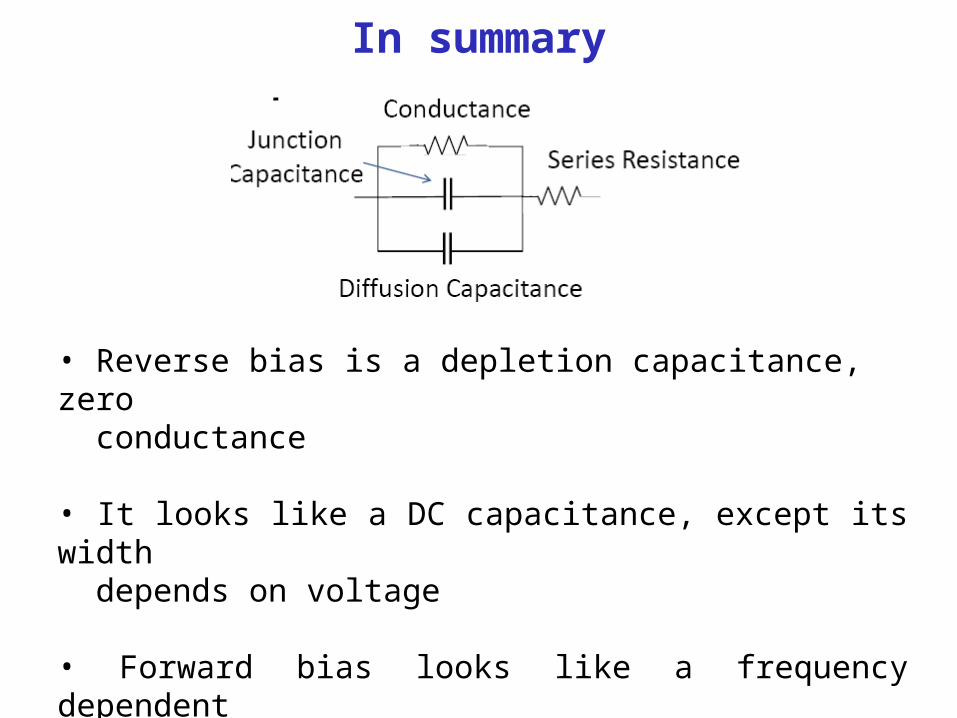
In summary
• Reverse bias is a depletion capacitance, zero conductance
• It looks like a DC capacitance, except its width depends on voltage
• Forward bias looks like a frequency dependent diffusion capacitance and a diffusion conductance to give an overall admittance


![Datasheet Filter Diode AC/DC コンバータ IC スイッ …...Datasheet Filter Diode AC/DC コンバータ IC スイッチング ... ... 0)]]]]]](https://img.dokumen.tips/doc/110x75/5e2b488407a13006d8628ca3/datasheet-filter-diode-acdc-fff-ic-ff-datasheet-filter-diode.jpg)