Embed Size (px)
Citation preview
class notes, M. Rodwell, copyrighted 2013
ECE 2C, notes set 4: Transistor Amplifiers ...basic considerations
Mark Rodwell
University of California, Santa Barbara
[email protected] 805-893-3244, 805-893-3262 fax
class notes, M. Rodwell, copyrighted 2013
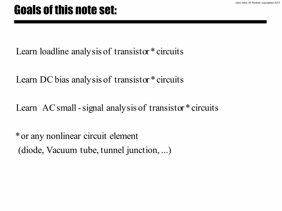
Goals of this note set:
...) junction, tunnel tube,Vacuum (diode,
elementcircuit nonlinear any or *
circuits *r transistoof analysis signal-small ACLearn
circuits *r transistoof analysis bias DCLearn
circuits *r transistoof analysis loadlineLearn
class notes, M. Rodwell, copyrighted 2013
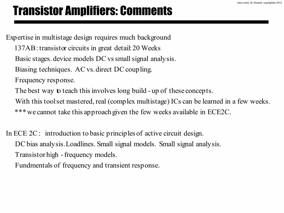
Transistor Amplifiers: Comments
response. transientandfrequency of sFundmental
models.frequency -high Transistor
analysis. signal Small models. signal Small Loadlines. analysis. bias DC
design.circuit active of principles basic on tointroducti :2C ECEIn
ECE2C.in available weeksfew given theapproach thisecannot tak we***
weeks.few ain learned becan ICs )multistage(complex real mastered,set toolthis With
concepts. theseof up-build long involves s teach thiobest way t The
response.Frequency
coupling. DCdirect vs.AC s. techniqueBiasing
analysis. signal small vsDC models device stages. Basic
Weeks20 :detailgreat in circuitsr transisto:137AB
backgroundmuch requiresdesign multistagein Expertise
class notes, M. Rodwell, copyrighted 2013
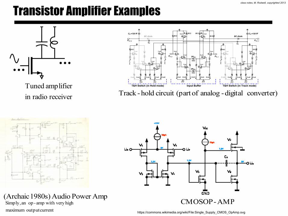
Transistor Amplifier Examples
receiver radioin
amplifier Tuned
AmpPower Audio 1980s) (Archaic
converter) digital-analog of(part circuit hold-Track
https://commons.wikimedia.org/wiki/File:Single_Supply_CMOS_OpAmp.svg
AMP-OP CMOScurrentoutput maximum
high with veryamp-opan Simply,
class notes, M. Rodwell, copyrighted 2013
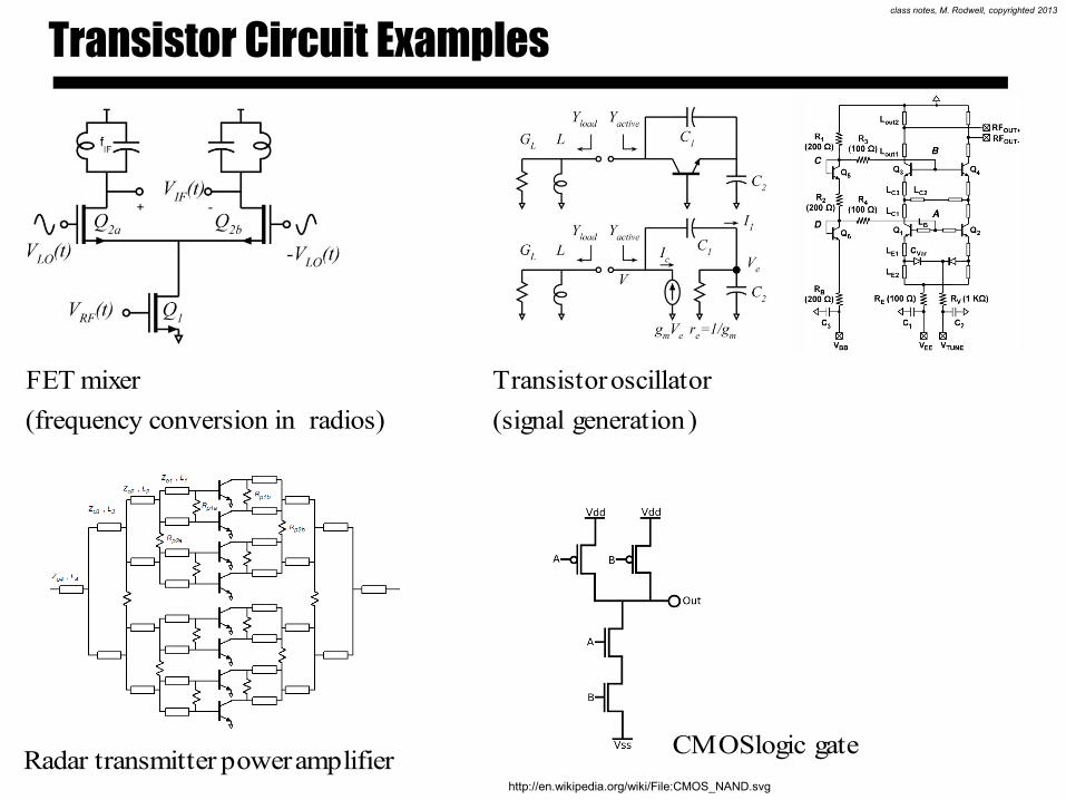
Transistor Circuit Examples
radios)in conversion (frequency
mixer FET
)generation (signal
oscillator Transistor
amplifierpower smitter Radar tranhttp://en.wikipedia.org/wiki/File:CMOS_NAND.svg
gate logic CMOS

class notes, M. Rodwell, copyrighted 2013
Elementary Common-Source Amplifier
analysis step-by-step :First
output. on the appears signal amplifiedAn
applied. is signalinput An
network bias DC a and supply,power a load, a r, transistoa isamplifier The

class notes, M. Rodwell, copyrighted 2013
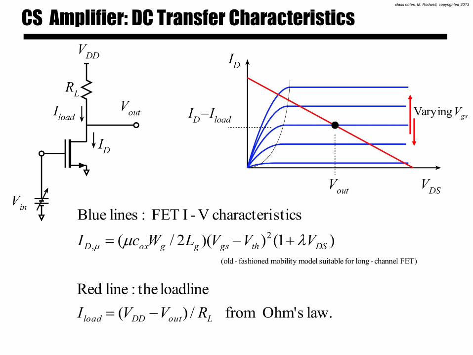
CS Amplifier: DC Transfer Characteristics
inout VV offunction a as compute usLet
class notes, M. Rodwell, copyrighted 2013
CS Amplifier: DC Transfer Characteristics
)1())(2/(
sticscharacteri V-I FET :lines Blue
2
, DSthgsggoxD VVVLWcI
gsV Varying
law. sOhm' from /)(
loadline the:line Red
LoutDDload RVVI
FET) channel-longfor suitable modelmobility fashioned-old(
class notes, M. Rodwell, copyrighted 2013
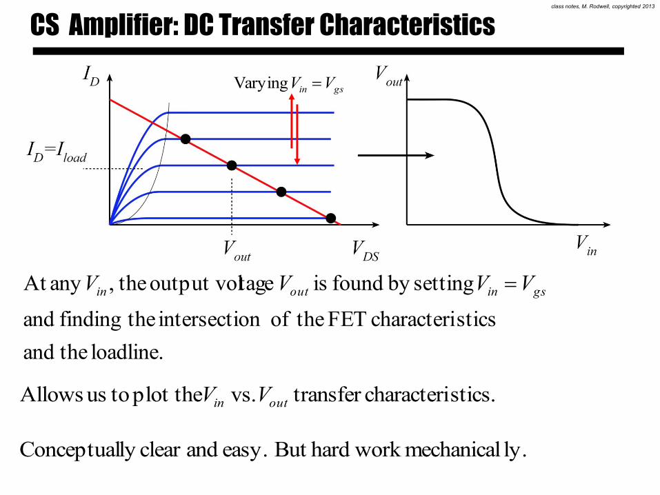
CS Amplifier: DC Transfer Characteristics
loadline. theand
sticscharacteri FET theofon intersecti thefinding and
settingby found is tageoutput vol the,any At gsinoutin VVVV
stics.characteri transfer vs. plot the tous Allows outin VV
ly.mechanical work hardBut easy. andclear ly Conceptual
gsin VV Varying
class notes, M. Rodwell, copyrighted 2013
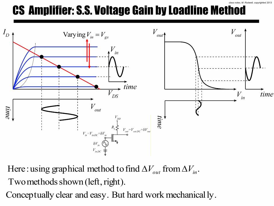
CS Amplifier: S.S. Voltage Gain by Loadline Method
. from find tomethod graphical using :Here inout VV
ly.mechanical work hardBut easy. andclear ly Conceptual
right). (left,shown methods Two
gsin VV Varying
class notes, M. Rodwell, copyrighted 2013
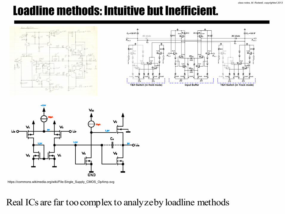
Loadline methods: Intuitive but Inefficient.
methods loadlineby analyze complex to far too are ICs Real
https://commons.wikimedia.org/wiki/File:Single_Supply_CMOS_OpAmp.svg

class notes, M. Rodwell, copyrighted 2013
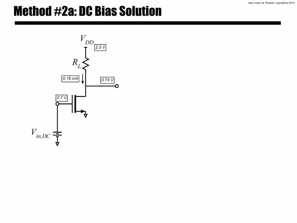
Method #2a: Finding the DC Bias Conditions
mA 16.0)1()3.07.0)(mA/V 1(
)1())(2/(
:Analysis
22
2
DS
DSthgsggoxD
VVV
VVVLWcI
V10/1
V 3.0
mA/V1)2/(
:FET
2
th
ggox
V
LWc
:Parameters Example
V 7.0
k 1.1
V 5.2
Circuit
,
DCin
L
dd
V
R
V
*ignore
analysis. signal small
in the term)1( theignorenot Do
.accuratelyfairly yet quickly thiscalculate
to trickssomelearn willECE137A weIn
Hard. formulas. quadratic
solving involves analysis DC thenot, do weIf
error. small some causes thisDoing
analysis. bias
in the term)1( theignoring are we*
DS
DS
V
V
V. 74.0
m)mA)(1.1kOh16.0( 2.5V
,
LDDDDCout RIVV
class notes, M. Rodwell, copyrighted 2013
Method #2a: DC Bias Solution
class notes, M. Rodwell, copyrighted 2013
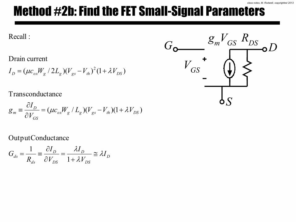
Method #2b: Find the FET Small-Signal Parameters
RDS
gmVGS
VGS
D
S
G
D
DS
D
DS
D
ds
ds
DSthgsggox
GS
Dm
DSthgsggoxD
IV
I
V
I
RG
VVVLWcV
Ig
VVVLWcI
1
1
eConductancOutput
)1)()(/(
ctanceTranscondu
)1())(2/(
currentDrain
:Recall
2

class notes, M. Rodwell, copyrighted 2013
Method #2b: Find the FET Small-Signal Parameters
RDS
gmVGS
VGS
D
S
G
62.5k
1S 16
10V
mA16.01
mS 0.856
)V/10V74.01)(V3.0V7.0)(mA/V2(
)1)()(/(
:Analysis
2
D
ds
ds
DSthgsggoxm
IR
G
VVVLWcg
V10/1
V 3.0
mA/V1)2/(
:FET
2
th
ggox
V
LWc
:Parameters Example
mA 16.0
V 7.0
V 7.0
conditions Bias
D
DS
gs
I
V
V
class notes, M. Rodwell, copyrighted 2013
Method #2c: Find the Small-Signal Equivalent Circuit
oltage.constant v afor 0 Because
circuits-short with
voltagessupply) & (biasconstant Replaced 2)
model signal-small its
r with transisto theReplace 1)
circuit In this
V
inVoutV
signals. small are that these
implicit as taken isit
:droppedbeen has
notation "" The
circuit. equivalent
signal-small theis This
V

class notes, M. Rodwell, copyrighted 2013
Method #2c: Find the small-signal gain
8.0- ofgain voltagea hascircuit The
0.8
)k 35.9mS)(856.0(
:law sOhm' From
k 35.9
1k1||k5.62||
resistance load equivalent
:Analysis
,
Leqm
in
out
ininLeqmout
DSLeqL
RgV
V
VVRgV
RRR
k 5.62
mS 856.0
:FET
DS
m
R
g
:Parameters Example
k 11
Circuit
LR
class notes, M. Rodwell, copyrighted 2013
Comments
4.-1on focus will weECE2C,In
etc. voltage,signal maximum find tohinqueother tec use 5)
interest). of parametersother gain, voltagefind (to analyze 4)
circuit equivalent signal smallcircuit active draw 3)
models signal smallr transistofind 2)
math)by ( conditions bias DC Find 1)
:analysiscircuit Active
stics)characteri transfer gate logic ,amplifierspower :(except
circuits. sophomore outside usedrarely are...but
tool... teachinggood a are Loadlines

class notes, M. Rodwell, copyrighted 2013
Example: Complementary MOS (CMOS) Amplifier
V. 5.0 :Bias
V 0.1 :Supply
)V10/1()V3.0)(mA/V 1( : *sticscharacteri V-I FET
,
22
DCin
DD
DSgsD
V
V
VVI
FET-P for the needed changessign ignoring FETs,both For *

class notes, M. Rodwell, copyrighted 2013
CMOS Amplifier: Graphical DC Bias Analysis
PFETDNFETD II ,,
DCinNFETgs VV ,,
DCinDDPFETgs VVV ,,
DCoutNFETDS VV ,,
DCoutDDPFETds VVV ,,
graph single aon ipsrelationsh theserepresent :Next
sticscharacteri NFET
sticscharacteri PFET

class notes, M. Rodwell, copyrighted 2013
CMOS Amplifier: Graphical DC Bias Analysis
graph single aon
ipsrelationsh theseRepresent
work.hard isit but
clear, is procedure theagain, Once
. versus ofplot a
thisfrom makecan we...and
outin VV
Volts. 5.0
when Volts 5.0
thatfound have we:Note
in
out
V
V

class notes, M. Rodwell, copyrighted 2013
CMOS Amplifier: FET Small-Signal Parameters
:Parameters Example
V10/1
V 3.0
mA/V1)2/(
:FET
2
th
ggox
V
LWc
V 5.0
V 5.0
conditions Bias
DS
gs
V
V
250k
1S 0.4
10V
A 041
A.40)V3.0V5.0)(mA/V2(
) term theskip())(2/(
mS 0.42
)V/10V5.01)(V3.0V5.0)(mA/V2(
)1)()(/(
:FETs)both for parameters (same Analysis
22
2
2
D
ds
ds
DSthgsggoxD
DSthgsggoxm
IR
G
VVVLWcI
VVVLWcg

class notes, M. Rodwell, copyrighted 2013
CMOS Amplifier: Small-Signal Equivalent Circuit
circuits.open with
sourcescurrent DC Replace
circuits.-short with sources
DC andsupply Power Replace
model. SSwith
symbol FET replacingwhen
G-G D,-D S,-Sconnect :careful Be
model. signal smallit with
FETeach Replace
:Steps
class notes, M. Rodwell, copyrighted 2013
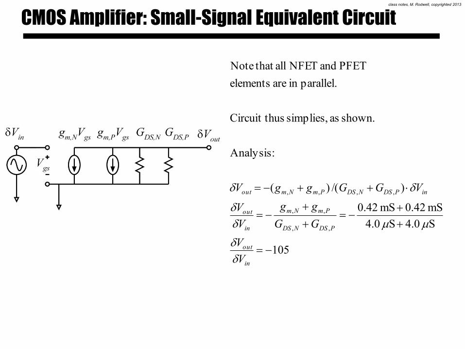
CMOS Amplifier: Small-Signal Equivalent Circuit
105
S 0.4S 0.4
mS 42.0mS 42.0
)/()(
:Analysis
shown. as simplies, usCircuit th
parallel.in are elements
PFET and TNFE all that Note
,,
,,
,,,,
in
out
PDSNDS
PmNm
in
out
inPDSNDSPmNmout
V
V
GG
gg
V
V
VGGggV