Embed Size (px)
Citation preview

1
課程名稱:微製造技術Microfabrication Technology
授課教師:王東安Lecture 6Etching

2
Lecture Outline
•Reading Campbell: Chapter 11•Today’s lecture
–Wet etching–Chemical mechanical polishing–Plasma etching–Ion milling–Reactive ion etching–High-density plasma etching–Liftoff

3
Prologue
•After resist formed, developed, next transferimage into substrate by etching.
•Wet etching: wafer is immersed in a solutionthat reacts with the exposed film to formsoluable by-products.
•Wet etching is prone to defect–Solution particulate contamination–Not for small feature–Large volume of chemical waste

4
Figure of Merit•Etch rate•Uniformity
–Etch rate variation over awafer
–Etch rate variation from waferto wafer
•Selectivity•Undercut•Etch rate anisotropy
A = 1 –RL/RV
RL: lateral etch rateRV: vertical etch rate
•A=1 perfectly anisotropic•A=0 perfectly isotropic

5
Range of etch process•Ion milling: energetic beam in very low
pressure, mean free path of ions is muchlonger than chamber diameter therefore highdegree of anisotropy
•Wet etching: low anisotropy, high selectivity

6
Wet etching•Drawback:
–Lack of anisotropy–Poor process control–Particle contamination
•Pro–Highly selective–Does not damage substrate

7
Wet etching•Consists of 3 processes
–Movement of etchant species to wafer surface–Chemical reaction with exposed film that produces soluble
by-products–Movement of reaction products away from wafer surface
•Wet etch solution is often agitated to assist movementof etchant to surface and removal of etch product
•Some wet etch use a acid spray to supply freshetchant
•Small geometry features may etch more slowly, dueto difficulty in removing etch products

8
Wet etching•Undected resist scumming: when exposed
resist is not removed in develop process•Scum: A filmy layer of extraneous or impure
matter that forms on or rises to the surface of aliquid or body of water

9
HF Wet etching of SiO2•Wet etching of SiO2 in dilute solutions of
hydrofluoric acid: etchants are 6:1, 10:1, 20:1,meaning 6, 10, 20 parts (by volume) of waterto one part of HF. It is isotropic.
•HF solutions are extremely selective of oxideover silicon, some etching of Si occurs sincewater will oxidize Si surface and HF will etchthis oxide.

10
HF Wet etching of SiO2•SiO2+6HF -> H2+SiF6+2H2O•This reaction consumes HF, reaction rate
decrease with time•To avoid that, use HF with a buffering agent
(BHF) such as ammonium fluoride (NH4F),which maintains a constant concentration ofHF through dissolution reactionNH4F <-> NH3+HFwhere NH3 (ammonia) is a gas. Buffering alsocontrols etchant PH, which minimizes resistattack.

11
Silicon nitride etching•H3PO4 at 140-200℃•3:10 of 49% HF (in H2O) and 70% HNO3 at
70℃•Selectivities in phosphoric etch are 10:1 for
nitride over oxide and 30:1 for nitride over Si.•If nitride layer is exposed to a high-temp
oxidizing ambient, a dip in BHF is done beforenitride wet etch to strip surface oxide that havegrown on top of nitride.

12
Pattern metal by wet etching•Al etchant: (by volume) 20% acetic acid, 77%
phosphoric acid, 3% nitric acid•Impurities in Al, such as Si, Cu, are difficult to
remove in standard Al wet etch.
13
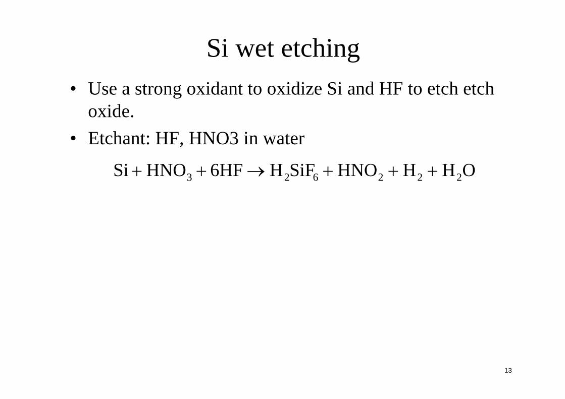
Si wet etching•Use a strong oxidant to oxidize Si and HF to etch etch
oxide.•Etchant: HF, HNO3 in water
OHHHNOSiFH6HFHNOSi 222623

14
Etch rate of Si in HF and HNO3•Acetic acid (CH3COOH or HC2H3O2) is used
as a diluent rather than water.

15
Etchants for GaAs•H2SO4-H2O2-H2O system

16
Directional wet etchants•For Si: mixtures of
KOH, isopropyl alcohol,water. 23.4:13.5:63mixture etches 100times faster in (100)than in (111). Thisetchant contains no HF,a thermal oxide can beused as masking layer.

17

18
Wet etching•Br2-CH3OH for GaAs directional wet etch•Doing selective etch: 1:3:8 mixture of
HF/HNO3/CH3COOH. Etch rate of either typeof heavily doped (>1019 cm-3) layer s of Si is15 times larger than etch rate of lightly dopedlayers.
•Ethylene-diamine-pyrocatechol-water (EDP-water) etches lightly doped Si, but does notattack heavily doped p-type layers.

19
Chemical Mechanical Polishing (CMP)•Achieve global planarization

20
CMP•Earliest process: a thick dielectric, commonly a spin-
on or CVD glass, is first applied.•Wafer is mechanically abraded in alkaline slurry
containing colloidal silica (a suspension of abrasiveSiO2 particles) and an etching agent such as diluteHF.
•KOH and NH4OH are common matrix solutions forthe suspension.
•pH, around 10, is maintained to keep silica particlesnegatively charged to avoid formation of a gel.
•pH buffering agent can be used to ensure stability ofthe process.

21
CMP•Gross mechanical damage is prevented by the
fact that SiP2 particles being used in the slurryare not harder than the film that is beingpolished
•Typical removal rates of SiO2 are severalthousand angstroms per min
•Increase pad pressure increases removal rate,at cost of step height, residual oxide damage,metal contamination

22
CMP•Metal planarization: copper, tungsten•Acidic (pH<3) slurries are used. Theses
slurries do not dorm colloidal suspensions andso agitation must be used to maintainuniformity
•Alumina is the commonly used abrasive fortungsten CMP because it is closer in hardnessto tungsten than most other abrasives.
•Cu is polished in aqueous solution containingparticles several hundred nanometers indiameter. Typical slurries include ammoniumhydroxide, nitric acid, hydrogen peroxide.

23
CMP•Trade off polish goals (uniformity, planarity,
throughput) against cleaning goals (particles scratches,residual ionic and metallic contaminants)
•Postpolish cleaning: megasonic agitation can be usedin combination with a soft pad scrubber or a cleaningsolution to assist in removal of colloidal suspensionfrom wafer.
•Wafer transferred to second pad reserved for cleaning.Transfer be timed to prevent drying of suspension onwafer surface.
•Scratches left behind after CMP may collect metal.Metal filled scratches are called rails. Dilute (100:1)HF may be included to lift off metal particles.

24
Basic regimes of plasma etching•Advantages of plasma etching
–Easier to start and stop–Less sensitive to changes of wafer temperature–High anisotroy–Fewer particles than liquid media–Less chemical waste than wet etching

25
Plasma etch process•A feed gas be broken down into chemically
reactive species by plasma.•These species diffuse to wafer surface. They
move about until react with the exposed film.•Reaction products be desorbed, diffused away
from wafer, transported by gas stream out ofetch chamber

26
Plasma etching•Film surface is subjected to incident flux of
ions, radicals, electrons, neutrals.•Neutral flux is the largest, physical damage is
related to ion flux.•Chemical attack depends on ion flux and
radical flux

27
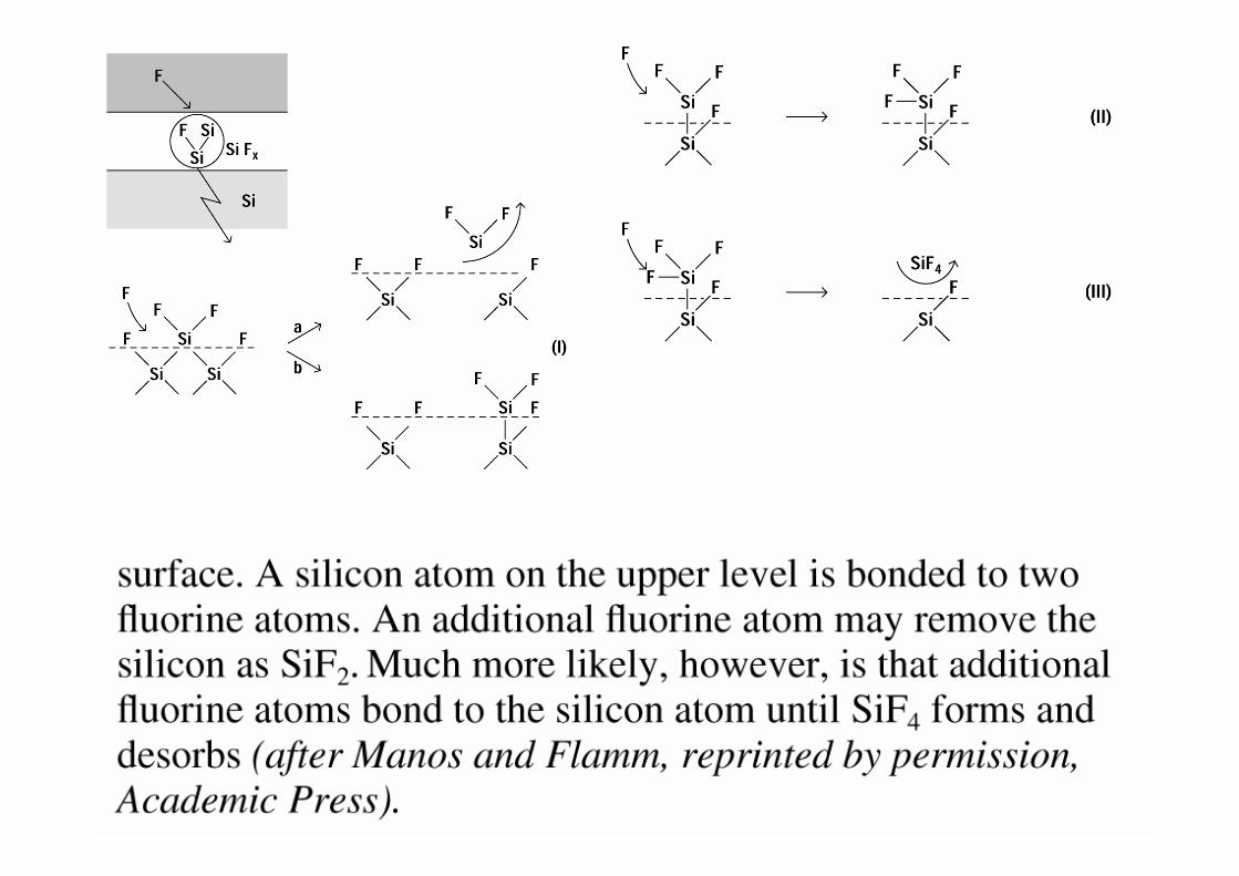
High pressure plasma etching•In CF4 plasma, small ion concentration, etch is
not directly due to ions in plasma. Rather ionbombardment on surface creates unsatisfiedbond that are exposed to reactive radicals.Form volatile products and are pumped away.
•At wafer surface, Si atom is bonded to 2 Fatoms. Both SiF2 and SiF4 are volatile species,but SiF2 will not readily desorb since it ischemically bonded to wafer.
28

29
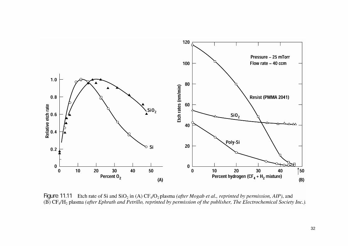
Plasma etching•Possible to use F2 as feed gas, but high
toxicity•Preferred species are CF4, C2F6, SF6, produce
large concentrations of free F.•Addition of small concentrations of O2 to a
CF4 feed gas increase etch rate of Si and SiO2.O2 reacts with C to produce CO2. thisremoves C from plasma, increase Fconcentration.

30

31
•Anisotropic etch:fluorocarbons depositon all surfaces.
•Ion velocity, whichfollows electric field, isvertical. Little ionbombardment onsidewall, fluorocarbonaccumulates
•Process of producingnon-volatile speciesthat reduce etch rate ispolymerization
The film is said to passivate sidewall, prevent lateral etching
32

33
Ion milling•Pure ion milling/ion beam etching: no
chemical reactions, since it uses noble gasessuch as argon.
•A strictly mechanical process•Advantages:
–Directionality: ions are accelerated by a strongelectric field, chamber pressure is low that atomiccollision is not likely. Anisotropic etching ispossible for any material since it is chemistryindependent
–Applicability: it can be used to pattern a widevariety of materials including compounds andalloys

34
Kaufman source•Most popular source of
ion milling•Electron filament
heated using supply VF.Filament is held at avoltage Va belowanode potential.
•Electron boil off offilament and areaccelerated towardanode.
•Electrons impactneutral the neutral gasatoms to ionize them.
•To maintain plasma,source is held at 0.001torr.

35
Kaufman source•A grid held at Vg
accelerates ejectedions toward target
•Ejected ions entertarget chamber
•To maintaindirectional etch,target chamber ispumped to lowpressure, minimizecollisions betweenions and residualgas molecules

36
Ion beam milling•Ions are positively charged, a voltage will
build up on the surface unless wafer and filmbeing etched are conductive
•To avoid charging effect, electron flood gun isused

37
Problems of ion beam milling•Process erode mask layer, any taper
in masking layer be transferred topattern
•Eroded material from target is notvolatile. Some will redeposit onwafer surface, lead to uneven etchand organic residue from resist mask.
•Trenching: mask erosion causessidewalls of the pattern to be taperedat a steep angle. Some of low angleions will reflect off of taperedsurface toward the pattern edge

38
Ion beam milling•An inert species such as argon can be mixed
with small amounts of oxygen to reduceerosion rate of many metals in an ion mill.
•Introducing reactive species tend to attacksource components. In particular, hot filamentis attacked.

39
Reactive ion etching•Need for anisotropic etch with higher
selectivity than ion milling

40
Two common systems for RIE•Chlorine plasma for
anisotropically Si,GaAs, Al etch

41
Chlorine RIE•Undoped Si etch
slowly in Cl/Cl2ambient withoutaddition of ionbombardment
•Heavily n-type dopedSi etches withoutbombardment in Cl,but not in Cl2.
•Doping implies thatCl etching involveselectron transfer fromsubstrate

42
Chlorine RIE model•Atomic Cl chemisorbs
on Si. Once surfaceCl becomesnegatively charged, itcan bond ionicallywith the substrate.This frees additionalchemisorption sitesand increasesprobability that Clatoms penetratesurface and producevolatile siliconchlorides.

43
Cl RIE•Cl penetration is increased by ion
bombardment•Charge transfer produces isotropic etch in
heavily doped layers such as polySi gates andAl metallizations. In these structures, obtainanisotropic etch by sidewall polymerization.
•Sidewall polymerization is done by adjustingrelative concentrations of Cl2 and BCl3, CCl4or SiCl4.

44
Damage in RIE•Residual damage after RIE:
–physical damage–chemical damage

45
Physical Damage in RIE•Etch of SiO2 down to
Si: surface is damagedwith an extensiveconcentration of Si-O,Si-C bonds. H2penetration candeactivate dopants insubstrate.

46
Chemical Damage in RIE•a concern in polymerization etches,
leave behind residual films•Gas particle deposition•Metallic impurities due to sputtering of
electrodes, chamber, fixture in contactwith plasms
47
High-Density Plasma (HDP) etching•High-density sources use crossed magnetic
and electric fields to increase distance the freeelectrons in plasma travel. This, in turn,increase rate of dissociation and ionization.
•High density of ions and radicals can be usedto increase etch rate.
48
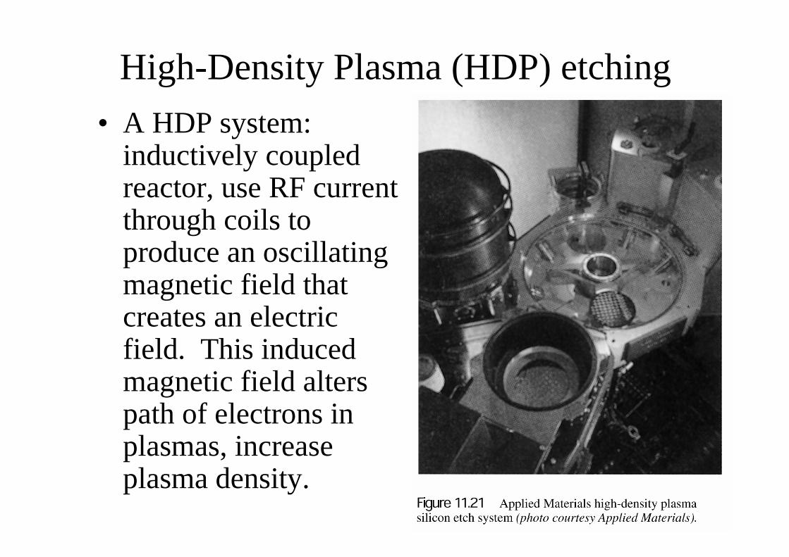
High-Density Plasma (HDP) etching•A HDP system:
inductively coupledreactor, use RF currentthrough coils toproduce an oscillatingmagnetic field thatcreates an electricfield. This inducedmagnetic field alterspath of electrons inplasmas, increaseplasma density.

49
liftoff•An alternative to ion milling for patterning
difficult to etch materials
50
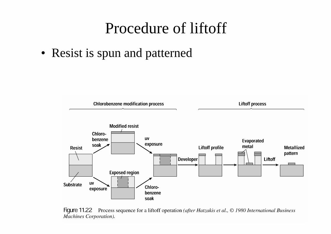
Procedure of liftoff•Resist is spun and patterned

51
Procedure of liftoff•A thin layer of meal is deposited using
evaporation. Evaporation: difficult in coveringhigh aspect ratio features. If a reentrant profileis obtained in resist, a break in metal is assured.

52
Procedure of liftoff•Wafer is immersed n a solution to dissolve
resist.
53
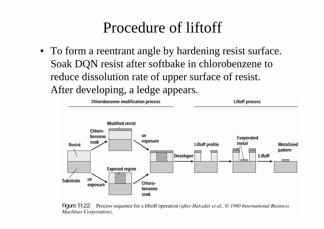
Procedure of liftoff•To form a reentrant angle by hardening resist surface.
Soak DQN resist after softbake in chlorobenzene toreduce dissolution rate of upper surface of resist.After developing, a ledge appears.

54
Shortcoming of liftoff•Surface topology must be smooth, since metal
deposition step has poor step coverage.•Metal lifted off remains solid and floats in bath.
Pieces of it are likely to redeposit on wafersurface.