Embed Size (px)
Citation preview

EC- Objective Paper-I IES-2012 www.gateforum.com
India’s No.1 institute for GATE Training 1 Lakh+ Students trained till date 65+ Centers across India
233
IES-2012- Paper-I
1. The I-V characteristics of a tunnel diode exhibit
(A) current-controlled negative resistance
(B) voltage-controlled negative resistance
(C) temperature-controlled positive resistance
(D) current-controlled positive resistance
2. A gate to drain-connected enhancement mode MOSFET is an example of
(A) an active load (B) a switching device
(C) a three-terminal device (D) a three-terminal device
3. Thermal runway is not possible in FET because, as the temperature of FET increases
(A) the drain current increases (B) the mobility increases
(C) the mobility decreases (D) the transconductance increases
4. The output impedance of a BJT under common-collector configuration is
(A) Low (B) High (C) Medium (D) Very high
5. Consider the following statements related to JFET:
1. Its operation depends on the flow of minority carriers only.
2. It is less noisy than BJT
3. It has poor thermal stability
4. It is relatively immune to radiation
The correct statements are
(A) 1, 2, 3 and 4 (B) 1 and 2 only
(C) 2 and 4 only (D) 3 and 4 only
6. For common-collector amplifier, the current gain (AI) is
(A) fe1 h+ (B) fe
oe L
1 h
1 h R
+
+ (C) fe
oe ie
1 h
h h
+ (D) fe
ie L
1 h
1 h R
+
+
7. Consider the following statements:
(1) Speed of operation of MOSFET is more than the speed of operation of SCR
(2) SCRs have lower power loss than MOSFETs.
(3) The current in conducting state can easily be controlled through the gate in SCR.
(4) MOSFET is not a current triggered device.
The correct statements are
(A) 1 and 4 only (B) 1 and 2 only
(C) 2 and 3 only (D) 1,2,3 and 4

EC- Objective Paper-I IES-2012 www.gateforum.com
India’s No.1 institute for GATE Training 1 Lakh+ Students trained till date 65+ Centers across India
234
8. Match List-I with List-II and select the correct answer using the code given below the
List – I List – II
P. di / dt rating limits 1. Snubber circuit
Q. dv / dt rating 2. Heat sink
R. 2i t limit 3. Series reactor
S. Junction temperature limit 4. Fuse
Codes:
( )
( )
( )
( )
P Q R S
A 2 4 1 3
B 2 1 4 3
C 3 4 1 2
D 3 1 4 2
9. An SCR can be turned off
(A) by passing a negative pulse to its gate
(B) by removing the gate supply
(C) by reverse biasing it
(D) by forcing the current through gate to become zero
10. Body effect in MOSFETs results in
(A) increase in the value of transconductance
(B) change in the value of threshold voltage
(C) decrease in the value of transconductance
(D) increase in the value of output resistance
11. The efficiency of an LED for generating light is directly proportional to the
(A) applied voltage (B) current injected
(C) temperature (D) level of doping
12. A signal f(t) is described as
( )f t 1 t when t 1
0 when t 1
= − ≤
= >
The represents the unit
(A) sinc function (B) area triangular function
(C) signum function (D) parabolic function

EC- Objective Paper-I IES-2012 www.gateforum.com
India’s No.1 institute for GATE Training 1 Lakh+ Students trained till date 65+ Centers across India
235
13. Match List – I with List – II and select the correct answer using the code given below the
Lists:
List – I List – II
(P) Even signal (1) ( ) ( )n
1x n u n
4
=
(Q) Causal signal (2) ( ) ( )x n x n− =
(R) Periodic signal (3) ( ) ( )x t u t
(S) Energy signal (4) ( ) ( )x n x n N= +
Codes:
( )
( )
( )
( )
P Q R S
A 2 3 4 1
B 2 4 3 1
C 1 3 4 2
D 1 4 3 2
14. The period of the signal x(t) = 10sin12 t 4cos18 tπ + π is
(A) 4
π (B)
1
6 (C)
1
9 (D)
1
3
15. A linear time-invariant system has an impulse response of 2te , t > 0. If the initial conditions
are zero and the input is 3te , the output for t > 0 is
(A) e3t – e
2t (B) e
5t (C) e
3t + e
2t (D) e
t
16. A system described by the following differential equation is initially at rest and then excited
by the input x(t) = 3 u(t):
( )2
2
d y dy4 3y x t .
dtdt+ + = The output y(t) is
(A) t 3t1 1.5e 0.5e− −− + (B) t 3t1 0.5e 1.5e− −− +
(C) t 3t1 1.5e 0.5e− −+ − (D) t 3t1 0.5e 0.5e− −+ +
17. The natural response of an LTI system described by the difference equation
y(n) – 1.5y(n-1) + 0.5y(n – 2) = x(n) is
(A) y(n) = 0.5u(n) – 2(0.5)nu(n) (B) y(n) = 0.5u(n) – (0.5)
nu(n)
(C) y(n) = 2u(n) – 0.5(0.5)nu(n) (D) y(n) = 2u(n) – (0.5)
nu(n)
EC- Objective Paper-I IES-2012 www.gateforum.com
India’s No.1 institute for GATE Training 1 Lakh+ Students trained till date 65+ Centers across India
236
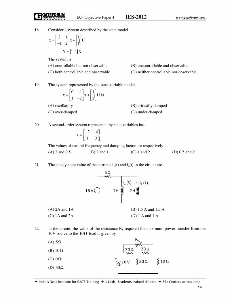
18. Consider a system described by the state model
2 1 1
x x U1 2 1
= + −
[ ]Y 1 1 X=
The system is
(A) controllable but not observable (B) uncontrollable and observable
(C) both controllable and observable (D) neither controllable nor observable
19. The system represented by the state-variable model
0 1 1x x U is
1 2 2
− = + −
(A) oscillatory (B) critically damped
(C) over-damped (D) under-damped
20. A second-order system represented by state variables has
2 4x
1 0
− − =
The values of natural frequency and damping factor are respectively
(A) 2 and 0.5 (B) 2 and 1 (C) 1 and 2 (D) 0.5 and 2
21. The steady-state value of the currents i1(t) and i2(t) in the circuit are
(A) 2A and 1A (B) 1.5 A and 1.5 A
(C) 1A and 2A (D) 1 A and 1 A
22. In the circuit, the value of the resistance RS required for maximum power transfer from the
10V source to the 10Ω load is given by
(A) 5Ω
(B) 10Ω
(C) 0Ω
(D) 30Ω
5Ω
( )1i t ( )2i t
15V +
− 1H 2H
SR
30Ω 30Ω
30Ω 10V 10Ω +
− VS
EC- Objective Paper-I IES-2012 www.gateforum.com
India’s No.1 institute for GATE Training 1 Lakh+ Students trained till date 65+ Centers across India
237
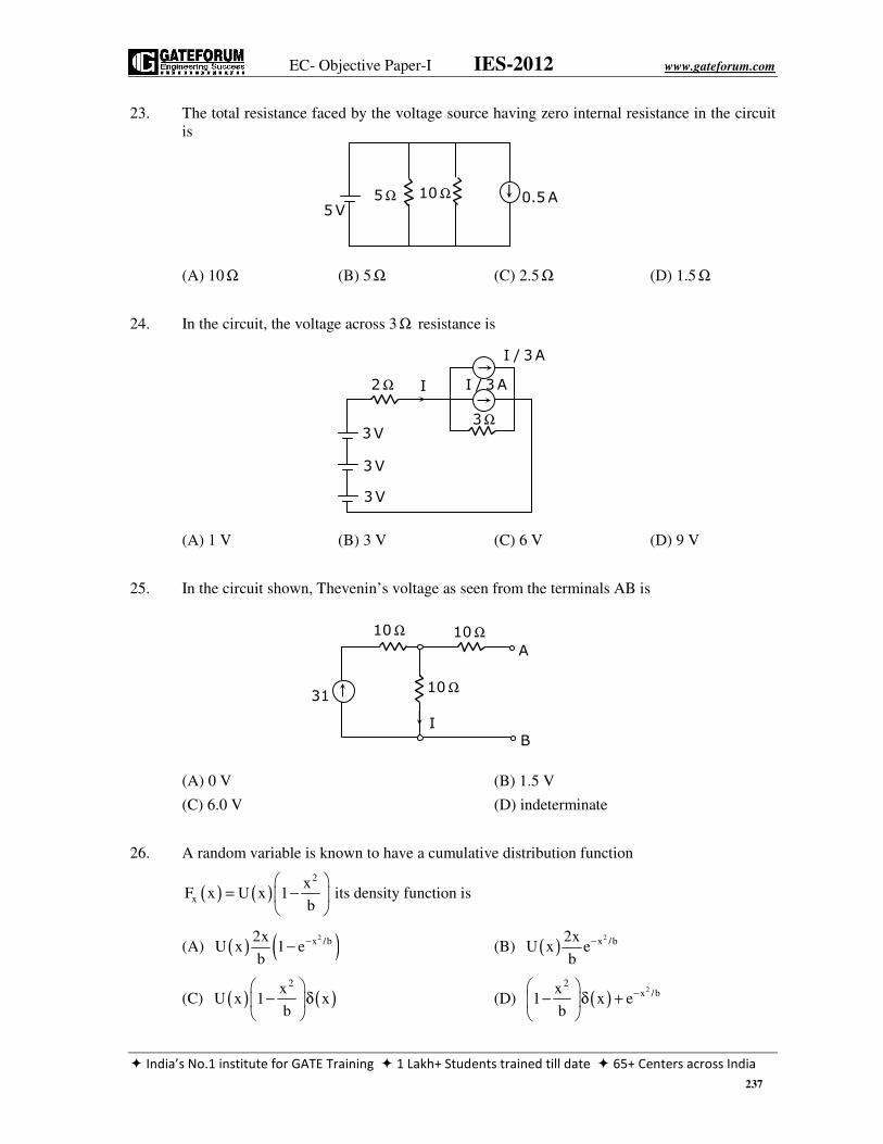
23. The total resistance faced by the voltage source having zero internal resistance in the circuit
is
(A) 10 Ω (B) 5 Ω (C) 2.5 Ω (D) 1.5 Ω
24. In the circuit, the voltage across 3 Ω resistance is
(A) 1 V (B) 3 V (C) 6 V (D) 9 V
25. In the circuit shown, Thevenin’s voltage as seen from the terminals AB is
(A) 0 V (B) 1.5 V
(C) 6.0 V (D) indeterminate
26. A random variable is known to have a cumulative distribution function
( ) ( )2
x
xF x U x 1
b
= −
its density function is
(A) ( ) ( )2x /b2x
U x 1 eb
−− (B) ( )2x /b2x
U x eb
−
(C) ( ) ( )2x
U x 1 xb
− δ
(D) ( )
22
x /bx1 x e
b
− − δ +
5Ω 10Ω 0.5A 5V
2Ω
I / 3A
I / 3A
3Ω
I
3V
3V
3V
10Ω 10Ω
10Ω
A
B I
31

EC- Objective Paper-I IES-2012 www.gateforum.com
India’s No.1 institute for GATE Training 1 Lakh+ Students trained till date 65+ Centers across India
238
27. The probability cumulative distribution function must be monotone and
(A) Increasing (B) decreasing
(C) Non-increasing (D) non-decreasing
28. The step response of a discrete time system with transfer function ( )( )( )
10H Z
Z 1 Z 2=
− + is
given by
(A) ( )n10 10 10
n 29 3 9
−+ + − (B) ( )
nn5 2
2− + + −
(C) ( )n7 5
n 39 3
−+ + − (D) ( )n2 5 1 2− + −
29. The Z-transform corresponding to the Laplace transform function
( )( )
10G s
s s 5=
+ is
(A) ( ) ( )
5z
T
2Ze
Z 1 Z e
−
−− − (B)
( )( ) ( )
5z
5T
2 1 e Z
Z 1 Z e
−
−
−
− −
(C) ( )
5T
2
e
Z 1
−
− (D)
( )
T
3T
e
Z Z e
−
−−
30. The difference equation for a system is given by
( ) ( ) ( ) ( ) ( )y n 2 y n 1 0.16y n x n 1 0.32x n+ + + + = + +
The transfer function of the system is
(A) 2
Z 0.32
Z Z 0.16
+
+ + (B)
2
1
Z Z 0.16+ +
(C) 2
Z 0.32
Z 0.16
+
+ (D)
( )( )2
Z 0.32
Z 1 Z Z 0.16
+
− + +
31. The discrete time system described by 2y(n) x(n)= is
(A) Causal and linear (B) causal and non-linear
(C) Non-causal and linear (D) non-causal and non-linear
32. The impulse response of a discrete time system is given by
( ) [ ] [ ]( )1
h n n n 22
= δ + δ −
The magnitude of the response can be expressed as
(A) cosΩ (B) cosΩ (C) sin Ω (D) sin Ω
EC- Objective Paper-I IES-2012 www.gateforum.com
India’s No.1 institute for GATE Training 1 Lakh+ Students trained till date 65+ Centers across India
239
33. ( )jH e ω is the frequency response of a discrete time LTI system and ( )j1H e ω is the
frequency response of its inverse function. Then
(A) ( ) ( )j j1H e H e 1ω ω = (B) ( ) ( ) ( )j j
1H e H eω ω = δ ω
(C) ( ) ( )j j1H e *H e 1ω ω = (D) ( ) ( ) ( )j j
1H e * H eω ω = δ ω
34. With the following equations, the time-invariant systems are
(1) ( )
( ) ( ) ( )2
2
d y t d2t y t 5y t x t
dtdt+ + =
(2) ( ) ( )2x ty t e
−=
(3) ( ) ( )2
dy t x t
dt
=
(4) ( ) ( )2tdy t e x t
dt
− =
(A) 1 and 2 (B) 1 and 4 (C) 2 and 3 (D) 3 and 4
35. If F(s) and G(s) are the Laplace transforms of f(t) and g(t), then their product F(s). G(s) =
H(s), where H(s) is the Laplace transform of h(t), is defined as
(A) ( )( )f .g t (B) ( ) ( )t
0f g t dgτ − τ τ∫
(C) ( ) ( )Both a and b are correct (D) ( ) ( )f t . g t
36. Consider a system with transfer function
( )2
2
3s 2H s
s 3s 2
−=
+ +
The step response of the system is given by
(A) ( ) ( ) ( )2t tC t 5e e 1 u t− −= − − (B) ( ) ( ) ( ) ( )2t tC t 3 t 10e u t e u t− −= δ − +
(C) ( ) ( ) ( )t 2tC t 4e e 1 u t− −= − − (D) ( ) ( ) ( )2tC t 2 1 e u t−= −
37. The Fourier transform of a rectangular pulse is
(A) another rectangular pulse (B) triangular pulse
(C) sinc function (D) impulse function
38. The function which has its Fourier transform, Laplace transform and Z-transform unity is
(A) Gaussian (B) impulse (C) sinc (D) pulse

EC- Objective Paper-I IES-2012 www.gateforum.com
India’s No.1 institute for GATE Training 1 Lakh+ Students trained till date 65+ Centers across India
240
39. The property of Fourier transforms which states that the compression in time domain is
equivalent to expansion in the frequency domain is
(A) duality (B) scaling
(C) time scaling (D) frequency shifting
40. A waveform is given by ( )v t 10sin 2 100t.= π . What will be the magnitude of the second
harmonic in its Fourier series representation?
(A) 0 V (B) 20 V (C) 100 V (D) 200 V
41. Thevenin’s equivalent resistance as seen from the terminals AB for the circuit is
(A) 1kΩ (B)10Ω (C) 100Ω (D) 10kΩ
42. The total power developed in the circuit, if oV 125V= is
(A) 0 watt (B) 4000 watts
(C) 8000 watts (D) 16000 watts
43. In the circuit given, the switch is closed at t = 0+. The initial voltages on the capacitors are
indicated in the diagram. The voltages Vcl(t) and Vc2(t) for t 0≥ are respectively
1KΩ
A
B
1V 99I
I
+
− SV
t 0= 4MΩ
0.5 Fµ ( )C2V t 0.5 Fµ
+
−
+
−
( )c1V t
( )c1V 0 1V− = ( )c2V 0 1V− =
2V
1V +
−
10A
50A
+
−
+
−
75V
yI 0V x5I
+
− yI
XI
EC- Objective Paper-I IES-2012 www.gateforum.com
India’s No.1 institute for GATE Training 1 Lakh+ Students trained till date 65+ Centers across India
241
(A) ( ) ( )t t1 11 e and 1 e
2 2
− −− + (B) ( ) ( )t t11 e and 1 e
2
− −− +
(C) ( ) ( )t t1 11 e and 1 e
2 2
− −+ + (D) ( ) ( )t t /21 11 e and 1 e
2 2
− −+ +
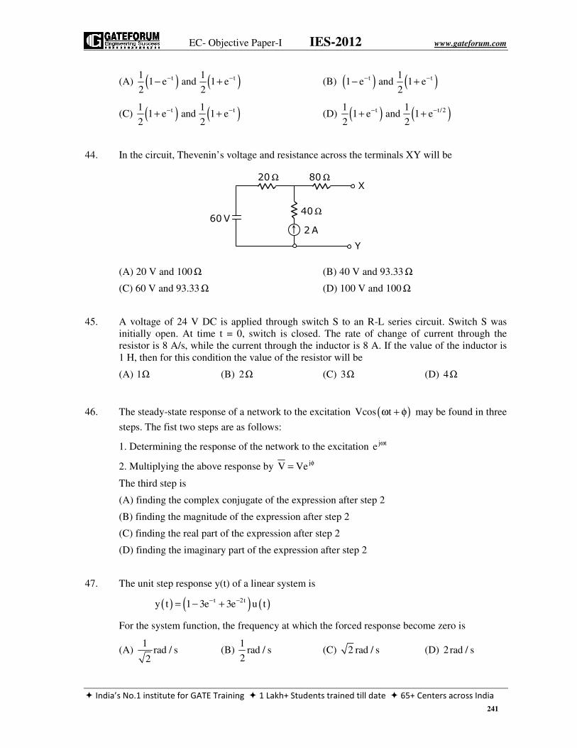
44. In the circuit, Thevenin’s voltage and resistance across the terminals XY will be
(A) 20 V and 100 Ω (B) 40 V and 93.33 Ω
(C) 60 V and 93.33 Ω (D) 100 V and 100 Ω
45. A voltage of 24 V DC is applied through switch S to an R-L series circuit. Switch S was
initially open. At time t = 0, switch is closed. The rate of change of current through the
resistor is 8 A/s, while the current through the inductor is 8 A. If the value of the inductor is
1 H, then for this condition the value of the resistor will be
(A) 1Ω (B) 2Ω (C) 3Ω (D) 4Ω
46. The steady-state response of a network to the excitation ( )Vcos tω + φ may be found in three
steps. The fist two steps are as follows:
1. Determining the response of the network to the excitation j te ω
2. Multiplying the above response by jV Ve φ=
The third step is
(A) finding the complex conjugate of the expression after step 2
(B) finding the magnitude of the expression after step 2
(C) finding the real part of the expression after step 2
(D) finding the imaginary part of the expression after step 2
47. The unit step response y(t) of a linear system is
( ) ( ) ( )t 2ty t 1 3e 3e u t− −= − +
For the system function, the frequency at which the forced response become zero is
(A) 1
rad / s2
(B) 1
rad / s2
(C) 2 rad / s (D) 2 rad / s
20Ω 80Ω X
Y
40Ω
2A 60V

EC- Objective Paper-I IES-2012 www.gateforum.com
India’s No.1 institute for GATE Training 1 Lakh+ Students trained till date 65+ Centers across India
242
48. For a given connected network and for a fixed tree, the fundamental loop matrix is given by
1 0 0 1 0 0
B 0 1 0 0 0 1
0 0 1 1 1 1
= − − −
The fundamental cut-set matrix Q corresponding to the same tree is given by
( )1 0 1 1 0 0
A Q 0 0 1 0 1 0
0 1 1 0 0 1
− − =
( )1 0 1 1 0 0
B Q 0 0 1 0 1 0
0 1 1 0 0 1
− = −
( )1 0 1 1 0 0
C Q 0 0 1 0 1 0
0 1 1 0 0 1
= −
( )0 0 0 1 0 0
D Q 0 1 0 0 0 1
1 0 1 1 1 1
= − − −
49. For a two-port network, V1 and V2 given by
1 1 2
2 1 2
V 60I 20I
V 20I 40I
= +
= +
The Y-parameters of the network are
(A)
311
312
321
322
Y 20 10
Y 10 10
Y 10 10
Y 30 10
−
−
−
−
= ×
= − ×
= − ×
= ×
(B)
311
312
321
322
Y 10 10
Y 20 10
Y 20 10
Y 30 10
−
−
−
−
= − ×
= ×
= ×
= − ×
(C)
311
312
321
322
Y 10 10
Y 20 10
Y 20 10
Y 30 10
−
−
−
−
= ×
= − ×
= − ×
= ×
(D)
311
312
321
322
Y 20 10
Y 10 10
Y 10 10
Y 30 10
−
−
−
−
= − ×
= ×
= ×
= − ×
50. The h11 and h22 of a standard T-network with series impedance 2Ω and 7Ω , and shut
branch impedance of 3Ω are
(A) 5 and 10mho respectivelyΩ (B) 10 and 5mho respectivelyΩ
(C) 5 and 0.1 mho respectivelyΩ (D) 10 and 0.2 mho respectivelyΩ
EC- Objective Paper-I IES-2012 www.gateforum.com
India’s No.1 institute for GATE Training 1 Lakh+ Students trained till date 65+ Centers across India
243
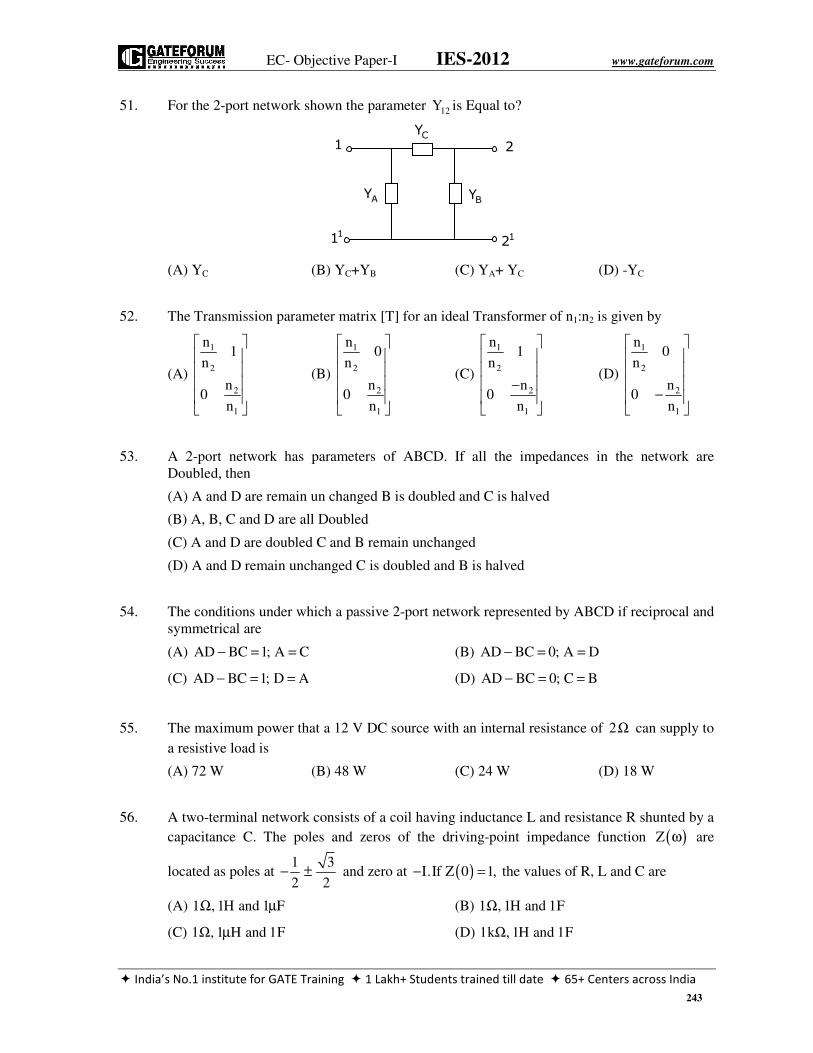
51. For the 2-port network shown the parameter 12Y is Equal to?
(A) YC (B) YC+YB (C) YA+ YC (D) -YC
52. The Transmission parameter matrix [T] for an ideal Transformer of n1:n2 is given by
(A)
1
2
2
1
n1
n
n0
n
(B)
1
2
2
1
n0
n
n0
n
(C)
1
2
2
1
n1
n
n0
n
−
(D)
1
2
2
1
n0
n
n0
n
−
53. A 2-port network has parameters of ABCD. If all the impedances in the network are
Doubled, then
(A) A and D are remain un changed B is doubled and C is halved
(B) A, B, C and D are all Doubled
(C) A and D are doubled C and B remain unchanged
(D) A and D remain unchanged C is doubled and B is halved
54. The conditions under which a passive 2-port network represented by ABCD if reciprocal and
symmetrical are
(A) AD BC 1; A C− = = (B) AD BC 0; A D− = =
(C) AD BC 1; D A− = = (D) AD BC 0; C B− = =
55. The maximum power that a 12 V DC source with an internal resistance of 2Ω can supply to
a resistive load is
(A) 72 W (B) 48 W (C) 24 W (D) 18 W
56. A two-terminal network consists of a coil having inductance L and resistance R shunted by a
capacitance C. The poles and zeros of the driving-point impedance function ( )Z ω are
located as poles at 1 3
2 2− ± and zero at ( )I.If Z 0 1,− = the values of R, L and C are
(A) 1 , 1H and 1 FΩ µ (B) 1 , 1H and 1FΩ
(C) 1 , 1 H and 1FΩ µ (D) 1k , 1H and 1FΩ
CY
AY BY
1 2
11 12

EC- Objective Paper-I IES-2012 www.gateforum.com
India’s No.1 institute for GATE Training 1 Lakh+ Students trained till date 65+ Centers across India
244
57. The condition under which the input impedance at port 1 for the above network will be equal
to R0 is
(A) a b 0Z Z R+ = (B) 2a b 0Z Z R=
(C) a bZ / Z 1= (D) a b
1Z / Z
2=
58. If the potential difference between points A(1, 0, 0) and B(2, 0, 0) is 10 V, determine d for
point C(d, 0, 0), when BCV is 6 V in a uniform field.
(A) 1m (B) 2 m (C) 6 m (D) 5 m
59. There are three charges, which are given by 1 2 3Q 1 C, Q 2 C and Q 3 C.= µ = µ = µ The field
due to each charge at a point P in free space is ( ) ( ) ( )x y z y z x ya 2a a , a 3a and 2a a+ − + −
newtons /coulomb. The total field at the point P due to all three charges is given by
(A) 1.6ax + 2.2ay + 2.5az newtons/coulomb
(B) 0.3ax + 0.2ay + 0.2az newtons/coulomb
(C) 3ax + 2ay + 2az newtons/coulomb
(D) 0.6ax + 0.2ay + 0.5az newtons/coulomb
60. The credit of defining the following current is due to Maxwell
(A) Conduction current (B) Drift current
(C) Displacement current (D) Diffusion current
61. In a digital frequency meter, the Schmitt trigger is used for
(A) Converting sinusoidal waveforms into rectangular pulses
(B) Scaling of sinusoidal waveforms
(C) Providing timebase
(D) Triggering a start pulse
62. The following transducer(s) may employ strain gauge as a secondary transducer
(A) Load cell only
(B) Load cell and torquemeter only
(C) Load cell, torquemeter and accelerometer only
(D) Load cell, torquemeter, accelerometer and flowmeter
aZ
bZ 0R
+
−
0R 0R
+
−
2v 1v

EC- Objective Paper-I IES-2012 www.gateforum.com
India’s No.1 institute for GATE Training 1 Lakh+ Students trained till date 65+ Centers across India
245
63. A Q-meter is supplied with an oscillator having a 500 mV output voltage. While testing an
unknown inductor, the voltage across the variable capacitor of the Q-meter, measured by a
digital voltmeter, is obtained as 10 V. The Q-factor of the inductor is
(A) 5 (B) 10 (C) 20 (D) 0.05
64. Lissajous pattern shown in a double-beam cathode-ray oscilloscope screen for two sinusoidal
voltages of equal magnitude and of the same frequency but of phase shift of o30 electrical is
(A) a circle
(B) a straight line at o45 in the first and third quadrant
(C) an ellipse in the first and third quadrant
(D) an ellipse in the second and fourth quadrant
65. A d’Arsonval meter of 100 DCΩ coil and 0-1 mA sensitivity gives full-scale reading of 10
A on using an external resistance of
(A) 100Ω (B) 10Ω (C) 0.01Ω (D) 0.001Ω
66. The null balance potentiometric measurement of voltage technique in not capable of
measuring
(A) DC voltage
(B) AC voltage
(C) Voltage with higher accuracy and sensitivity as compared to deflection-type instrument
(D) Dynamic and transient voltage changes
67. The following type of instrument can be used for measuring AC voltage of the highest
frequency with reasonable accuracy
(A) Electrodynamometer (B) Moving-iron
(C) Thermal-thermoelectric (D) Rectifier
68. To increase the range of a voltmeter
(A) A low resistance in series is connected with the voltmeter
(B) A low resistance in parallel is connected with the voltmeter
(C) A high resistance in series is connected with the voltmeter
(D) A high resistance in parallel is connected with the voltmeter
69. For the recording of very fast random signals, the most suitable instrument would be
(A) Dual-trace (B) sampling oscilloscope
(c) Real-time spectrum analyzer (D) scanning-type spectrum analyzer
EC- Objective Paper-I IES-2012 www.gateforum.com
India’s No.1 institute for GATE Training 1 Lakh+ Students trained till date 65+ Centers across India
246
70. A resistance is measured by a voltmeter-ammeter method using DC excitation and a
voltmeter of very high resistance connected directly across the unknown resistance. If the
voltmeter and ammeter are subject to maximum error of 2.4%± and 1.0%± respectively,
then the magnitude of maximum error in the value of resistance obtained from the
measurement is nearly
(A) 1.4% (B) 1.7% (C) 2.4% (D) 3.4%
71. During measurement of voltage and current in a load, ammeter and voltmeter are connected
in series and across the load respectively. If ammeter and voltmeter positions are
interchanged by mistake, then
(A) Voltmeter will be damaged (B) ammeter will be damaged
(C) Both the meters will be damaged (D) both the meters will be safe
72. The directivity of a / 2λ long wire antenna is
(A) 1.5 (B) 1.66 (C) 2 (D) 2
73. The ratio of the transverse electric field to the transverse magnetic field is called as
(A) Waveguide impedance (B) waveguide wavelength
(C) Phase velocity (D) Poynting vector
74. Consider a rectangular waveguide of internal dimensions 8 cm x 4 cm. Assuming an H10
mode of propagation, the critical wavelength would be
(A) 8 cm (B) 16 cm (C) 4 cm (D) 32 cm
75.
2 2
2m nn
a b
π π = + − ω µε
represents the propagation constant in a rectangular
waveguide for
(A) TE waves only (B) TM waves only
(C) TEM waves (D) TE and TM waves
76. With the symbols having their standard meaning, cut-off frequency (frequency below which
wave propagation will not occur) for a rectangular waveguide is
(A) 1 m n
a b
π π +
µε (B)
2 21 m n
a b2
π π +
π µε
(C) 1 m n
a b2
π π +
π µε (D)
2 21 m n
a b
π π +
µε
77. A plane wave travelling in a medium of r r1, 1ε = µ = (free space) has an electric field
intensity of100 V / mπ . Determine the total energy density of this magnetic field.
(A) 13.9 3nJ / m (B) 27.8 3nJ / m
(C) 139 3nJ / m (D) 278 3nJ / m

EC- Objective Paper-I IES-2012 www.gateforum.com
India’s No.1 institute for GATE Training 1 Lakh+ Students trained till date 65+ Centers across India
247
78. A / 4λ line, shorted at one end, presents impedance at the other end equal to
(A) Z0 (B) 02Z (C) ∞ (D) 0
Where Z0 is characteristic impedance of the line.
79. A 75 Ω transmission line is first short-terminated and the minima locations are noted. When
the short is replaced by a resistive load RL, the minima locations are not altered and the
VSWR is measured to be 3. The value of RL is
(A) 25 Ω (B) 50 Ω (C) 225 Ω (D) 250 Ω
80. For a plane wave propagating in an unbounded medium (say, free space), the
minimum angle between electric field and magnetic field vectors is
(A) 00 (B) 60
0 (C) 90
0 (D) 180
0
81. Moving-coil permanent magnet instruments can be used for the measurement of
(A) AC and DC (B) AC only
(C) DC only (D) half-wave rectified DC
82. For controlling the vibration of the disc of an AC energy meter, damping torque is produced
by
(A) Eddy current (B) chemical effect
(C) Electrostatic effect (D) magnetic effect
83. Analog inputs are converted to digital outputs using op-amps as comparators.
Assuming a 5-bit digital output, the number of comparators required would be
(A) 32 (B) 31 (C) 64 (D) 63
84. The value of n for the n-bit A/D converter required to convert an analog input in the range of
0 to 5 volts to an accuracy of 10 mV is
(A) 8 (B) 9 (C) 7 (D) 6
85. One of the following can act as an inverse transducer
(A) Electrical resistance potentiometer (B) LVDT
(C) Piezoelectric crystal (D) Capacitive transducer
86. Two strain gauges are used to measure strain in a cantilever, one gauge is mounted on the
top of the cantilever and the other is placed at the bottom. The two strain gauges form two
arms of Whetstone’s bridge. This bridge configuration is called
EC- Objective Paper-I IES-2012 www.gateforum.com
India’s No.1 institute for GATE Training 1 Lakh+ Students trained till date 65+ Centers across India
248
(A) a quarter bridge (B) a half bridge
(C) a full bridge (D) a null bridge
87. A Hall effect transducer is generally used for the measurement of
(A) Power (B) current
(C) Displacement (D) voltage
88. A digital linear displacement transducer normally uses
(A) Straight binary code (B) binary coded decimal
(C) Gray code (D) hexadecimal code
89. The following transducer is used for accurate and precise measurement of temperature
(A) Thermistor
(b) Thermocouple (Alumel / Chromel)
(C) Semiconductor temperature sensor chip
(D) Platinum resistance thermometer
90. Electrical voltage-based telemetering schemes used for short distances must
necessarily have
(A) Low current level only
(B) small signal power only
(C) High signal to noise ratio S
2N
>>
only
(D) All of the above
91. Electrical positional system telemetering uses for transmission of signal in
(A) Two wires only
(B) Two or three wires only
(C) Two or three or four wires only
(D) Two or three or four or even five wires
EC- Objective Paper-I IES-2012 www.gateforum.com
India’s No.1 institute for GATE Training 1 Lakh+ Students trained till date 65+ Centers across India
249
Direction:
Each of the following nine (9) items consists of two statements, one labelled as ‘Statement
(I)’ and the other as ‘Statement (II)’. You are to examine these two statements carefully and
select the answers to these items using code given below:
Code:
(A) Both Statement (I) and Statement (II) are individually true and Statement (II) is the
correct explanation of Statement (I)
(B) Both Statement (I) and Statement (II) are individually true but Statement (II) is not the
correct explanation of Statement (I)
(C) Statement (I) is true but Statement (II) is false
(D) Statement (I) is false but Statement (II) is true
92. Statement (I):
All substances except ferro-magnetic materials which can form permanent magnets, exhibit
magnetic effects.
Statement (II):
Their magnetic effect is due to alignment of dipoles when subjected to an external
electromagnetic field.
93. Statement (I):
Concentration of acceptor atoms in the region between isolation islands in a monolithic
integrated circuit will be much higher than in the p-type substrate.
Statement (II):
The higher density is provided to prevent the depletion region of the reverse-biased isolation
to substrate junction from extending into the p+ type material.
94. Statement (I):
The gate of MOSFET is insulated from the body of FET by deposition of a very thin fragile
layer of SiO2 over the substrate.
Statement (II):
The device is therefore called as an insulated gate field-effect transistor (IGFET).
95. Statement (I):
Z-transform approach is used to analyze the discrete time systems and is also called as pulse
transfer function approach.
Statement (II):
The sampled signal is assumed to be a train of impulses whose strengths, or areas, are equal
to the continuous time signal at the sampling instants.

EC- Objective Paper-I IES-2012 www.gateforum.com
India’s No.1 institute for GATE Training 1 Lakh+ Students trained till date 65+ Centers across India
250
96. Statement (I):
Lossless network functions have only imaginary zeros and poles with only negative real
parts.
Statement (II):
Lossless network functions obey the separation property.
97. Statement (I):
Resistance hygrometer is a good humidity transducer.
Statement (II):
Resistance hygrometer has a sensing element and absorbs or gives up moisture till
equilibrium is reached with ambient water vapour pressure.
98. Statement (I):
Dual-slope A/D converter is the most preferred A/D conversion approach in digital
multimeters.
Statement (II):
Dual-slope A/D converter provides high accuracy in A/D conversion, while at the same time
suppressing the hum effect on the input signal.
99. Statement (I):
RF voltage is measured by rectifying the alternating voltage first and then amplifying the
resulting DC output.
Statement (II):
Amplification of RF signals is itself a very difficult task.
100. Statement (I):
Digital universal counter timer is used to measure time period and frequency of various
circuits which are assembled together to form one complete block.
Statement (II):
Digital counters use logic gates which are selected and controlled by a single front panel
switch known as function switch which can be in either frequency or time-base mode.
101. Diodes are used to compensate which of the following transistor circuit parameters?
1. ICO
2. VBE
3. β
(A) 1 and 2 only (B) 2 and 3 only (C) 1 and 3 only (D) 1, 2 and 3

EC- Objective Paper-I IES-2012 www.gateforum.com
India’s No.1 institute for GATE Training 1 Lakh+ Students trained till date 65+ Centers across India
251
102. The relative values of the forward conduction voltage for a p-n junction diode, a Red LED
and a Schottky barrier diode are
(A) Schottky voltage drop > p-n junction diode drop > Red LED drop
(B) Red LED drop > p-n junction diode drop > Schottky voltage drop
(C) p-n junction diode drop > Schottky voltage drop > Red LED drop
(D) Schottky voltage drop > Red LED drop > p-n junction diode drop
103. A freewheeling diode in a phase-controlled rectifier
(A) improves the line power factor
(B) is responsible for additional reactive power
(C) Prevents inverse operation
(D) is responsible for additional harmonics
104. The following equation describes a linear time-varying discrete time system
(A) y(k + 2) + ky(k + 1) + y(k) = u(k)
(B) y(k + 2) + ky2(k + 1) + y(k) = u(k)
(C) y(k + 2) + 3y(k + 1) + 2y(k) = u(k)
(D) y(k + 2) + y2(k + 1) +ky(k) = u(k)
105. Hall effect is useful for the measurement of a semiconductor’s
(A) Mobility, carrier concentration and temperature
(B) Type (n-type or p-type), conductivity and temperature
(C) Type (n-type or p-type), mobility and carrier concentration
(D) Mobility, conductivity and temperature
106. Given:
N (E) : Density of states
F (E): Probability that a quantum state with energy E is occupied by an electron
EC : Energy level of conduction band
The expression ( ) ( )CE
N E f E dE∞
∫ gives
(A) Minimum number of electrons in conduction band
(B) Concentration of electrons in conduction band
(C) Energy of electron concentration in conduction band
(D) Conductivity of electrons in conduction band

EC- Objective Paper-I IES-2012 www.gateforum.com
India’s No.1 institute for GATE Training 1 Lakh+ Students trained till date 65+ Centers across India
252
107. Non-polar electrolytic capacitors
(A) Are used for applications in AC circuits without any DC polarizing voltage
(B) Contain two capacitors connected in series with opposing polarities
(C) Both (a) and (b) are correct
(D) Both (a) and (b) are wrong
108. The effective capacitance across AB of the infinite ladder shown in the above figure is
(A) ( )1 3 C+ (B) ( )1 7 C+ (C) ( )1 5 C+ (D) ( )1 5
C2
+
109. A capacitor of capacitance C is charged by connecting it to a battery of e.m.f. E. The
capacitor is now disconnected and reconnected to the battery with the polarity reversed. The
heat developed in the connecting wires is
(A) 0.5 CE2 (B) CE
2 (C) 2 CE
2 (D) 3 CE
2
110. The space between the plates of a parallel-plate capacitor of capacitance C is filled with three
dielectric slabs of identical size as shown in the figure. If dielectric constants are
1 2 3, andε ε ε the new capacitance is
(A) C
3 (B)
( )1 2 3 C
3
ε + ε + ε
(C) ( )1 2 3 Cε + ε + ε (D) ( )1 2 3
1 2 3
9 ε + ε + ε
ε ε ε
C C C
C C C C
A
B
A
1ε 2ε 3ε
B
EC- Objective Paper-I IES-2012 www.gateforum.com
India’s No.1 institute for GATE Training 1 Lakh+ Students trained till date 65+ Centers across India
253
111. Superconductors are becoming popular for their use in
(A) Generating very strong magnetic field
(B) Manufacture of bubble memories
(C) Generating electrostatic field
(D) Generating regions free from magnetic field
112. An ideal low-pass filter has a cutoff frequency of 100 Hz. If the input to the filter in volts is
( )v t 30 2= sin 1256t, the magnitude of the output of the filter will be
(A) 0 V (B) 20 V (C) 100 V (D) 200 V
113. A bar magnet made of steel has a magnetic moment of 2.5 A-m2 and a mass of 6.6 x 10³kg.
If the density of steel is 7.9 x10³ kg/m
3, the intensity of magnetization is
(A) 8.3 x10⁻⁷
A/m (B) 3x10⁶A/m
(C) 6.3x10⁻⁷
A/m (D) 8.2x10⁶A/m
114. If the drift velocity of holes under a field gradient of 200 V/m is 100 m/s, their mobility is SI
units is
(A) 0.5 (B) 0.05 (C) 50 (D) 500
115. A flux of 1.2 mWb exerts in a magnet having a cross-section of 230 cm . The flux density in
tesla is
(A) 4 (B) 0.4 (C) 2.5 (D) 40
116. In a transconductance, the device output
(A) Voltage depends upon the input voltage (B) Voltage depends upon the input current
(C) Current depends upon the input voltage (D) Current depends upon the input current
117. A potential barrier of 0.50 V exists across a p-n junction. If the depletion region is 5.0x10⁻⁷
m wide, what is the intensity of the electric field in this region?
(A) 1.0x10⁶V/m (B) 2.5x10
-7V/m (C) 2.5x10
-7V/m (D) 2.5x10
8V/m
118. The concentration of hole-electron pairs in pure silicon at T=300 K is 7x10¹⁵
per cubic
meter. Antimony is doped into silicon in a proportion of 1 atom to 107 atoms. Assuming that
half of the impurity atoms contribute electrons in the conduction band, the factor by which
the number of charge carries increases due to doping (the number of silicon atoms per cubic
meter is 5x1028
) is
(A) 14x1015
(B) 0.5x10²¹
(C) 2.5x10²¹
(D) 1.8x10⁵

EC- Objective Paper-I IES-2012 www.gateforum.com
India’s No.1 institute for GATE Training 1 Lakh+ Students trained till date 65+ Centers across India
254
119. A piece of writing paper that is 10 cm wide, 15 cm long and 0.05 mm thick has a dielectric
strength of 8 kV/mm. If it is placed between two copper plates and subjected to an increasing
voltage, it will break down at
(A) 8 kV (B) 4 kV (C) 0.4 kV (D) 0.8 kV
120. Match List-I with List-II and select the correct answer using the code given below the
List - I List – II
P. Electrostriction 1. Converse of Seebeck effect
Q. Ionic conductivity 2. Reverse effect of piezoelectricity
R. Peltier heat 3. Converse effect of magnetostriction
S. Villari effect 4. Conductivity of insulators
Codes:
( )
( )
( )
( )
P Q R S
A 2 4 1 3
B 2 1 4 3
C 3 4 1 2
D 3 1 4 2