Embed Size (px)
Citation preview

EAGLE Schematic Capture & PCB Layout
Sam DeBruin EECS 373 10/30/2014

Goals • Learn basic PCB crea=on theory
• Learn commands for naviga=ng EAGLE
• Create a new part, place it in a schema=c, and route it into a design
• U=lize tools to check your work

Background It will be helpful to know how much you already know
• EECS 215? • PCB SoOware? • Circuit Design Experience? • Working on an exis=ng project? • (read: does you 373 project have custom aspects)?
• Theory: • ESR? • LDO Design? • Decoupling?

Background It will be helpful to know how much you already know
• More Theory: • Capaci=ve loading on a crystal? • Decoupling capacitors? • Symbolic nets? • PCB as a stack of layers?
• Does anybody have EAGLE installed on their machine in front of them right now?

Theory – Lets make a power supply Equivalent Series Resistance (ESR) -‐ A capacitor has non-‐zero resistance between its terminal and the plate itself
=

Theory – Lets make a power supply Equivalent Series Resistance (ESR) -‐ A capacitor has non-‐zero resistance between its terminal and the plate itself
Low ESR Ceramic ($) Low Value
High ESR Aluminum ($$) High Value
Low ESR Tantalum ($$$) High Value

Theory – Lets make a power supply LDO Design – simple supply and easy to get right, but consider ESR
Low ESR requirement means use at least one ceramic cap, close to the IC

Theory – Signals can Interfere
A high speed digital signal in a wire will act as an antenna

Theory – Signals can Interfere
And will induce a similar signal in adjacent wires

Theory – Signals can Interfere
Worse, it goes both ways!

Theory – Signals can Interfere
Worse, it goes both ways!
Neither signal is usable

Theory – Signals can Interfere
If the antenna analogy doesn’t work for you, its also called
Capaci&ve Coupling
An implied capacitor between the lines, and a capacitor resists changes in voltage

Theory – Signals can Interfere
Either way, solve it with a ground plane (copper poured in-‐between and connected to GND):
For you antenna folks, the plane is a faraday cage
For you capacitor folks, the plane is dominated by two separate capacitors
GND Plane

Theory – Decoupling Power supplies are inherently noisy, microprocessors and other ICs cant handle that Microprocessor App Note will describe decoupling requirements, loca=on is key!
Typically at least one 0.1uF ceramic for every power pin

Theory – Capaci=ve Loading Capaci=ve loads are used to temper crystal oscilla=ons speeds – more capacitance means slower oscilla=on Both the crystal and the microcontroller are expec=ng a certain load This is voodoo magic, best prac=ce is to get the crystal part number from the microcontroller datasheet, and use the capacitor values it recommends

Theory – PCB is a stack of layers Alterna=ng metal and non-‐metal. At least two metal layers, or many more Vias (plated holes) allow signals to move between the layers

Questions about the theory?

Circuit Design – 30,000 feet 1. What is the circuit supposed to do? Where will power
come from? What are the form factor requirements? (concept)
2. Which parts are need to be included to realize goals? (part selec=on) 1. Do you have libraries? (part crea=on)
3. How does it all connect? (schema=c capture -‐ readable)
4. Where does it all go? (PCB layout – no shorts)

EAGLE -‐ Naviga=on • Zoom in/out with the scroll wheel
• Pan by pressing & holding the middle mouse buhon
• Mac mul=touch works well (two finger zoom, three finger pan, etc)
• Otherwise I don’t recommend using a trackpad
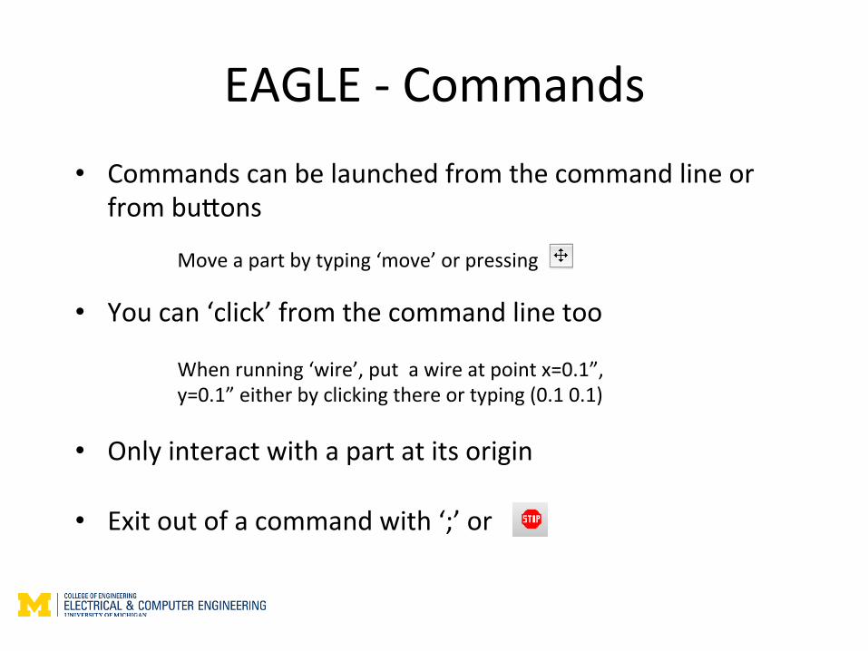
EAGLE -‐ Commands • Commands can be launched from the command line or
from buhons • You can ‘click’ from the command line too
• Only interact with a part at its origin
• Exit out of a command with ‘;’ or
Move a part by typing ‘move’ or pressing
When running ‘wire’, put a wire at point x=0.1”, y=0.1” either by clicking there or typing (0.1 0.1)

EAGLE – Schema=c Capture • Add parts using ‘add’ or
• Copy parts using ‘copy’ or
• Move using ‘move’ or
• Lots of other commands for part manipula=on including ‘rotate’, ‘delete’, ‘mirror’ to be explored

EAGLE – Schema=c Capture • Once you have added parts, connect them with the ‘net’
command ( )
• Net allows you to draw wires between pins, but don’t use ‘wire’!!!
• Difference lies in junc=ons (‘junc’):
vs

EAGLE – Schema=c Capture • Un=l this point, we haven't talked about libraries.
• EAGLE has lots of preloaded parts, but what if you want a different part?
• Make a new library!

EAGLE – Part Crea=on Interlude • Making parts is hard, and you need to be very careful
• Like the pairing of the schema=c capture and the PCB board layout, a Part has mul=ple components
• The Symbol is what goes in the schema=c
• The Package is what goes in the board
• The Part is what links the two. • The part is where you map Symbol pins to
Package pads. Can store pn# too.

EAGLE – Symbol Crea=on • Making the symbol involves placing pins and connec=ng
them with some sort of an outline
• Can include iden=fying symbols and names too • This is the readable version
• Lots of flexibility with how this looks, depends on how you want to see it

EAGLE – Package Crea=on • Making the package involves placing pads and smds
• Can s=ll include a name (called a Reference Designator) • This is the physical version
• Needs to be exactly the size and dimensions of the actual part

EAGLE – Part Crea=on • Part is what you actually add to circuit
• Contains both symbol and package
• Primary func=on is to connect pins from the symbol to pads and smds in the package
• Can also store other info
(ahributes)

EAGLE – Part Crea=on Interlude • The ‘use’ command allows you to add parts from your
new library into the schema=c
• The command ‘use -‐*’ un-‐uses all the default libraries if you want to de-‐cluher and start over
• EAGLE scrip=ng is great for this (outside this scope, but follow up if youre interested).

EAGLE – Schema=c Capture • Other useful commands in the schema=c
• ‘name’ -‐ allows you to assign a net’s name. Nets with the same name will be connected.
• ‘label’ – put a visual label showing a net’s name
• ‘text’ – put text down in the schema=c
• ‘smash’ – move a part’s name label freely
• Don’t forget about supply net symbols! Plus lots more!

EAGLE – Sch -‐> Brd • Once youre (mostly) done type ‘board’ or
And the board is made, although it looks prehy funky

EAGLE – Board Layout • Layout is two interweaving but separate ac=ons: • Placement • Rou=ng
• Don’t be fooled into thinking rou=ng is the important step. A well placed board routes itself (not literally)
• Place based on 1) use and 2) circuit

EAGLE – Rou=ng • Once youre done placing, ‘route’
• Those yellow lines are airwires that represent routes-‐to-‐be
• Quick =ps • ‘route <width>’ will route with a certain width trace • Typing ‘layer <l>’ while rou=ng will place a via and
switch to that layer • Middle click while rou=ng also switches layer • LeO click changes angle style • Run ‘drc’ oOen

EAGLE – Rou=ng • Polygons are large spaces of copper “poured”
(remember a GND pour shields traces) • Polygons on the board are ranked, and will avoid traces
• Generally recommended to pour top and bohom with GND

EAGLE – Checking Your Work • Run ‘erc’: • Checks for inconsistencies between sch and brd • Checks for minor errors in sch (single pin nets)
• Run ‘drc’: (early and oOen!) • Checks for viola=ons of the design rules
• Run ‘rats’: (also early and oOen!) • Re-‐process all polygons • Re-‐draw all airwires to shortest paths • Count remaining airwires (displayed in bohom leO) • ‘rip @;’ hides polygons aOerward
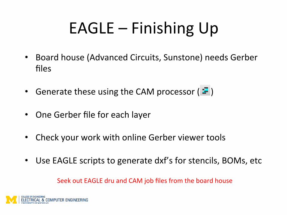
EAGLE – Finishing Up • Board house (Advanced Circuits, Sunstone) needs Gerber
files
• Generate these using the CAM processor ( )
• One Gerber file for each layer
• Check your work with online Gerber viewer tools
• Use EAGLE scripts to generate dxf’s for stencils, BOMs, etc
Seek out EAGLE dru and CAM job files from the board house

PCB Best Prac=ces/Final Checks • Is the silkscreen correct? (Important for assembly) • Is the silkscreen readable? • Are connectors obvious in the silkscreen? • Do parts have part numbers? • Do you have enough test points (1.03mm)? • Can everything be accessed and assembled? • Are LEDs labeled? • Is there a power LED (alive indicator)? • I2c addresses non conflic=ng, CAN stubs short • Name & date & version number in the silkscreen
Questions?
MESH has tutorials complete with sample .sch, .brd, and .lbr files