Embed Size (px)
Citation preview
www.altium.com
EAGLETM MIGRATION GUIDE
TABLE OF CONTENTS
1. THE ALTIUM DESIGNER PHILOSOPHY
2. BE READY TO IMPORT EAGLETM FILES
� Importer Installation
� Supported EagleTM Versions & File Formats
3. TRANSLATING YOUR SCHEMATICS AND PCBS
� Design Data Import Process
4. CLEANING UP YOUR IMPORTED DESIGN
� Schematic Cleanup
� PCB Design Cleanup
� Project Management
� Synchronization
� Engineering Change Orders
5. TRANSLATING YOUR LIBRARIES
� Library Import Process
� Library Cleanup
6. YOUR NEXT STEPS IN ALTIUM DESIGNER
www.altium.com
EAGLETM MIGRATION GUIDE
THE ALTIUM DESIGNER PHILOSOPHYThe core principle of Altium Designer is a unified approach to PCB design. In implementing this approach, you’ll find that our
tool differs from many of the more conventional alternatives currently available. There are a number of separate yet connected
elements required to complete a successful PCB design, and our workflow brings them all together.
As an existing EagleTM user, you’re likely used to having a tool enabling you to do schematic and PCB work in a basic way. But
how do you solve today’s needs when it comes to high-speed design tasks or requirements from mechanical departments?
And what about documentation? A set of gerber files is usually not sufficient: BOMs for procurement and production are
necessary as well as documentation of the whole design for different parties with different needs. Of course those things can
be done with third-party tools. Throughout our tenure in PCB design, the question we’ve always asked is this: Is that approach
really effective?
When we first created Altium Designer, we wanted to create an experience that kept the engineer in complete control of their
efficiency and workflow throughout the entire design process. Achieving this goal meant getting to the heart of the matter:
what, exactly, does a complete PCB design experience entail for the everyday engineer? As part of our approach, we connected
the following processes into a single interface:
� Schematic Capture
� Board Layout
� Design Data Management
� Rules and Constraints
� Bill of Materials
� Supply Chain Integration
� Engineering Change Management
� MCAD Collaboration
� Manufacturing Documentation
With all of these elements integrated into a single, all-encompassing interface, switching back and forth between tasks becomes
as simple as selecting the appropriate file to work on in your design workspace. The interface then handles all the rest and
provides the tools you need for the particular task at hand.
Our unified PCB design approach has continued to grow and evolve over 30 years of research and development. We’ve found
it to be, quite simply, the most efficient way to design electronics. This philosophy extends not just to the individual engineer,
but also to the entire design team.
Multiple engineers can all work on different aspects of the same project using
the same interface, and no time is wasted translating design data back and forth
between design environments.
We hope you enjoy your journey into the world of Altium Designer.
Christian Keller, Technical Sales Manager & The Altium Designer Team.
www.altium.com
EAGLETM MIGRATION GUIDE
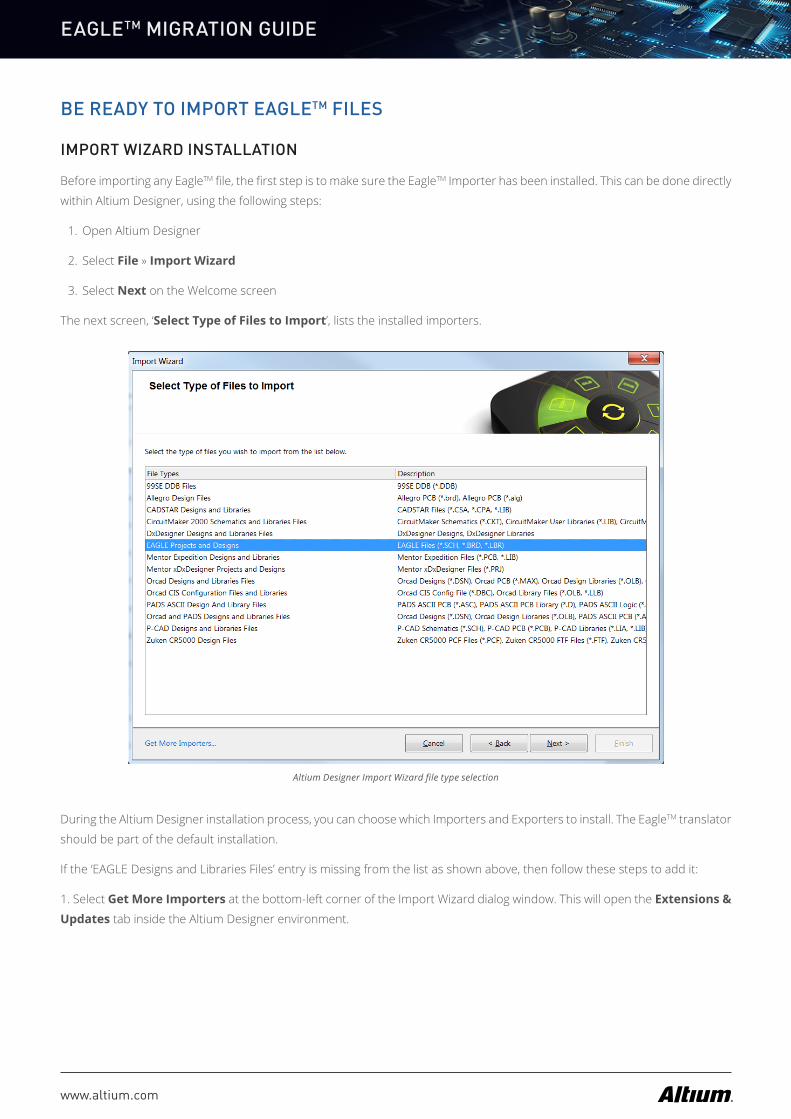
BE READY TO IMPORT EAGLETM FILES
IMPORT WIZARD INSTALLATION
Before importing any EagleTM file, the first step is to make sure the EagleTM Importer has been installed. This can be done directly
within Altium Designer, using the following steps:
1. Open Altium Designer
2. Select File » Import Wizard
3. Select Next on the Welcome screen
The next screen, ‘Select Type of Files to Import’, lists the installed importers.
Altium Designer Import Wizard file type selection
During the Altium Designer installation process, you can choose which Importers and Exporters to install. The EagleTM translator
should be part of the default installation.
If the ‘EAGLE Designs and Libraries Files’ entry is missing from the list as shown above, then follow these steps to add it:
1. Select Get More Importers at the bottom-left corner of the Import Wizard dialog window. This will open the Extensions & Updates tab inside the Altium Designer environment.
www.altium.com
EAGLETM MIGRATION GUIDE
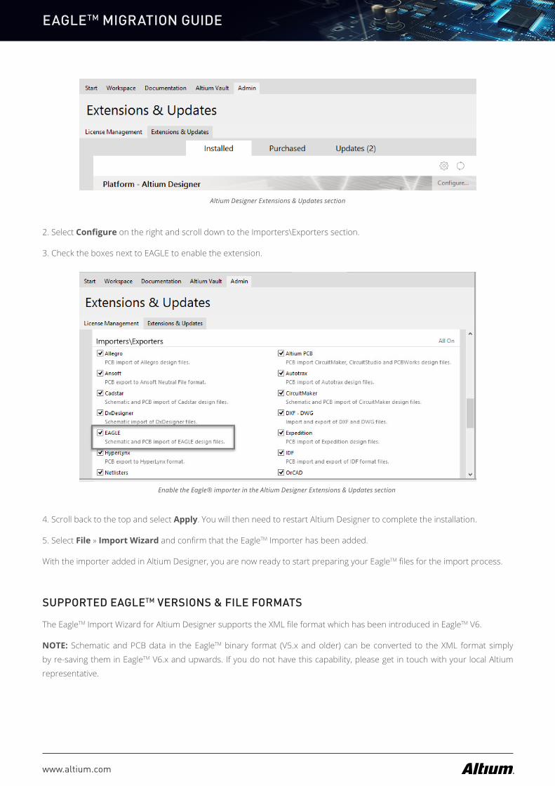
Altium Designer Extensions & Updates section
2. Select Configure on the right and scroll down to the Importers\Exporters section.
3. Check the boxes next to EAGLE to enable the extension.
Enable the Eagle® importer in the Altium Designer Extensions & Updates section
4. Scroll back to the top and select Apply. You will then need to restart Altium Designer to complete the installation.
5. Select File » Import Wizard and confirm that the EagleTM Importer has been added.
With the importer added in Altium Designer, you are now ready to start preparing your EagleTM files for the import process.
SUPPORTED EAGLETM VERSIONS & FILE FORMATS
The EagleTM Import Wizard for Altium Designer supports the XML file format which has been introduced in EagleTM V6.
NOTE: Schematic and PCB data in the EagleTM binary format (V5.x and older) can be converted to the XML format simply
by re-saving them in EagleTM V6.x and upwards. If you do not have this capability, please get in touch with your local Altium
representative.
www.altium.com
EAGLETM MIGRATION GUIDE
TRANSLATING YOUR DESIGN FILES
EAGLETM .SCH SCHEMATIC AND .BRD PCB FILES TO ALTIUM DESIGNER
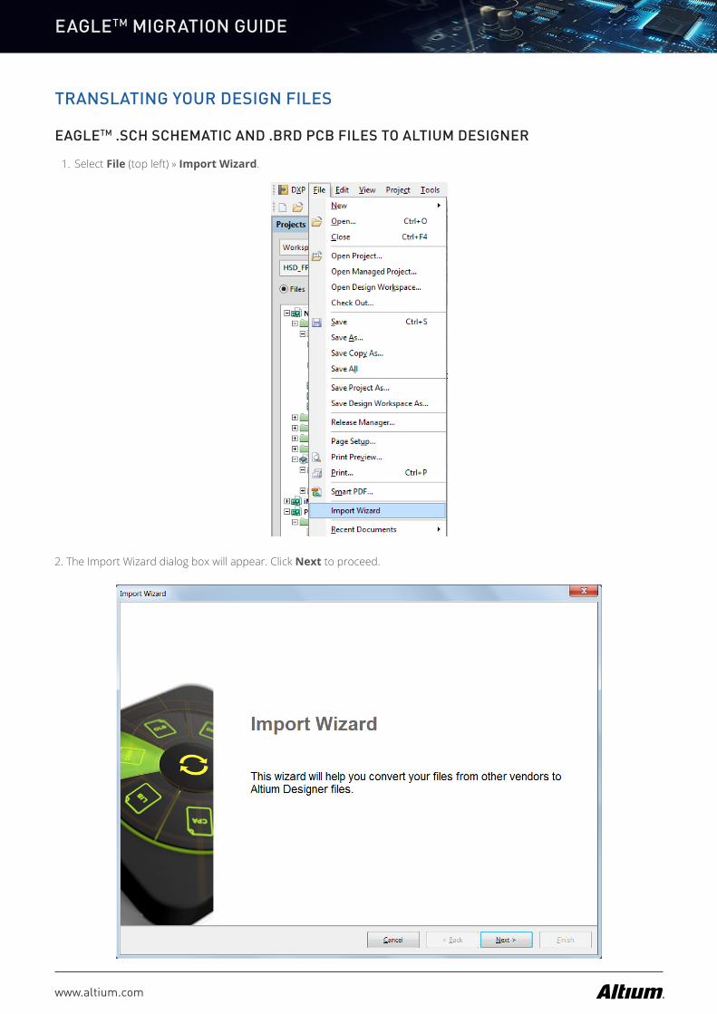
1. Select File (top left) » Import Wizard.
2. The Import Wizard dialog box will appear. Click Next to proceed.
www.altium.com
EAGLETM MIGRATION GUIDE
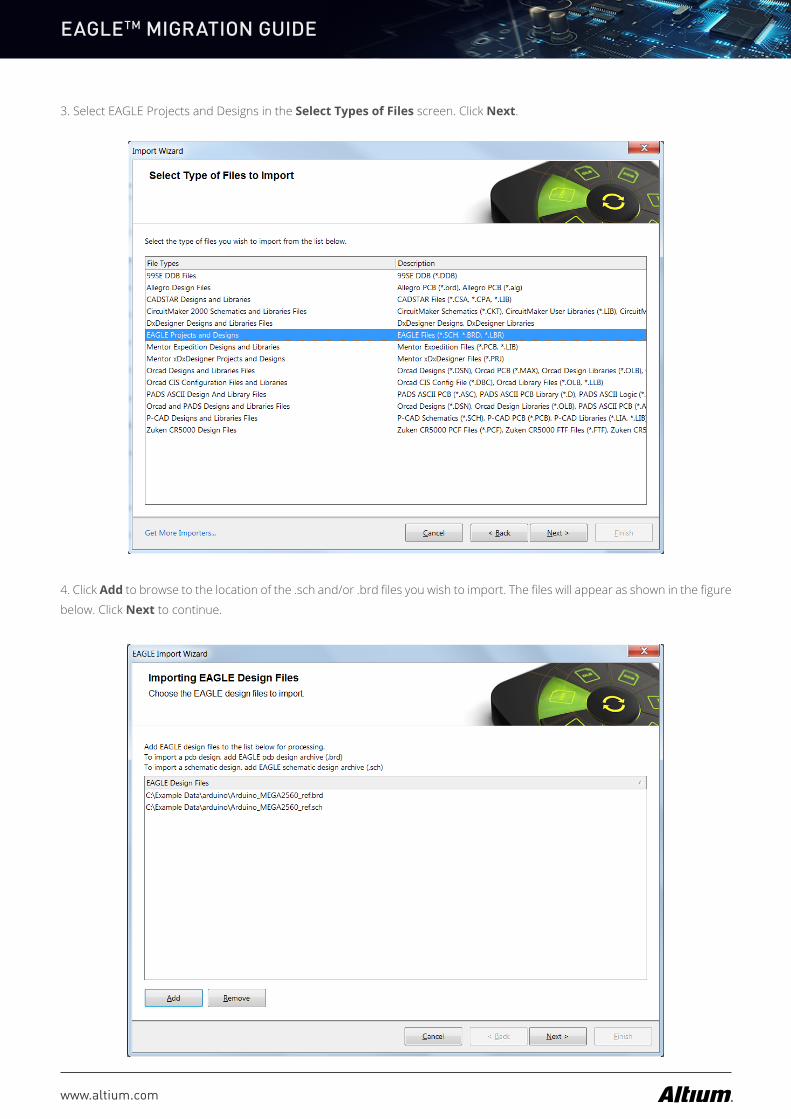
3. Select EAGLE Projects and Designs in the Select Types of Files screen. Click Next.
4. Click Add to browse to the location of the .sch and/or .brd files you wish to import. The files will appear as shown in the figure
below. Click Next to continue.
www.altium.com
EAGLETM MIGRATION GUIDE
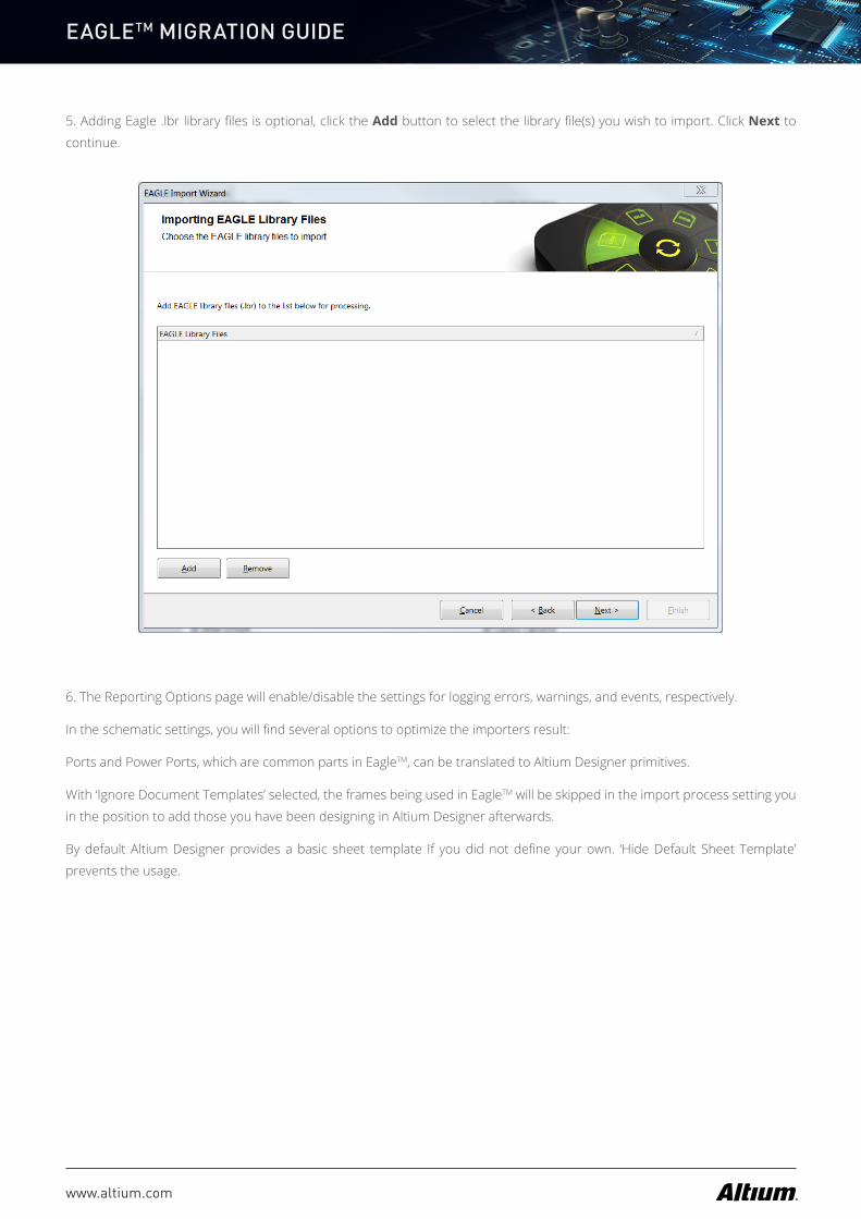
5. Adding Eagle .lbr library files is optional, click the Add button to select the library file(s) you wish to import. Click Next to
continue.
6. The Reporting Options page will enable/disable the settings for logging errors, warnings, and events, respectively.
In the schematic settings, you will find several options to optimize the importers result:
Ports and Power Ports, which are common parts in EagleTM, can be translated to Altium Designer primitives.
With ‘Ignore Document Templates’ selected, the frames being used in EagleTM will be skipped in the import process setting you
in the position to add those you have been designing in Altium Designer afterwards.
By default Altium Designer provides a basic sheet template If you did not define your own. ‘Hide Default Sheet Template’
prevents the usage.

www.altium.com
EAGLETM MIGRATION GUIDE
If you have chosen previously to import libraries as well, the library settings can be adjusted to either be added to the PCB
Project you are importing or imported individually as a Library Project. Click Next to continue.
7. The default project location for the import process is shown below. Click Next to continue.
www.altium.com
EAGLETM MIGRATION GUIDE
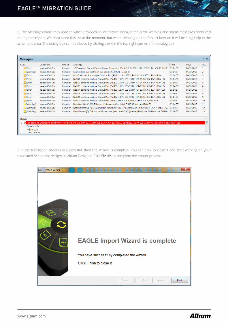
8. The Messages panel may appear, which provides an interactive listing of the error, warning and status messages produced
during the import. We don’t need this list at the moment, but when cleaning up the Project later on it will be a big help in the
schematic area. The dialog box can be closed by clicking the X in the top right corner of the dialog box.
9. If the translation process is successful, then the Wizard is complete. You can click to close it and start working on your
translated Schematic designs in Altium Designer. Click Finish to complete the import process.
www.altium.com
EAGLETM MIGRATION GUIDE
CLEANING UP YOUR IMPORTED DESIGN
PROJECT MANAGEMENT
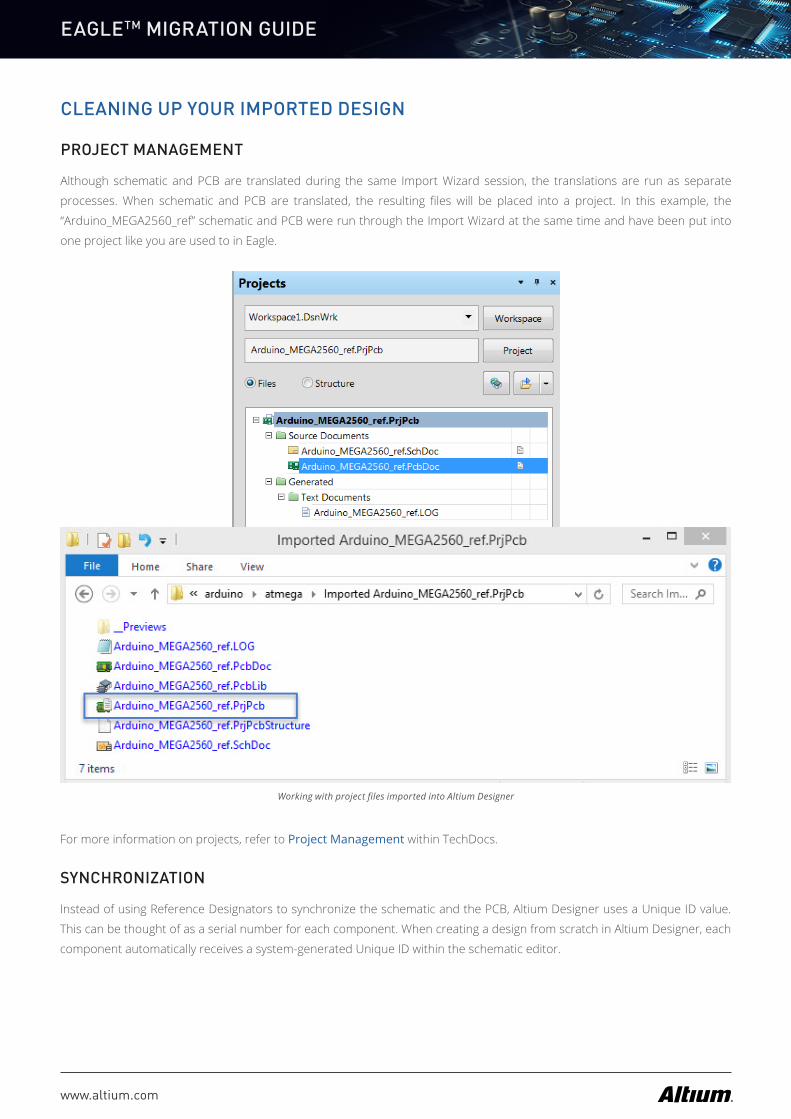
Although schematic and PCB are translated during the same Import Wizard session, the translations are run as separate
processes. When schematic and PCB are translated, the resulting files will be placed into a project. In this example, the
“Arduino_MEGA2560_ref” schematic and PCB were run through the Import Wizard at the same time and have been put into
one project like you are used to in Eagle.
Working with project files imported into Altium Designer
For more information on projects, refer to Project Management within TechDocs.
SYNCHRONIZATION
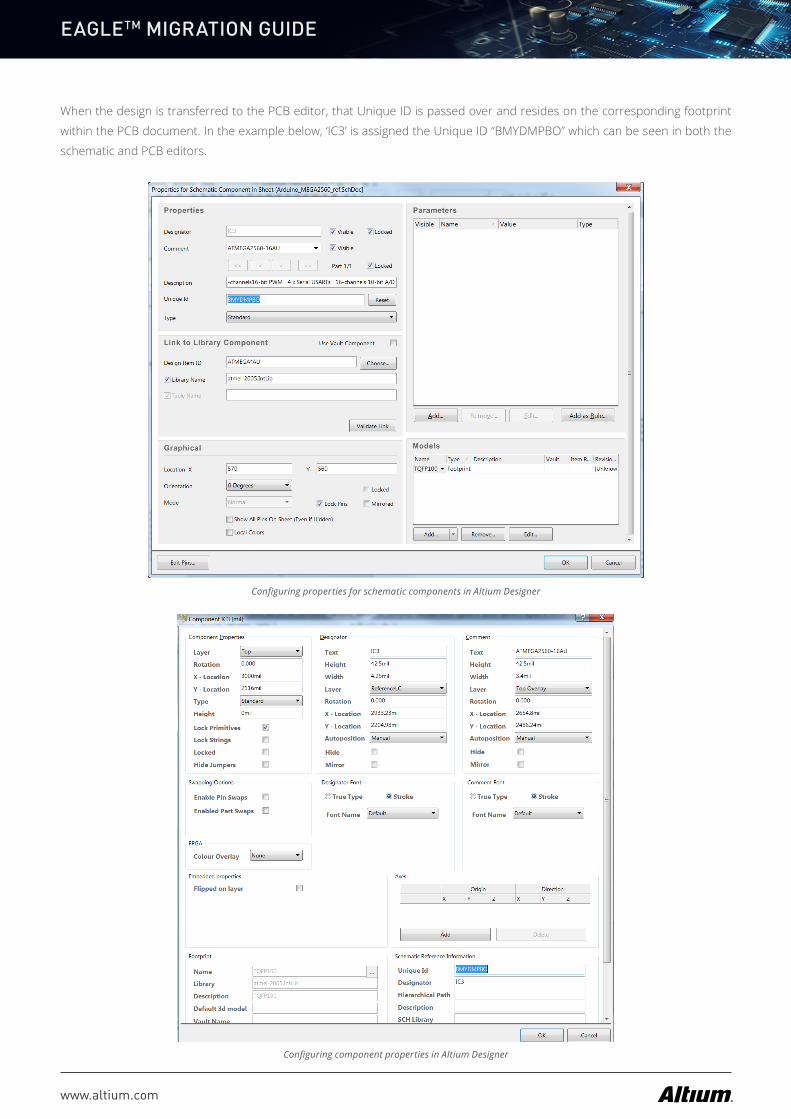
Instead of using Reference Designators to synchronize the schematic and the PCB, Altium Designer uses a Unique ID value.
This can be thought of as a serial number for each component. When creating a design from scratch in Altium Designer, each
component automatically receives a system-generated Unique ID within the schematic editor.
www.altium.com
EAGLETM MIGRATION GUIDE
Configuring properties for schematic components in Altium Designer
Configuring component properties in Altium Designer
When the design is transferred to the PCB editor, that Unique ID is passed over and resides on the corresponding footprint
within the PCB document. In the example below, ‘IC3’ is assigned the Unique ID “BMYDMPBO” which can be seen in both the
schematic and PCB editors.
www.altium.com
EAGLETM MIGRATION GUIDE
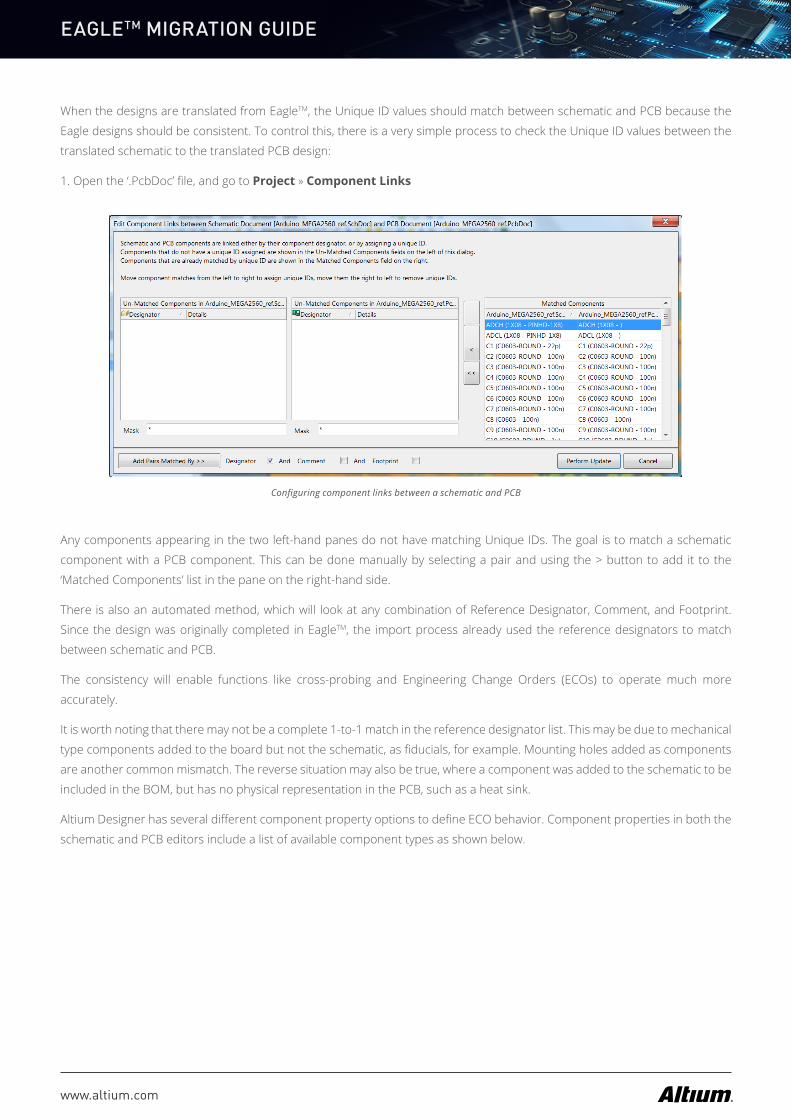
When the designs are translated from EagleTM, the Unique ID values should match between schematic and PCB because the
Eagle designs should be consistent. To control this, there is a very simple process to check the Unique ID values between the
translated schematic to the translated PCB design:
1. Open the ‘.PcbDoc’ file, and go to Project » Component Links
Configuring component links between a schematic and PCB
Any components appearing in the two left-hand panes do not have matching Unique IDs. The goal is to match a schematic
component with a PCB component. This can be done manually by selecting a pair and using the > button to add it to the
‘Matched Components’ list in the pane on the right-hand side.
There is also an automated method, which will look at any combination of Reference Designator, Comment, and Footprint.
Since the design was originally completed in EagleTM, the import process already used the reference designators to match
between schematic and PCB.
The consistency will enable functions like cross-probing and Engineering Change Orders (ECOs) to operate much more
accurately.
It is worth noting that there may not be a complete 1-to-1 match in the reference designator list. This may be due to mechanical
type components added to the board but not the schematic, as fiducials, for example. Mounting holes added as components
are another common mismatch. The reverse situation may also be true, where a component was added to the schematic to be
included in the BOM, but has no physical representation in the PCB, such as a heat sink.
Altium Designer has several different component property options to define ECO behavior. Component properties in both the
schematic and PCB editors include a list of available component types as shown below.
www.altium.com
EAGLETM MIGRATION GUIDE
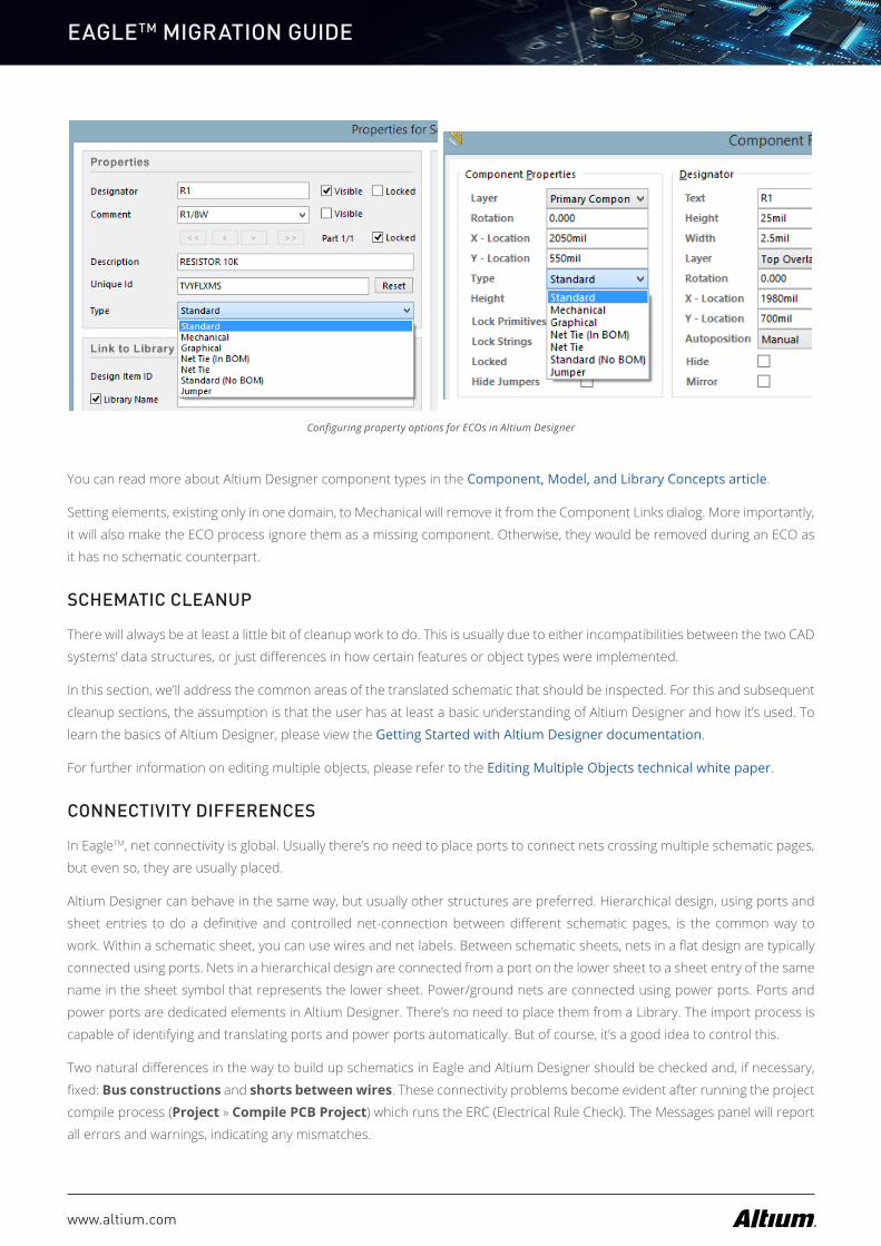
Configuring property options for ECOs in Altium Designer
You can read more about Altium Designer component types in the Component, Model, and Library Concepts article.
Setting elements, existing only in one domain, to Mechanical will remove it from the Component Links dialog. More importantly,
it will also make the ECO process ignore them as a missing component. Otherwise, they would be removed during an ECO as
it has no schematic counterpart.
SCHEMATIC CLEANUP
There will always be at least a little bit of cleanup work to do. This is usually due to either incompatibilities between the two CAD
systems’ data structures, or just differences in how certain features or object types were implemented.
In this section, we’ll address the common areas of the translated schematic that should be inspected. For this and subsequent
cleanup sections, the assumption is that the user has at least a basic understanding of Altium Designer and how it’s used. To
learn the basics of Altium Designer, please view the Getting Started with Altium Designer documentation.
For further information on editing multiple objects, please refer to the Editing Multiple Objects technical white paper.
CONNECTIVITY DIFFERENCES
In EagleTM, net connectivity is global. Usually there’s no need to place ports to connect nets crossing multiple schematic pages,
but even so, they are usually placed.
Altium Designer can behave in the same way, but usually other structures are preferred. Hierarchical design, using ports and
sheet entries to do a definitive and controlled net-connection between different schematic pages, is the common way to
work. Within a schematic sheet, you can use wires and net labels. Between schematic sheets, nets in a flat design are typically
connected using ports. Nets in a hierarchical design are connected from a port on the lower sheet to a sheet entry of the same
name in the sheet symbol that represents the lower sheet. Power/ground nets are connected using power ports. Ports and
power ports are dedicated elements in Altium Designer. There’s no need to place them from a Library. The import process is
capable of identifying and translating ports and power ports automatically. But of course, it’s a good idea to control this.
Two natural differences in the way to build up schematics in Eagle and Altium Designer should be checked and, if necessary,
fixed: Bus constructions and shorts between wires. These connectivity problems become evident after running the project
compile process (Project » Compile PCB Project) which runs the ERC (Electrical Rule Check). The Messages panel will report
all errors and warnings, indicating any mismatches.
www.altium.com
EAGLETM MIGRATION GUIDE
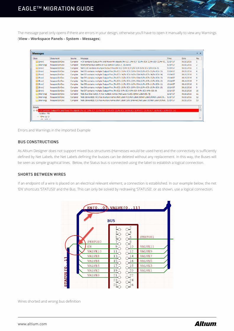
The message panel only opens if there are errors in your design, otherwise you’ll have to open it manually to view any Warnings
(View » Workspace Panels » System » Messages).
Errors and Warnings in the imported Example
BUS CONSTRUCTIONS
As Altium Designer does not support mixed bus structures (Harnesses would be used here) and the connectivity is sufficiently
defined by Net Labels, the Net Labels defining the busses can be deleted without any replacement. In this way, the Buses will
be seen as simple graphical lines. Below, the Status bus is connected using the label to establish a logical connection.
SHORTS BETWEEN WIRES
If an endpoint of a wire is placed on an electrical relevant element, a connection is established. In our example below, the net
‘EN’ shortcuts ‘STATUS0’ and the Bus. This can only be solved by redrawing ‘STATUS0’, or as shown, use a logical connection.
Wires shorted and wrong bus definition
www.altium.com
EAGLETM MIGRATION GUIDE
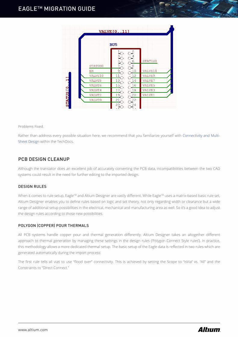
Problems Fixed.
Rather than address every possible situation here, we recommend that you familiarize yourself with Connectivity and Multi-
Sheet Design within the TechDocs.
PCB DESIGN CLEANUP
Although the translator does an excellent job of accurately converting the PCB data, incompatibilities between the two CAD
systems could result in the need for further editing to the imported design.
DESIGN RULES
When it comes to rule setup, EagleTM and Altium Designer are vastly different. While EagleTM uses a matrix-based basic rule set,
Altium Designer enables you to define rules based on logic and set theory, not only regarding width or clearance but a wide
range of additional setup possibilities in the electrical, mechanical and manufacturing area as well. So it’s a good Idea to adjust
the design rules according to those new possibilities.
POLYGON (COPPER) POUR THERMALS
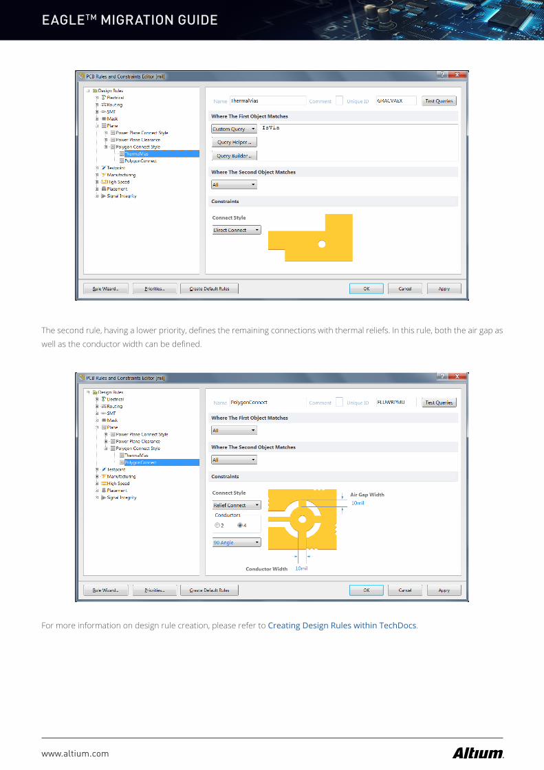
All PCB systems handle copper pour and thermal generation differently. Altium Designer takes an altogether different
approach to thermal generation by managing these settings in the design rules (‘Polygon Connect Style rules’). In practice,
this methodology allows a more dedicated thermal setup. The basic setup of the Eagle data is reflected in two rules which are
generated automatically during the import process:
The first rule tells all vias to use “flood over” connectivity. This is achieved by setting the Scope to “IsVia” vs. “All” and the
Constraints to “Direct Connect.”
www.altium.com
EAGLETM MIGRATION GUIDE
The second rule, having a lower priority, defines the remaining connections with thermal reliefs. In this rule, both the air gap as
well as the conductor width can be defined.
For more information on design rule creation, please refer to Creating Design Rules within TechDocs.
www.altium.com
EAGLETM MIGRATION GUIDE
ENGINEERING CHANGE ORDERS
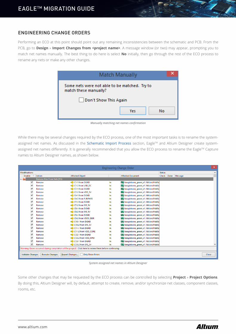
Performing an ECO at this point should point out any remaining inconsistencies between the schematic and PCB. From the
PCB, go to Design » Import Changes from <project name>. A message window (or two) may appear, prompting you to
match net names manually. The best thing to do here is select No initially, then go through the rest of the ECO process to
rename any nets or make any other changes.
Manually matching net names confirmation
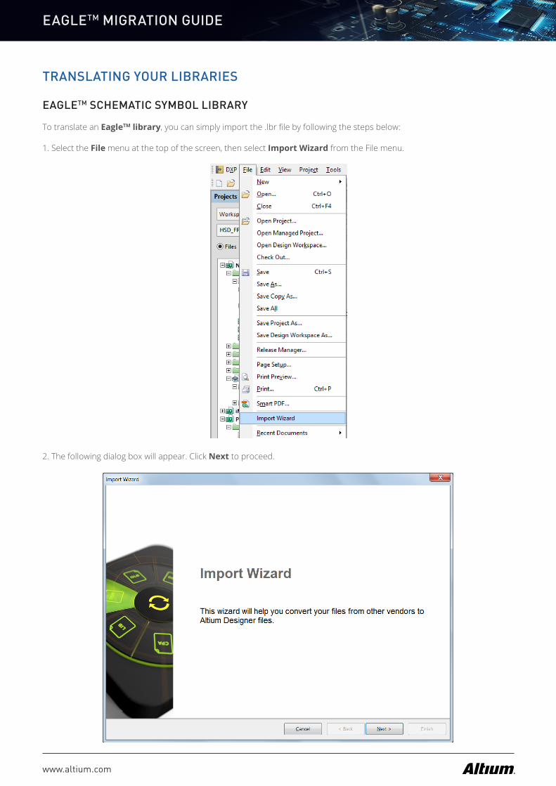
While there may be several changes required by the ECO process, one of the most important tasks is to rename the system-
assigned net names. As discussed in the Schematic Import Process section, EagleTM and Altium Designer create system-
assigned net names differently. It is generally recommended that you allow the ECO process to rename the EagleTM Capture
names to Altium Designer names, as shown below.
System assigned net names in Altium Designer
Some other changes that may be requested by the ECO process can be controlled by selecting Project » Project Options.
By doing this, Altium Designer will, by default, attempt to create, remove, and/or synchronize net classes, component classes,
rooms, etc.

www.altium.com
EAGLETM MIGRATION GUIDE
Configuring project options for an ECO in Altium Designer
It’s up to the user whether to accept these changes or not. The checkboxes in the ECO dialog allow the user to temporarily
disable any particular change. Permanent changes to the types of modifications that are made during an ECO are controlled by
going to the Project » Project Options menu, and then setting up the options in the ECO Generation tab.
There are a number of other situations that can cause the ECO
process to show differences between the schematic and PCB. We
don’t have the time to discuss them all here, but the user should
be able to determine the sources of the differences by using the
concepts we’ve provided. For more information, go to Finding
Differences and Synchronizing Designs within TechDocs.
Your ultimate goal is to receive a message after performing an
update that indicates that no ECO will be generated, or that no
differences are found (depending on how your Project Options
are set).
No differences dialog
www.altium.com
EAGLETM MIGRATION GUIDE
TRANSLATING YOUR LIBRARIES
EAGLETM SCHEMATIC SYMBOL LIBRARY
To translate an EagleTM library, you can simply import the .lbr file by following the steps below:
1. Select the File menu at the top of the screen, then select Import Wizard from the File menu.
2. The following dialog box will appear. Click Next to proceed.
www.altium.com
EAGLETM MIGRATION GUIDE
3. Select the file type you wish to import (Eagle Designs and Libraries Files). Click Next.
4. Click the ‘Next’ button to skip adding Eagle Designs Files. You can translate Design Files at the same time as Library Files (see
above for details).
www.altium.com
EAGLETM MIGRATION GUIDE
5. Click the ‘Add’ button to select the Eagle Library File(s) you wish to import. Click ‘Next’ to continue.
6. Other than the General Settings there is nothing more to adjust in the Reporting Options this time. Click ‘Next’ to continue.
www.altium.com
EAGLETM MIGRATION GUIDE
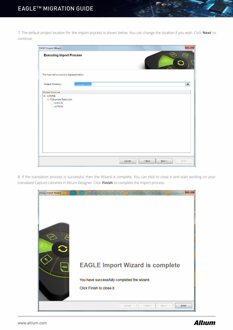
7. The default project location for the import process is shown below. You can change the location if you wish. Click ‘Next’ to
continue.
8. If the translation process is successful, then the Wizard is complete. You can click to close it and start working on your
translated Capture Libraries in Altium Designer. Click ‘Finish’ to complete the import process.
www.altium.com
EAGLETM MIGRATION GUIDE
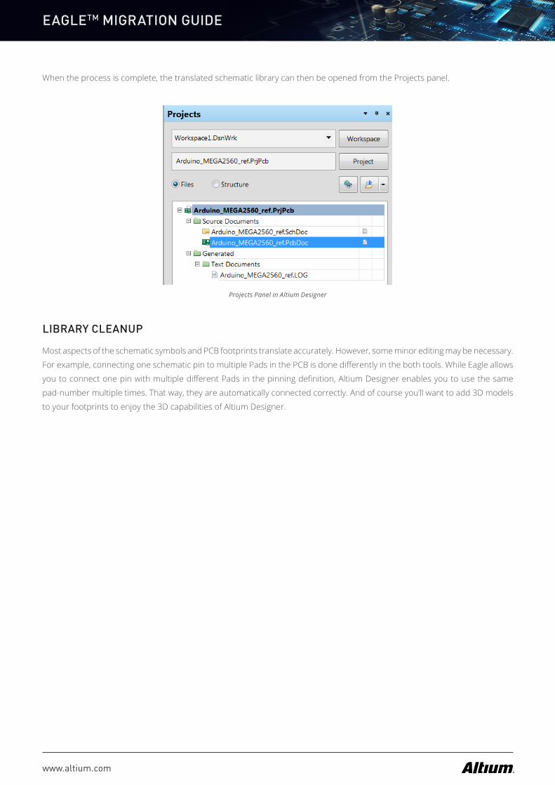
When the process is complete, the translated schematic library can then be opened from the Projects panel.
Projects Panel in Altium Designer
LIBRARY CLEANUP
Most aspects of the schematic symbols and PCB footprints translate accurately. However, some minor editing may be necessary.
For example, connecting one schematic pin to multiple Pads in the PCB is done differently in the both tools. While Eagle allows
you to connect one pin with multiple different Pads in the pinning definition, Altium Designer enables you to use the same
pad-number multiple times. That way, they are automatically connected correctly. And of course you’ll want to add 3D models
to your footprints to enjoy the 3D capabilities of Altium Designer.
www.altium.com
EAGLETM MIGRATION GUIDE
YOUR NEXT STEPS IN ALTIUM DESIGNEROnce all of your design files are successfully translated from EagleTM, it’s now time to dive deeper into the intricacies of the
Unified Design Environment in Altium Designer. Below are several links to our documentation, video tutorials, and additional
training resources, which will help you make the most of your experience in Altium Designer.
SUPPORT DOCUMENTATION
� Getting Started with Altium Designer - Explore a complete set of tutorials for creating your first schematic and board
layout in Altium Designer.
� The Altium Designer Environment - Get a complete overview of the Unified Design Environment in Altium Designer.
� Library and Component Management - Learn how to easily manage your component libraries within your Altium Designer
workspace.
That’s just a small sampling of the vast archive of Altium Designer documentation we have available. Explore more at techdocs.
altium.com.
VIDEO LIBRARY
Our complete suite of videos includes several tutorials, feature overviews, and more to help get you acquainted with the Altium
Designer environment. View all the available videos in the Altiumlive Video Library.
LIVE TRAINING EVENTS
Prefer a more hands-on approach to your learning? Register for one of our live events, including webinars, training courses,
and seminars. View all the events on the Altium Events page.
NEED ADDITIONAL HELP?
Our support team is always here to assist you with any questions you might have. You can contact us directly through the
Contact Us page.
© 2016 Autodesk. All rights reserved worldwide. Eagle and the Eagle logo are registered trademarks of Autodesk. All others are the property
of their respective holders.