Embed Size (px)
Citation preview

E25/CS25: Principles of Computer Architecture, Spring 2005
Dr. Bruce A. Maxwell, Associate ProfessorDepartment of Engineering
Swarthmore College
Course Description
This course covers the physical and logical design of a computer. topics include current micropro-cessors, CPU design, RISC and CISC concepts, pipelining, superscalar processing, cache, paging, segmentation, virtual memory, parallel architectures, bus protocols, and input/output devices. Labs cover analysis of current systems and microprocessor design using CAD tools, including VHDL. Offered in the spring semester every year.
Prerequisites
: CPSC 35, ENGR 15/CPSC 24, or permission of instructor.
© 2005 Bruce A. Maxwell
This material is copyrighted. Individuals are free to use this material for their own educational, non-commercial purposes. Distribution or copying of this material for commercial or for-profit purposes without the prior written consent of the copyright owner is a violation of copyright and subject to fines and penalties.

E25/CS25 Lecture #1 S05
Overall Topic: Vocabulary, Introduction to computer structure
Syllabus
• Course web page: http://www.palantir.swarthmore.edu/maxwell/classes/e25/• Syllabus, homework, and all labs will be on the web page.
• Homework #1 is already there• Office hours, email• Lab assistants/graders (TBA)• Textbooks: Stallings 6th ed., homeworks will be from Stallings.• Exam dates: Feb 18, March 25, April 22 (all 50 minute exams)• Grading: HW 10%, Labs + Project 40%, Exams I, II, and III 30% total, Final 20%• Weekly homework, late homework receives no credit• 5 labs over 14 weeks on a 2-3-week schedule, divide into groups of 2 or 3• First lab meeting is Monday at 1:30/2:45. I will cover how to use the Altera CAD environment
and VHDL which you will be using for assignment #1. At least one person from each lab group must be there.
• If you do the required work on a lab, and do it well, your group will receive a B+. An A of some kind requires extension of the lab. I will always suggest several extensions, but you are free to pursue your own.
• Academic honesty
Introductions
1. What was your first memory of using a computer?2. Have you ever opened up a computer and looked inside?3. Your name, major, class4. Food and color
Where computer architecture fits...
Computer architecture and organization sits at the boundary of com-puter science and engineering. It connects mathematics and physics through the development of an emminently practical device.
• Above is computer system design and operating systems.• Below is digital system and VLSI design.
Computer architecture is largely history• Most of the main concepts in computer architecture were
developed early on• Most current advances in architecture are incremental (with some exceptions)• Hardware has, for the most part, advanced faster than software or architecture concepts• Moore’s Law shows few signs of slowing
• The number of transistors on a chip doubles every 18 months• Cost per bit falls exponentially• Power per bit falls exponentially, speed rises, and reliability increases
Mathematics
Algorithms
Applications
Operating Systems
Architecture
Organization
Digital Logic
VLSI Design
Semiconductor Manf.
Phyics

Tools
Computer architecture is also about tools.• Apple used a Cray to design the mac plus• Cray used an Apple to design the next generation of supercomputer
Computers are large circuits, so we need tools to help us design, describe, and debug them.• Design used to be based on drawings and basic chips
• Cray 1 was built from quad 2-input NAND gate chips, wire-wrapped by hand• Today a single chip may contain over 100 million transistors, with multiple CPUs
How do we build and describe these circuits?• The same way we describe and build software that is millions of lines of code• The same way we describe and design buildings or engines
• Hierarchical design with resusable components• Design language for accurate specification of components and their behavior• Simulation environment for faster debug cycle times
VHDL [VHSIC Hardware Description Language]
VHDL is a language for specifying a digital circuit• Can describe the circuit structurally as a set of hardware components and wires
• Structural representation is the most basic• Textual description of a graphical description of the circuit
• Can describe the circuit as data flowing between memory locations• Data moves between variables, which serve as memory locations• Data processing can occur during the moves (combinational circuits)
• Can describe the circuit as implementing a particular function or behavior• Uses a VHDL mode that looks and acts like a programming language• The behavior of the circuit is described as a program (hardware = software)• Circuits described this way are difficult to synthesize efficiently

E25/CS25 Lecture #2 S05
Overall Topic: State machines, computer history
State Machines (Finite State Automata)
• A method of representing sequential behaviors, which is what computers do• The set of possible states is the set of possible configurations of internal registers• You want the circuit to move between states in an appropriate manner
• In a regular way, usually dependent upon a clock cycle• Next state is usually a function of both the current state and some inputs
• State diagrams help us to define the sequential behavior of circuits• Each state is a node• Edges connect the nodes, indicating direction of motion• Quantities on the edges indicate the inputs that cause the edge to be taken• Quantities on the edges after a slash indicate the outputs when an edge is taken
• The output of a state machine can be a function of just the state, or both the state and the input
VHDL State Machine Design Techniques
The standard structure of a state machine is:
• Declare a state variable/register in the architecture• If reset then put the state machine into the reset state• Else if it is a rising edge
• Execute a case statement based on the current value of the state variable• Within each case, test the input conditions and update the state and output variables
We give the synthesizer the task of assigning binary state labels by using an enumerated type.
library ieeeuse ieee.std_logic_1164.all;
entity statemachine isport(Clk, Rst: in std_logic);
end statemachine;
architecture statemachine of statemachine istype States is {Fetch, Decode, Execute, Write};signal State: States;
beginreg:process(Rst, Clk) begin
if Rst = ‘1’ then -- Asynchronous resetState <= Fetch;
elsif (Clk = ‘1’ and Clk’event) thencase State is when Fetch => State <= Decode;when Decode => State <= Execute;when Execute => State <= Write;when Write => State <= Fetch;end case;
end if;end process;
end statemachine1;
00
01
10
11
A state machine that repeats a four state sequence.

A circuit like this might be the basis for the fetch-execute cycle in a computer [CPU]• Fetch state enables the memory to return the next instruction• Decode state analyzes the current instruction and sets up the ALU arguments• Execute state passes the arguments through the data processing part of the CPU• Write state send the results of the data processing to the appropriate location(s)
You might use this circuit to divide a clock signal into four signals, each with a 25% duty cycle• A cycle is one clock period• The % duty indicates the percentage of that period that the clock remains high
Concept of state machines is old, but how to do data processing came first...
Vocabulary
Computer Architecture v. Computer Organization
Architecture - logical design of a computer, allows you to write programs
• Instruction set (what is the instruction set?)• Representation of data types (integers v. characters v. floating point types)• Input/Output mechanisms (how does the computer communicate with the world?)• Memory addressing techniques• Example: IBM 360 computers
• The first “family” of computers, introduced in 1970• The logical architecture of the family is the same, the organization has changed radically• Software written for a 360 system in 1970 still runs, hence Y2K was a problem
• Another example: the x86 implementations of the Intel IA-32 architecture• Software compiled for a 386 will run on anything above it• The 486, 586, and 686 will run them much faster
• One of the more interesting cases of architectures is the Itanium, which has a completely dif-ferent architecture than the IA-32, but still runs IA-32 code in a compatibility mode.
Organization - physical design of a computer
• How many registers • What is a register?• How many registers does a typical CPU have?
• Pentium: 16• Itanium: 64+• G5: 64+
• Floating point unit? • What is a floating point unit?
• Executes floating point computations in hardware• What were the first desktop CPUs with an integrated floating point unit?
• Motorola 68040• Intel 486
• What speed are the CPU clock cycle, the bus, and the memory?• What are typical CPU speeds?
• G5: 1-2GHz; Athlon/Pentium: 1-3.8GHz

• Memory organization• Does the processor have a memory cache?• What is the speed of communication with the memory?
• G5: 8 instructions per cycle, 8 bytes/instruction, 2GHz clock, need potentially 128GBytes of instructions per second from memory (current tech is 8 GB/s)
Structure & Function
What can a computer do?
• Data Processing• Data Storage• Data Movement• Control

E25/CS25 Lecture #3 S05
Overall Topic: Computer structure, computer history
Structure & Function
Level one: The computer is device that can communicate with the outside world, and store and manipulate data.
• The box, which can connect to networks (communica-tion) and peripherals (I/O)
• Software: operating system and applications• Operating system controls the ability of the applications
to function
Level two: The computer has four component parts,
• CPU (Central Processing Unit)• Main Memory (RAM: Random Access Memory)• I/O (Input/Output)• System Interconnection (buses)• The CPU is the overall master of processes
Level three: The CPU has four components
• Arithmetic Logic Unit (ALU)• Floating Point Unit (FPU)• Registers (Data, Instruction, Stack, Integer, Floating
Point)• Control Unit• Internal CPU connections (wires)• The control unit is what makes the other elements func-
tion together
Level four: The control unit has three internal components
• Sequencing logic• Control unit registers and decoders• Control memory• The sequencing logic and control memory determine the
outputs of the control unit
Meta-level
• Parallel processing, and multiple computers• Control of processes can be distributed or centralized, depending upon the model
Computer
Applications
OperatingSystem
Inputs Outputs
CPU
MainMemory I/O
Buses
Control Unit
FPU
Registers
ALUBuses
SequencingLogic
CU CURegisters Memory
Output Logic

Evolution of Computers
Mechanical Computers
• 1642 - Blaise Pascal invented the first working calculating machine• 1672 - Leibniz added multiplication and division (first 4-function calculator)
150 years later... (1820’s)
• Charles Babbage built the difference engine and then started work on the analytical engine.• The analytical engine had a memory, a computation unit, and input reader (punched cards)
and an output unit (punched and printed output).• The analytical engine was the first general purpose computer.• Ada Lovelace worked for him, and was the world’s first computer programmer• Ada, the computer language, is named in her honor• The analytical engine never worked because technology at that time could not manufac-
ture the precision gears needed to make it work• An analytical engine based on Babbage’s design has been built and it works!
110 years later... (1930’s)
• John Atanasoff (Iowa State College) and George Stibbitz (Bell) both built electric calculators• Aiken built an electronicic relay version of Babbage’s machine that worked (Mark I)• By the time he built the Mark II, relays were obsolete (too slow).• Alan Turing, famous British mathemetician, developed COLOSSUS, the first computer
• Since the British government didn’t unclassify COLOSSUS for 30 years, none of it’s sci-ence influenced later computer development, but it was the first electronic computer
1940’s: ENIAC (Electronic Numerical Integrator And Computer)
• Designed at UPenn by Mauchley and Eckert (Mauchley saw Stibbitz’ work at Dartmouth)• Purpose was to do calculations for the Army Ballistics Laboratory• 5000 calculations per second (much faster than mechanical calculators)• Programs were entered by connecting jumper cables and setting switches (6000 of them)• The computer weighed 30 tons and used 140kW of power (equivalent of 233 60W bulbs)• Basic element was the vacuum tube• Numbers were represented digitally by clusters of 10 vacuum tubes (one for each digit 0-9)• Design started in 1943, started working in 1946, dissassembled in 1955• It’s first major task was to help design the H-bomb• Once the war was over, Mauchley and Eckert held a seminar on how to build computers
The von Neumann Machine
• John von Neumann thought he could improve the programming aspect of computers• Put the program in the same place as the data (some kind of memory element)
• Stored-program concept• Permits more flexibility in programming (self-modifiable code)• Permits more flexibility in how the memory is used (data v. program)• Creates a bottleneck between the CPU and memory during execution
• Turing had the same idea at about the same time

• First stored program computer was the EDSAC, built at Univ. of Cambridge (Wilkes)• IAS computer was developed at Princeton and started functioning in 1952.• IAS computer was the basis for all future computers
• Main memory, which stores both data and instructions• ALU for processing data• Control unit which fetches and executes instructions• I/O devices to handle input and output.
Von Neumann’s Stored Program IAS computer
Structure of the IAS computer]
• IAS computer had 4096 memory locations of 40 bits each• Each word could hold either one piece of data or two instructions (20 bits each)
• Note: Instruction length is related to the word length in a simple way• Instructions consist of an 8-bit opcode and a 12-bit address (1024 locations)
• Instruction size limits accessible memory• The IAS functions by fetching instructions from memory and executing them one at a time
• Since there are two instructions per word, it actually fetches two instructions at once• The second instruction is held in the IBR: instruction buffer register
• The control unit and the ALU both contains registers that can hold data temporarily• Memory buffer register [MBR] - used to store or receive a word from memory• Memory address register [MAR] - indicates where in memory to store or receive a word• Instruction Register [IR] - contains the current instruction• Instruction Buffer Register [IBR] - holds the right-hand instruction from memory (not
always used)• Program Counter [PC] - Indicates the memory address of the next instruction to fetch• Accumulator [AC] - holds the result of ALU operators (usually the most significant bits)• Multiplier/Quotient [MQ] - holds the least significant bits of some ALU operators
MBRMQAC
ALU
I/O Equipment
Processing Unit Control Unit
Main Memory
MAR PC
IBR IR
ControlCircuits
1000 x 40 bit wordsA
D
E25/CS25 Lecture #4 S05
Overall Topic: Computer history
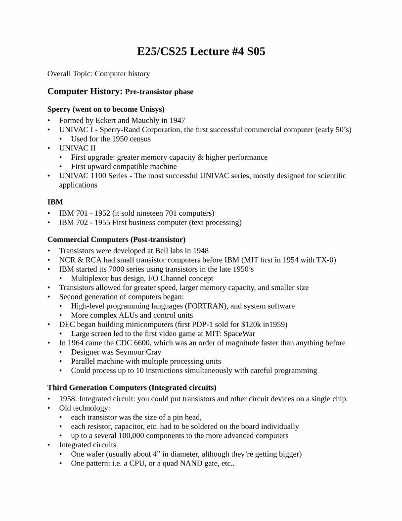
Computer History:
Pre-transistor phase
Sperry (went on to become Unisys)
• Formed by Eckert and Mauchly in 1947• UNIVAC I - Sperry-Rand Corporation, the first successful commercial computer (early 50’s)
• Used for the 1950 census• UNIVAC II
• First upgrade: greater memory capacity & higher performance• First upward compatible machine
• UNIVAC 1100 Series - The most successful UNIVAC series, mostly designed for scientific applications
IBM
• IBM 701 - 1952 (it sold nineteen 701 computers)• IBM 702 - 1955 First business computer (text processing)
Commercial Computers (Post-transistor)
• Transistors were developed at Bell labs in 1948• NCR & RCA had small transistor computers before IBM (MIT first in 1954 with TX-0)• IBM started its 7000 series using transistors in the late 1950’s
• Multiplexor bus design, I/O Channel concept• Transistors allowed for greater speed, larger memory capacity, and smaller size• Second generation of computers began:
• High-level programming languages (FORTRAN), and system software• More complex ALUs and control units
• DEC began building minicomputers (first PDP-1 sold for $120k in1959)• Large screen led to the first video game at MIT: SpaceWar
• In 1964 came the CDC 6600, which was an order of magnitude faster than anything before• Designer was Seymour Cray• Parallel machine with multiple processing units• Could process up to 10 instructions simultaneously with careful programming
Third Generation Computers (Integrated circuits)
• 1958: Integrated circuit: you could put transistors and other circuit devices on a single chip.• Old technology:
• each transistor was the size of a pin head, • each resistor, capacitor, etc. had to be soldered on the board individually• up to a several 100,000 components to the more advanced computers
• Integrated circuits• One wafer (usually about 4” in diameter, although they’re getting bigger)• One pattern: i.e. a CPU, or a quad NAND gate, etc..

• Repeat the pattern in 2D across the chip• Saw the chip into the little blocks• Put each block in a little plastic case with some pins attached• As feature size gets smaller, a linear decrease in feature size in x and y is a squared
increase in the number of components per wafer (wafer cost is the relevant thing)• Current achievements are greater than 200 million transistors in a single chip• IBM System 360 (introduced in 1964)
• First non-upward compatible line, but they wanted to improve the architecture of the 7000 series, and it turned out to be the success of the decade, giving them a 70% market share. • This was IBM’s major move to computers based on integrated circuits
• The 360 architecture is still the basis for most of IBM’s large computers.• The 360 series was the first planned family of machines, with different capabilities for dif-
ferent prices.• 360 was the first multi-tasking architecture with multiple programs stored in memory
• DEC PDP-8• Small enough to sit on a lab bench or be built into other equipment• It was cheap enough for a lab to purchase ($18k).
• PDP-8, followed by the PDP-11, were DEC’s glory years.• PDP series was the first to use a bus architecture.
Memory
• Pre-1970: all memory consisted of metal rings (cores) that could each hold one bit• 1970 - first semiconductor memory of a decent size (256 bits)• 1974 - semiconductor memory became cheaper than core memory (magnetic circles)• 14 generations since 1970:
• 256, 1K, 4K, 16K, 256K, 1M, 4M, 16M, 64M, 256M, 512M, 1G, 2G, 4G
Microprocessors
• First microprocessor was the 4004, which was built by an Intel engineer as the chip to run a calculator for a Japanese firm (he did it on one chip to be more efficient than the 12 requested).• Intel bought back the rights to the chip and came out with the 8008 a few months later• Interest in the chip boomed• The 4004 had 2300 transistors and was a general purpose CPU
• 1974 - Intel 8080, the first general purpose microprocessor, followed by the 8088 and the 8086• 1975 - Wozniak and Jobs design the Apple I using the Morotola 6502 microprocessor• 1977 - Apple II with all the trimmings• 1985 - Intel 80386, their first 32-bit processor (HP, Bell Labs, and Motorola already had one)• 1990 - Intel 80486 and Motorola 68040 have the first on-board float point units [FPU]• 1997 - Pentium II introduces MMX technology (vector processing on a desktop CPU)• 2000 - G4 Altivec introduces a true vector floating point unit to desktop CPUs• 2003 - Itanium goes into production with a revolutionary explicitly parallel architecture• 2005 - Dual core desktop processors

E25/CS25 Lecture #5 S05
Overall Topic: Overall Computer Function
Recent developments in CA
• 64-bit architectures (Itanium, PowerPC 620, UltraSparc, G3/G4/G5)• Vector floating point processors (G4/G5) and floating point SIMD instructions• Threading technology built into the processors
Fetch-Execute Cycle
The fetch-execute cycle is the basis for all computing: fetch the next instruction, execute it.
We can think of this sequence as a state diagram
1. Instruction address calculation - add something to the PC, go through paging & segmentation2. Instruction fetch - read the instruction from the memory location3. Instruction operation decode - figure out what needs to be done4. Operand address calculation - if we need to reference memory, calculate the address5. Operand fetch - fetch the operand from memory or an I/O device6. Data operation - perform the indicated operation on the data7. Operand store - write the result to memory or an I/O device8. Interrupt Pending - check for a pending interrupt and begin interrupt processing if necessary
Added complexities
• OAC state exists multiple times to calculate the address for both load and store operations• There could be multiple operands and multiple results, with multiple memory fetches• Some instructions operate on strings or vectors of numbers
• Repeated operand fetch operations• This is a tighter loop than the entire process since it is a single instruction
Older computers used a simple fetch-execute cycle that executed serially: easy control systems.
Modern computers divide the FE cycle into lots of little pieces (P4 has > 20) and execute multiple instructions in parallel: complex control systems.
Add A + B -> A
Move A -> B
Operand Fetch*
Operand AddressCalculaton*
Instruction Decode
Operand Store*
Instruction AddressCalculation*
Instruction Fetch*
*Could access memory
InterruptPending?

Modern principles of architecture
Do as much of the fetch-execute cycle as possible in hardware, not firmware/software• Make circuits that implement the FE-state machine and control sequences• Alternative is to have microcode, basically an interpreter implemented in a ROM• Note: uCode is flexible
• easier to design and write• adding/changing instructions is easy (i.e. MMX modifications)
Instructions should not take a long time to decode (address calculations should be fast)• Specialized hardware for address calculations• Specialized registers for indexing into memory• Simple instructions of a fixed length• Buffers that keep around the temporary results required to access memory
Reduce references to memory: get rid of memory-based operands as much as possible• Only load and store operations can access memory• No address calculations except on those operations• Have separate input buffers for program instructions and data
• Try to reduce the bottleneck effect of using a Von Neumann architecture
Use lots of registers• Reducing references to memory means you need more registers to hold temporary results• IAS computer had two general purpose registers• Power4 architecture has 32 general purpose integer registers, and 32 floating point regis-
ters, and there are multiple banks of registers on the chip hidden from the architecture

E25/CS25 Lecture #6 S05
Overall Topic: Overall Computer Function
Modern principles of architecture
Pipeline the process• start the next fetch before the current instruction is finished executing• the more steps you have, the more instructions can be started per second•
Superpipelining
: breaking up the F-E pipeline into lots of little steps
Predict Branches• To avoid stalling the pipeline, predict which way branches will go• Requires speculative execution and ability to flush instructions if the prediction is wrong• Lots of branch prediction algorithms, the best ones predict > 95% correct• Randomness in the branching pattern of your code can affect performance
Superscalar design• Have lots of functional units (superscalar design) so that you can achieve processor-level
parallelism and maximize the number of instructions started per second• If you have two integer instructions that don’t depend upon one another, you can execute
them in parallel if you have 2 integer processing units• Requires control circuitry to keep track of what instructions are dependent• Strong dependence between instructions can affect performance• Processors may have two ALUs, a branch unit, a load/store unit, and one or more FPUs• Key is that all of this is hidden from the programmer/user
Use the memory hierarchy to your advantage• The memory hierarchy is a fundamental concept of computer architecture
• As you go up the hierarchy, the cost per bit goes up• As you go down the hierarchy, the size of the memories goes up• Everything is getting faster and cheaper• The most expensive memory is the real estate on the microprocessor itself
• Use fast buffers to hold recently used and/or likely to be used information• Extensive multi-level caching systems• How you access memory in a program affects the performance of the computer
Writing Code for Performance
Both superscalar and memory hierarchy design principles take advantage of the tendences of peo-ple who write code
• There tend to be lots of loops and local accesses• There tend to be different threads of instructions that can execute without interacting
Example of superscalar nice code
for(a long time)a = a + 1;b = b + 1;c = c + 1;

Example of superscalar mean code
for(a long time) a = b + c;b = a + 4;c = b + a;
In the first case, all three instructions in the loop can be executed simultaneously, but in the second case they are all dependent upon the previous instruction.
• There are also at least two “hidden” instructions in the loop• Increment the counter variable• Test for the termination condition
To really stress a computer, you need a string of 6-8 instructions, with each instruction dependent upon the instruction immediately prior to it. This forces serial execution of the code.
A Quick tutorial on cache access
Having a useful memory hierarchy is also dependent upon how we code• Most references are local• Code has a lot of loops• If you use an instruction at location X, you are likely to need the one at X+1
A cache is much, much smaller than main memory
• 64k (2
16
) v. 1G (2
30
)
We need a way to map the memory into the cache
1. Direct-map cache• Think of memory as lots of cache sized blocks (modulo operator)• Byte 1 of each cache-sized block goes to byte 1 of the cache• Byte N of each cache-sized block goes to byte N of the cache• Each memory location has a unique location in the cache defined by the lows bits of the
address
2. 2-way associative mapping• Think of memory as lots of half-cache sized blocks• Byte 1 of each half-cache sized block goes to either byte 0 or byte C/2 of the cache• Byte K of each half-cache sized block goes to either byte K or byte C/2 + K• N-way set-associative means there are N possible cache locations for each memory
address• Several processors use 4-way or 8-way caches to maximize flexibility
Example of memory hierarchy nice code
for(i=0;i<N;i++)do something with a[i]
Each access is sequential across the extent of a[] in memory• A cache line is >> size of an element of a[]• Each time a line is brought from memory, the next k elements of a[] come too• If a[] is < size of cache then all accesses will be from cache after the first pass
• Only memory accesses come at cache line boundaries during the first pass

Example of memory hierarchy mean code
for(i=0;i<N;i+=cache line size) {do something with a[i*size of cache]
If a[] is > cache size, each access will involve going to memory and replacing a line of cache•
Thrashing
is when two conflicting memory locations get called repeatedly
It is possible to write code that is nice to an N-way cache (N > 1) that is mean to a direct-mapped cache
• Don’t access more memory than the cache can hold• Access two (cache size)/2 areas of memory that would conflict in a direct mapped method
Memory
Definitions and characteristics of memories
• Big v. Little Endian:
long integer 0xABCD (or ABGR)• Big Endian: byte 0 is A, byte 1 is B, byte 2 is C, byte 3 is D (ABGR) (0 to 3)
• Lowest byte address is the most significant byte• Little Endian: byte 0 is D, byte 1 is C, byte 2 is B, byte 3 is A (RGBA) (3 downto 0)
• Lowest byte address is the least significant byte• Big Endian: used to be better for comparisons, string or integer• Little Endian: used to be better for addition & subtraction• Big Endian: the number 0xAB_CD_EF_01 is stored as AB_CD_EF_01• Little Endian: the number 0xAB_CD_EF_01 is stored as 01_EF_CD_AB• Endian-ness does not specify the bit ordering within a byte since, from an architectural
point of view, it does not matter so long as operations on the bits follow the convention that accessing the highest bit gives you the most significant bit.

E25/CS25 Lecture #7 S05
Overall Topic: Interrupts and Memory
Interrupts
There is one hiccup that can occur in the Fetch-Execute cycle of a CPU: Interrupts
All CPU’s provide a mechanism whereby outside forces can interrupt the normal processing of the CPU. This is something you have to know about as:
• a system designer: there are often chips that interface between devices and the processor’s interrupt input lines
• an operating system designer: the operating system depends upon interrupts to do house-keeping, handle I/O interfaces, manage memory, and to handle multi-tasking
• an application designer: if you are writing a game, interrupts are one way of giving com-puter time to the bad guys, or of handling your joystick and keyboard input
Classes of interrupts (what should generate interrupts?)• Program: divide by zero, arithmetic overflow, illegal instruction, memory access error• Timer: Allows the operating system to perform certain functions on a regular basis
• vertical retrace manager (60 - 90 times per second)• multi-tasking control• DRAM regeneration (old, old computers)
• Memory: Allows the operating system to manage memory• Certain parts of memory may be on the hard drive (virtual memory)• When the processor needs those parts, it generates a page fault interrupt• The OS handles the page fault and then returns the processor back to its task
• I/O: generated by an I/O device to indicate completion, signal errors, or a need for resources• Floppy drive has a new disk• Someone inserted a CD• You plugged in a USB or firewire device
• Hardware failure: generated when there is a power failure or memory parity error• 200 milliseconds to power off: at 3 GHz you still get 600 million instructions, and maybe
enough power to dump a little information to the hard drive, so what do you do?
Primary purpose of interrupts is to improve efficiency: I/O devices in particular are very slow• Primary use of interrupts is to give the operating system control of the computer
Example of an interrupt• Show sequence with a slow I/O process and no interrrupts
• I/O processing is fast, just get the information from I/O and put it somewhere• Waiting for the next I/O event can take a long time
• Show sequence with a slow I/O process and interrupts• You get a lot more work done this way• You can multi-task

Interrupts and the instruction cycle• Need to add interrupt checking into the basic fetch-execute cycle• Probably want to put it at the end or beginning of instructions (instructions are
atomic
)• Need some element to be atomic, why not instructions?• Then you only need to know the address of the instruction to come back to
• Fetch-execute state diagram includes an interrupt test state prior to the instruction fetch• But what if we having pipelining/superscalar processing going on?• When does the interrupt occur?
What do you do with the current data?• The registers all have data from the current process• The PC points to the next instruction to execute• The stack pointer points to the top of the stack
Normally, the interrupt setup stores only the PC and then puts the interrupt handler address in it• The control unit puts the return address on the stack, and increments the stack pointer• The RTI (Return from Interrupt) instruction pops the address from the stack• It’s up to the interrupt handler to save everything else• The interrupt handler always needs to leave the CPU in the state it found it• Used to save all the registers and such to the stack, the pull them off at the end• Now the CPU often has a small cache for storing the architectural register image
Multiple interrupts• Can handle in sequence by simply turning off interrupts during interrupt handling• Can handle in a hierarchical order, using a priority queue to indicate which interrupts can
interrupt other interrupt handlers.• Turning off some or all interrupts must occur in hardware
• Turning off/on interrupts must be atomic with the interrupt call/return• Otherwise the interrupt could get interrupted with potentially very bad effects
Example: printer (low), disk I/O (middle), network I/O (high)
Instruction set issues:• You may want to be able to generate an interrupt in software• You need to be able to turn interrupts on and off (usually involves setting a flag)• You need to be able to return from an interrupt and enable interrupts in a single atomic
action (otherwise there is time between enabling interrupts and returning from the current interrupt handler)
Finding the interrupt handler address• Interrupt handlers get installed in memory by the OS• Table-based interrupts
• The interrupt handler table has an entry for each type with the handler’s address• On modern machines, this may be cached on the CPU
• Device-based interrupts• Sometimes the CPU queries the device that caused the interrupt• The device returns a memory location for the interrupt handler• On startup, the OS handles getting the driver/interrupt routines set up in the right place

Memory
Definitions and characteristics of memories
• Big v. Little Endian:
long integer 0xABCD (or ABGR)• Big Endian: byte 0 is A, byte 1 is B, byte 2 is C, byte 3 is D (ABGR) (0 to 3)
• Lowest byte address is the most significant byte• Little Endian: byte 0 is D, byte 1 is C, byte 2 is B, byte 3 is A (RGBA) (3 downto 0)
• Lowest byte address is the least significant byte• Big Endian: used to be better for comparisons, string or integer• Little Endian: used to be better for addition & subtraction• Big Endian: the number 0xAB_CD_EF_01 is stored as AB_CD_EF_01• Little Endian: the number 0xAB_CD_EF_01 is stored as 01_EF_CD_AB• Endian-ness does not specify the bit ordering within a byte since, from an architectural
point of view, it does not matter so long as operations on the bits follow the convention that accessing the highest bit gives you the most significant bit.
•
Location
: CPU, Internal (main), External (secondary)• Internal: Registers, L1 cache
• Registers are named one-word/doubleword/quadword storage units• L1 Cache is local copies of small parts of main memory, organized into fixed-size lines• L2 Cache is a larger local memory, now on-chip with all modern processors
• Close by: Main memory (DRAM), L3 cache (SRAM, larger than L2 cache)• Further away: hard disk, CD-ROM, tape
•
Capacity
: usually defined in bytes• From an architecture point of view, memory consists of words or lines• Words might be instruction length or integer length, lines are cache line size• Unit transfer size increases with distance from the computer
•
Cost per bit
: decreases with distance from the computer
•
Unit of transfer
: word, block, line• Bus transfers: word/doubleword/quadword is one piece of data, block is a line of cache, or
a block of memory• Most transfers of memory data are defined in terms of cache lines• page size > blocks/lines > words
•
Access method
: Sequential access, direct access, random access, associative access• tape drive• hard drive/CD• DRAM (both random access and associative access)
•
Addressable Units
: 2
A
= N, where A is the size of the address allowed (usually a word).•
Organization
: How the memory is arranged to form words• A SIMM (single in-line memory module) may have multiple memory chips on it• If consecutive words in memory are alternated among the chips it means you can access
multiple consecutive memory locations simultaneously.•
RAM
: random access memory•
ROM
: read only memory
•
Performance
: access time, cycle time, transfer rate• access time (RAM): time from address presentation to time the data is stored or available

• access time (Direct): time to position the read-write mechanism at the desired location• memory cycle time: amount of time needed to access the same memory block repeatedly• transfer rate: rate at which data can be transferred to or from memory
• RAM: 1 / cycle time• Direct: T
N
= T
A
+ N/R (T
N
: average time to read N bits, T
A
: average access time, N: number of bits, R: transfer rate in bits per second)
•
Physical type
: semiconductor, magnetic surface, optical surface, reflective surface
•
Physical characteristics
: volatile/nonvolatile, erasable/nonerasable• volatile: does the memory decay when the power is turned off?• erasable: can you erase the memory?

E25/CS25 Lecture #8 S05
Overall Topic: Memory
Memory
Definitions and characteristics of memories
• Big v. Little Endian:
long integer 0xABCD (or ABGR)• Big Endian: byte 0 is A, byte 1 is B, byte 2 is C, byte 3 is D (ABGR) (0 to 3)
• Lowest byte address is the most significant byte• Little Endian: byte 0 is D, byte 1 is C, byte 2 is B, byte 3 is A (RGBA) (3 downto 0)
• Lowest byte address is the least significant byte• Big Endian: used to be better for comparisons, string or integer• Little Endian: used to be better for addition & subtraction• Big Endian: the number 0xAB_CD_EF_01 is stored as AB_CD_EF_01• Little Endian: the number 0xAB_CD_EF_01 is stored as 01_EF_CD_AB• Endian-ness does not specify the bit ordering within a byte since, from an architectural
point of view, it does not matter so long as operations on the bits follow the convention that accessing the highest bit gives you the most significant bit.
•
Location
: CPU, Internal (main), External (secondary)• Internal: Registers, L1 cache
• Registers are named one-word/doubleword/quadword storage units• L1 Cache is local copies of small parts of main memory, organized into fixed-size lines• L2 Cache is a larger local memory, now on-chip with all modern processors
• Close by: Main memory (DRAM), L3 cache (SRAM, larger than L2 cache)• Further away: hard disk, CD-ROM, tape
•
Capacity
: usually defined in bytes• From an architecture point of view, memory consists of words or lines• Words might be instruction length or integer length, lines are cache line size• Unit transfer size increases with distance from the computer
•
Cost per bit
: decreases with distance from the computer
•
Unit of transfer
: word, block, line• Bus transfers: word/doubleword/quadword is one piece of data, block is a line of cache, or
a block of memory• Most transfers of memory data are defined in terms of cache lines• page size > blocks/lines > words
•
Access method
: Sequential access, direct access, random access, associative access• tape drive• hard drive/CD• DRAM (both random access and associative access)
•
Addressable Units
: 2
A
= N, where A is the size of the address allowed (usually a word).•
Organization: How the memory is arranged to form words• A SIMM (single in-line memory module) may have multiple memory chips on it• If consecutive words in memory are alternated among the chips it means you can access
multiple consecutive memory locations simultaneously.

• RAM: random access memory• ROM: read only memory
• Performance: access time, cycle time, transfer rate• access time (RAM): time from address presentation to time the data is stored or available• access time (Direct): time to position the read-write mechanism at the desired location• memory cycle time: amount of time needed to access the same memory block repeatedly• transfer rate: rate at which data can be transferred to or from memory
• RAM: 1 / cycle time• Direct: TN = TA + N/R (TN: average time to read N bits, TA: average access time, N:
number of bits, R: transfer rate in bits per second)
• Physical type: semiconductor, magnetic surface, optical surface, reflective surface
• Physical characteristics: volatile/nonvolatile, erasable/nonerasable• volatile: does the memory decay when the power is turned off?• erasable: can you erase the memory?
Physical Makeup of Main Memory
Originally core memory (doughnut-shaped magnetic loops)
Now all Si
• Most semiconductor memory is random access (directly addressable)• associative memory is in the research stage
RAM - typical name for volatile memory• Existing non-volatile memories are not fast enough to be main memory elements
Static RAM [SRAM] - made with flip-flops, will hold its state as long as power is supplied• Aside: SRAM doesn’t take much power. CMOS technology only uses current when the
gates switch states. So, if you don’t access the SRAM it really doesn’t use any current. Thus, you can keep information in SRAM for a long time using a very small battery (most computers do have a small SRAM cache that runs the clock, and other system parameters).
Dynamic RAM [DRAM] - made with capacitors. Imagine trying to store information as rows of leaky buckets. Every once in a while you have to refill the buckets that are supposed to represent high voltage values (1).
• DRAM can be denser than SRAM because each bit only needs a capacitor• DRAM needs refresh circuitry that updates the values in each capacitor on a regular basis• The goal of DRAM designers is to reduce the size of the capacitor and increase the sensi-
tivity of reading mechanism so that the presence of a single electron indicates whether that memory location is a 1 or a 0.
Magnetic RAM [MRAM] - in research stage at Motorola and elsewhere. Idea is to have a transis-tor that can be magnetized to be on or off (storing a 1 or a zero). MRAM is non-volatile, as fast as SRAM, and as compact as DRAM.
Pretty much all main computer memories are DRAM because of its bit density• SRAM is used largely in caches since it is faster and does not need to be refreshed

Main Memory [DRAM] Design
• SDRAM: Synchronous DRAM (e.g. 100 MHz memory bus or faster)• RAM accesses are synchronized with a clock• Like DRAM, can use a burst mode where it sends a consecutive block of memory• Latencies are given in clock cycles: 5-1-1-1 (5 cycles after row address, 1 per column)• Cheap to make, build, and use
• CDRAM: Cache DRAM, or Enhanced SDRAM• The DRAM SIMM itself contains an SRAM cache that holds at least the last block of
memory accessed, if not more.• DRDRAM Direct Rambus DRAM
• Packet based protocol rather than RAS/CAS style access• Very strict standard for physical placement of the memory and bus design• The high-end version has two channels between the processor and memory• RDRAM has held on, but the cheaper, open design DDR SDRAM is competitive• RAMBUS had higher a higher bandwidth than standard SDRAM, but also higher latencies
than SDRAM• The original RAMBUS was only 16 bits wide, and ran at 800MHz• The new XDR Rambus interface is still 16 bits wide, but runs at 3.2GHz (6.4GB/s path)
• DDR SDRAM (Double data rate SDRAM)• Also contains two channels to the memory• 400Mb/s and 533Mb/s speeds are out
• Athlon64 3400+ supports the 400 spec• Each bus is 64-bits wide
• At 400Mb/s x 8 bytes wide = 3.2GB/s data path, 533 means 4.3GB/s• RLDRAM: Reduce Latency DRAM, basically faster DDR SDRAM, smaller bus width.
Non-volatile memories
ROM - read-only memory• manufacture the information into the chip• better not make a mistake
PROM - programmable ROM• can be written once (blowing fuses with a high voltage)
EPROM - erasable ROM• shine a UV light on it and it disperses the charge• can program it electronically using a high voltage
EEPROM - electrically erasable ROM• Can erase a byte or a block using a high voltage• Can program electronically
Flash memory• Program electronically, and erase a block of memory in 1-2 seconds using a high voltage
Note: Harvard v. Von Neumann architecture (separate v. same data & instruction memory) relates to this topic. On a microcontroller you can have physically different memories for data & program if you have a Harvard architecture, but not if you have a Von Neumann architecture.

Memory Hierarchy Design
• First computers had two levels of main memory• Small number of internal registers• Larger amount of RAM located off-chip
• Next generation had more internal registers to hold temporary results.
• Current generation of computers add up to three levels to this hierarchy• Level 1 cache: on-chip, small (but much larger than # of registers), 8-32k• Level 2 cache: used to be off-chip, but not now on most CPUs, 96k-8M• Level 3 cache: off-chip in between the DRAM and the level 2 cache, 2-4M or more
All of these developments help you because of the principle of locality of reference• Cost, capacity, and access time are driven by technology• You want to have the biggest, cheapest, fastest memory possible
• But: bigger memories are slower• But: cheaper memory is slower• But: faster memory is much more expensive and usually much smaller
• Can you have some combination of small fast memory and big slow memory that acts like a cheap, big, fast memory?
Locality of reference makes using multiple kinds of memory useful
Locality of Reference
If all addresses are equally likely to be addressed at all times, then using intermediate levels can slow you down. Fortunately, this is not the case.• In the short run (temporal locality), memory accesses tend to cluster
• program execution is sequential except for branch and call commands (10-20 %)• recursion without many instructions in between calls and returns is rare• most programs work within a narrow depth of procedure calls• most iterative constructs consist of a relatively small number of instructions• in many programs, data consists of organized blocks, structures, or arrays
• Over the long run they can change significantly• An appropriately structured memory hierarchy can significantly decrease the number of
accesses necessary to the lower (slower) levels of memory• In short stretch of code (spatial locality), memory accesses tend to cluster
• Need to balance how much memory you bring in at a time (cache line size) with the cost of bringing in too much (likelihood that you’ll need all of it)

E25/CS25 Lecture #9 S05
Overall Topic: Memory and cache
Main Memory [DRAM] Design
• SDRAM: Synchronous DRAM (e.g. 100 MHz memory bus or faster)• RAM accesses are synchronized with a clock• Like DRAM, can use a burst mode where it sends a consecutive block of memory• Latencies are given in clock cycles: 5-1-1-1 (5 cycles after row address, 1 per column)• Cheap to make, build, and use
• CDRAM: Cache DRAM, or Enhanced SDRAM• The DRAM SIMM itself contains an SRAM cache that holds at least the last block of
memory accessed, if not more.• DRDRAM Direct Rambus DRAM
• Packet based protocol rather than RAS/CAS style access• Very strict standard for physical placement of the memory and bus design• The high-end version has two channels between the processor and memory• RDRAM has held on, but the cheaper, open design DDR SDRAM is competitive• RAMBUS had higher a higher bandwidth than standard SDRAM, but also higher latencies
than SDRAM• The original RAMBUS was only 16 bits wide, and ran at 800MHz• The new XDR Rambus interface is still 16 bits wide, but runs at 3.2GHz (6.4GB/s path)
• DDR SDRAM (Double data rate SDRAM)• Also contains two channels to the memory• 400Mb/s and 533Mb/s speeds are out
• Athlon64 3400+ supports the 400 spec• Each bus is 64-bits wide
• At 400Mb/s x 8 bytes wide = 3.2GB/s data path, 533 means 4.3GB/s• RLDRAM: Reduce Latency DRAM, basically faster DDR SDRAM, smaller bus width.
Non-volatile memories
ROM - read-only memory• Manufacture the information into the chip• Better not make a mistake
PROM - programmable ROM• Can be written once (blowing fuses with a high voltage)
EPROM - erasable ROM• Shine a UV light on it and it disperses the charge• Can program it electronically using a high voltage
EEPROM - electrically erasable ROM• Can erase a byte or a block using a high voltage and program it electronically
Flash memory• Program electronically, and erase a block of memory in 1-2 seconds using a high voltage

Note: Harvard v. Von Neumann architecture (separate v. same data & instruction memory) relates to this topic. On a microcontroller you can have physically different memories for data & program if you have a Harvard architecture, but not if you have a Von Neumann architecture.
Memory Hierarchy Design
• First computers had two levels of main memory• Small number of internal registers• Larger amount of RAM located off-chip
• Next generation had more internal registers to hold temporary results.
• Current generation of computers add up to three levels to this hierarchy• Level 1 cache: on-chip, small (but much larger than # of registers), 8-32k• Level 2 cache: used to be off-chip, but not now on most CPUs, 96k-8M• Level 3 cache: off-chip in between the DRAM and the level 2 cache, 2-4M or more
All of these developments help you because of the principle of locality of reference• Cost, capacity, and access time are driven by technology• You want to have the biggest, cheapest, fastest memory possible
• But: bigger memories are slower• But: cheaper memory is slower• But: faster memory is much more expensive and usually much smaller
• Can you have some combination of small fast memory and big slow memory that acts like a cheap, big, fast memory?
Locality of reference makes using multiple kinds of memory useful
Locality of Reference
If all addresses are equally likely to be addressed at all times, then using intermediate levels can slow you down. Fortunately, this is not the case.• In the short run (temporal locality), memory accesses tend to cluster
• program execution is sequential except for branch and call commands (10-20 %)• recursion without many instructions in between calls and returns is rare• most programs work within a narrow depth of procedure calls• most iterative constructs consist of a relatively small number of instructions• in many programs, data consists of organized blocks, structures, or arrays
• Over the long run they can change significantly• An appropriately structured memory hierarchy can significantly decrease the number of
accesses necessary to the lower (slower) levels of memory• In short stretch of code (spatial locality), memory accesses tend to cluster
• Need to balance how much memory you bring in at a time (cache line size) with the cost of bringing in too much (likelihood that you’ll need all of it)
Cache Memory
We want to give memory the speed of the fastest memory possible (approximately the speed of the fastest memory available)
We don’t want it to cost too much (approximately the cost of the cheapest memory available)

Example: main memory, and a much faster cache
• cache contains portions of main memory
• when the CPU attempts to read a word, it checks the cache for the word• if there, it gets the word quickly• if not there, a block of memory containing that word gets moved into the cache, & the
CPU gets the word• locality of reference makes it likely that the next word the CPU wants will be in the cache
• Hit ratio H is the percentage of time the memory you want is in the cache• Ts = T1 + (1 - H) * T2• Ts = average access time• T1 = speed of faster memory• T2 = speed of slower memory
Definitions
• Memory is divided into M equal size blocks of W words each, M = 2n / W
• A cache consists of C lines or blocks of W words• C << M• Each block has a tag that identifies where it came from
(usually a portion of the memory address)
• Cost per bit:
• C1 = cost per bit of level 1 memory, S1 = size of level 1 memory• C2 = cost per bit of level 2 memory, S2 = size of level 2 memory
• Example: • 512MB DRAM costs $100 = 2.33 e-6 cents / bit• 64k cache costs $20 = 0.03 cents/bit
• ~20% increase in cost/bit for a 0.012% increase in size
Cs
C1S1 C2S2+
S1 S2+-------------------------------=
Cs$100 $20+
232
219
+---------------------------- 2.79
6–×10= =

E25/CS25 Lecture #10 S05
Overall Topic: Cache
Mapping Function:
Example is 64Kbyte (216) cache, organized into blocks of 8 bytes, so there are 8K lines (213) of 8 bytes each. Main memory is 1G (230), or 16M of 8-byte blocks/lines. Use 32-bit addresses.• Direct Mapping
• Each block of main memory maps to a single line of cache. • i = j mod m, where i = cache line number, j = main memory block number, and m = num-
ber of lines in cache.• The least significant w (in this case 3) bits identify a unique word or byte within a block of
main memory. The remaining s bits specify a block of memory (in this case 29). There are
2r lines of cache (r = 13 in this case), so there are s-r bits remaining for the tag field. These s-r bits are the most significant bits in the address.
• The top s-r (16) bits are saved as the tag for a line of cache• The middle r (13) bits specify which line of cache that block maps into• The low w (3) bits specify which word or byte within the block is being addressed• Advantage is efficiency & simplicity of implementation• Disadvantage is there is a fixed cache location for any given block
• Associative Mapping• Any block can be loaded into any line of cache• Address is interpreted as a tag (29) and a word field (3)• tags have to be compared in parallel to determine if a particular block is in the cache• Flexible but hard to implement because of the circuitry
• Set Associative Mapping• Divide the cache into v sets, each of which contains k lines.• m = v x k (m = number of lines in cache, v = sets, k = number of lines per set)• i = j modulo v (i = cache set number, j = main memory block number, v = # sets)• A block of memory can be mapped to any of the k lines in each set• Address is interpreted as 3 fields: tag, set, word
• d set bits specify one of v = 2d sets• s bits of the tag & set fields specify a block of memory
• Example of two-way set associative (2 lines per set)
• 212 sets, 23 words per line, 217 blocks map to each set• 2 lines per set is typical, 4 or 8 lines gives a little better performance• more than that gives marginal improvement, but increases the complexity of the design
Key to understanding the breakdown in memory addresses is a tag/set/word diagram
Tag Set or Line Word
# of bits required toaccess a unit in a line
# of bits required toselect a set or line
# remaining bits of the addressindicating source of the line

Replacement Algorithms in associative caches• Least-recently used: 2-way SA: flag a line if it’s been used and set the other to 0• FIFO: round-robin using a circular buffer counter indicating last used line• Least-frequently used: put a counter on each line of cache• Approximate LRU: (486 style) tree with 1 bit indicating most recent usage at each branch
Write Policy• Write-through - all writes made to memory. Other modules connected to the bus can watch the
bus transactions and invalidate their own lines of cache if they see that line being transferred to main memory. On average, writes make up 15% of bus traffic.
• Write-back - set an update bit in the cache, when the block is replaced then write it to main memory (or at least the level above) if it’s been updated. Need to be careful about coherency. All reads go through the cache, which can create bottlenecks.
Other cache issues
Multiple processor write policies• Bus snooping, assuming a write-through protocol• Hardware transparency - a write is automatically
distributed to various caches• Non-cachable memory - shared memory cannot be
cached (is always a miss)
Block Size• larger blocks reduce the number of blocks in
cache, causes more overwrites• in larger blocks, the more distant words are not needed as often• 8 to 32 bytes or addressable units per block seems reasonably close to optimum for desk-
top machines, 64-128 byte lines are good for high-performance computers.
Number of caches: Single v. Two v. Three-level Caches• As the caches move onto the chip or into the package, computer manufacturers continue to
add levels of cache• Cache coherence is the main tradeoff for the speed gains, and it means extra hardware• The hit rate on the higher levels of cache needs to be high, or they’re not worth having
• If your hit rate for level 1 and for level 2 is 70%, then you would only have a miss to level 3 on ~10% of memory accesses
• If your hit rate for level 3 is also 70%, then 7/100 accesses would be to level 3 cache, and 3/100 would be to main memory instead of 10/100.
• If main memory takes 2x as long as level 3, you get a small improvement: 20 v. 13 time units for the 10 accesses. (SDRAM latency is 2-2.5 clock cycles, L3 latency is 1 clock cycle)
• If there is an SRAM cache already in the DRAM chip, do you need a level 3 cache?
Unified v. Split Cache• Unified cache holds both data and instructions• A unified cache automatically provides flexibility in distributing the cache between
instructions & data
CPUMemory
I/O Devices
Buses
cache

• A unified cache can slow down new superscalar processors which are looking ahead to the next instruction while the current one is being processed. A read from cache for implent-ing the current instruction blocks access to the next instruction.
• A split cache means there is one cache for instructions (read-only) and one cache for data (read and write).
• Different parts of the processor can access memory at the same time with a split cache• There is less flexibility with split cache, but it supports pipeline processing better
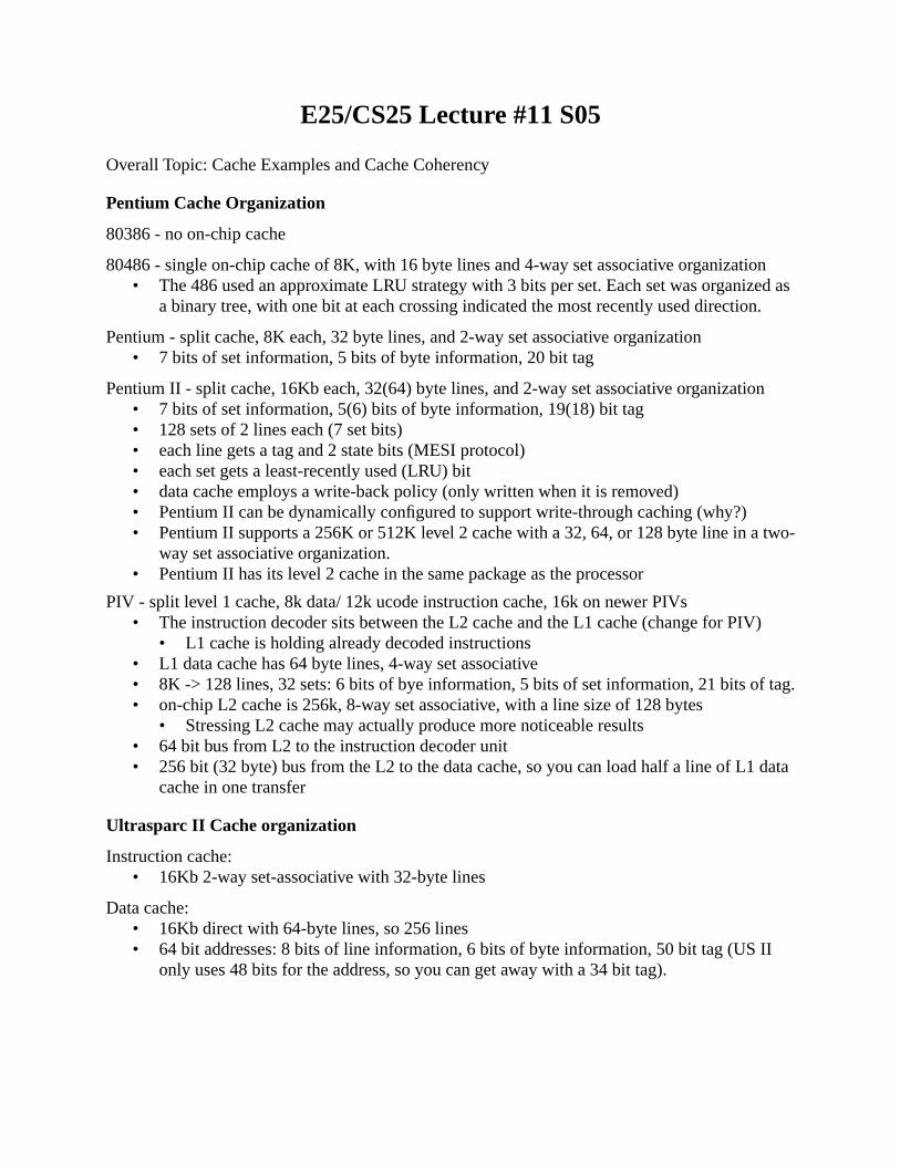
Pentium Cache Organization
80386 - no on-chip cache
80486 - single on-chip cache of 8K, with 16 byte lines and 4-way set associative organization• The 486 used an approximate LRU strategy with 3 bits per set. Each set was organized as
a binary tree, with one bit at each crossing indicated the most recently used direction.
Pentium - split cache, 8K each, 32 byte lines, and 2-way set associative organization• 7 bits of set information, 5 bits of byte information, 20 bit tag
Pentium II - split cache, 16Kb each, 32(64) byte lines, and 2-way set associative organization• 7 bits of set information, 5(6) bits of byte information, 19(18) bit tag• 128 sets of 2 lines each (7 set bits)• each line gets a tag and 2 state bits (MESI protocol)• each set gets a least-recently used (LRU) bit• data cache employs a write-back policy (only written when it is removed)• Pentium II can be dynamically configured to support write-through caching (why?)• Pentium II supports a 256K or 512K level 2 cache with a 32, 64, or 128 byte line in a two-
way set associative organization.• Pentium II has its level 2 cache in the same package as the processor
PIV - split level 1 cache, 8k data/ 12k ucode instruction cache, 16k on newer PIVs• The instruction decoder sits between the L2 cache and the L1 cache (change for PIV)
• L1 cache is holding already decoded instructions• L1 data cache has 64 byte lines, 4-way set associative• 8K -> 128 lines, 32 sets: 6 bits of bye information, 5 bits of set information, 21 bits of tag.• on-chip L2 cache is 256k, 8-way set associative, with a line size of 128 bytes
• Stressing L2 cache may actually produce more noticeable results• 64 bit bus from L2 to the instruction decoder unit• 256 bit (32 byte) bus from the L2 to the data cache, so you can load half a line of L1 data
cache in one transfer
Ultrasparc II Cache organization
Instruction cache: • 16Kb 2-way set-associative with 32-byte lines
Data cache:• 16Kb direct with 64-byte lines, so 256 lines• 64 bit addresses: 8 bits of line information, 6 bits of byte information, 50 bit tag (US II
only uses 48 bits for the address, so you can get away with a 34 bit tag).

Ultrasparc III Cache organization
Instruction cache (L1):• 32 kB 4-way set-associative
Data cache:• 64 kB 4-way set-associative
Load-store unit:• 2 kB prefetch• 2 kB Write
L2-cache Tag RAM and controller on-chip to support 1, 2, or 8 MB external• Why put the tags on the chip?
PowerPC Cache Organization• 601: 32K unified cache, 32 bytes/line, 8-way SA• 603: 16K split cache (8K each), 32 bytes/line, 2-way SA• 604: 32K split cache (16K each), 32 bytes/line, 4-way SA• G3: 64K split cache (32K each), 64 bytes/line, 8-way SA• G4: 64K split cache (32K each), 32 bytes/line, both 8-way SA
• one-die L2 cache is 256K to 1M, pipelined, and 8-way SA• supports L3 cache up to 2MB, with a 64-bit bus width
• G5: 64K, direct mapped I-cache, 32K, 2-way D-cache, 128 bytes/line • 512K 8-way L2 cache• Note I-cache is larger than D-cache• RISC designs generally have more instructions than CISC designs• G5 has no L3 cache• 800-1000MHz bus speeds, 42-bit buts, and transfer rates of 6.4GB/s
E25/CS25 Lecture #11 S05
Overall Topic: Cache Examples and Cache Coherency
Pentium Cache Organization
80386 - no on-chip cache
80486 - single on-chip cache of 8K, with 16 byte lines and 4-way set associative organization• The 486 used an approximate LRU strategy with 3 bits per set. Each set was organized as
a binary tree, with one bit at each crossing indicated the most recently used direction.
Pentium - split cache, 8K each, 32 byte lines, and 2-way set associative organization• 7 bits of set information, 5 bits of byte information, 20 bit tag
Pentium II - split cache, 16Kb each, 32(64) byte lines, and 2-way set associative organization• 7 bits of set information, 5(6) bits of byte information, 19(18) bit tag• 128 sets of 2 lines each (7 set bits)• each line gets a tag and 2 state bits (MESI protocol)• each set gets a least-recently used (LRU) bit• data cache employs a write-back policy (only written when it is removed)• Pentium II can be dynamically configured to support write-through caching (why?)• Pentium II supports a 256K or 512K level 2 cache with a 32, 64, or 128 byte line in a two-
way set associative organization.• Pentium II has its level 2 cache in the same package as the processor
PIV - split level 1 cache, 8k data/ 12k ucode instruction cache, 16k on newer PIVs• The instruction decoder sits between the L2 cache and the L1 cache (change for PIV)
• L1 cache is holding already decoded instructions• L1 data cache has 64 byte lines, 4-way set associative• 8K -> 128 lines, 32 sets: 6 bits of bye information, 5 bits of set information, 21 bits of tag.• on-chip L2 cache is 256k, 8-way set associative, with a line size of 128 bytes
• Stressing L2 cache may actually produce more noticeable results• 64 bit bus from L2 to the instruction decoder unit• 256 bit (32 byte) bus from the L2 to the data cache, so you can load half a line of L1 data
cache in one transfer
Ultrasparc II Cache organization
Instruction cache: • 16Kb 2-way set-associative with 32-byte lines
Data cache:• 16Kb direct with 64-byte lines, so 256 lines• 64 bit addresses: 8 bits of line information, 6 bits of byte information, 50 bit tag (US II
only uses 48 bits for the address, so you can get away with a 34 bit tag).

Ultrasparc III Cache organization
Instruction cache (L1):• 32 kB 4-way set-associative
Data cache:• 64 kB 4-way set-associative
Load-store unit:• 2 kB prefetch• 2 kB Write
L2-cache Tag RAM and controller on-chip to support 1, 2, or 8 MB external• Why put the tags on the chip?
PowerPC Cache Organization• 601: 32K unified cache, 32 bytes/line, 8-way SA• 603: 16K split cache (8K each), 32 bytes/line, 2-way SA• 604: 32K split cache (16K each), 32 bytes/line, 4-way SA• G3: 64K split cache (32K each), 64 bytes/line, 8-way SA• G4: 64K split cache (32K each), 32 bytes/line, both 8-way SA
• one-die L2 cache is 256K to 1M, pipelined, and 8-way SA• supports L3 cache up to 2MB, with a 64-bit bus width
• G5: 64K, direct mapped I-cache, 32K, 2-way D-cache, 128 bytes/line • 512K 8-way L2 cache• Note I-cache is larger than D-cache• RISC designs generally have more instructions than CISC designs• G5 has no L3 cache• 800-1000MHz bus speeds, 42-bit buts, and transfer rates of 6.4GB/s
Cache Coherency
To provide cache consistency, many computers support a protocol known as MESI• PowerPC architecture• Pentium architecture• MIPS architecture
MESI = modified/exclusive/shared/invalid
MESI supports mutiple processor systems, each with multiple levels of cache• MESI is a write-once, snooping protocol
Data cache needs to have 2 bits per tag (line) so each line can have 4 states• modified: the line in the cache has been modified and is only available in this cache• exclusive: the line in the cache is the same as the memory level above and is not present in
any other cache• shared: the line in the cache is the same as the level above and may be present in other
caches• invalid: the line in the cache does not contain valid data

L1 MESI protocol1. Cache line begins in the invalid state2. Data is retrieved from main memory, stored in L2, and the L1.
• The state of the line is Shared if any other cache has a copy (L2 does)• A read operation does not invalidate the line in other caches• The bus on a MESI CPU must have an additional “shared” line that is a wired-OR
3. If the CPU writes to the cache line, the cache line in the L1 cache gets updated• The first time it is updated, the line also gets written to the L2 cache• The state of the L1 line is changed to Exclusive.• Before the write can take place, however, a Read-Exclusive bus transaction from main
memory has to take place. This notifies all other caches that the line is invalid.• The read exclusive operation invalidates the line in other processors’ caches
4. If the CPU writes to this line again, then the L1 line gets marked as Modified, and remains in this state. The data is NOT moved to the L2 cache. This is a write-once policy.
5. When it is necessary to replace a line in the L1 cache, if that line is in the S or E state it need not be written out. If the line is in the M state, the line is written back to the L2 cache and then flushed from the L1 cache. The new data is marked as Shared in the L1 cache.
L2 MESI protocol1. The L2 cache begins in the S or E state when it reads a block from main memory and passes
the block to the L1 cache. • This block is exclusive to this L1/L2/processor module if no other caches have it• The shared line on the bus lets the L2 cache know if the data is shared by another
2. When a write-once occurs, the L2 updates the line and puts it in the M state. The L2 cache is not notified of any further updates.• If the data is shared, the L2 must use a Read-Exclusive transaction before the writes occur.• The Read-Exclusive transaction invalidates that data in all other caches
3. If another bus master attempts to read that line, and the line is not in the shared or exclusive state, then the L2 cache blocks the transaction and passes the address to its processor. • If the L1 line is in an exclusive state, then L2 can perform the write-back cycle to main
memory, while simultaneously providing the data to the other cache.• If the L1 line is in a modified state, then the system performs a write-back cycle all the
way from L1 to update main memory.• The L2 cache then releases the bus to perform its read operation.
4. If another bus master attempts to write data in that line, the L2 again blocks the transaction. The L2 must put the actions in the proper sequence.• The L2 cache detects and blocks the write operation• The L2 cache signals its L1 cache with the address of the write operation.• If the L1 cache is in a modified state
• It performs a write-through from L1 to main memory.• The L1 and L2 cache lines are then invalidated (because data is being written to that
main memory block by another component)• If the L1 cache is is in an exclusive state
• The L2 cache performs a write to main memory and invalidates the L1 and L2 lines.• The L2 cache releases the bus master and allows it to complete the transaction
On the Pentium, 2 bits of a control register determine the write-policy for the cache

Magnetic Disk Organization
• Head - coil of wire (electromagnet) can both read and write (sense current, or drive current)• Platter - covered with magnetic material, spinning at a constant speed
• Platter is organized into concentric rings - Tracks• Tracks are separated by gaps to reduce errors• Same # of bits per track, and constant angular velocity [CAV]
• Density is higher on the inside tracks (like an LP)• Each track is composed of sectors separated by gaps• Sectors are pre-formatted with information like a synchronization code, ID numbers, and
control information• Each sector contains a certain amount of data, and space for an error-correcting code
• Old drives had same # sectors/track for the entire disk• Modern disks divide the tracks into zones; same # of sectors/track within a zone
Characteristics of Magnetic Disks• Movable (1 head) v. fixed heads (1 head/track)• Nonremovable v. removable disks• double-sided v. single sided• multiple platters v. single platter
• In 2001 a 1” high 40GB drive could have 6 platters running at 10,000 RPM• In 2003 a 1” high 40GB drive could have 4 double-sided platters at 15,000 RPM• In 2004 a 1” high 40GB drive could have 2 double-sided platters at 15,000 RPM
• A 1” high 200GB drive could have 2 double-sided platters at 7200 RPM• air gap head (older disk drives), contacting head (floppy drives), Winchester drives
• Winchester drives first designed by IBM• Sealed package created in a low contaminant environment• When the disk is stopped, the disk head (an aerodynamic foil) rests on the surface• When the disk is spinning, the foil holds the head just above the surface• The Winchester drive heads can be much smaller than an air gap or contacting head• Most drives today are Winchester drives
• Current disk drives use separate read and write heads (positioned very close)• The write is a doughnet with the bottom removed and a small wire coil• The read head is a magnetoresistive material that changes resistance in response to
changes the surrounding magnetic field
E25/CS25 Lecture #12 S05
Overall Topic: RAID
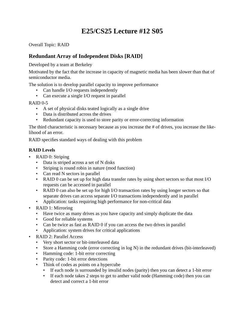
Redundant Array of Independent Disks [RAID]
Developed by a team at Berkeley
Motivated by the fact that the increase in capacity of magnetic media has been slower than that of semiconductor media.
The solution is to develop parallel capacity to improve performance• Can handle I/O requests independently• Can execute a single I/O request in parallel
RAID 0-5• A set of physical disks teated logically as a single drive• Data is distributed across the drives• Redundant capacity is used to store parity or error-correcting information
The third characteristic is necessary because as you increase the # of drives, you increase the like-lihood of an error.
RAID specifies standard ways of dealing with this problem
RAID Levels• RAID 0: Striping
• Data is striped across a set of N disks• Striping is round robin in nature (mod function)• Can read N sectors in parallel• RAID 0 can be set up for high data transfer rates by using short sectors so that most I/O
requests can be accessed in parallel• RAID 0 can also be set up for high I/O transaction rates by using longer sectors so that
separate drives can access separate I/O transactions independently and in parallel• Application: tasks requiring high performance for non-critical data
• RAID 1: Mirroring• Have twice as many drives as you have capacity and simply duplicate the data• Good for reliable systems• Can be twice as fast as RAID 0 if you can access the two drives in parallel• Application: system drives for critical applications
• RAID 2: Parallel Access• Very short sector or bit-interleaved data• Store a Hamming code (error correcting in log N) in the redundant drives (bit-interleaved)• Hamming code: 1-bit error correcting• Parity code: 1-bit error detections• Think of codes as points on a hypercube
• If each node is surrounded by invalid nodes (parity) then you can detect a 1-bit error• If each node takes 2 steps to get to anther valid node (Hamming code) then you can
detect and correct a 1-bit error

• Can be set up for high transfer rates (small sectors), but not really for parallel access• Application: not offered commercially
• RAID 3• Very short sector or bit interleaved• One extra disk which contains the parity for the data striped across the disks• Very fast parallel access• Application: imaging, CAD design, one application accessing lots of data
• RAID 4: Independent access• Long sectors for high I/O transaction rates• Parity bits in one extra drive• Problem is that all reads and writes must still use the parity disk even for independent par-
allel transactions (but easy to fix crashes)• Application: not offered commercially

E25/CS25 Lecture #13 S05
Overall Topic: RAID
Redundant Array of Independent Disks [RAID]
• RAID 1-4 Summary• RAID 0: striping across disks (set up for parallel or independent accesses)• RAID 1: mirroring (set up for parallel or independent accesses)• RAID 2: Parallel access with Hamming code• RAID 3: Parallel access with a single parity disk• RAID 4: Independent access with a single parity disk
• RAID 5: Independent access• Long sectors for high I/O transaction rates• Both data and parity information is interleaved among all of the disks• Removes the bottleneck of the last disk, but makes crashes more complex• Two disks have to fail in the mean time to repair [MTTR] to lose data• Application: High request rate, read intensive, data lookup (Database servers)
• RAID 6: Independent access• Long sectors for high I/O transaction rates• Two independent parity checks
• One is a standard XOR parity, the other is an independent 1-bit check• In one implementation, the 2nd parity is a copy of the first parity• In another implementation, the 2nd parity is a vertical parity v. horizontal parity
• Data sectors, parity, and second parity are interleaved across disks• Three disks have to fail in the MTTR to lose data (accordingt to the manufacturer)• Application: tasks requiring anytime access
• RAID 10: Striped information built on mirrored drives• The overall configuration is striped with no redundancy• Each “individual drive” is actually a RAID 1 system with mirroring
• RAID 53: Striped parity on fast transfer devices• The overall configuration is striped parity (RAID 5)• Each “individual drive” is actually a RAID 3 system (fast transfer with parity)
Review for Exam

E25/CS25 Lecture #14 S05
Overall Topic: Buses
Interconnection structures: The Bus
What kinds of information must a bus carry?
• data lines• the number of data lines is defined as the width of the bus: 1 line = 1 bit
• address lines• typically, high order bits select modules (I/O devices)• low order bits select ports or memory locations within the module (I/O devices)
• control lines• specify who gets to put stuff on the bus, who’s supposed to read it, and what they’re sup-
posed to do with it• Process of who gets control is called arbitration
• arbitration can be centralized (bus controller) or distributed (competitive process)• Example control lines
• Memory write: data to be written to the address• Memory read: data to be placed on the bus from the address• I/O write: data to be written to the I/O device• I/O read: I/O data to be placed on the bus• Transfer ACK: transfer acknowledged, indicates data has been read or placed on bus• Bus request: flag indicating a module needs the bus• Bus grant: flag indicating that module has control of the bus• Interrupt request: indicates that an interrupt is pending• Interrupt ACK: acknowledge that the pending interrupt has been recognized• Clock: synchronizes operations• Reset: initialize all modules
Using the bus to write
1. The module must obtain use of the bus2. The module must put the data on the bus and set the appropriate control & address lines3. wait for the acknowledge signal before relinquishing the bus
Using the bus to read
1. Obtain use of the bus2. transfer a request to another module to place data on the bus (address & control lines)3. wait for the acknowledge signal from the second module4. read the data
For clocked buses, all devices on the bus must be able to follow the protocol for communication • Obtaining the use of the bus can be done in parallel with the previous data transaction• Clocked buses do not require acknowledgements (but may use them in some cases)

Multiple-bus hierarchies
As you add devices to a bus, performance will suffer
1. The more devices trying to use the bus, the longer the delay in gaining access.• Especially true when control changes frequently
2. The bus can be a bottleneck when the data transfer demand starts to approach the capacity of the bus (average transfer speed * number of data lines).
To solve this problem, most systems use a multiple-bus hierarchy
• Internal bus between the processor and cache memory• All on-chip now, and very high bandwidth• Latest PIV has 2MB L3 cache on the chip!
• System bus/local bus between the cache and a memory bridge• Expansion bus (backplane) connecting I/O devices to the memory bridge• The I/O Bridge connects the different buses and can buffer communication between them.
Bridges allow for different bus clocks, processors, and I/O devices to all use the same architecture
Intel is currently pushing PCI Express as a new model for computer bus architectures• Model is a switch rather than a hub
• Devices can talk to one another directly rather than going through a buffer• “Lanes” can be added as necessary to accommodate bandwidth• Devices that don’t need memory can trade information without going through a bridge
Many bus designs are moving away from parallel wires with a slow clock speed to a small number of wires (even 1) with much faster clock speeds
• Faster communication over distances• Simpler electronics• Simpler physical interconnections for consumer ease of use (think USB v. SCSI)
Design Options• Bus type
• Dedicated• bus lines are used for one purpose only: faster but more wires
• Multiplexed• bus lines are used for multiple purposes: slower but fewer wires• serial buses are all multi-plexed because 1 wire serves all three functions
• Pipelined (PII bus has 5 states: Req / Error / Snoop / Resp / Data)
CPU MemoryBridge
Graphics
Memory
I/OBridge
HardDrives
USB Hub
Local I/O
PCI bus
Network Firewire
AGP ATA
SystemBus
Cacheschipset

• Method of arbitration• Centralized: one chip makes all of the bus master decisions or a daisy chain solution• Distributed: devices duke it out based on location or an ID number
• Example: daisy-chaining a voltage signal, so priority is in order of connection• Timing
• synchronous• a master clock runs the bus; it has to match the slowest device• only requires partial handshakes (don’t have to say “I got it”)
• asynchronous• runs at the speed of the devices; can run at different speeds• requires full handshake: Yo! I need something / it’s ready / I got it / we’re done
• Bus width• address• data• Example: PC bus went from 20 bits to 24 bits to 32 bits
• had to add additional control bits for each addition to the A/D lines• Data transfer type
• Read• Write• Read-modify-write (protect shared resources in a multi-tasking system)
• Used, in particular, for semaphores in parallel processing• Read-after-write (error checking)• Block (one address, followed by a block of data to be written to sequential memory)

E25/CS25 Lecture #15 S05
Representing Information
Now that we have looked at the top level of the computer and its components, we need to turn to standard representations of information. The way we represent information impacts both the architecture--the instruction set and the conceptual design--and the organization--register sizes, bus sizes, and functional units.
Integers• Unsigned integers = binary numbers interpreted as magnitude• Signed integers using a sign bit
• Two representations of 0• More difficult to test for zero• More difficult to add/subtract/multiply by zero
• Two’s Complement integers• Value box conversion• To convert between bit lengths fill in
with the sign bit as you shift right• One representation of 0 = 00000000
• Range is [-2n-1, 2n-1 - 1]
Conversion to a larger representation• Unsigned integers: just fill in the new bytes with 0s• Sign-magnitude: put the sign bit in the new leftmost position and pad the rest with 0s• Two’s complement : fill in with the sign bit
Integer Arithmetic
Negation• Sign-magnitude - flip the sign• Two’s complement - take the bitwise inverse and then add 1
• 00010010 = 18• 11101101 = bitwise complement• 11101110 = -18
Addition• Procedure to add is based on the following two equations
• sum = (A xor B) xor C• carry = AB + AC + BC
• 2’s Complement Overflow rule: given two operands with the same sign, an overflow occurs iff the result has the opposite sign.
• 2’s Complement Subtraction rule: To subtract one number (subtrahend) from another (minu-end), take the two’s complement of the subtrahend and add it to the minuend
20212223242526-27

Unsigned integer multiplication• Binary multiplication is easy
• Each 1 corresponds to adding a shifted multiplicand, each 0 corresponds to a shiftC (high carry bit), A (accumulator) <- 0M <- MultiplicandQ <- MultiplierCount <- n (number of bits in Multiplier)Loop
if Q0 = 1
C, A <- A + MShift right C, A, QCount <- Count - 1if Count = 0 then terminate
Product is in A, Q
• Example: 4 x 3 in 4-bit unsigned binary
2’s complement multiplication• More difficult because of the interpretation of bits• Booth’s Algorithm
A <- 0Q-1 (low carry out) <- 0
M <- MultiplicandQ <- MultiplierCount <- nLoop
if Q0, Q-1 = “01” then
A <- A + Melse if Q0, Q-1 = “10” then
A <- A - MArithmetic shift right: A, Q, Q-1Count <- Count - 1if Count = 0 then terminate
Product in A, Q
• Example: 3 x (-3)• Example: 6 x (-3)

E25/CS25 Lecture #16 S05
Overall Topic: Representing and manipulating information
Integer Division (unsigned)
The basic idea of division is to test whether the dividend is larger than the divisor seen so far, and to set a bit in the quotient when it is. It is fundamentally no different than long-hand division.
1. Load the divisor D into the M register (handy to also have -D somewhere)2. Load the dividend into the A,Q registers (A = 0)3. Loop for the number of bits in Q
• Shift A, Q left• A <= A - M• If A < 0 then Q0 <- 0, A <- A + M• else Q0 = 1
The remainder is in A, the quotient is in Q. The remainder follows the formula
• D = Q x V + R• D = dividend, Q = quotient, V = divisor, R = remainder
This is called a restoring algorithm because the value in A is restored if the test fails
• There are versions of the algorithm that are non-restoring that are generally used• There are also versions that retire multiple bits per cycle (e.g. radix-4 algorithms)
To do signed division, adjust for the signs, divide using unsigned division, then adjust the results
Table 1: Examples 7 / 3 and 6 / 2
A Q -M = 1101 A Q -M = 1110
0000 0111 Initial 0000 0110 Initial
000011010000
1110
1110
shiftsubtractrestore
000011100000
1100
1100
shiftsubtractrestore
000111100001
1100
1100
shiftsubtractrestore
000111110001
1000
1000
shiftsubtractrestore
001100000000
1000
1001
shiftsubtractQ0 = 1
001100010001
0000
0001
shiftsubtractQ0 = 1
000111100001
0010
0010
shiftsubtractrestore
001000000000
0010
0011
shiftsubtractQ0 = 1

Floating Point Representations: IEEE Format (Standard 754)
The main idea for floating point representation is to use scientific notation: +/- S x 2E
• Need one sign bit to indicate plus or minus• Need bits for the significand (mantissa) to represent the significant digits• Need bits for an exponent to indicate the locate of the decimal point (base is implicit)
IEEE Defines a 32 bit and 64 bit standard
Almost all current processors support this standard
• Means you get the same numbers when you run your program on different machines• (This is why the Pentium floating point problem was such a big issue)
32-bit standard
• Exponent is 8-bits, and ranges from 1 to 254 (range is -126 to +127 and bias is -127)• Mantissa is normalized so that the first digit before the decimal point is the first 1• Can use an implied bit representation since the first digit is always 1
• Permits 24 bits of significant digits using 23 bits• Other special cases (shown below) give additional flexibility to the representation
Denormalized numbers
Exponent of 0 with a non-zero mantissa is a denormalized number
• Implied exponent is -126, and there is no implied first bit in the mantissa• Largest denormalized number is 1.0 E-126 - 0.5 E-149 (all ones in mantissa)
• Smallest normalized number is 1.0 E-126• Smallest denormalized number is 0.5 x 2-149 • Provides for even steps from 1.0 E-126 downto 0
Denormalized numbers reduce the effect of underflow to the equivalent of roundoff error
• Without them, the effect of underflow is greater than roundoff error for small numbers
Table 2: Floating Point Representation
Exponent Mantissa Type
1-254 Any Normalized number
0 Non-zero Denormalized number
0 0 Zero
255 (all 1’s) 0 ±infinity (sign bit)
255 (all 1’s) Non-zero NaN

Arithmetic
Things you have to watch out for in floating point arithmetic
• Exponent overflow: what happens when your exponent gets too big?• One option is to go to +/- infinity• One option is to generate a floating point error interrupt
• Exponent underflow: what happens when the number is too small to be represented?• Generate an underflow interrupt• Report it as zero (common)
• Significand underflow: as you align significands, digits flow off the end• You need a rounding procedure
• Significand overflow: the resulting significands may be longer than the representation• You need a rounding procedure
Addition & Subtraction (Stallings pp. 307)
1. Check for zeros.2. Align the signficands3. Add or subtract the significands.4. Normalize the result.
Problems: if the two numbers do not overlap in significance, the smaller number is dropped.
In theory, you can subtract 1 from 225 that many times and the result will still be 225
Multiplication & Division (Stallings pp. 308-309)• Need to align things and take care of precision considerations• Use guard bits to make sure things don’t get cut off that might be important• Internal (to the FPU) floating point representations tend to be longer: 80 bits
Rounding• Round to nearest
• At 0.5, round to an even number (keeps things from having a consistent bias)• Round to + infinity• Round to - infinity
• These two options allow you to put an interval around the error in your arithmetic• Round towards zero/infinity
• Introduces a bias in the calculations, as the value is always less than/greater than or equal to what it should be
Handling Infinity Calculations and Exceptions• Do the logical thing with infinity
• 5 +/- + inf = +/- inf• 5 +/- - inf = +/- - inf• +inf + +inf = +inf• -inf + -inf = -inf• -inf - +inf = -inf• +inf - -inf = +inf• Other calculations involving infinity generate NaN

• Quiet and Signaling NaNs• Signaling NaNs produce exceptions (0 in first bit of mantissa)
• Usually used to initialize floating point variables or in other arithmetic-like routines• Signaling NaNs will produce an exception any time they are an operand
• Quiet NaNs are the result of a calculation using a NaN or other invalid operation• 1 in first bit of mantissa
• The following produce quiet NaNs• Any operation on a signaling NaN• Subtracting equal infinities or adding opposite infinities• Multiplying zero by infinity• Dividing 0 by 0 or dividing an infinity by an infinity• Taking X mod 0 or +/-inf mod Y• Taking the square root of a negative number

E25/CS25 Lecture #17 S05
Overall Topic: Representing and manipulating information, Instruction Set Architectures
Information Coding: Binary Coded Decimal [BCD]
• Let four bits = one digit, 2 digits per byte• Encode the digits as 0 - 9 (A-F are illegal values for BCD)• Represent a number as a series of BCD values• Use 1111 as a sign BCD to represent -, 0000 to represent +• BCD math can be arbitrary precision
$$ calculations are not done using floating point numbers
(Note that the BCD digits are actually identical to the low four bits of the ASCII representation)
ASCII: American Standard Code for Information Interchange
Code for alphanumical values, including punctuation and control characters• Originally used for teletype machines• Original coding was 7 bits• Typical usage is 8 bits, with the top 128 values being an extended ASCII set
• No set standard, but there is a typical extended ASCII set (option key stuff)
The newest alphanumeric codings are 16 bits to enable international character sets
Instruction Set Architectures and Programming Models
The internal CPU bus design and the data representations supported by a processor are strongly linked to the programming model and the instruction set.
The programming model, or instruction set architecture, is a combination of the instruction set and the set of registers and signals that are accessible to the outside world (the assembly program-mer/compiler writer).
• Like the instruction set, the programming model defines what the processor needs to be able to store/do, but it does not define how, nor does it define an upper limit on the proces-sor’s capabilities
Many typical programming models are based around the number of conceptual buses available for data to move between memory, registers, and the ALU. Historically, these were also actual buses.
• Stack-based (Java Virtual machine)• One/Two bus architectures (PIC Microcontroller, IAS computer)• Three bus architectures with memory-based operands (IA-32, 68k processors)• Three bus architectures with register-based operands (PPC, US, IA-64)
The instruction set architecture gives the programmer a model for how instructions work
• What registers are available?• What operational units are available?• What addressing modes are available (what can be addressed)?

The instruction set defines the set of commands possible within the architecture• All of the information necessary for all instructions must be in the instruction format
Up until recently, programming models for most CPUs were based on a serial computer concept• One instruction at a time• No explicit parallelism• Hardly even admit there is pipelining going on (hide it all from the programmer)
Recently designed architectures are putting more explicit parallelism into the ISA• IA-64 is an EPIC design (explicitly parallel instruction computer)• Dual core designs are abstracting away from a single computer• PowerPC Altivec is an explicitly parallel design, as are MMX and SSE3 designs• Most supercomputers have always been explicitly parallel systems
Now we’ll look at the four components of the instruction set architecture:• addressing modes • operations • register design • formats
Addressing Modes
• Immediate• operand(s) are in the instruction• limited in dynamic nature of the program• limited size of operands (unless you have a long instruction)• LOAD Immediate EAX 13 -> puts 0x0D (13) in EAX• LOAD Immediate EAX 20 -> puts 0x14 (20) in EAX
• Direct• operand is in the address specified in the instruction• limited in how much memory you can access by size of the opcode• useful for global variables• LOAD Direct EAX 13 -> puts 0x0A in EAX• LOAD Direct EAX 11 -> puts 0xBB in EAX
• Indirect• operand is in the address specified by the address in the instruction = pointers• large memory address space• multiple memory accesses to get the operand• used on earlier machines without register indirect addressing (PDP-8 example)• LOAD Indirect EAX 13 -> puts 0xAA in EAX• LOAD Indirect EAX 15 -> puts 0xBB in EAX
• Register• the operand is in the specified register• fastest mode along with immediate
• Register Indirect• instruction specifies the register in which the address of the operand resides• one memory access, but large memory address space
• limited by the size of the register
10 0xAA11 0xBB12 0xCC13 0x0A14 0x0C15 0x0B

E25/CS25 Lecture #18 S05
Overall Topic: Addressing Modes
Addressing Modes
• Immediate• operand(s) are in the instruction
• Direct• operand is in the address specified in the instruction
• Indirect• operand is in the address specified by the address in the instruction = pointers
• Register• the operand is in the specified register• fastest mode along with immediate
• Register Indirect• instruction specifies the register in which the address of the operand resides• one memory access, but large memory address space
• limited by the size of the register• Displacement
• Relative Addressing - address in the instruction is added to the PC• Used mostly for control operations (jumps / switch)• Effective Address [EA] = (PC) + D
• Base register addressing - displacement in the instruction is added to a base register• EA = (Base reg) + D• Good for global variables: Base register is the beginning of global variable space• Works for local variables: Base register points to the stack frame• Offsets must be known at compile time
• Indexed addressing- base address in instruction is added to an index register• may increment the index register at the same time• complex, but flexible and large address spaces (for large format instructions)• EA = D + (index reg)• Useful for indexing into tables
• Register indexed addressing• like indexed + displacement, but the based address is in a register• address space only limited by register size• EA = (Base Reg) + (index reg) [PPC]• Base register can be a global variable space or program memory space• Base register could be a pointer to an array in the heap (dynamic memory)
• Scaled Indexed Base [SIB] addressing• EA = (Base register) + (index register) * Scale• Used for accessing arrays of different size elements• Can be used with a displacement to access local variable arrays
• EA = (Base Reg/Stack Frame) + (index Reg) * Scale + Offset• preindexing:

• address in the instruction is actually a memory reference, whose value should be added to the index register to get the final address
• used for executing similar instructions (a subroutine) on different blocks of memory• postindexing:
• the address in the instruction is added to the register to get an address that contains the address of the operand
• table lookup implementation• Stack
• operand is at the top of the stack• For binary or trinary operations, use the top N elements of the stack
Addressing Modes and Function Calls
When a subroutine is called by a program, the program has to do the following:
• Create a space for the function return value: push space onto the stack• Create a space for the function arguments: push them onto the stack• Store the return address: push it onto the stack• Jump to the function: put the function address in the PC
Stack Pointer
PC = Presub
Base Pointer
Stack Pointer
PC = Presub
Base Pointer
Stack Pointer
PC = Sub1
Base Pointer
Return value
a b
Return value
a b
PostSub
Stack Pointer
PC = Sub2
Base Pointer
Stack Pointer
PC = Sub3
Base Pointer
Stack Pointer
PC = PostSub
Base Pointer
Return value
a b
PostSub
old BP
Return value
a b
PostSub
Return value
a b
Calling routine now discards a and b and uses the return value as necessary.
c

The subroutine then needs to execute the following:• Store the old base pointer on the stack• Set the base pointer register to be the start of the local variable space• Push space for local variables on the stack
On return• The function has to put any return values in place and restore the base pointer• The CPU must restore the PC to the instruction after the function callint mysub(short a, short b) {
int c;c = a + b;return(c); }
Pentium Addressing Modes• Immediate: byte, word, or double-word of data• Register operand mode: access one of the registers
• 8 x 32-bit registers• 8 x 16-bit registers• 8 x 8-bit registers (8/16/32 bit registers all overlap (same physical registers)• 6 segment registers [SR]• (2 32-bit registers are used for floating point operations)
• Displacement: Linear Address [LA] = (SR) + A; A is 32 bits, for a 6 byte instruction• Base: LA = (SR) + (B); B is in a register• Base with displacement: LA = (SR) + (B) + A
• Supports accessing a local variable (offset A) on a stack frame (B)• Scaled index with displacement: LA = (SR) + (I) x S + A; S can be 1, 2, 4, or 8
• Used to access an array of numbers of a given size• Based with index and displacement: LA = (SR) + (B) + (I) + A
• Supports a local variable (offset A) array element (I) on a stack frame (B)• Supports two dimensional byte arrays A = beginning of array, (B), (I) hold two dimensions
• Based scaled index with displacement mode: LA = (SR) + (B) + (I)xS + A• Supports mutliple-byte element 2D arrays and local stack frames
• Relative addressing: LA = (PC) + A

E25/CS25 Lecture #19 S05
Overall Topic: Addressing Modes, Instruction sets
PowerPC addressing modes
• Load/Store addressing• indirect addressing: EA = (BR) + D; base register + 16-bit displacement field• indirect indexed addressing: EA = (BR) + (IR)• in both cases, the BR can be updated with the new address for quick array access
• Make D the size of the elements of the array• Start with (BR) pointing to the start of the array minus D
• Branch addressing• absolute: EA = I; I is a 24 bit value padded with 2 0’s on the right, and sign-extending
• Can access high and low parts of memory directly• relative: EA = (PC) + I: I = 24 or 14-bit (Conditional) immediate, converted as above
• Can jump forwards or backwards• indirect: EA = (L/CR); obtains next address from either link register or count register
• Arithmetic instructions• register addressing: a general-purpose register• immediate addressing: a 16-bit operand
• Takes 3 instructions to load a 32 bit number• LOAD 16-bit value• SHIFT register left by 16• LOAD 16-bit value
• arithmetic instructions do not access memory
Instruction Set Architectures
What kinds of things does a computer need to do?
• Data Storage - taken care of by existence of registers and memory• Data movement
• Register-register• Register-memory• Register-I/O• Memory-I/O
• Data processing• Arithmetic• Logical• Conversion
• Control• Conditional and unconditional jumps• Transfer of control to subroutines and processes• Interrupts• System configuration & Supervisor commands

What instructions does a computer need to have in order to execute any arbitrary program?
• The minimum instruction set is a single instruction• Subtract A and B, put the result in C, and branch if negative (C can be A or B)
• Move A to C• subtract 0 from A and branch to the next address
• Add A to C and put the result in C• subtract A from 0, put the result in B, branch to the next address (negation)• subtract B from C, put the result in C, branch to the next address
• Jump if A is not-zero• subtract A from 0, discard the result, branch if the result is negative
Designing an instruction set, however, involves tradeoffs
• Having more instructions can make it easier to generate short programs• Having more instructions gives a compiler more flexibility• Having fewer instructions makes the control unit and CPU simpler and faster• Having fewer instructions makes programs much larger
Before the advent of cheap memory, program size was a big issue
• The more complex the instruction set, the smaller the program size
Today, cost and power consumption drive the embedded systems market, and cost and speed drive the desktop market.
• Most CPU makers don’t use code size as a benchmark any more

E25/CS25 Lecture #20 S05
Overall Topic: Instruction Sets
The CISC v. RISC debate
The big issue for a long time was CISC v. RISC• Complex instruction set computer [CISC]:
• lots of instructions, often of varying sizes• lots of addressing modes• lots of flexibility as to where operands can come from and go to• usually fewer registers since operands could be in memory
• Reduced instruction set computer [RISC]: • a small number of instructions of a fixed size• a small number of addressing modes• only load and store instructions can access memory• all arithemetic and logical instructions must use registers• usually lots of registers to hold temporary results and local variables
In the end, the RISC concept won• Faster decoding (fairly easy to do in hardware)• Faster execution• Easier to incorporate into a pipelined, superscalar format because all information is local• Pentiums, AMD K-series, Crusoe, are all RISC machines internally with either hardware
or software interpreters for the IA-32 instruction set (which is CISC)• 90% of the embedded market is RISC processors because they are cheaper and lower
power (e.g. compare G4 battery life to P4 battery life)
CISC is making a comeback (sort of)• As new capabilities (like MMX and Altivec) come around, the instruction sets grow• However, underlying concepts of register-load/store is maintained
Generic Computer Model
Register File
Memory
StackControlUnit
Computational Units
I/O interface
Flags/Status
Cache and Buffers
Stack Pointer
Base Pointer

Common Instruction Types
Data Transfer
• MOVE: generally has source and destination operands, could be memory or registers• STORE: from a register to memory• LOAD: from memory to a register• SWAP: exchange a value between two locations, registers or memory• CLEAR: set the destination to 0’s• SET: set the destination to 1’s• PUSH: move the source (register or memory) onto the top of the stack, increment SP• POP: put the top of the stack into the destination (register or memory), decrement SP• LOAD I/O: move data from an I/O device into the CPU• STORE I/O: move data from the CPU to an I/O device
• I/O operations can be MOVE or LOAD/STORE ops for memory-mapped I/O devices• I/O control signals are often part of the data moved to the I/O device
• Now there are also LOADC, or load conditional operations• Load the value prior to when it is needed• When you reach the point where it is needed, make sure it’s the right value• So you need a TEST operation to tell the processor to check the loaded value
Arithmetic & Logical operations
• Integer arithmetic operations: add, subtract, multiply, divide• Usually permits a variety of data types: unsigned, signed, fixed point, BCD• Usually permits a variety of data sizes: char, word, double-word, quadword• Usually include: absolute, increment, decrement, and negate (2’s comp)
• Floating point operations• FPUs may have more operators like square root and other complex operations• FPUs will permit operations on floats, doubles, and sometimes a longer native type• Newer FPUs include trinary operations: multiply A and B, add result to C
• Bitwise logical operations• A complete set is AND, OR, and NOT• NAND or NOR are also complete sets, but not as intuitive• XOR/XNOR are often included because otherwise they take three operations• Logical shift left, shirt right, rotate left, rotate right• Arithmetic shift left, shift right (many processors--PowerPC, Itanium--do not include
an arithmetic shift left because it is not well-defined in the case of an overflow, the Pentium defines it to be the same as a logical shift left)
• Conversion operations• Many CPUs explicitly include conversion instructions to do length conversion of types• Some CPUs have more complex conversion instructions• Translate R1, R2, L: translate string R1 of length L using lookup table R2
Control
• Control of execution• JUMP: unconditional jump to a location• JUMPC: conditional jump to a location• CALL: jump to a subroutine, save the return address

• To call a subroutine:• Push space for the return arguments• CALL, which pushes the return address on the stack• The subroutine needs to push the old stack frame• Modify the stack frame to point to the old stack frame pointer• Push local variables onto the stack• Execute the subroutine• Pop the local variables• Restore the stack frame (POP)• RETURN, which pops the return address from the stack and continues execution• The calling routine then pops any return variables from the stack
• RETURN: return from a subroutine using the saved return address• EXECUTE: execute one instruction from the specified location, do not change PC• SKIP: skip one instruction• SKIPC: conditionally skip one instruction• HALT: stop program execution• WAITC: conditionally halt execution• NOP: no operation, just increment PC, used a lot in the initial SPARC code after con-
ditional jumps to maintain the pipeline• INT: cause a software interrupt• RETI: return from interrupt, restore CPU state
• System control• Most processors have a user and a supervisor mode• In user mode, only a subset of the instructions are available• In supervisor mode, you can do anything: change configuration registers, modify seg-
ment permissions, halt the computer• Processors also have instructions for managing pieces of themselves
• cache block flush (instruction or data)

E25/CS25 Lecture #21 S05
Overall Topic: Register Design
General Register Design Issues
The register design is the third part of the programming model, or Instruction Set Architecture (ISA) level of a microprocessor.
Registers Organization
Definition: a user-visible register is one a programmer can access with a machine instruction
User-visible registers serve multiple purposes:• General Purpose
• Purpose is sometimes orthogonal to (independent of) operation• Can be used to hold data• Can be used to calculate addresses• (Can be used for floating point operations, maybe)
• Data• Cannot be used in calculating the address of an operand
• Address• Can be more general purpose than data registers (people use them for data anyway)• Used to calculate addresses of operands• Base Registers (for base + address calculations)• Segment Registers (Pentium has 6, but they are only 16-bits)• Index Registers (for base + index calculations and auto-incrementing)• Stack Pointers (self-incrementing/decrementing)
• Condition code• Hold condition codes from the execution of operations• Instruction set may specify whether the control codes should be set (PowerPC)• Bits can usually be read by a programmer• Bits often cannot be set explicitly except through special instructions
• Interrupts need to be able to reset the condition register to store and restore it• Determines how many different conditions instruction set can use on conditional branches
Design issues in organizing user-visible registers• Use completely general-purpose registers, or specialize?
• Specialized registers allow fewer bits in the instruction• Instruction code specifies the which set is used
• Generalized registers allows the compiler to optimize the use of registers• Use of registers can change if the hardware allows flexibility
• Number of registers• 8 to 32 registers appears to be the optimum (but that was 1977)• More registers does not noticeably reduce the number of memory accesses (1990)• New architectures (RISC architecture) use hundreds of registers
• Look at the instruction set, all data operations are on registers• Have to have a lot of registers to make it work effectively

• Having lots of registers allows you to do register renaming• Basically lets you move a value without having to move the bits• Can avoid conflicts in resources imposed by the architectural registers
• Super scalar and pipelined architectures also require extra registers• Have to put the temporary results somwhere• At least 96 registers are needed on a typical RISC machine to maintain 2-4 instructions
per cycle without resource conflicts• The drawback to adding registers, however, is access time
• Having 64 registers doubles the access time compared to 32 (an extra layer of logic)• Impacts length of time to complete a single instruction• Increases penalty for branch misprediction in pipelined architectures (more delay)• Requires more logic to manage the extra cycle it takes to access the data• As systems get smaller, wire delays become more prominent (already the major delay)
• One proposal is to create a heterogeneous register structure (sort of a cache)• Put the more critical stuff in smaller banks (one cycle access time)• Put the less critical stuff in larger banks (two cycle access time)• Cruz, Gonzalez, Valero, Topham, “Multiple-Banked Register File Architectures”,
ISCA 2000.• Register length
• Determined by the word size of the system• Determined by the desired address space of the system• Determines internal CPU bus structure• Determines ease with which different data types can be handled (e.g. floating point)• Determines if you can do SIMD stuff with them (MMX type instructions)
Control & Status registers• Program Counter (PC)• Instruction Register (IR)• Memory Address Register (MAR)• Memory Buffer Register (MBR)• Program Status Word (PSW)
• Similar to condition code register (may be used in tandem with, or in addition to)• Holds various status information
• Sign of last operations• Whether last operation was zero• Carry bit of last operations• Whether last operation had two equal operands• Overflow bit• Interrupt disable/enable bit• Supervisor bit• Addressing mode bit (Pentium allows paging/segmentation combinations)• Endian mode (PowerPC allows big-endian and little-endian mode)
• Process Control Block pointer• Points to a block of memory with the current process information
• System Stack Pointer (as opposed to the general stack pointer)• Page Table Pointer

(Sometimes Registers within the control unit)• Used to hold status & control information as the control unit executes an instruction
• uMBR• uMAR• uPC and uIR (uPC is sometimes virtual)
Special System Registers/Buffers• System state buffer• Interrupt process
• At the end of a cycle, check for an interrupt• If one exists, put the state of the processor in the buffer (or on the stack)• Disable interrupts (atomic with previous operation)• Handle the interrupt• Return the state of the processor and enable interrupts (atomic operation)
Pentium Register Organization• This is an example of a legacy architecture designed in the ‘70’s
• Memories were not much slower than the processors• General-purpose registers: 8 x 32-bit registers (was originally 8 x 8-bit registers)
• Register name indicates the logical length of the register• AX-DX, SP (stack pointer), BP (base pointer), SI (source), DI (destination): 16-bits• EAX-EDX, ESP, EBP, ESI, EDI: 32-bit versions• These are the same physical registers, but get treated differently
• Some registers have special meaning and are used for certain operations• string manipulation operations have to be set up in three registers (dest, src, length)• The stack pointer and base pointer don’t have to be used for that, but if you write a pro-
gram and don’t treat them that way then you will cause some real headaches• Segment registers (6 16-bit registers)• Flags register• Instruction Pointer (PC)• FPU registers (x87 specification)
• 8 x 80-bit FP registers that function as a stack• IEEE extended FP standard
• 16-bit control register• 16-bit status register• Tag word (16-bits)
• 2-bit tag for each word in FP stack• values: valid, zero, special (inf, or NaN), empty
• 4 32-bit control registers• CR0 holds status information
• protected mode operation• paging enable• cache enable• etc.
• CR1 is not used• CR2 holds page address of last page accessed

• CR3 holds 20 MSB of base address of page directory• CR4 has additional control bits
• debugging• adding 4 address lines A32-A35• page size• performance counter instruction
• MMX Registers• They are virtual registers: 64-bits of the 8 x 80-bit FP registers• The registers are accessed directly, not as a stack• The high bits of the FP registers get set to all 1s for an MMX write/load (NaN or inf)• They had to add an instruction EMMS (Empty MMX State) to tell the FP processor that
the registers are empty. Insert it at the end of an MMX block.• MMX operations let you execute the same operation on multiple data items
• Interrupt Vector Table: 256 32-bit interrupt service vectors• 0-31 are reserved, 32-255 are used for user interrupt vectors
PowerPC Register OrganizationUser Visible Registers• Example of a modern RISC architecture with orthogonality• General Purpose Integer Registers: 32 x 64-bit general purpose registers
• Load• Store• Manipulate data• Register indirect addressing [ EA = (B) + A, EA = (B) + (IR) ]• For load/store and some add instructions register 0 is treated as all 0’s
• Exception Register• 3 bits that report exceptions in integer operations
• General Purpose Floating Point Registers• 32 x 64-bit general purpose FP registers
• Floating-Point Status and Control Register• contains bits for control of the FPU, and records status of FP operations
• Condition Register• 8 x 4-bit condition codes (32-bit register)• A compare instruction (subtract two operands) can set any of the 4-bit chunks• All integer operations can set CR0• All floating point operations can set CR1• Branch instructions can specify whcih condition register to use
• Link Register• Can be used in branch instructions• Can be loaded with the address after a branching instruction for later return
• Count register• Can be used to control an interation loop• Can be decremented each time a conditional branch is executed (1 bit flag in instruction)
• Machine State Register [MSR]• One 64-bit register with lots of different control signals
• Interrupt handling

• SRR0: save/restore register holds the return address after an interrupt• SRR1: save/restore register holds the state information from the MSR• MSR gets set to the interrupt type and disables all internal and external interrupts• Processor transfers control to the interrupt handler• rfi instruction restores the MSR and PC from SRR1 and SRR0, respectively
Stacks in the PowerPC do not have a specified stack pointer• GPR1 (general purpose register 1) is defined as the stack pointer by convention• The PowerPC uses no stack frame pointer
• The stack frame size is fixed, and known at compile time• The calling routine’s stack frame includes a parameter area large enough to pass to any
subroutine it calls• It also contains linkage information for moving between subroutines and the caller
• By convention, GPR13-31 and FPR14-31 are used for local variables• additional local variable space is allocated on the stack, and is fixed at compile time

E25/CS25 Lecture #22 S05
Overall Topic: Register designs and Instruction Formats
Register Designs in Practice
The Pentium has a complex register design with a small number of mostly special-purpose regis-ters. As more transistors become available for the chip, many functions that used to be in memory are stored in additional (non-architectural) registers.
The PowerPC has a simple design with many general purpose registers. Certain registers are used for certain tasks by convention, but not by design.
UltraSPARC Register Organization
The SPARC register organization is complex, but designed to make calling subroutines fast. It turned out to be more trouble than it is worth, but backwards compatibility has fixed the design. All registers on the US
The 32 general purpose registers are used, by design, as follows:• R0: hardwired to 0, stores are ignored• R1-R7: global variables• R8-R13: hold parameters for a procedure being called (or temporary values)• R14: stack pointer• R15: scratch register• R16-R23: hold local variables for the current procedure• R24-R29: hold incoming parameters from the parent procedure• R30: pointer to the base of the current stack frame• R31: return address of the current procedure
There are also 32 floating point registers
The US II actually has multiple register windows to permit multiple procedure calls. On a subrou-tine call, the parameters stored by the calling routine in R8-R15 become R24-R31 for the called routine (this is why R15 is not used for local variables, because it holds the new return address). The old R16-R31 are kept around so that when the subroutine exits, they don’t have to be reloaded from the stack or from memory.
There are a limited number of register windows (kept track of by the CWP, or current register pointer), and when you run out, the oldest window gets dumped to memory by the hardware.
PIC Microcontroller
PIC has a Harvard Architecture and a single bus• A single operation takes four cycles to execute: Decode/Operand fetch/Execute/Store
• Accumulator (AC)• Register file: 192 8-bit registers for holding data• Indirect register: One register dedicated to indirect addressing• I/O registers: registers associated with each I/O unit• PC, IR, Flags

Instruction Format Design
Format length: • fixed size or variable size
• fixed size are faster to fetch & decode• variable size are more flexibile
• program size • more instructions (more opcodes) tend to make shorter programs (CISC)• fewer instructions tend to run faster (RISC)• nobody cares about program size any more
• instruction fetch speed• you can fetch more instructions per cycle if they’re shorter & fixed size
• instruction decode speed• you can decode instructions faster if they’re longer & fixed size
• memory size• you want to be able to have memory addresses in the instructions• with a shorter instruction you have to be very clever or use multiple instructions
• memory organization (addressable unit)• if the addressable word size is larger, you can use fewer bits for the same memory• if the addressable word size is smaller, it gives more flexibility• byte addressibility is the standard
• richness & flexibility of IS• more bits for the opcode means more opcodes• more bits for addressing modes means more addressing modes• always leave room for new opcodes (e.g. MMX, 3DNow, AltiVec)
• bus size• determines, in part, the rate at which instructions can be fetched
• should be multiple of character length (IBM went from 36 to 32-bit architecture)• in general, word sizes should be multiples of character lengths (8 or 16)
Allocation of bits• Number of addressing modes
• Related to the number of buses and the format length• Number of operands
• Related to the number of buses and the format length• Register v. Memory (how many registers? are memory ops allowed?)• Number of register sets (general-purpose or specialized?)• Address range (good to have larger displacements in jumps)• Address granularity (byte, word, double-word?)• Expanding opcodes
• Example (similar to US II format): first 2 bits are 00 = CALL instruction and the rest is 30 bits of PC offsetfirst 2 bits are 01 = Conditional branch, 8 bits condition code, 22 bits PC offsetfirst 2 bits are 10 = Arithmetic/logic instruction, 6 bits additional opcode, dest, srcfirst 2 bits are 11 = load constant, 3 bits added opcode, 5 bits destination, 22 bit value

E25/CS25 Lecture #23 S05
Overall Topic: Instruction Formats
Instruction Formats: Examples
These demonstrate a lot of different design decisions based on a number of different factors.
PDP-8• 12-bit instructions, fixed length, 12 bit words• Memory divided into pages of fixed length (27 bytes)• Memory addresses calculated based on offsets in page 0 or current page (1 bit flag)• Could do indirect addressing (1 bit flag) using locations in page 0 or current page• 8 memory locations in page 0 are auto-incrementing (preindexed)• Five different instruction types
• Group 1: 5 opcodes, indirect flag, page 0/current page flag, 7-bit displacement• Group 2: opcode 6 (110), 64-bit I/O device address, 3 bits of I/O opcode• Group 4-6: Microinstruction formats for direct register manipulation
• Non-opcode bits each have a meaning, for example: • CLA bit: clear accumulator• CMA bit: complement accumulator• IAC bit: increment accumulator• SZA bit: skip on zero accumulator• RSS bit: reverse skip sense (invert the conditional test)• ...
• The microinstruction formats are like having direct lines to certain CPU capabilities• supported 35 instructions, direct, displacement, and indirect addressing (very efficient)
• Making a PDP-8 simulator could be an interesting final project
PDP-10• designed to make life simple for the programmer• 36-bit word length & 36-bit instruction• addresses computed independently of the opcode (orthogonality)• can use any addressing mode for any opcode• each arithmetic data type has a complete set of operations (floats, ints, shorts, chars)• Format for all insructions:
• Opcode: 9 bits• Register: 4 bits• Indirect flag: 1 bit• Index register: 4 bits• Memory address: 18 bits
PDP-11• variable-length instructions• allows zero, one, or two address instructions• orthogonal instruction set• one of the ultimate complex instruction sets (DEC’s VAX was worse 1-37 bytes)

IA-32 Pentium format (CISC)
Prefix (0-4 bytes)• Instruction prefix
• LOCK - used for exclusive access to shared memory• Repeat prefix - specifies ending condition for string operations
• Segment override - segment register is specified in the prefix• Address size - 16 or 32-bit addressing, one is a default, the other selected by the prefix• Operand size - 16 or 32 bits, one is a default, the other selected by the prefix
Instruction (up to 12 bytes)• 1-2 byte opcode
• may include bits that specify 16 or 32 bit data• direction of data operation (to or from memory)• should immediate data field be sign extended
• Mod r/m byte (optional)• Mod - combines with r/m field to create 32 values (8 registers, 24 indexing modes)• Reg/Opcode - holds either the address register (8) or 3 bits of opcode• r/m - specifies an operand register or part of the indexing mode
• SIBbyte (optional, exists if needed by addressing mode)• SS - scale factor for indexing (2 bits)• Index - index register (3 bits)• Base - base register (3 bits)
• Displacement (0, 1, 2, or 4 bytes)• Immediate (0, 1, 2, or 4 bytes)
Things to note
• IA-32 is a complex instruction set computer [CISC]• addressing mode is in the opcode, not the operand (not orthogonal set)• only one memory access can happen for any single instruction
Prefix Opcode1-2 bytes0-4 bytes
Mod R/M0-1 byte
SIB0-1 byte
Displacement0-4 bytes
Immediate0-4 bytes
InstructionPrefix0-1 byte
SegmentOverride0-1 byte
Operand SizeOverride0-1 byte
Address SizeOverride0-1 byte
Mod (mode) Reg/Opcode r/m3 bits3 bits2 bits
Scale Index Register Base Register3 bits3 bits2 bits
Pentium Instruction Format
SIB
Mod R/M
Prefix

• large offsets make programming using large arrays simple• CPU logic is complex• Note that later fields depend on earlier fields, which makes delays in decoding
PowerPC format (RISC)• all instructions are 32 bits long• all instructions must reside on 4-byte boundaries in memory• the first 6 bits give the opcode, with some opcode bits later in the instruction• load/store
• opcode followed by 2 x 5-bit register references: destination & base• remainder is either an index register & options, or a displacement (16 bits)
• arithmetic, and logical instructions• opcode is followed by 2 x 5-bit register references: destination & source• remainder of instruction is
• second source operand for binary operations• an immediate value (signed 16-bit value for arith ops, unsigned for logical ops)• additional options for the opcode• bit specifying that conditions should be recorded in the condition register (CR0)
• branch instructions• options field specifies when the conditional branch should be taken• CR bit field specifies one of 32 conditional bits used to condition the jump• A field specifies relative or absolute addressing• L field specifies that the branch address should be put in the link register for later use
• floating point arithmetic instructions have one basic format• Opcode, destination, source 1, source 2, source 3, more opcode, bit to set CR1• some FP instructions actually execute two instructions
• multiply + add• multiply + subtract• these are used for matrix operations, dot products, integration, signal processing
The overall result is that the CPU logic is much simpler than Pentium
Ultrasparc II format (RISC)
The format starteed with only 4 formats (32-bit instruction length)• CALL: 30 bit offset to the PC• BRANCH: 22 offset to the PC, 4 condition bits, 3 opcode bits, 1 extra bit• SETHI: 22 bit constant, 3 bits opcode, 5 bit destination, sets the high 22 bits of a register• Other: 12 bit constant, destination & source, or floating point op with a second src
(There were 31+ instruction formats as of 1999, but most are slight variations)

E25/CS25 Lecture #24 S05
Overall Topic: Control Unit
Control Unit
Once the dataflow (ISA level) has been designed, the control unit needs to be designed. • All of the basic elements of the CPU are either registers or combinational circuits • In a simple processor, the elements correspond directly to the ISA level• The control unit is what ties it all together and makes the data move
1. Define the basic elements of the CPU• GP Registers• SP Registers• Status Registers• Internal connections• ALU operations• Communication with outside world• Set of possible operations
2. Describe the micro-operations the CPU must perform• Each instruction can be described as a set of
micro-operations/data flow in the computer.• Data motion register -> register• Data motion register -> bus• Data motion bus -> register• Data processing (ALU operation)
3. Determine the functions the control unit must perform to cause the micro-operations to occur• Sequencing logic (state machine)• Execution logic (set of control signals)
High level definition of Control UnitCU Inputs• Clock• Instruction Register• Flags• Control signals from bus (interrupts/ack signals)
CU Outputs• Control signals within the CPU• Control signals to the bus
Control signals• Think about the control signals as gates (AND gates)• Control signals cause dataflow actions to occur.• We can write out the dataflow operations as micro-operations in a register transfer language• The set of micro-operations forms the basis for defining the action of the control unit
IR
PC (++)
MAR
MBR
AC
ALU
Z
Control Unit
Memory
Clock
Flags
C0
C2
C3 C4
C5 C6
C7C8
C9C10
C11
C1
StackP (++/--)
C12
Flags C13
C14
IR(Addr)
PCInc
++
--

Example: Four cycle, single bus organizationFetch Cycle Control Signals• PC -> MAR C3, C4• Memory[MAR] -> MBR; PC + 1 -> PC MemRead, PCInc• MBR -> IR C7, C0
Rules• The proper sequence of events must be followed• Have to avoid data conflicts: can’t read and write from the same register at the same time• Have to avoid resource conflicts: can’t move more data around than the communication
structure will allow• Use parallelism whenever possible (e.g. step 2 above)
Indirect Operand Fetch Cycle• IR(Address) -> MAR; // Put address in MAR C1, C4• Memory[MAR] -> MBR // Get value from memory MemRead• MBR -> IR(Address) // Put direct address of operand in IR C7, C0*
• IR(Address) now contains the direct address of the operand• Indirect cycle sets things up for the execute cycle as if direct addressing were being used
Execute Cycle: Simple Binary Operation
Depends on the operand as to what actually will happen
• Simple ALU Operation (assume 1 address instructions, so use the ACC as src and dest)• IR(Address) -> MAR; // direct fetch cycle C1, C4• Memory[MAR] -> MBR; // bring the value into memory MemRead• MBR op AC -> Z; // execute & put result in temporary register C7, C10• Z -> AC C11, C8
This sequence works for simple binary operations like: add, subtract, and, or, xor,
State?
OpcodeReadAddress
State=10
Fetch Instruction
IndirectAddressing?
State=10 State=01
EnabledInterruptPending?
State=11 State=00
SetupInterrupt
State=00
Y NN Y
11
1001 00

Execute Cycle: CALL to a subroutine• Subroutine (stack-based, so store address on top of the stack)
• StackP + 1 -> StackP Stack++• StackP -> MAR C12, C4• PC -> MBR C3, C6• MBR -> Memory[MAR] MemWrite• IR(address) -> PC C1, C2
Next address will be fetched from the subroutine location
Execute Cycle: RETURN from a subroutine• Return (stack-based, so return address is on the top of the stack)
• StackP -> MAR C12, C4• Memory[MAR] -> MBR MemRead• MBR -> PC, StackP-- C7, C2, Stack--
Next address will be from the return location
Interrupt Cycle (vectored)• StackP + 1 -> StackP Stack++• StackP -> MAR C12, C4• PC -> MBR C3, C6• MBR -> Memory[MAR] MemWrite• REQ -> Bus REQ• Bus(Interrupt Vector) -> MBR BusRead• MBR -> PC, disable interrupts C7, C2, DInt
Vector returned over the bus is the address into the handler jump table
• A jump table is an N-entry table that may live in the first N memory locations• Each entry in the table is an unconditional branch to an interrupt handler routine
Interrupt handler is responsible for saving the flags, or you could make it part of the interrupt cycle and the RTI instruction and save it on the stack just before the return address.
RTI (return from interrupt)• StackP -> MAR C12, C4• StackP--, Memory[MAR] ->MBR Stack--, MemRead• MBR->PC, enable interrupts C7, C2, EnInt
• Interrupt subroutine saves contents of whatever registers it has to use• It has to restore the value of any registers it touched prior to returning
Designing the control unit
Once you have a list of actions for each instruction, you can design the circuitry to implement it.• Microcode: explicit programming of the machine at the bit level (easy to write/change)• Hardwired: explicit design of the state machine and switch circuits (fast, efficient)
• VHDL state machine: high-level description of a hardware controller
Which method you choose determines the speed & complexity of your design

E25/CS25 Lecture #25 S05
Overall Topic: Control Unit
Control Unit Design
Hardwired v. Microcoded control units
Hardwired• CU is a state machine• All signals are a function of the instruction register and the CU state
• Lab 3 is an example of a hardwired control unit• PowerPC, UltraSparc II and PIC architectures (RISC) are all hardwired
Microcoded• CU is an interpreter• All signals are a function of the micro-instruction register
• Up through the 68040 and 80486 most microprocessors were microcoded• Most mainframes from the IBM 360 to the present were microcoded
Hybrid machines• Model 1: split between hardwired and microcoded states
• CU executes some states in a hardwired manner (Fetch, Indirect, Store, Interrupt)• CU processes the execute state in an interpreted manner
• Model 2: split between hardwired and microcoded instructions• Some instructions (simple ones) are hardwired• Some instructions (complex ones) are microcoded
• Model 3: CISC on RISC (AMD K-series and Pentium series)• Architectural CISC instructions are decoded into bundles of RISC instructions• Most instructions can be decoded into bundles in hardware• A few complex instructions must be decoded according to a microcode store• The internal RISC machine is hardwired
How to build a Microcoded Control Unit
A microcoded computer needs a microcode store (ROM), an micro-instruction register (uIR), and a simple mechanism for determining the next microcode address. Depending upon the branching method (see below) there may be a micro-program counter (uPC).
1. Design a dataflow architecture that implements the ISA design (like 1-bus design above)
uROM
uIR
uPCNext addresscalculation
Control Signals
IR/Flags

• create a uIR that has all of the dataflow controls (each control line is a bit in the uIR)• Example: 1-bus architecture
• Data can cycle along the bus in one clock cycle• dw = time from the micro-instruction register through the decoding logic• dx = time from register to the input buses• dy = time from the input bus through ALU• dz = time to propagate to the z register• dp = time to decide what the next micro-operation should be (branch logic)• Results are latched into registers at the rising edge of each clock cycle• A new micro-operation is latched at the falling edge of the clock
2. Determine the set of atomic operations (micro-operations) that can be performed• These are the micro-instructions that can be placed in the uIR• Macro-instructions (the computer’s instruction set) are combinations of micro-operations
3. Set up the control unit elements• uIR holds the dataflow control signals• uCode is a fast ROM• output logic may interpret uIR fields into control signals• selector logic handles what the next uInstruction will be
4. Decide on a branching method and instruction format • Need to handle local branches within microcode routines• Need to handle global branches to microcode subroutines• Somewhere in the microcode format, you have some bits that indicate conditions, e.g.:
• JZ: jump if last operation was zero• JN: jump if last operation was negative, and so on...
Branching in Microcode
Dual address method• Each microcode instruction has two addresses• Bits in the microcode indicate what flags control the branching (if any)
• Take the logical and of the flag bits in uCode and flag register• If true then take the second address, else the first
• A bit in the uInstruction also determines whether the opcode affects the uAddress• Very wasteful of control memory space
Single address + incrementer• Each microcode instruction has one address• Can choose between the address in the microinstruction or the previous address + 1
• Bits in uInstruction indicate what flags control the branching (if any)• If the flag bits in uCode and flag register match, take the address in uInstruction• else take the incremented address
• A bit in the uInstruction also determines whether the opcode affects the uAddress• Less wasteful of space, same speed, not quite as flexible
latch Reg latch uIRlatch uIR
dw - dx - dy - dzdp

Single address + High bit method• Each uInstruction contains an address (uIRAddress[1 to N]
• nextaddress[1 to N-1] = uIRAddress[1 to N-1]• nextaddress[N] = (uIRFlagBit[0] AND FlagReg[0] OR ...) OR uIRAddress[N]• N = high bit index
• Each status bit in the flags register is ORed with its corresponding bit in uInstruction• The logical OR of these bits is ORed with the high bit of the address in uInstruction• If high bit of address in uInstruction is 0, this enables a jump based on the flags
• If high bit is one, no jump is possible, so go to the address in the field• A bit in the microinstruction lets the IR be ORed with the address in uInstruction
• In that case, the uInstruction address is usually 0• The Opcode itself implements a switch statement
• How to arrange the microcode in the control store is not easy• Write the code sequentially with labels• Let a computer crunch on the problem to assign real addresses
In each case above, the macro-IR is also an address source at the beginning of the execute cycle. There has to be some way to map the opcode bits to a uInstruction address.
Horizontal v. Vertical Microcode
Horizontal code means one bit in the uInstruction format for each control line• Extremely fast because there are no combinational circuit delays• Uses a lot of control memory space except for very simple computers
Vertical code means control lines are grouped together• Works well any time you have 1 of N situations
• Selecting which register gets to drive a bus• Selecting which register to use as a destination• Selecting an ALU operation
• Saves a lot of control memory space• Can be safer in the event of 1 of N resource contention• Increases decode time
Same issues can arise in instruction set design for hardwired machines
Example:
fetch cycle using 2-address branching logic and a UseIR bit for indexing a jump table[Cntl lines][R/W][UseIR][JZ|JN][Addr 1][Addr 2]
PC -> MAR; [C2, C4] [dc] [0] [0] [0][0001] [dc]Memory[MAR] -> MBR, PC++; [C13 (++)] [R] [0] [0] [0][0010] [dc]MBR -> IR; [C7, C1] [dc] [1] [0] [0][dc] [dc]
Jump table (based on opcode in IR)Jump Add [0] [dc] [0] [0] [0][Add sub] [dc]Jump Move [0] [dc] [0] [0] [0][Move sub] [dc]Jump Sub [0] [dc] [0] [0] [0][Sub sub] [dc]Jump Load [0] [dc] [0] [0] [0][Load sub] [dc]Jump Store [0] [dc] [0] [0] [0][Store sub][dc]

Applications of Microprogramming• Emulation of different instruction sets
• If you can dynamically load a microinstruction set, then you can emulate other computers• Operating-system support
• Move portions of the operating system into microcode to make them faster• Realization of special-purpose devices (calculator ?)
• signal processing boards, ethernet boards• keep most of the algorithms in microcode rather than software
• High-level language support• Implement various functions as microcode• Machine language is tailored to the high-level language
• Microdiagnostics• Supports hardware and software failure detection• If certain hardware components fail, a microcoded version can takeover
• User-tailored instruction set design
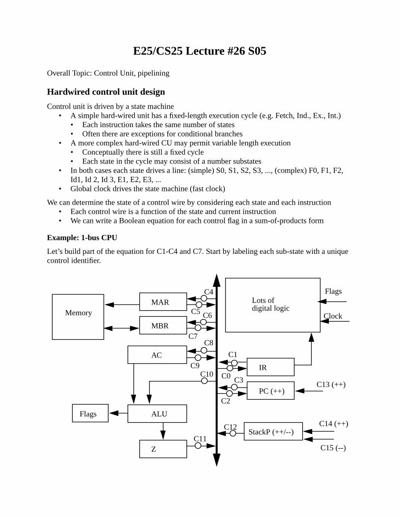
E25/CS25 Lecture #26 S05
Overall Topic: Control Unit, pipelining
Hardwired control unit design
Control unit is driven by a state machine• A simple hard-wired unit has a fixed-length execution cycle (e.g. Fetch, Ind., Ex., Int.)
• Each instruction takes the same number of states• Often there are exceptions for conditional branches
• A more complex hard-wired CU may permit variable length execution• Conceptually there is still a fixed cycle• Each state in the cycle may consist of a number substates
• In both cases each state drives a line: (simple) S0, S1, S2, S3, ..., (complex) F0, F1, F2, Id1, Id 2, Id 3, E1, E2, E3, ...
• Global clock drives the state machine (fast clock)
We can determine the state of a control wire by considering each state and each instruction• Each control wire is a function of the state and current instruction• We can write a Boolean equation for each control flag in a sum-of-products form
Example: 1-bus CPU
Let’s build part of the equation for C1-C4 and C7. Start by labeling each sub-state with a unique control identifier.
IR
PC (++)
MAR
MBR
AC
ALU
Z
Memory Clock
Flags
C1
C3
C2
C4
C5 C6
C7C8
C9C10
C11
C0
StackP (++/--)C12
Flags
C13 (++)
C14 (++)
C15 (--)
Lots of digital logic

Fetch cycle: • F0: PC -> MAR C3, C4• F1: Memory -> MBR; PC++ MemR, PC++• F2: MBR -> IR C7, C0
Indirect cycle:• ID0: IR[address] -> MAR C1, C4• ID1: Memory -> MBR MemR• ID2: MBR -> IR[address] C7, C0
Execute cycle (ALU op):• E0: IR[address] -> MAR C1, C4• E1: Memory -> MBR MemR• E2: MBR + AC -> Z C7, C10• E3: Z -> AC C11, C8
Now we can partially build the control flags C1-4, and C7• C1 = ID0 + E0 * (ALUop + ...) + E3 * (CALL + ...) + ...• C2 = E3 * (CALL + ...) + ...• C3 = F0 + E2 * (CALL + ...) + ...• C4 = F0 + ID0 + E0 * (ALUop + ...) + E1 * (CALL + ...) + ...• C7 = F2 + ID2 + E2 * (ALUop + ...) + ...
What we’re left with is a Boolean equation for each control flag. We can optimize these equations, and then build the circuit.
Hardwired v. Microprogrammed• Hardwired control is faster• Hardwired control is more complex• Hardwired control is more prone to errors in design (and more difficult to debug and fix)• Microprogrammed control is easier to design• Microprogrammed control is cheaper to implement• Microprogrammed control is easier to debug & fix• Microprogrammed control can be used to create a CPU with a modifiable instruction set• Hardwired control is faster (and that’s all that matters today)

Pipelining
Simple Pipelining• Develop an Instruction Fetch Unit [IFU]
• Fetch multiple instructions simultaneously• Do this in parallel with execution
IFU Outline• IFU has its own datapath to the bus (Harvard architecture)• IFU has its own MAR (usually different from the PC, but updated by the PC)• IFU has its own MBR, which is really part of a shift register• IFU is often connected to a read-only I-cache• IR loads instructions from the shift register• IFU tries to keep the queue full
State machine representation• Assume the shift register in the IFU has 6 positions• State machine has six positions• Load a new group of instructions when the shift register gets low
Special cases• Branching (writing to the PC) invalidates the instructions in the queue• IFU must be able to send NOP instructions to the IR to stall the CPU
• When the PC is written and it has to refill the shift register• When the IFU is unable to keep the queue full
Example: PIC Microcontroller• Program memory has a separate data path than data memory• Next instruction is always fetched on the previous cycle (incrementing PC)• A branch instruction takes two macrocycles [Branch | NOP] so that the PC can be reevalu-
ated and the correct next instruction fetched
Original Ultrasparcs didn’t have the capability to flush a pipeline, so the compiler had to insert NOP commands into the code after each conditional branch.
Modern Pipelining
Develop multiple stages in each of the macro-stages unit• Speed up the clock by making the data paths shorter• Use a multi-bus architecture• Use intermediate registers and/or scratch registers• Atomic operations become shorter parts of the cycle• Maintain the state of the computer in architectural registers
• Let’s you identify where interrupts occur & where to begin afterwards
F E
F E
F E
IFU Decoder OperandFetch
Execute OperandStore
OCUOpIssue
IFU Decoder OperandFetch
Execute OperandStore
OCUOpIssue

Typical modern pipeline stages• IFU: instruction fetch unit
• Keep the instructions coming• Decoder / Operand Fetch from Memory
• If a microcoded machine, map the macro-instruction to the appropriate set of micro-instructions
• If a RISC machine, this step lets control signals propagate or does not exist• Instruction Queue
• CISC machine: keep a set of microinstructions to be processed, dispatch one or more each clock cycle
• RISC machine: keep a set of instructions to be processed, dispatch one or more each clock cycle
• In both cases, this is where dependencies are determined• Decoder, Instruction Queue, and IFU communicate on branching issues
• Operand Fetch• Put the operands in the local ALU registers
• Execute• ALU path (may be pipelined itself)
• Operand Local Store• Move the operands from the ALU to local registers
• Operand Memory Store / Operation Commit Unit• Store operands to memory and/or architectural registers
The tricky part: you must be able to dump instructions (e.g. you are doing speculative execution) all the way through the queue, or you have to put in a lot of NOP statements.
Issues with a pipeline:• Not all instructions need all stages• Pipelining hopes that the stages can be executed in parallel
• One reason for separate caches for data & instructions• Conditional branch instructions void the pipeline
• A longer pipeline means this is more costly• Interrupts can really mess things up
• Either save the state of multiple instructions or lose work that’s already been done• Precise interrupts: interrupts happen between instruction completions
• The calculate operands stage may depend on an instruction that has not yet completed• Need to have logic that handles data-dependency
• A calculate operands stage may use a register that is in use for a previous instruction• Need to have logic that handles resource-conflicts• Handled by
• At each stage of the pipeline, data must move around• The data may actually move to a new location• The data may stay in the same place but change state information
• State information may be stored with the instruction and operands (K-6)• The amount of control logic required increases with more pipeline stages

E25/CS25 Lecture #27 S05
Overall Topic: Pipelining
Pipelining: Pipeline performance
What is the relative speedup for a given pipeline architecture?
First look at the minimum cycle time for a single pipeline stage
(1)
• is the maximum delay of the combinational logic for any single stage
• d is the time delay for a latch for signals to propagate from one side to the other
The total time Tk required to execute N instructions on a k-stage pipeline is given by:
(2)
• k = number of stages in the pipeline
The speedup factor is given by:
(3)
For large N, the speedup factor is . Because of setup time for latches (flip-flops), will always
be larger than , which means the speedup factor will always be less than k.
Long or short pipelines?
At first glance, a longer pipeline always seems to imply a faster execution rate• longer pipeline means simper stages and a faster clock• a faster clock means more instructions completed per second• basically doing more work in parallel
However, longer pipelines mean added complexity• In general for
• overhead in switching between pipeline states means an individual instruction takes longer• the control logic can actually become more complex than the processing logic
• the control logic may be the limiting factor on the maximum clock speed
Longer pipelines mean additional penalties for pipeline stalls or flushes• longer pipeline takes longer to startup after a flush• longer pipeline takes longer to execute code with data dependencies• longer pipeline contains more conditional branch statements
τ maxi τi( ) d+ τm d+= =
τm
T k k N 1–( )+[ ]τm=
Sk
T 1
T k------
Nτ1
k N 1–( )+[ ]τk-------------------------------------= =
τ1
τk----- τk
τ1
k-----
τk τm> k m>
Handling branching
Because flushing is so bad for pipelines, handling branches becomes a big deal in modern CPUs
There are two kinds of branches to deal with• Unconditional branches
• Put fast adders in the decode stage and calculate the target address• K-6 calculates the target address prior to decode completion
• Starts fetching instructions from the predicted target address immediately• No delay in the pipeline, especially given the instruction buffer after the decode stage
• Conditional branches• Do the same thing as with unconditional branches wrt calculating possible addresses
• K-6 calculates all possible addresses• Branch prediction unit selects the most likely address in parallel with the calculations
Mechanisms for handing branching• NOPs
• Put some NOP instructions into the pipeline after the conditional statement• When the result of the conditional is known, fetching continues from the right place
• Multiple streams• Have two instruction streams, and fetch both the next instruction and the branch target• Can cause contention delays for registers & memory access• Additional branch instructions may enter the pipelines, which makes it tricky
• Only really feasible for short pipelines• Prefetch branch target (general performance improvement)
• The target instruction is prefetched into an instruction buffer, but not put into the pipeline• May be some fraction of a line of cache, guaranteed to contain at least 1 instruction
• Saves fetch time on the next instruction whichever way it goes• Speculative Execution (general performance improvement)
• Target instruction is prefetched and put in the pipeline with special bits set• Instruction may make it through the pipeline but never be “committed”• Usually used along with branch prediction since only one branch is generally prefetched
• Loop buffer (general improvement mechanism)• A small high-speed buffer that contains the n most recently fetched instructions
• Loop buffer may contain some of the instructions ahead of the current fetch address, reducing access time for those instructions
• If a branch occurs to a location slightly ahead of the branch instruction, this instruction will be in the loop buffer (useful for IF-THEN-ELSE)
• The strategy is well-suited to loops• Branch target cache (general improvement mechanism)
• When a branch instruction hits the decoder, figure out where the branch goes to• Load instructions from that target address into the branch target cache• Pull speculative instructions from the target cache if the branch is predicted to happen
• Only works, of course, if the branch was the last one taken• On a loop, the branch target cache allows instructions to be fetched without delay• K6 holds 16 bytes for each of the last 16 branches (conditional or unconditional)

• Return address cache (general improvement mechanism)• When a CALL executed, save the return address to the stack and the return address cache• When a return is executed, pull the most recent return address from the return address
cache and speculatively use it to start fetching instructions• Compare to the true value off the stack at some later point• K-6 does this with a 16-entry return address stack
• Branch prediction (general improvement mechanism)• You try to guess which way things are going to go (usually based on a fixed rule or his-
tory), and then prefetch that instruction.• Dump things only if you guessed wrong.
The science of branch prediction
Up to 10% of a typical application consists of unconditional branches
Up to 10-20% of a typical application consists of conditional branches
• Predict never taken• minimizes extra page accesses & loads• pages are how the operating system manages virtual memory, not all pages are in memory
at all times, so sometimes a page must be read from the disk
• Predict always taken• branches are taken > 50% of the time, so if the cost is the same, this is a good strategy• It means you need to pre-calculate the branch target addresses very quickly• Loops are an example of a branch taken most of the time
• Predict by opcode• some branch types tend to be taken, while others are not• can get success rates > 75% with this strategy• Example: branch if not zero is usually the end of a for loop (so take it)
• Always take conditional branches that go back, never take branches forward [BTFN]• backwards branches are generally loops• forwards branches are often error conditions [if (fp != NULL) {execute program}]
• Taken/Not taken switch• Store a bit in cache with the instruction giving the last history of the instruction• Follow history since it tends to repeat itself• Two bits (4 history states) works better since it can specify a more complex strategy• We can write a state machine to represent this (only change after two errors)
• Branch history table• Small cache memory• Save three fields: the address of the branch instruction, the history, and the target address
Take itTake it Don’t take Don’t take
TakenTaken Taken Taken
Not Taken Not Taken Not Taken Not Taken

or target instruction (history could be used as a state machine)• Since K-6 does address calculations on the fly, it only stores history information• You can use this in tandem with a branch target cache
• Branch key• Have a key which is N bits long, representing how the last N branches have gone• Save the keys for the most recent instructions• Look for a match with recent keys and do the same thing as before
• Have the compiler help out• Some instructions let the compiler put a guess as to where the branch will go• Compiler can put in NOP statements• US II does some of this, IA-64 architecture is explicit about it

E25/CS25 Lecture #28 S05
Overall Topic: Branch Prediction
Branch Prediction on the K-6
A lot of the work for branching is executed in the decoder stage where the CISC instructions are converted into RISC instructions
• Branch decoder unit pre-calculates target addresses for branches• Predictor simultaneously decides which direction to take
• Based on an 8192-entry Branch History Table [BHT]• Method is a “two-level adaptive branch direction prediction algorithm”
• Predictor selects one of the calculated addresses and sends it to either the L1 cache or the Branch Target Cache (which holds instructions from up to 16 of the most recent branches)
Two-level adaptive prediction algorithms• Branch history table contains k-bits for each entry indicating what happened in the past
• Think of the k-bits as a string that tells you a pattern (6-12 bits, for example)• You get 0.5% increase in accuracy for each 2 additioanl bits from 6-12• 0 = not take; 1 = taken (or whatever convention you choose)
• Branch history table entry is an index into a global pattern table (lookup table)• Global pattern table has 2k entries.• Each string of k-bits has an entry in the table• Prediction is a function purely of the global pattern table bits S1-Sn
• When the branch is resolved, both the BHT and the global pattern table are updated• Result is shifted into the low bit of the BHT entry• Global pattern table is updated according to a function
• Think of the bits S1-Sn as the state of a state machine• The prediction is a function of the state only• When a prediction is made, the state is updated according to the correct result• Can experiment with the kind of state machines you use• A simple state machine has 2 states (1 bit), a better solution is 4 states (2 bits)
• Benefits of a two-level adaptive algorithm• Learns typical behavior of a program through the global pattern table• Each branch still gets to express its individuality in the patterns• What the system is doing is dynamically learning statistics for branching patterns
This algorithm achieved 97% accuracy on 9 of 10 SPEC benchmarks [Yeh & Patt, 1991]• 10th one (Nasa7) didn’t test conditional branches well in a reasonable amount of time
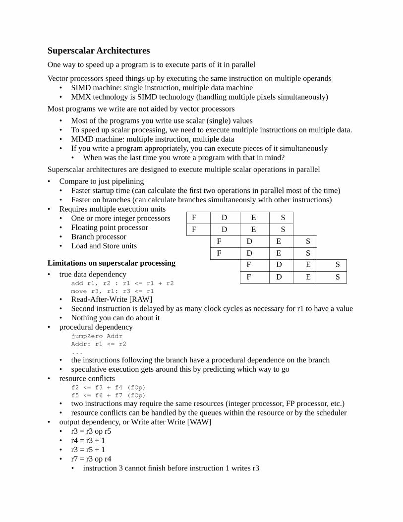
Superscalar Architectures
One way to speed up a program is to execute parts of it in parallel
Vector processors speed things up by executing the same instruction on multiple operands• SIMD machine: single instruction, multiple data machine• MMX technology is SIMD technology (handling multiple pixels simultaneously)
Most programs we write are not aided by vector processors
• Most of the programs you write use scalar (single) values• To speed up scalar processing, we need to execute multiple instructions on multiple data.• MIMD machine: multiple instruction, multiple data• If you write a program appropriately, you can execute pieces of it simultaneously
• When was the last time you wrote a program with that in mind?
Superscalar architectures are designed to execute multiple scalar operations in parallel
• Compare to just pipelining• Faster startup time (can calculate the first two operations in parallel most of the time)• Faster on branches (can calculate branches simultaneously with other instructions)
• Requires multiple execution units• One or more integer processors• Floating point processor• Branch processor• Load and Store units
Limitations on superscalar processing• true data dependency
add r1, r2 : r1 <= r1 + r2move r3, r1: r3 <= r1
• Read-After-Write [RAW]• Second instruction is delayed by as many clock cycles as necessary for r1 to have a value• Nothing you can do about it
• procedural dependencyjumpZero AddrAddr: r1 <= r2...
• the instructions following the branch have a procedural dependence on the branch• speculative execution gets around this by predicting which way to go
• resource conflictsf2 <= f3 + f4 (fOp)f5 <= f6 + f7 (fOp)
• two instructions may require the same resources (integer processor, FP processor, etc.)• resource conflicts can be handled by the queues within the resource or by the scheduler
• output dependency, or Write after Write [WAW]• r3 = r3 op r5• r4 = r3 + 1• r3 = r5 + 1• r7 = r3 op r4
• instruction 3 cannot finish before instruction 1 writes r3
F D E S
F D E S
F D E S
F D E S
F D E S
F D E S
• Write-After-Read [WAR]• Same as above, but instruction 3 cannot finish before instruction 2 reads its value• Third instruction destroys a value the second uses• This is also called antidependency
What if: we could rename physical registers• Rename r3 wrt the first two instructions as r3a• Could execute the first two instructions and the last two instructions in parallel• Concept is register renaming• Modern processors all do register renaming to get around WAW and WAR conflicts

E25/CS25 Lecture #29 S05
Overall Topic: Superscalar processing
Superscalar Architectures: Instruction issue policy
With multiple functional units we need to issue multiple instructions per cycle
Do they start in order, and do they finish in order?
In order issue, in order completion
Baseline policy
Assume
• Two fetch/decode stages• Three different functional units• Two writeback pipelines
Example (6 instructions with constraints):
• I1 requires 2 cycles to execute• I3 and I4 use the same functional unit• I5 depends on the value produced by I4• I5 and I6 use the same functional unit (but a different one than I3/I4)
Machine architecture constraints
• Instructions are fetched 2 at a time• The next pair must wait until the execution phase is cleared (in-order completion)• Instruction issuing stalls when there is a conflict of functional units
Decode Execute Writeback (2 pipelines) Cycle
I1 I2 1I3 I4 I1 I2 2I3 I4 I1 I2 3
I4 I3 I1 I2 4I5 I6 I4 I3 5
I6 I5 I4 6I6 I5 7
I6 8
• Elapsed time is 8 cycles• Note: I3 can’t be issued in time-step 3 because writeback stage would be full
In order issue with out-of-order completion• Improves performance of multiple cycle instructions since it doesn’t hold up the pipeline• Works well when there is no data dependence• Used on some RISC machines• Any number of instructions may be in the execution queue, limited by the functional units
Instruction issuing is only stalled when there is
• data dependency• resource conflict

• output dependency (a newer instruction must wait if its output would be overwritten by an older instruction
Look at the same I1-I6 example with out of order completion
• Don’t have to wait to send things to the execution state because writeback now has room
Decode Execute Writeback (2 pipelines) Cycle
I1 I2 1I3 I4 I1 I2 2
I4 I1 I3 I2 3I5 I6 I4 I1 I3 4
I6 I5 I4 5I6 I5 6
I6 7
out-of-order issue with out-of-order completion
Decouple the fetch/decode stage with the execution stage
Allow the processor to look ahead in the instruction queue and get beyond dependencies
Use an Instruction Window to hold instructions, and the window can be large & always full
• Instruction window is a buffer of fetched and decoded instructions• As long as the instruction window is not full, continue to fetch and decode instructions• Any instruction in the instruction window can be executed so long as:
• a) there is a functional unit available for it to execute on, and• b) no conflicts or dependencies block this instruction (you have antidependency now)
Look at the previous example with out of order completion and a queue for out-of-order issueDecode Execute Writeback (2 pipelines) Cycle
I1 I2 1I3 I4 I1 I2 2I5 I6 I1 I3 I2 3
I6 I4 I1 I3 4I5 I4 I6 5
I5 6
Out of order completion is tough because it is difficult to define the state of the computer
The big problem with out-of-order completion is that it is difficult to define when an interrupt, trap, or fault actually occurred. It can also be more difficult to manage dependencies.
Out of order issue with in-order completion• In-order completion allows for precise interrupts, traps, and faults
• Makes it easier to keep track of the architectural registers and “state” of the CPU• IFU holds instructions to be executed
• Can search for instructions whose operands are available• Instruction buffer holds instructions to be “committed”
• Instructions are committed in-order, so they wait in a queue until it’s their turn• Multiple instructions can be committed simultaneously

• Good way of balancing the need for precise interrupts with balanced usage of resources• You need a lot of registers because there are many temporary values waiting to be committed.
Look at the example with in-order completion and a queue for out-of-order issue
Decode Execute Writeback (2 pipelines) Cycle
I1 I2 1I3 I4 I1 I2 2I5 I6 I1 I3 3
I6 I4 I1 I2 4I5 I3 I4 5
I5 I6 6
Register renaming• Many resource conflicts have to do with a particular compiler’s register use schemes
• Different compilers/languages/architectures have traditional usages for each register• output dependencies• antidependencies• Both are caused by not being able to read/write to a register in use by another instruction
• Optimizing compilers try to make maximum use of registers, which maximizes dependencies
A solution is register renaming
• dynamic allocation of registers by the processor (not the compiler)• Have lots of “secret” registers that can be used as scratch registers• The “architectural” registers are then updated each time an instruction is committed
Scoreboards
Attach an N bit counter to each register to see how many times it is a source for current ops• Registers can be read by multiple instructions• No instruction can write to a source register until it has been read by pending ops
Attach a 1 bit counter to each register to see how many times it is being written by current ops• No instruction can read a register until it has been written by pending ops
Use a counter to keep track of functional unit usage
Rules1. If any operand of an op is being written, do not issue (RAW)2. If any result register is being read, do not issue (WAR)3. If the result register is being written, do not issue (WAW)
Once you identify WAR/WAW dependencies, use scratch registers

E25/CS25 Lecture #30 S05
Overall Topic: Real CPU Designs
Real Design #1: K6 3D
K6 is• CISC on RISC: CISC instructions are decoded to a set of RISC instructions• Fairly heavily pipelined (6 major stages, 6-10 substages in the execution pipeline)• Superscalar (up to 6 micro-instructions issued each clock cycle, up to 4 retired)• Allows speculative execution with branch prediction• Allows out-of-order execution• Uses in-order completion to facilitate precise interrupts, traps, and faults
I-Cache• 64KB 2-way associative cache with 64 bytes/line• MESI cache coherency protocol
• Instruction cache only has two states: valid, invalid since they are read-only• 64 bytes are filled 1/2 at a time
• If a miss occurs, the half of the line with the desired location is filled• The other half-line is tagged, but marked invalid• If the other half-line is needed, it is loaded from memory and the tags stay the same
• I-cache is read-only, and predecodes each byte as it comes in• Predecoder identifies where the beginning of each instruction is• This is a complex assignment in the x86 architecture
Instruction Buffer• Fetches 16 bytes per cycle from the I-cache or the Branch Target Cache
• Branch Target Cache helps out with branch prediction so target can be prefetched• BTC holds the first 16 instruction bytes of up to 16 previous branches
• This data is not necessarily in the I-cache
Decoder• Up to two x86 instructions are decoded per cycle
• Some are decoded by the “short” decoder (fast)• There are two short decoders
• Some need the “long” decoder (only 1)• Some have RiscOP sequences stored in a control ROM (only 1)
• Decoder converts the x86 instruction into the K6 RISC ops• RISC ops are sent to the scheduler in OpQuads, four at a time (NoOps pad the OpQuad)
Scheduler• Scheduler holds 24 Ops, in 6 rows of four
• Each scheduler OpQuad is 578+ bits of information• All the information about an Op’s state is held in the scheduler• Each scheduler entry holds the result of that operation (implicit register renaming)
• The ops in row 5 are the oldest

• Ops move through in OpQuads and are retired as OpQuads (up to 4 at a time)• When the bottom row is committed or retired, all of the rows move down• Most Ops in the scheduler can be executed at any time
• Older ops (lower down) are more likely to be executed• The operands for the Op must be available (data dependency)• An op is only executed if an execution unit is available for it (resource dependency)
• Branch Ops aren’t executed until they reach a specific row (3)• No use having BRU logic in higher rows since the conditions probably won’t be set
• Load and Store Ops are likely to be started early since they can take multiple cycles• Scheduler uses scan-chains to:
• Select ops to issue• Find the oldest un-issued instruction for each functional unit
• Discover where operands are• Start at the youngest instruction that is older than the current one• Last/default value is the architectural register• The first place an operand is found is its source
Execution Pipeline• Issue selection phase
• Scan chain from oldest to youngest to discover un-issued ops for each execution unit• Operand Information Broadcast Phase
• Scan chain from to discover where the operands are going to come from• Architectural registers: oldest case, ops already committed• Result registers in ops in the scheduler: use the youngest older than the op• Execution pipeline bus: the result will have just been calculated (bypass mode)
• The scan chain doesn’t actually include the results buses; that decision is made later• Operand Selection Phase
• Make the selection of where the operand is to come from• This is where the results bus is considered
• Operand Transfer Phase• Transfer the operand to the execution pipeline• Simultaneously figure out if the operand is valid or not
• The operand may need to come from an op that hasn’t executed yet• Only send the op to Stage 1 of the Execution queue if the operands are valid• Otherwise, “Bump” the instruction and label it as un-issued
• It can be re-issued in the next clock cycle• Execution Stage
• Send the results through the ALU, Load Unit, or Store Unit• Result Transfer Phase
• Send the results back to the result register in the op scheduler entry or to a queue
Overall comments:• Ops are selected for issue based only on the functional unit they require• Operand location and validity is determined in a later stage• This mechanism means that there is no peeking at earlier instructions
• The 24-op instruction is probably sufficient for this case

Commit Unit• When all four ops in the bottom OpQuad have been issued and executed, and there are no
traps, faults, or interrupts, then commit the bottom row of the scheduler and write the results to the architectural registers
• Move the rest of the scheduler OpQuads down a row
Faults, Traps and Missed Branches
The BRU and the OCU are in charge of handling fualts, traps, interrupts, and missed branches
BRU• If the BRU finds a missed branch
• Flush the upper half• Allow older ops in the scheduler to commit• Flush the lower half• A new OpQuad can be loaded into the scheduler simuntaneously with the flushing
OCU• If the OCU finds a trap, fault, or interrupt
• Flush the upper half• Commit older ops in the scheduler• Save the architectural state• Flush the lower half
K-6 Superscalar characteristics• It can issue up to 6 RISC86 ops per cycle using out-of-order issue
• Corresponds to 1 or 2 IA-32 ops• It can reture up to 4 RISC86 ops per cycle (bottom row of scheduler) in-order• Register renaming is accomplished implicitly
• 24 architectural registers (8 correspond to IA-32 instruction set)• 24 scratch registers in the scheduler (1 for each op result)• Order of scan-chains determines which registers are used for a given Op
• Dependencies are handled by bumping instructions out of the execution queue

E25/CS25 Lecture #31 S05
Overall Topic: Real CPU Designs
Real Design #2: AMD K-7 (enhanced architecture)
Conceptually, the K-7 is not that different from the K-7• Superscalar• Speculative execution with branch prediction• Heavily pipelined• Out of order issues / in-order completion• Split D/I cache with predecoding in the instruction cache
In its implementation, it simply has more and does more than the K-6
The main cache is larger• 64K each of data and instruction cache• The data cache can permit concurrent access by two 64-bit loads or stores• the branch prediction table has only 2048, down from 8192 (too big?), still 2-way SA
The decoding is executed with three pipelines instead of two• Each decoder can handle any instruction (they are called “full x86 instruction decoders”)• Instead of multiple RISCOps, the decoders generate fixed-length MacroOPs
• It looks like the MacroOPs are less RISC-like than on the K-6
The scheduler (now the Instruction Control Unit [ICU]) can hold 72 MacroOPs• This is more than six times the K-6, which could hold at most 12 short IA-32 instructions• Up to 3 MacroOPs per cycle are sent to the ICU
The execution pipelines have more stages• 10-stage integer pipeline• 15-stage floating point pipeline
There are more execution units• 3 address-calculation functional units (used to be handled in the Load/Store units)• 3 complete integer functional units• 3 floating point functional units (different functionality)
• One handles loads and stores (FSTORE pipeline)• One handles FP adds and related MMX commands (FADD pipeline)• One handles FP multiplies and related MMX commands (FMUL pipeline)
The scheduler doesn’t actually send off the instructions any more• The integer/addres calculation units have their own 18-entry out-of-order issue queue• The floating point/Multimedia units have their own 36-entry out-of-order issue queue• Note that this lets the functional units issue operations based on operand validity
Overall, it does more than the K-6 at a faster clock speed, while still holding onto the same basic concepts of CISC on RISC with superscalar speculative processing.

Real Design #3: Pentium IV (superpipelined superscalar CISC on RISC)
The goals of the PIV appear to be maximizing clock speed and optimizing streaming applications.
Decoding pipeline• Instructions are fetched sequentially from the L2 cache in 64 byte lines• The cache line is scanned for instruction boundaries• The decoder translates the IA-32 instructions into 1-4 118-bit RISC ops• IA-32 instructions that require more RISC ops get stored as a placeholder (decoded later)• The RISC-ops end up in the trace cache (L1 I-cache)• Branches get predicted statically (FNBT) at this stage• A branch target buffer [BTB] assists the branch fetching
L1 pipeline• The L1 cache includes its own BTB
• 512 lines, organized as a 4-way associative cache with addresses as the tag• The RISC pipeline includes its own branch prediction mechanism using 4 history bits• Trace cache next instruction pointer (2): identifies next instruction trace
• a trace is a program ordered group of three RISC-op instructions• Trace cache fetch (2): fetches & assembles the next trace
• Long IA-32 instructions get sequenced from the RISC-op microcode• Drive (1): moves the trace to the execution logic
• This is basically moving instructions from the L1 cache into the “CPU”
Execution Logic• Allocate (1): allocate resources for execution
• Allocates an entry in the re-order buffer [ROB], a 126 entry instruction buffer• Allocates a temporary register for the instruction (128 available)• If a resource is unavailable, it stalls this stage of the pipeline• The goal is to keep the ROB full
• Register Renaming (2): handles register renaming• Maps the temporary register allocated for the instruction to an architectural register• Handle WAW and WAR dependencies
• Micro-op Queuing (1): places the instruction in one of the two micro-op queues• One queue holds memory operations, the other non-memory operations• The queues individually maintain a FIFO ordering• There is no synchronization between queues, so instructions will be out of order
• Micro-op Scheduling and Dispatching (5): sends micro-ops to the execution units• The scheduler can grab multiple instructions out of a queue• It grabs them in FIFO order for a given execution unit• It can issue up to six RISC-ops in a single cycle• Only ops with valid operands get scheduled
• Register File (2): grabs the operands and submits them to the execution units• May grab operands from the L1 Data cache, situated next to the execution units
• Execution (1): executes the operation• Flags (1): sets the appropriate flags• Branch Check (1): tests pending branches• Drive (1): write the results of the operation / write branching results to the BTB

Real Design #4: PowerPC 601
The PowerPC 601--the first desktop microprocessor of that architecture--is an example of a sim-ple superscalar pipelined computer.
Major characteristics:• Unified cache• Cache arbitration unit that orders access to the unified cache• Static branch prediction• No register renaming (implicit or explicit)• Three execution units: branch unit, integer unit (load/store), floating point unit
Dispatch unit:• Upper half--4 instructions--is a simple instruction buffer • Lower half--4 instructions--available for execution• Integer instructions are issued in-order• Branch and floating point intructions are issued out-of-order
Execution units• Branch unit: two-stage pipeline, PowerPC has 8 condition registers
• Intelligent compilers can ensure that conditions codes are preset so there is no delay• Integer unit
• 4-stage pipeline for integer instructions• 5-stage pipeilne for load/store
• Floating point unit• 6-stage pipeline w/two execute stages
Branch handling• Fetch unit continues to fetch sequentially until a branch enters the low half of the queue• Branch unit determines if the branch direction is known
• If the direction is known, execution proceeds • If the direction is unknown, prediction is FNBT• Target addresses are computed when a branch hits the low half of the queue
• Instructions past a prediction are executed conditionally • If the guess was correct the conditional instructions are committed• If the guess was incorrect the conditional instructions are flushed
• Condition codes are usually known in advance• Large number of condition code registers, compilers can pre-compute conditions• Integer instructions are executed in order, branches out of order
• Even on mis-predicts, the recover is fast• Branch unit only takes 2 cycles to execute• Fetch unit can get 8 instructions from cache in a single cycle• Most missed branches result in a 2 cycle pipeline delay
Newer members of the PowerPC family have 6 execution units, split caches, and do prediction

E25/CS25 Lecture #32 S05
Overall Topic: Hyperthreading and I-A 64
Real Design #5: PIV with Hyperthreading
Hyperthreading is a real modification to the computer organization and design
The most basic problem of supeerscalar architectures is that dependencies make it inefficient• Adding execution unit smeans more instructions that can execute• If more instructions are in play, tha tmeans more dependencies• Getting around dependencies requires a larger instruction window/longer horizon
Hyperthreading takes a different approach to solving the superscalar limitations
Make your CPU look like a dual-core processor• Provide two, completely independent architectural states (register sets)• One integrated cache structure (L1-I and L1-D / L2 / L3)• Fetch instructions alternately for two threads
• Keep instructions in groups• Execution engine does not differentiate between the two threads (out-of-order execution)• Reorder engine puts the instructions back into groups based on their thread• Thread groups are retired in alternate order (if two threads are running)
Goal of hyperthreading is to make maximal use of the resources that exist• Threads are generally independent entities (no dependencies)
New Design: IA-64 Explicit Parallel Instruction Computing
The problem: processor designers have more transistors than they know what to do with.
Options:• Increase cache size
• Marginal benefits in the hit rate• Main memories are getting faster and higher bandwidth
• Increase pipeline length• Requires increased effort at branch prediction• Increases likelihood of a mispredicted branch• Increases the penalty for a mispredicted branch• Marginal benefits beyond current capabilities
• Increase the degree of superscalar capability• Requires increased effort at branch prediction• Requires more complex logic for control• Requires more invisible registers to avoid WAW and WAR dependencies• Marginal benefits beyond current capabilities
• Increase SIMD capability• Requires hand-coding in assembly • Requires more sophisticated software tools & compilers• Not everything is SIMD

One possible solution: Explicitly Parallel Instruction Computing [EPIC]• Pass the burden of parallelizing code to the compiler• The compiler has orders of magnitude more time & computing power• The compiler can look at a program as a whole and search for parallelizable code
With EPIC, the degree of parallelism/superscalar capability is not limited by the complexity of the control logic, but by the number of execution units (and these are growing exponentially)
• Can still use the SIMD option as well for special case computing
IA-64 Main Concepts
Large number of registers that are visible to the compiler• The compiler has to have the resources to create the parallelism• Large = 128 integer + 128 floating point + lots of special-purpose registers
Bundled instructions (compiler responsibilities)• Instructions come in a 128 bit bundle of three 41-bit instructions plus a 5-bit template• The template indicates parallelizability and functional unit for each instruction• The template can explicitly mark data dependencies
Predicate registers• Normal instructions are conditional based on control instructions (branches)• EPIC makes all instructions conditional, based on a predicate register
• The instruction is only committed if its predicate register is true • 64 predicate registers give the compiler flexibility• Both sides of an if statement can be executed in parallel, meaning no pipeline flushing
Specifics of the IA-64 Architecture
Speculative execution of multiple paths• Typical approach to branching is to guess one path and speculatively execute it
• If you get it wrong, go down the other path after flushing the pipeline• IA-64 uses predicate registers to speculatively execute both paths in parallel
• Since every instruction is predicated, there is no pipeline flushing• Tradeoff of space (execution units) for time
Example: conditional branching on a Pentium
cmp a, 0 ; compare a with 0 [ if(a && b) then ]je L1 ; branch to L1 if a = 0cmp b, 0 ; compare b with 0je L1 ; branch to L1 if b = 0add j, 1 ; add 1 to j [ j = j + 1; ]jmp L3 ; unconditional branch to L3
L1: cmp c, 0 ; compare c with 0 [ else if(c) then ]je L2 ; branch to L2 if c = 0add k, 1 ; add 1 to k [ k = k + 1; ]jmp L3 ; unconditional branch to L3
L2: sub k, 1 ; add -1 to k [ else k = k-1; ]L3: add i, 1 ; add 1 to i [ i = i + 1; ]
Same example on an Itanium:

cmp.eq p1, p2 = 0, a ; compare a to 0, set p1=true, p2=false if true(p2) cmp.eq p1, p3 = 0, b ; compare b to 0, set p1=true, p3=false if true(p3) add j = 1, j ; j = 1 + j, commit if p3 is true(p1) comp.ne p4, p5 = 0, c ; compare c to 0, set p4=true, p5=false if false(p4) add k = 1, k ; k = 1 + k, commit if p4 is true (c != 0)(p5) add k = -1, k ; k = -1 + k, commit if p5 is true (c == 0)
add i = 1, i ; i = 1 + i, not predicated
Note that the Itanium code takes 7 instructions to execute, with potentially 3 of them being dis-carded after execution, but no pipeline flush. If the Pentium does perfect prediction, it executes at least 6 instructions, and has to do fast address calculation to keep the pipeline full.
Speculative Loads (control speculation)• Compilers can move loads to well before they are/are not needed• Compiler inserts a CHECK statement just before the value is needed• If the value is there, CHECK is a NOP• If the value is not there or the LOAD caused an exception, the CPU handles it• Loads may be done off the critical path and check statements inserted• Example:
if(a < b) LOAD Celse LOAD D
LOAD CLOAD D;; do some other stuffif(a < b) CHECK Celse CHECK D
• The check statements just check for exceptions. If one occurred, then the handler is called, otherwise processing continues.
• The compiler may also move loads before subsequent stores (data speculation)• The compiler inserts a check statement where the load would have occurred• The processor dynamically checks to see if the load was successful (if another instruc-
tion had written to that location after the advanced load);; example of typical code, [r8] may not be the same as [r4]st8 [r4] = r12 // cycle 0ld8 r6 = [r8] // cycle 0add r = r6, r7 // cycle 2 (2 cycle delay for the load)st8 [r18] = r5 // cycle 3 (data dependency)
;; example of data speculationld8.a r6 = [r8] // cycle -2 or earlier;; other code herest8 [r4] = r12 // cycle 0ld8.c r6 = [r8] // cycle 0 (check load)add r5 = r6, r7 // cycle 0 (value is already there)st8 [r18] = r5 // cycle 1
Register stack• Dynamic renaming of registers to handle subroutines (lots more than 128 registers)
• Base pointer to a set of registers• The base pointer gets reset on a return call

• The processor dynamically handles spilling and refilling registers for subroutine calls• If it overflows the register stack, then some are dumped to memory• Upon return, if some are in memory it recalls them by stalling• The processor can dynamically decide when to spill and refill to avoid stalling
Branching• When branching does happen, branch registers are used to hold target addresses
• Makes address calculations faster• Loop-closing branches provide information that allows for perfect prediction
Loop scheduling (software pipelining)• The compiler can unroll loops to achieve faster execution of loops in parallel
• Have to handle register renaming appropriately• Loop iterations can’t have dependencies on each other
• Automatic register renaming for a set of registers• If a loop used r32 in iteration 1, then it uses r33 on iteration 2
• Rotating predicate registers• Loop terminating instructions that permit perfect prediction of control• Loop pipelining has three phases
• prolog: each cycle a new loop gets started until N iterations are going at once• kernel: N iterations keep the pipeline full• epilog: no new iterations start, the pipeline clears out
• There are specific registers to be used as loop counters and epilog counters• There is a specific branch instruction for loops• The loop branch decrements the counters and executes the register rotation scheme
Floating point architecture• single, double, double-extended (80 bit) supported• 96 registers can be used for register rotation and loop support• fused multiply and add instructions (all in one)• parallel instructions that operate on two 32-bit FP values (SIMD)
MMX style instructions• eight 8-bit values, four 16-bit values, two 32-bit values in a single register
Cache• Itanium 2 has a 3MB L3 cache, 256K L2 cache, and 16K data and 16K instruction L1• All on chip (L3 in the package)
Other registers
• 8 registers used for branch address calculations• 8 registers for use by the OS kernel to communicate to applications• registers for managing the register stack configuration• Status registers for user applications and floating point unit• Loop count register• Epilog count register• Compare and exchange value [CCV] register (useful for parallel processing)• Many, many others...

E25/CS25 Lecture #33 S05
Overall Topic: OS Support
Operating System Level
Operating system is in charge of starting and terminating programs, managing I/O transactions and generally making sure each device is talking to every other device.
• Programs get swapped in and out of memory• They don’t go to the same place each time
• At the very least, all addresses in a program are relative to a base pointer• What if you want virtual memory (logical memory > physical memory)?• What support is helpful at the architecture level?
Modern OSs are running multiple programs, or multiple threads of a single program
• One method of reducing data dependencies within a processor is to run multiple threads• The threads are guaranteed to be data independent• From the point of view of the OS, there need to be two or more logical processors• How can the architecture support the appearance of two or more logical processors?
• Hyperthreading (architecture looks like 2 processors)• Dual-core processors (architecture is 2 processors)• Context swapping and virtual memory (support the OS maintaining the illusion)
Addressing
Given all of this swapping in and out is, how does a program know where it is in memory?• addresses of data items (load and write)• addresses of instructions (jump statements)• These addresses could change, not just each time a program is loaded, but when a program
is swapped in and out of memory, and even during program execution when memory is compacted.
How do we manage memory in a way that solves these problems?
The two major approaches to memory management are paging and segmentation• Paging is a method of memory management that is invisible to the application
• Generally used to implement virtual memory• Segmentation is a method of memory management that is visible to the application
• Visible means visible at a very low level• Generally used to implement memory protection
Both are based on the idea of logical addresses, linear addresses, and physical addresses• Logical address is relative to the program’s beginning (relative to a segment pointer)
• Program pretends it is the only program in memory and starts at location zero• Linear address is relative to the effective address space (limited by the #bits in the address)• Physical address is an actual location in main memory (limited by $ and space)• CPU/OS maintains a base linear address for each program, which is how it discovers the
linear address from the logical address within a program.

Paging
Page - small fixed-size chunk of a program which maps to a frame, or page frame in memory• page: the chunk of data/program• frame: a page-sized chunk of physical memory (equivalent of a line in a cache)• The pages of a program do not need to be consecutive• OS maintains a list of free pages• OS loads a new program into the free pages, wherever they are
• If there are no free pages, it has to dump some of the existing pages to disk• OS has to keep track of which pages a program occupies
With paging, compiler can write addresses in programs to be page relative• A program knows how many pages it needs (approximately)• The program can write addresses as page + offset• Then the processor just needs a method of looking up where the pages are located
Page Tables• The page table holds the frame location for each page of a process• The location of a page in the table is calculated from the high bits of the linear address
• Conceptually, the linear address / page size• Physical address is computed from the page table and the low bits of the linear address
• Relative address is the linear address modulo the page size• CPU architecture needs to be able to use the page table to produce a physical address
• 8 pages of virtual memory (23), but only 4 pages can fit in main memory
• Each page is 32 bytes (25), for a total of 128 bytes (27) of physical memory
What address do the following map virtual addresses map to?• 5 -> 0x05 -> top three bits are 000 -> virtual page 0 -> on disk• 33 -> 0x21 -> top three bits are 001 -> virtual page 1 -> page frame 1 -> 001/0 0001• 70 -> 0x46 -> top three bits are 010 -> virtual page 2 -> page frame 0 -> 000/0 0110• 223 -> 0xDF -> top three bits are 110 -> virtual page 6 -> page frame 2 -> 010/1 1111
Table 1: Example state of a paged memory system
Page frame (physical)
Page frame address(physical)
Page(virtual)
Location(virtual)
0 0x00 0 disk
1 0x20 1 page frame 1
2 0x40 2 page frame 0
3 0x60 3 disk
4 disk
5 page frame 3
6 page frame 2
7 disk

Caching and Paging
Do you use linear or physical addresses in L1 and L2 cache?• Physical addresses are good for L2 cache because they facilitate snooping and cache
coherence protocols (a piece of data has only one physical address)• Physical addresses are not so good for L1 because they depend upon the page table
• You don’t want to be storing much of the page table in your L1 cache• You don’t want to risk paging from disk just to do memory address translation
Nevertheless, that’s what cache’s do, but certain things make it faster• If you can calculate the set/line independent of the page table it’s faster
• Low bits tell what line to search for a tag, calculate the tag simultaneously• Page size has to be larger than the (cache size / set-associativity)
• Need to have access to the page table in order to generate tags for comparison• Special caches store pieces of the page table to avoid holding them in L1• Special adders & lookup logic calculates physical addresses from linear addresses
Paging requires hardware support for reasonable speed.
Virtual Memory
Virtual memory is easy with paging: not all of the pages of a process need to be in memory
A page fault interrupt is generated when the page is not in memory• page fault interrupt loads the needed page(s)• This is termed “demand paging”• page faults are invisible to the user or application
If memory is full, it means you have to dump a page• Least recently used
• pathological case is a large loop• Circular buffer (FIFO)
• Can experience the same pathological case• OS has to use fairly complex algorithms to avoid thrashing (loading pages continuously)
• The OS looks at recent usage patterns and tries to avoid dumping pages it may need in the near future
Write-back issues are similar to that of cache• When a page gets replaced it needs to be written back to disk if it has changed• Most OS’s use a write-back policy (only write-back when the page needs to be replaced• Could experience the same problems as a cache write-back policy when multiple
machines are using a shared virtual memory
E25/CS25 Lecture #34 S05
Overall Topic: OS Support
Operating System Level: Page Table Structure
Hardware implementation• Special purpose register holds the start of the page table in main memory• Page number of current address indexes into the page table• Table holds the corresponding frame number for that page• Frame number and offset portion of the address create the physical address
Problems
• Page tables can be huge• Parts of the page table are often stored on disk,; only parts of the page table are stored in
memory at any given time.• Thus, a page table access may involve a disk access (really slow)
• Each memory access involves two memory accesses (doubles memory access time)
One solution is to use a translation lookaside buffer (page table cache)
• Page table information on the most recently used pages are in the TLB• CPU consults TLB to see if the section of the page table is present• If not, it’s loaded from memory (if it’s not in memory, it’s loaded from disk)• CPU generates the real address and consults the cache to see if the data is there• If the cache misses, it’s loaded from memory (if it’s not in memory, it’s loaded from disk
and the page table entry is updated)
Implementing paging and segmentation
Swapped segments (no paging)• Bring segments in and out of memory as needed• Fill available “holes” in memory with segments that will fit• Need to compact and combine holes dynamically• It is up to the OS to ensure that segments do not overlap (conceptually they can)
Segmentation with paging• Each segment has its own page table• Pages are brought in and out as needed• Conceptually, the programmer can create many segments the size of the linear address
space without worrying about overwriting other segments
You can have both paging and segmentation
• Unsegmented, unpaged memory• base address of the program code plus logical address is the physical address• useful in high-speed microcontroller applications
• Unsegmented paged memory• Protection and memory management are executed at the page level• Berkeley UNIX

• Segmented upaged memory• Protection and memory management are handled through segments• Segment tables are usually in main memory, rather than virtual memory• Macintosh OS (prior to OSX)
• Segmented paged memory• Segmentation defines logical memory partitions• Paging handles actual memory swapping and allocation• UNIX System V (Linux)
Example Paging & Segmentation Support SystemsPentium allows paging, pure segmentation, and segmentation with paging
• Bits in the PSW specify what is activated
Pentium virtual memory support system
Vitual memory begins with two segment tables• GDT: global descriptor table (one for the system)• LDT: local descriptor table (one for each process)• Each LDT describes all of the segments associated with a process (code, data, stack)
There is also an Interrupt Descriptor Table (IDT), which manages interrupt handling routines.
16-bit segment registers hold indexes into the LDT/GDT• 13 bits specify an index into the LDT/GDT (up to 8k segments per process)• 1 bit specifies LDT/GDT (so 14 bits total defining a segment)• 2 bits specify protections on the segment descriptor (what level the process is)
Segment registers index into an LDT/GDT• 8-byte record (up to 64k table size)• Contains the base address of the segment (4 bytes)• Contains information about protections and the type of segment (code, data, stack, etc)• Specifies the size of the segment
• segments can be up to 1MB if the size is specified in bytes• segments can be up to 4GB at page level specification (minimum 4k page size)
To avoid using different segments, set all LDTs to have a base address of zero and a segment size that is the maximum limit (4GB)
Calculating an address• Use segment register to index to LDT/GDT• Add segment base address to offset address (in instruction)• This gives you the 32-bit linear address within the segment
Since all segments inhabit different virtual linear address spaces, you can have up to 64TB of vir-tual memory, but only 4GB of physical memory.
Using the segment registers means--conceptually--that there is an additional memory access for every load/store operation (including, conceivably, fetching instructions).
• Each segment register has its own cache for its current entry into the descriptor table• The descriptor entry is only loaded from memory once, after the register changes• One more item that must be managed through the MESI protocol

The Pentium has several other registers to assist in task switching and segment management
• Global Descriptor Table Register [GDTR] holds a pointer to the GDT• Interrupt Descriptor Table Register [IDTR] holds a pointer to the IDT• Local Descriptor Table Register [LDTR] holds a pointer to the current LDT• Task Register (TR) holds a pointer to the segment for the current task (instructions)
Paging
• Page tables on the Pentium can contain up to 1M (220) pages
• Minimum of 4K (212) bytes per page frame• Each entry in the page table is 32 bits, for a total of 4MB to cover all of memory• Remember, each segment can use the entire linear address space
• Each program has a page directory of 1024 32-bit entries (4K of information)• Each entry is the address of a piece of the page table• Each page table has 1024 32-bit entries (4K of information)• If the entire 2-level directory is used, this is 4M + 4k of memory
• A segment with < 4M of memory will have only one valid page table in the page directory• This means small segments don’t have to have 4MB page tables
• Pentium supports the two-level accesses in hardware by storing recently used page direc-tory/page table combinations
• K-6 uses the TLB (translations lookaside buffer) to store recent page table accesses
Virtual memory on the Ultrasparc
Maximum physical memory on an Ultrasparc is 241, but the address space is 64 bits• The US supports 4 different pages sizes: 8KB, 64KB, 512KB, and 4MB• A page table for a virtual memory of this size would be huge, and is not practical
• With 4M pages (222) the page table for the whole address space would be 242, which is bigger than the maximum possible physical memory.
• The solution is a multiple level caching structure
Translation Lookaside Buffer• Stores the most recently used page table entries• If the TLB misses, it goes to the next level• Hardware gives up at this point and lets the OS handle it
• Hardware puts the address it needs in a special register available to the OS
Translation Storage Buffer• Caches more of the most recently used page table entries in memory• Direct-mapped cache structure• If the TSB misses, then we need to do something else
• There is no page table, anywhere
Translation Table• The table of last resort is the translation table• Usually a hash table that contains all active pages• If the linear address page is not in use, then it is not in the hash table
US-style page tables will become the norm since page tables are too large to keep around

Virtual memory on the PowerPC
PowerPC architecture does a few things differently• The PowerPC allows for a memory block mechanism that avoids paging
• You can map up to four large blocks of instruction memory and four large blocks of data memory in such a way that it avoids the paging mechanism
• This is really good for graphics or video processing that uses a lot of memory
• PowerPC has 16 segment registers; each can specify one of 220 segments• The top 4 bits of a 32-bit address specify the segment register• The middle 16 bits specify a page (in the linear address space)• The low 12 bits specify the byte offset (4k size pages)• Each segment register has a 24-bit identifier• The segment (24), page (16) & byte (12) addresses combine for a 52 bit virtual address
• The 52-bit virtual address is put through a hash function to get a page table entry• Hash table is an 8-way table of 219 entries, with up to 8 entries per hash value• Hardware takes care of scanning the 8 entries
• If a match is found, 20 bits from the page entry combine with the 12 bit offset to get a 32-bit physical address (page frame + offset)
• If no match is found, the hash code is complemented and the entry is tested• If no match is found, then a page fault occurs and the OS deals with it
The 64-bit scheme is upwardly compatible with the 32-bit scheme• page table entries have to be larger (42 bits)
Seg Bits Virtual page bits Byte offset
Byte offset
Byte offsetPage frame
Virtual page bits
Segment register
Segment address bits
Hash Page table

E25/CS25 Lecture #35 S05
Overall Topic: Parallel Processing
Parallel Processing
Parallel processing has been the wave of the future for a long time. There are good reasons to design parallel computers, but it raises some difficult issues. The one that has been most difficult to overcome is parallelization of programs, because people tend to think serially.
Note: VHDL is an explicitly parallel programming language, and a paradigm like that may develop as a useful parallel programming paradigm.
• Some of the first attempts to download processing onto an FPGA used a variant of C com-piled into VHDL to program the chips.
Limitations on single processor speed• Speed of light
• It takes 1ns for information to travel 1 foot (30cm) through copper wire via electrons• This is a maximum speed of 500MHz for a round trip to a device and back
• Not counting processing time in between• A 10mm bus has a round-trip time of about 60ps, or 15GHz
• This doesn’t count setup time for flip-flops (latches)• Devices are already at a significant fraction of that speed (> 20%)
• Quantum Mechanics• Heisenberg Uncertainty Principle starts to apply at very small device levels
Solutions:
• optical computing • increases speed of information flow (factors of 10)• increases the size of the computer (factors of 10)
• parallel processing (factors of 1000’s)• increases resources available to do computing• increases the size of the computer (factors of 100s)
• quantum computing (factors unknown)• explicitly parallel computing using quantum properties of matter
Note, explicit parallel processing is ultimately going to be necessary to improve computer perfor-mance because the gains achievable by instruction-level parallelism (superscalar architecture) appear to be limited to a factor less than 10, and have largely been realized in current micropro-cessors.
How do we measure the potential speedup of a parallel system? Amdahl’s Law• f = percentage of the code that is serial• 1-f = percentage that is parallelizable• With n processors, the 1-f portion can be sped up n times• Speedup is defined as original execution time T divided by the new execution time

Real speedups are dependent upon the program. Something like the Barnes-Hut N-body algorithm for simulating galaxies and planetary systems turns out to be well suited to parallel computation. Conversely, sorting algorithms and FFT algorithms require significant amount of communication between different processes, which reduces the maximum potential speedup because of the amount of serial processing that must be executed.
Major Issues in Parallel Architectures
Processor & memory organization• How many processors?• What kinds of processors?
• Simple processors (transputers)• Commercial microprocessors (workstation clusters)• Vector processors (Cray)• Reconfigurable hardware (systolic architectures)
• How much memory?• Lots of memory, linear with # of processors?• Small amount of memory per processor, constant, or less than linear growth?
• How is the memory organized?• Is data cached or shared?• Where are caches located?• Are the caches shared between processors?
• What kind of access do processors have to the memory• Uniform access: all processors have equivalent access to memory• Non-uniform access: all processors have access, but not in identical time• Indirect access: message passing, sharing data through an intermediate format
Memory & Cache coherence• How are the caches organized logically?• How do we maintain cache coherence?• What kind of memory access model is viable for the given organization?• What kinds of operations/instructions are necessary to ensure coherency?
Interconnection topologies• How are the processors & memory connected topologically?• What is the scalability of the network?
• Programming/memory access model: how do you write programs?• Bandwidth: what level of sustained communication is possible?• Latency: what is the minimum time to transfer information?• Cost: $$
Processor communication• How do processors communicate given a network topology?• How do we build a shared memory model (shared virtual memory?)?• How does the communication model & topology affect cache coherence strategies?
Speedupn
1 n 1–( ) f+------------------------------=

Processor & Memory organization
Flynn’s typology of parallel processing helps to guide the discussion of processor & memory organizations:
SISD: single instruction, single data• Standard uniprocessors (within epsilon)
SIMD: single-instruction, multiple data• Vector processors, early supercomputers, current microprocessors
MISD: multiple-instruction, single data• Speech processing• Image processing
• Use multiple algorithms on the same data to produce a higher dimensional image
MIMD: multiple-instruction, multiple data• Current microprocessors to a small degree• Current SMP [symmetric multiprocessor] systems• Current supercomputer installations
A brief history of parallel computer organization
Initial trend in supercomputers/parallel computers was speedy vector processors with pipelining• Speed increases for a single supercomputer/vector processor were bandwidth/datawidth
limited, with clock speed helping• Super computer processors were highly specialized and not designed for mass production• Examples: Cray 1, CDC 6600
The first multi-processor supercomputers came along in the early 80’s with the Cray XMP• This trend has continued to current designs• Fastest supercomputer in 2005 [IBM Blue Gene] has 32768 POWER4 processors• Second fastest has 10160 SGI Altix processors [Columbia, NASA]• Third fastest has 5120 custom CPUs [NEC Earth Simulator]• Fourth fastest has 3564 PowerPC970s [Mare Nostrum, Barcelona]• #5 is based on 4096 Itanium2 processors, #6 on Alphas, and #7 on Apple Xserves
One low-cost trend in parallel computing was the transputer (mid-80’s early 90’s)• The transputer was a simple processor board that could plug into a standard computer• You could put multiple transputers in a single computer • Each transputer was a fairly simple processor designed to be used in parallel with others
Since the early days of supercomputing, microprocessors have gotten a lot better• Speed increases for microprocessors have come from:
• Cache• Pipelining• Superscalar processing• Clock speed• Bandwidth (data & interface)
• Microprocessors have gained in capability faster than supercomputers (about 50% per year since 1985), partly because of where they started

The Cray 1 (1982) was surpassed by a single desktop computer in 1991-92
The Cray YMP (1989) was surpassed by a single desktop computer in 1994-95
The new trend in supercomputing is to use lots of standard microprocessor based systems rather than fewer “supercomputer” processors
• Easier and cheaper to build/debug in many ways• Easier to put lots of them together• Gains are faster since advances in microprocessor technology are immediately realized
In some cases, this means whole computer systems networked together, working on a problem• The SETI screen saver is one extreme example of this• More often the systems are tightly coupled on a high-speed private network
The newest trend in processor organization is systolic architectures• Systolic architecture computers contain many simple configurable processing elements
that can be set up in broad pipelines to do complex tasks. • They are highly synchronized and designed to have a large throughput for a given task.• Systolic architectures can re-configure themselves often to adapt to the current task. (This
is a whole new brand of computer architecture.)
One could think of a systolic architecture as being an instantiation of a class of VHDL programs. • Swapping processes in and out means rearranging and reprogramming the data paths. • If you have an array of 200 elements,it means you can instantiate 200 adders or multipliers
if you need to modify each element of the array.
Another trend in supercomputers is design for applications• Most supercomputers are designed for a specific purpose• Sometimes the purpose permits special design considerations
Earth-Simulator is one example of a special design• Currently #3 on the supercomputer list
IBM BlueGene is another• Originally designed to analyze protein folding• Originally designed with very little memory per processor• Custom CPUs designed 4 to a chip plus memory to reduce wiring, size, power, and cost• In actual implementation, used custom POWER4 CPUs with much more memory/node

E25/CS25 Lecture #36 S05
Overall Topic: Parallel Processing
Processor & Memory organization
Example SMP systems:
IBM S/390 organization• Three processors share two L2 caches• Each L2 cache connects to two bus-switching network adapters• Each BSN connects to a single memory• Up to 12 processors function on this system
IBM pSeries (2001)• Based on 1.9GHz POWER4 architecture (designed for SMP systems)• 2 processor cores per chip share three L2 caches plus two non-cacheable memory paths• L3 cache directory & directory cotnroller is also on the chip (but not the cache itself)• Chips are designed to be built into modules of 8 processors• 4 modules can form a 32-way SMP processor w/only 10% variation in memory access• There are 12 separate buses for each dual core chip, bus speed scales w/processor speed
• POWER4 chips on the same module (6 x 16-byte buses)• POWER4 chips on different modules (2 x 8-byte buses)• L3 cache (2 x 16-byte buses)• I/O devices (2 x 4-byte buses)
Sun E10000• Supports up to 64 processors in pairs of two (plus memory) around a central bus• Gigaplane bus architecture supports SMP access and snooping (crossbar switch)
SMP systems are limited by scalability
Cache coherence is maintained through snooping protocols built into the cache controllers• Snooping also maintains sequential consistency
• All processors see the same order of operations on memory• All processors issue memory operations in program order• A processor that writes, waits for the write to complete• A processor that reads, waits for the read and all pending writes to complete
The result is a model of memory that looks as though the various instructions by the different pro-cessors were executed in some order on a serial machine. (Note, the order is not specified, but there must be an order.)
One factor in designing programs for SMP systems is the organization of structures in memory.• Array based structures that are stored linearly across memory may not be efficient• Want to minimize bus traffic and use bandwidth where it’s available
• In POWER4 architecture, the within module buses are much larger• Distributing data across memories can result in significantly improved performance• Depends upon the application

Non-uniform memory access systems:
NUMA [Non-uniform memory access] systems• Built on top of high-speed networks (GB ethernet)• Processor’s access to memory is non-uniform in access time• Different memory models for communication & memory access apply
The issue in using NUMA systems is less scalability and more programming/use
Within the NUMA category, there are two main approaches• Clusters: sets of ordinary workstations that act as a single computer via software• CC-NUMA: a NUMA system that maintains cache coherence (CC)
Both Cluster and CC-NUMA systems have:• Absolute scalability: you can build far larger NUMA systems than SMP systems• Incremental scalability: you can always add one more computer• High availability: an individual workstation can go down without stalling the system• Superior price/performance: cheap per unit since they’re built on commercial components
Not uncommon for the nodes in a NUMA system to be SMP systems themselves.
Cluster design:• Clusters are usually commercial workstations connected by high-speed ethernet
• There are often implemented in college/university computer labs• A single workstation acts as a supervisor for the cluster• The cluster provides the following interface
• A single entry point/interface• A single file hierarchy distributed across the cluster• A single memory space distributed across the cluster• A single job management system (OS)• A single I/O space• A single process numbering/naming scheme
• The cluster interface also provides:• Checkpointing: the ability to store the current state/computing results• Process migration: load balancing between computers
Clusters are useful for a certain class of computational problems that have high computation to communication ratios
• Communication is expensive, and there is no cache coherence mechanism• Therefore, all shared memory must go through locking mechanisms
Most recent cluster design: ASCI Purple (aiming at 100 TFlops), in testing right now• 12,544 POWER5 processors (designed to be put into SMP systems)• 196 individual computers (64 processors per SMP node)• 50 terabytes of main memory, and 2 petabytes of disk storage (2000 terabytes)• 122GB global interconnect bandwidth, and 7.5MW of power (~7500 homes)
Back of the envelope calculation:• 12,544 2GHz processors, each consuming 4 instructions per cycle (low estimate)• At 4 bytes/instruction, this is 401,408GB/s of instruction data (v. 122GB bandwidth)

CC-NUMA design:• Usually built of easily duplicated processor elements (boards)• Units are more tightly coupled than clusters• Communication is faster, often through specialized or proprietary interconnects• Not as scalable as cluster systems that don’t explicitly maintain cache coherence
SGI Origin• CC-NUMA system that uses modular boards with proprietary interconnect
• Each board contains two RS10000 processors, memory, and a HUB processor• HUB processor handles all memory accesses & message passing• Two RS10000 processors are independent, with no shared cache on the board
Cray T3D / T3E• CC-NUMA system that uses module boards & a fast hardware interconnect
• Each board contains one alpha processor, a memory, and a DMA processor• DMA processor permits block transfers across memories• External circuitry permits a larger address space than the processor supports• Enables the system to use a 32-bit processor with much more than 4GB of memory• Top 5 bits of any address actually indexed into a set of off-chip registers
• The T3D did not use an L2 cache in order to reduce memory latency times• The T3E did not use an L3 cache (L2 were built onto the newer Alpha chips)
• Latency times for the T3E were twice the T3D despite the faster processor

E25/CS25 Lecture #37 S05
Overall Topic: Network organization & cache coherence on NUMA systems
Interconnecting NUMA Parallel Systems
Network interconnection structure definitions• degree, or fanout = number of connections leaving a node• diameter = distance between the two nodes that are farthest apart• bisection bandwidth = if you cut the graph into two equal parts, what is the total band-
width of the section that was removed• dimensionality = number of possible paths between a source and a destination
Useful topologies for static interconnectio>n structures (there are many non-useful ones)
Fully connected• great fault tolerance: have to lose at least N connections to divide the network• high bisection bandwidth: N*N/2 connections• Low diameter: 1 link between any two nodes• Tough to design and costly to build• Number of network connections grows as N2
Grid• Good fault tolerance: Can isolate a corner with 2 lost connections (pathological case)• Highly scalable: number of connections grows as N, each processor only has 4• Diameter increases as square root of the number of nodes (N), which is ok, not great• Bisection bandwidth is also the square root of N
Double torus• More fault tolerant: takes 4 lost connections to isolate a note (pathological case)• lower diameter than a grid (but still grows as a square root function)• Asymptotically the same cost per node as a grid, but twice the bisection bandwidth
Cube / Hypercube (k x k x k cube)• Diameter grows linearly with the dimensionality: log(N)• Larger fanout per node: log(N)• For a large number of nodes dimensionality can be costly, but not impossible• High bisection bandwidth: N/2• Better fault tolerance than a grid: log(N) connections to isolate a node (pathological)• There are algorithms that guarantee no blocking
• Move along x-axis to the level you need, then y-axis, then z-axis
Switches for dynamic connection structures• Serial v. parallel switches
• serial are simpler (send one bit at a time)0• parallel give you higher bandwidth, but need to worry about skew (sending multiple bits)
• N port switches• e.g. a grid would use a four port switch
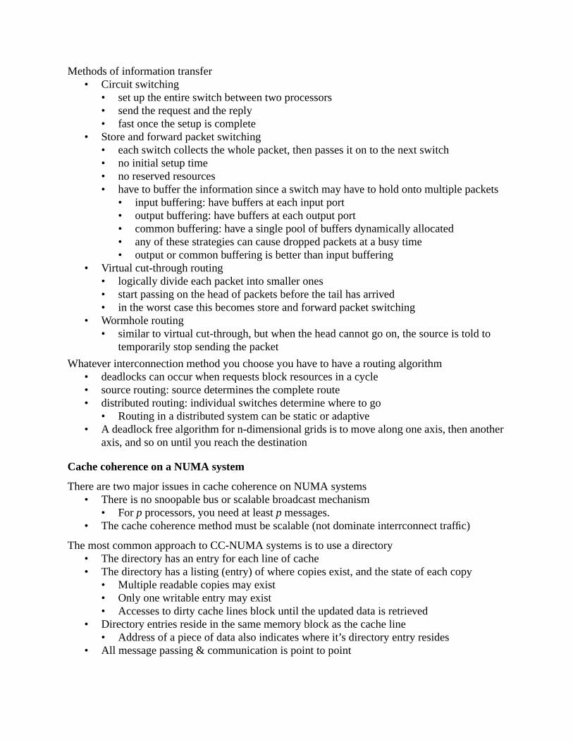
Methods of information transfer• Circuit switching
• set up the entire switch between two processors• send the request and the reply• fast once the setup is complete
• Store and forward packet switching• each switch collects the whole packet, then passes it on to the next switch• no initial setup time• no reserved resources• have to buffer the information since a switch may have to hold onto multiple packets
• input buffering: have buffers at each input port• output buffering: have buffers at each output port• common buffering: have a single pool of buffers dynamically allocated• any of these strategies can cause dropped packets at a busy time• output or common buffering is better than input buffering
• Virtual cut-through routing• logically divide each packet into smaller ones• start passing on the head of packets before the tail has arrived• in the worst case this becomes store and forward packet switching
• Wormhole routing• similar to virtual cut-through, but when the head cannot go on, the source is told to
temporarily stop sending the packet
Whatever interconnection method you choose you have to have a routing algorithm• deadlocks can occur when requests block resources in a cycle• source routing: source determines the complete route• distributed routing: individual switches determine where to go
• Routing in a distributed system can be static or adaptive• A deadlock free algorithm for n-dimensional grids is to move along one axis, then another
axis, and so on until you reach the destination
Cache coherence on a NUMA system
There are two major issues in cache coherence on NUMA systems• There is no snoopable bus or scalable broadcast mechanism
• For p processors, you need at least p messages.• The cache coherence method must be scalable (not dominate interrconnect traffic)
The most common approach to CC-NUMA systems is to use a directory• The directory has an entry for each line of cache• The directory has a listing (entry) of where copies exist, and the state of each copy
• Multiple readable copies may exist• Only one writable entry may exist• Accesses to dirty cache lines block until the updated data is retrieved
• Directory entries reside in the same memory block as the cache line• Address of a piece of data also indicates where it’s directory entry resides
• All message passing & communication is point to point

Note that it is common for NUMA systems to be built from SMP building blocks. The cache coherence protocol within the SMP block can be different than the one between SMP nodes (for example, bus snooping works well). From the point of view of other SMP nodes, however, the memory on a node appears to be a single memory unit.
Directories can maintain knowledge about cache line locations using presence and dirty bits• One presence bit for each processor: indicates processor has a read-only copy• One dirty bit for each processor: indicates processor has a writable copy
• Only one dirty bit should ever be set, so it is possible store this more compactly
Cache read misses• Access the directory location• The directory identifies where the latest version of the data is located
• If any dirty bit is set, the data must come from that processor• If no dirty bit is set, then the memory has the latest version
• The node updates the directory and requests the latest version of the data
Cache write misses or read exclusive operations• The directory identifies where the copies of the cache line are located
• presence bits tell where the copies are• Invalidation (read exclusive) or update (write) transactions need to occur• Since ordering and timing are not guaranteed, replies are necessary before completion
• These transactions are usually the responsibility of the requesting processor• The cache line state is sent along with (write) or instead of (read exclusive) the data
• The presence and dirty bits for the requesting processor are set at the end of the transaction
This type of directory (a flat directory structure) is not scalable because of the directory size• More processors means more directory information and more message passing• Cache-based schemes send the directory information with the cache line and use pointers
to link to multiple copies across processors• Hierarchical schemes distribute the directory information as a tree structure
• Each copy of a cache line is a leaf of the tree• Each node in the tree indicates the directory information for its children (4 bits/line)
COMA systems• All memory is viewed as a set of cache lines• Cache lines do not have a permanent address, but their cache directory entries do• To get a cache line, a processor first has to access that line’s directory entry
• The entry specifies where the line is currently located (could be in multiple locations)• There must be some way to invalidate old copies (through the directory table)• There must be a master copy that can never be destroyed

E25/CS25 Lecture #38 S05
Overall Topic: Cache coherence and synchronization of processes
SMP Parallel Systems and Real Programming Modes
There are many SMP parallel systems available commercially
• IBM S/390 Organization (up to 12 processors)• IBM pSeries 690 (up to 32 processors)• Sun E10000 Server (up to 64 processors)
SMP systems use some variation on the MESI protocol to maintain coherence by bus snooping
• Processors must have exclusive access to a shared cache line before writing to it• Standard Read: other processors indicate if they have a copy• Read Exclusive: tells other processors to dump their copy
• In both cases, the latest value may come from another processor rather than memory
Synchronization of processes
Given a snooping cache coherence protocol, we can now think about how best to implement real programming modes like shared variables and barriers using a bus and a shared memory.
• Shared variables need some kind of locking mechanism• Barriers tell asynchronous threads to halt until all processes have reached the barrier.
A synchronization event has 3 parts• Acquire method: a process needs to access a shared variable and enter its critical section• Waiting algorithm: a process may have to wait for access to the variable• Release method: a process has to release the variable and exit its critical section
Synchronization methods can be implemented in hardware or software• From the point of view of most users, they consist of system calls• They sit on the boundary of hardware/software, and this is a case of the hardware provid-
ing explicit OS support for parallel processing
Programs, locks, and barriers sit on top of snooping protocols, so how do we implement them?
Mutual Exclusion
A process wants to lock a variable, modify it, and then release it• Many different synchronization strategies can be implemented with this concept
A simple software lock will fail without an atomic method of comparing and conditionally setting a value in memory (a flag, for example).
while(flag == 1) while(flag == 1)/* wait */; /* wait */;
flag = 1; flag = 1;Variable = new value; Variable = new value;flag = 0; flag = 0;

The problem is that both processes could read flag = 0 and move into the critical section.
Exercise: • Start with one process holding the flag, and then it lets it go & invalidates everyone else• Everyone tries to access flag, then gets in line to modify flag, then moves on
Test&set: a single atomic instruction that writes a 1 to a flag and puts its old value in a register.• The program simultaneously tests the register to see if the old value was 0
• If the value was 0, it can proceed with the critical section (the memory flag is now 1)• If the value was 1, then someone else had the variable and the process must loop
test&set(flag, r0) test&set(flag, r0)while(r0 == 1) while(r0 == 1)
test&set(flag, r0); test&set(flag, r0);
Variable = new value; Variable = new value;flag = 0; flag = 0;
In this case, if the flag is 0, then one process will hit the test&set first and the flag will be set to 1 by the time the other process reads it. If the flag is 1, then both processes will spin on the test&set instruction. Only one process will be the first to read a 0 flag, and will simultaneously set it to 1.
You can do the same kind of operation with a swap command (switches a register with the mem-ory location) or with a fetch&op instruction (fetches the memory location, executes an operation on it like increment or decrement, and writes it back in a single atomic operation).
The problem with a simple test&set is performance (bus traffic)• If lots of processes are waiting in a loop testing and setting the flag, then each time a pro-
cessor hits the test&set instruction all the processor’s caches are invalided and they all have to load them again each time through the loop.
Exercise:• Start with one process holding the flag• Everyone is looping on test & set• Each time a process executes a test & set it invalidates everyone’s cache (call them out)
Enhancement #1: test&set with backoff• wait exponentially longer each time a test&set operation fails• this is not really a fair algorithm, since the process that just released it doesn’t back off
Exercise:• Start with a process holding the flag• If they fail, wait 30 seconds, wait 30 seconds more on each failure• Call out cache invalidations
Enhancement #2: test and test&set• Just do a regular read on the flag first• Only execute the test&set if the regular read succeeds• This reduces the overall bus traffic because the initial reads are in cache• When the lock is released, then there is signfiicant bus traffic as all caches are invalidated
• Could solve this by updating a local cache if somone else is reading the same line

Exercise:• Start with a process holding the flag• Processes get to load the flag value into their local caches• Call out cache invalidations
Ideally, we want:• Low latency• Low traffic• Scalability• Low storage cost• Fairness
test and test&set hits on most of these (low latency, pretty low traffic, low storage cost, scalable (for a bus system). It’s not fair, however.
Load-locked, Store Conditional• Divide the test into two parts
• The load-locked instruction loads a value and sets a flag in the local cache controller• The store-conditional stores the value only if it hasn’t been changed since the last load-
locked instruction• This has the benefit of low traffic on the read aspect (value should be in cache)• This also benefits from the fact that a write doesn’t happen if the value has changed• You can also implement arbitrary fetch&op commands with LL-SC
for(;;) { for(;;) {LL(variable, r1) LL(variable, r1)r1 = new value r1 = new valueSC(variable, r1) SC(variable, r1)if(successful) if(successful)
break; break;} }
A simple LL-SC lock is nice except:• When a processor successfully writes, everyone rushes to grab it (their caches are invali-
dated by the write to the flag)• It isn’t fair because some processor could be privileged in the race to update the caches
Exercise:• All processes try to load-lock a value and modify it• The first one to succeed in writing it invalidates all other caches, who have to start again• Processes try to repreatedly modify the value
Enhancement #1: ticket-lock• Have a variable that provides tickets
• Each processor takes the current value as its ticket then increments the ticket provider• Use a LL-SC process to manage the ticket provider (fetch & increment)
• Have a variable that specifies who has access to the critical variable(s) • Each processor watches the now-serving variable• When the processor’s ticket matches the now-serving variable, it gets to proceed• Upon leaving the critical section, the processor increments the now-serving variable

• Problem is that all processors still rush the now-serving variable when it changes• Could have processors wait proportional to the difference between their ticket and the
now-serving variable• Could have processors update their caches from other processor’s read misses
Exercise:• Need three memory locations• “Ticket server” functions using the LL-SC protocol• “Now serving” functions using standard cache reading & invalidation• “Critical variable” functions using standard cache reading & invalidation
Enhancement #2: Array-based lock• Each processor gets its own entry in a now-serving array• Ticket variable metes out locations in the array as with the ticket-lock approach
• The array should be a circular buffer with entries on different cache lines• Each processor watches only its location in the array• Upon leaving its critical section, a processor must reset its own flag and set the next in line
For array-based locks, the traffic is pretty much constant with the number of processors
Ticket-lock with proportional delay also works well.
Exercise:• Need lots of memory locations (physical spaces)• “Ticket server” doles out locations using the LL-SC protocol• Processes move the flag along to different locations after they finish the critical section