Embed Size (px)
Citation preview

International Journal of VLSI design & Communication Systems (VLSICS) Vol.7, No.3, June 2016
DOI : 10.5121/vlsic.2016.7303 29
DESIGNING AN EFFICIENT APPROACH FOR JK
AND T FLIP-FLOP WITH POWER DISSIPATION ANALYSIS USING QCA
Shraddha Pandey, Sonali Singh and Subodh Wairya
Department of Electronics,
Institute of Engineering and Technology, Lucknow, 226021, U.P, India
ABSTRACT
QCA (Quantum Dot Cellular Automata) is an emerging and pioneer technology, which is a paradigm for
computing with interacting quantum dots. Many eminent researchers have well thought of eloquent work in
the existing areas of the sequential circuit. However, this paper proclaims three new approaches to design
JK and T flip-flop. Since flip-flops and memory design are the crucial building blocks of digital circuits,
therefore we concern the underlying principle of fundamental design of JK and T flip-flop and then work
out to model the new structure favorable with the forthcoming excellence required. This new concept
places elsewhere the need of using feedback path in flip flop design. Also two algorithms have been shown
for explanatory purpose. The proposed structure is able to establish the validity and genuineness than
earlier design. By using the proposed T flip-flop, a 2-bit and 3-bit counter is also designed in the paper.
The simulation result of the proposed design proves their vigorousness and correctness in the output.
KEYWORDS
Quantum-dot cellular automata (QCA), Level triggered flip-flop, Counter, Kink energy, Thermal hot spots,
Nanometre scale.
1. INTRODUCTION
According to Moore’s law, it is observed that over the history of computing hardware the number
of transistors in a dense integrated circuit has doubled approximately every two years. But
computing hardware the number of transistors in a dense integrated circuit has doubled
approximately every two years. But at nano regimes, computation is substantially different from
conventional VLSI. The current CMOS technology is going to face a scaling limit in deep
nanometres technologies. In order to overcome the physical limitation of MOSFET based VLSI
circuit design, such as tunnelling currents, sub-threshold leakage, quantum effects , fabrication
cost, interconnect delay, the researchers are now focusing on developing a new technology that
uses quantum mechanics and cellular automata simultaneously. And thus, QCA (Quantum Dot
Cellular Automata) is the best replacement of the CMOS based VLSI design. It is a novel
nanotechnology which promises extra low power, extremely dense and very high-speed structure
for designing any arbitrary function at the nanoscale [1]. In 1993, Lent.et al. proposed a physical
implementation of an automation using quantum-dot cells.
The automation quickly gained popularity and it was first fabricated in 1997 [2]. With the use of
QCA technology, new physical phenomena such as Coulombic interactions can be exploited. As

International Journal of VLSI design & Communication Systems (VLSICS) Vol.7, No.3, June 2016
30
there is no electrical current in QCA, signal propagation takes place according to coulomb's law.
For this, a quantum cell is used which is much smaller than transistors and yield better results in
speed. Hence, the electronic devices based on this can become denser. Due to these features
researchers have done much exploration in digital electronics. This field is divided into two
categories; combinational and sequential circuits. In QCA, both the circuits are implemented
efficiently. By using the same Boolean logic functions used in the conventional CMOS circuits,
the combinational circuits are directly implemented. But in order to design sequential circuits, the
truth table is identified and then the Boolean logic equations are derived. Finally, the sequential
circuit is designed by using the derived equations. A number of QCA based logic circuits with
remarkable advantage have been proposed with the utilization of QCA. A number of
combinational circuits such as adders [3], ex-or gate and multiplexer circuit [4], decoders [5] are
proposed. However sequential circuit design in QCA is still in its inception and limited studies
are reported, such as memory circuits [6, 7]. Using QCA memory cells to implement sequential
elements, however, would be difficult in terms of hardware and latency [8], so the design and
application of RS, D, JK and T flip-flop have gained much attention. This paper consists of 6
parts. Part 2 includes the basic concept of QCA and the fundamental circuits used to design any
complex circuit. We have introduced the clocking schemes used in QCA in the same part. In part
3, a state of the art is shown on the fundamental designs and then the proposed circuits of JK and
T flip-flop architectures are shown which prove its benefits in total consumed area and the
number of cells used. In the same section, we have discussed a novel approach to design a T flip-
flop and its algorithm. Part 4 reveals the application of proposed flip-flops in counter design. Part
5 elaborates power dissipation analysis of the proposed circuit and the simulation result of all the
proposed circuits is demonstrated. Finally, the paper is concluded in part 6.
2. QCA PRELIMINARIES
In this section, the building unit i.e. QCA cell, general logic, and gates in QCA are investigated in
the order of QCA cell, QCA wires, majority gates, inverter, AND-OR gates.
2.1 QCA Cell
The primitive cell in QCA technology, as shown in Fig.1 (a), is a square-shaped cell. It contains
four quantum dots at each corner of the cell. The quantum dot normally contains two electrons in
each cell, which occupy two dots of the cell. Due to the Coulombic repulsion between the
electrons, the electrons tend to occupy the position which has lower repulsion force between them
and electrons can occupy stable states. Hence, they occupy the diagonal position within the cell.
There are two methods possible for the placement of electrons as shown in Fig.1 (b). Therefore,
two polarities are possible. If the electrons occupy the position as shown in Fig.1 (b) then it
corresponds to polarization "1" i.e. logic 1 and if is arranged as shown in Fig.1(c) then it is in
polarization "-1" i.e. logic 0 states. These 2 extra mobile electrons can quantum mechanically
tunnel between dots, but not cells.
(a) QCA cell empty (b) 1 polarity (c) 0 polarity
Fig.1 QCA cell

International Journal of VLSI design & Communication Systems (VLSICS) Vol.7, No.3, June 2016
31
Hence unlike conventional digital circuits in which information is passed by the flow of electric
current, QCA operates by the Coulombic interaction that connects the state of one cell to its
neighbor cell state.
2.2 QCA wire and types
In order to transmit the information from one cell to another, a QCA wire is needed. The wire
consists of a chain of cells where the cells are also coupled to each other. The logic values are
passed from one cell to the next cell due to the coulomb interaction. The polarization of the input
cell is traveled down the wire. As a result, the arranged system attempt to settle down to a ground
state. Due to electron repulsion if the polarization of one cell changes, it enforces its adjacent
cells to change its state as shown in Fig.2.
Fig.2 QCA Wire
The way of placing quantum dots in the square cell make it possible to have two types of
orientation. The first one is called as 90° wire and the second is 45° as shown in Fig.3(a) and 3(b)
in which every other cell with opposite polarity is put together.
(a) 90° wire (b) 45° Wire
Fig.3 QCA wire types
2.3 Majority gate
Majority gate is one of the fundamental gates of QCA. It is shown in Fig.4 which is a 3-input
majority function. The output is simply the majority of the 3 inputs applied. Assuming the inputs
is A, B, and C, the Boolean function of the majority gate is,

International Journal of VLSI design & Communication Systems (VLSICS) Vol.7, No.3, June 2016
32
M (A, B, C) = AB+AC+BC (1)
Now if we fix the polarization of one input to logic “0”, say B, then equation (1) can be equated
as follows:
M (A, 0, C) = A.0+AC+0 = AC (2)
Hence equation (2) is simply the AND operation between A and C input. Similarly if we put the
input B value equals to “1” then,
M (A, 1, C) = A.1+AC+1.C = A+C+AC = A (1+C) +C = A+C (3)
Equation (3) is an OR operation between A and C. Thus by changing the value of any of the
input, the 3-input majority gate can function as AND gate and OR gate.
Fig.4 Majority Gate Structure [9] Fig. 5 (a) Inverter
2.4 Inverter gate
There are multiple ways to do it in the QCA paradigm that one is shown in Fig.5.In fig. (a), the
signal comes from the left, splits into two parallel wires, and is inverted at the point of
convergence [11]. The other arrangement used to make inverter chain as shown in Fig.5 (b) and 5
(c).
(b) (c)
Fig.5 (a), (b), (c) Three different way to make inverter in QCA
However, placement of two cells such that they approach via only one corner leads to switch
from -1 logic to +1 logic or vice versa as shown in Fig.5(b).
2.5 QCA clocking scheme
In VLSI design, the function is controlled by a clock signal which is inherent to the technology
used. In contrast to this, QCA exhibit clocking scheme as the most fundamental concept to
understand. As we know there is no flow of any current signal in the propagation of information
in QCA, this does not actually means that power dissipation must be zero. Clocking in QCA not

International Journal of VLSI design & Communication Systems (VLSICS) Vol.7, No.3, June 2016
33
only confer control of information flow but also true power gain in QCA [10]. The signal energy
forfeited to the environment is restored by the clock used.
Clocking in QCA is accomplished by two types of switching methods for its operation: abrupt
switching and adiabatic switching. In abrupt switching, the inputs changes suddenly and the
circuit can be in some excited state; consequently, the QCA circuit is relaxed to ground state by
dissipating energy to the environment [11]. This inelastic relaxation is ungoverned and the QCA
circuit may inscribe a metastable state that is deduced by a local, rather than a global energy
ground state. Therefore, adiabatic switching is usually preferred; in adiabatic switching, the
system is always kept in its instantaneous ground state [11].
After applying the clock signal, the electrons may either pushed to the four corner dots or pull
them into the two middle dots. When the electrons are in the middle dots, the cell is said to be in
the "null" state and when the electrons are in the four corner dots, the cell is in an active state.
The cell in an active state is used to represents binary "0" and "1" values as shown in fig.1. This
clocking scheme (which was recommended in [11] consists of four phases: Switch, Hold,
Release, and Relax, as shown in Fig.6 (a).
(a) Four phase clocking (b) Switching of signal
Fig.6 Clocking in QCA
All cells in a zone are controlled by the same clock signal. Cells in each zone perform a particular
calculation. During the Relax phase, the electrons are pulled into the middle dots, and the cell is
in "null" state. During the Switch phase, the interdot barrier is leisurely raised and pushes the
electrons into the corner dots, so the cell acquires a definitive polarity under the dominance of its
neighbors (which are in the Hold phase). The operation of fig.6 (b) is summarized below:
• During the first clock phase, the switch phase, the inter-dot potential barriers are low.
The barriers are then raised during this phase and the QCA cells become polarized
according to the state of their driver (i.e. their input cell).It is in this clock phase that the
actual computation occurs. By the end of this clock phase, barriers are high enough to
suppress any electron tunneling and cell states are fixed.
• During the second clock phase, the hold phase, barriers are held high so the outputs of the
sub-array can be used as inputs to the next stage.
• In the third clock phase, the release phase, barriers are lowered and cells are allowed to
relax to an unpolarized state.

International Journal of VLSI design & Communication Systems (VLSICS) Vol.7, No.3, June 2016
34
Finally, during the fourth clock phase, the relax phase, cell barriers remain lowered and cells
remain in an unpolarized state.
3. STATE OF THE ART
Many prominent researchers are in strong progression and building sturdily in the existing areas
of the sequential circuit. However, new methods are developed in order to challenge the existing
designs and promising in terms of efficiency. In QCA, the research in the sequential circuit is still
unveiled and due to this many concepts to design the same logic is in current trend in this field.
A novel structure of falling edge triggered clock is shown by Xiaokuo Yang in [20]. He has
suggested using edge-triggered clocking scheme in place of level triggered as used by J. Huang
[13] to design S-R flip flop. He said that when we design a JK flip-flop using the concept of J.
Huang, we would have a race-round condition. One of the proposed circuits of falling edge
triggered clock of reference [20] is shown below.
Fig.8 QCA layout of falling edge-triggered [20]
By using this circuit, JK flip-flop is constructed which uses 7 majority gates and 5 inverters.
Also, 2-bit and 3-bit counters are then proposed by using the circuit of falling edge triggered JK
flip-flop. By looking at the output of truth table, the output is simply AND operation between the
clock input and its delayed version.
Table 1: Truth table of Fig.8 [20]
One more researcher Lin-rong XIAO in [8] has shown method of dual edge triggered clocking
scheme by using 1 latch and 1 mux only. By using this he has proposed two new QCA model of
JK and D flip-flop. The output is obtained after four clock cycles.Lee Ai Lim and others in [21]
have gone through all the flip-flops and its application to design counter in their paper. In his
CP
CP CP_OLD OUTPUT
(AND)
1
1 0
0
0 1
0
1
1
0
1
1
0
0
0
1
0
0

International Journal of VLSI design & Communication Systems (VLSICS) Vol.7, No.3, June 2016
35
paper, JK flip-flop uses 4 majority gates and three inverters. However, the QCA equivalent based
on the equations of Lee Ai Lim is not competent regarding a number of cells required to
formulate the objective. Hence, it is required to design a competent circuit which manifests
robustness and adeptness.
Sequential circuit plays a very important role in the designing of digital circuits. By using
combinational circuit only those applications are covered successfully which depends on their
present state only. Sequential circuits depend not only on their present state but also on past state.
To design sequential circuits, the conventional CMOS circuits are not suitable to direct translated
into QCA architecture due to timing constraint of the sequential logic circuits [21]. Therefore,
each sequential circuit has been derived by using the truth table and then related Boolean
equation is mentioned. Each variable is named as input and output function. Then the number of
required logic gates is determined.
3.1 JK flip-flop
A JK flip-flop is the modification of SR flip-flop. The only difference is that the intermediate
state is more refined and precise than that of an SR flip-flop. The behaviour of inputs J and K is
same as the S and R inputs of the SR flip-flop. The letter J stands for SET and the letter K stands
for CLEAR. The block diagram of JK flip-flop by using SR flip-flop is shown in Fig.9 and the
truth table in Table 2. Table 2: Truth Table of JK Flip-Flop
Fig.9 JK Flip-Flop
Also, the JK flip-flop using NAND latch is shown in Fig.10.The QCA equivalent of cross-
coupled gates is not possible. Hence, it is required to create some feedback paths to achieve this
concept.
Fig.10 JK Flip-Flop Using NAND Latch

International Journal of VLSI design & Communication Systems (VLSICS) Vol.7, No.3, June 2016
36
3.2 T flip-flop This is a much simplistic version of the J-K flip-flop. Both the J and K inputs are connected
together and thus are also called a single input J-K flip-flop. When the clock pulse is given to the
flip-flop, the output begins to toggle which is half of the frequency of input T. It is useful for
constructing binary counters, frequency dividers, and general binary addition. The truth table is
discussed below.
Table 3: TFF Truth Table
One of the researcher in [21] have proposed a falling edge triggered JK flip-flop based on which
a T flip flop is designed as shown in fig 11. The working principle of this design is somewhat
similar to the proposed structure of [21] but it will use crossover technique to implement in QCA.
Here a falling edge triggered clock is used as a second input to T flip-flop. The QCA equivalent
block diagram is shown in Fig.11.
Fig.11: Approach to design T flip flop
The majority equation for the above circuit can be written as:
Q1+n
= M(M(M(M(T, nQ ,0), M(T̅,Qn
,0),1)), CLK,0), M(CLK ,Q1+n
,0),1)
= M(M(( nnQTQT .. + ), CLK,0), (CLK .Q
1+n), 1)
= ( nnQTQT .. + ).CLK + CLK .Q
1+n

International Journal of VLSI design & Communication Systems (VLSICS) Vol.7, No.3, June 2016
37
3.3 Proposed Design of JK Flip-Flop When J and K are in HIGH state, the flip-flop switches to the complement value of previous
output. The proposed JK flip-flop is controlled by using a clock and thus it is called as positive
level triggered JK flip-flop because output will change its state only when the clock will be in
HIGH state. The truth table of the proposed circuit is shown in Table 4.
Table.4 Truth Table of Proposed Level Triggered JK Flip-Flop
From the above truth table, we can write the expression for Q1+n
by going through the following
algorithm as below:
Algorithm 1: Level triggered JK flip-flop
Input: A, B, C where
A= J;
B=K;
C=CLOCK;
Output: Q n , Q1+n
, where Q n = previous output and Q1+n
= present output
(To set the value of inputs, we take the vector form as)
Set input ((A, B, C) & output (Q n ))
A = 0, 1;
B = 0, 1;
C = 0, 1;
Q n = 0;
Set variable i= 0 to n; (for the number of combination)
begin
for( i= 0; i≤7; i++)
{
if (C=1)
{
for

International Journal of VLSI design & Communication Systems (VLSICS) Vol.7, No.3, June 2016
38
A=B=0; Q1+n
= Q n ;
A=0; B=1; Q1+n
=0;
A=1; B=0; Q1+n
=1;
A=1; B=1; Q1+n
= nQ ;
}
else
{
Q1+n
= Q n ;
}
}
Fig. 12 (a) Block Diagram of proposed level triggered JK flip-flop
Fig. 12 (b) Layout of proposed level triggered JK flip-flop

International Journal of VLSI design & Communication Systems (VLSICS) Vol.7, No.3, June 2016
39
The majority logic equation can be derived by observing the above block diagram as follows:
Q1+n
= M(M(M(K, CLK ,0),M( K ,CLK,0),1),J,0))
= M(M((K. CLK ),( K .CLK),1),J,0)
= M(( CLKKCLKK ... + ),J,0)
Operation:
1) J=K=0: When both the inputs are in LOW state then the output follows its previous value. It
means if the previous state is in the low state then the present output is also low and vice-
versa.
2) J=0, K=1: The output must be equal to ‘0' if the clock value is in the high state. If it is in the
low state then the output simply follows its previous value.
3) J=1, K=0: In this case, the output is equal to ‘1' if the clock value is also high as shown in the
truth table.
4) J=K=1: When both the inputs are equal to ‘1' then the output is equal to the compliment of its
previous value only when the clock value is also high.
The above equation i.e. equation 4 is the Boolean expression of the proposed circuit and the
block diagram is shown in Fig.12 (a). The QCA implementation of the proposed circuit is shown
in Fig. 12(b). In contrast with the circuit shown in the paper [8], the proposed scheme uses only 4
majority gates and 2 inverters. Also, the circuit is robust and more efficient in terms of a number
of cells used. The area constraint is one of the major issues in designing digital circuits. This
circuit is very promising related to the total area consumed.
3.4 1st proposed structure of T flip-flop
Sequential circuits deploy flip flops as the memory element. In QCA, memory elements are
formulated by using feedback paths. But according to the truth table 4, the previous output is
acting as an input to get the present value of output. And this is achieved by giving one clock
cycle delay to Q. Fig.13 (b) displays the QCA equivalent of the 1st proposed scheme of T flip-
flop. It comprised of 3 majority gates and 2 inverters only. The output is simply the ex-or
operation between T and the Q. The output is obtained after one clock cycle delay.
Fig. 13 (a) Majority schematic of proposed (b) Layout of proposed T flip flop
T flip flop

International Journal of VLSI design & Communication Systems (VLSICS) Vol.7, No.3, June 2016
40
3.5 The second proposed T flip-flop structure
As described for earlier designs in [7], [13], [21] and 1st proposed scheme, the output is feedback
to the input side and due to this one clock cycle delay is produced in all the prior circuits. In order
to avoid this, a novel structure of T flip-flop is proposed. In this structure, there is no need to give
a feedback path from the output to the input. The clock signal is acting as the second input of the
flip-flop. The clock used here is dual edge triggered type. The truth table for the operation is
shown below.
Table 5: Dual edge triggered clock Table 6: T flip-flop
Algorithm 2: Dual edge triggered T flip-flop
Input (A, B, C) where
A=T;
B=Clk (t-1);
C= Clk (t);
Output (Qn
, Q1+n
) where Q n = previous output and Q1+n
= present output
Set input ((A, B, C) & output (Q n ))
A= 0, 1, X;
B= 0, 1;
C= 0, 1;
Qn = 0;
Set variable i= 0 to n; (for the number of combination)
Transition (Q1+n
)
{
If(Clk(t) = Clk(t-1) = 0/1)
Q1+n
= Qn
;
else
Q1+n
= Qn
for (T = 0); nQQn =+1 for (T = 1);
}
Begin
{ for( i= 0; i≤3; i++)
{
if (C=B);
Q1+n
= Qn
for (A = X);
Clock(t-1) Clock(t) Output
0 0 Not changed
0 1 Changed
1 0 Changed
1 1 Not changed
T CLK Q1+n
0 0 Qn
0 1 Qn
1 0 nQ
1 1 nQ

International Journal of VLSI design & Communication Systems (VLSICS) Vol.7, No.3, June 2016
41
Else Call Transition
}}
Fig.14: (a) 2
nd proposed schematic for T flip-flop (b) QCA equivalent of T flip-flop
Let Qn
= 0 then the majority logic equation can be derived by observing the above block diagram
as follows:
1+nQ = M (T, A, 0),
where A = M (CLK, DCLK’, 0) and DLCK refers to delay in clock
The majority based equivalent diagram of the above equation is shown in Fig.14 (a). In contrast
to the previous design, it consists of only 2 majority gates and 1 inverter. The advantage of this
scheme is that there is no need to create a feedback path from the output side to the input side.
Due to this, there is delay of 0.25 clock cycle in the circuit. The QCA equivalent diagram is
shown in Fig. 14(b) which comprises of 28 cells occupying an area of 0.05���.
4. APPLICATION OF PROPOSED T FLIP-FLOP
4.1 2-Bit Counter:
Using T flip flop and some additional combinational logic circuits, any sequential logic design
can be implemented. Counters and registers are the most prominent application in this digital era.
Fig. 15 shows 2-bit counter (mod 4) by using T flip-flop. In this design, two T flip flops and four
AND gates are used. The output of first T flip flop is applied as an input to the second T flip flop.
The output Q0 toggles for every clock cycle. The output Q1 changes only when Q0 changes from
1 to 0. Accordingly a 3-bit counter can also be designed as shown in Fig.16. The clock pulse is
applied as a second input to the majority gate. The output of the first flip-flop is applied to second
flip flop after performing an AND operation with the clock pulse. The output Q0 changes when
the clock pulse remains high.

International Journal of VLSI design & Communication Systems (VLSICS) Vol.7, No.3, June 2016
42
Fig.15 2-bit counter QCA layout
Fig.16 3-bit counter QCA block diagram
5. SIMULATION RESULTS AND DISCUSSION
In this section, the proposed methods are simulated and their correctness has been proved by
using QCADesigner tool. This tool is a type of simulator which simulates the QCA logic
components and reports the result in terms of the input-output state. Additionally the discussion
of power dissipation is elaborated in this section. Based on the simulation result, it is clear that
the proposed design works correctly.
5.1 Power Dissipation Analysis:
In QCA computations, only a few electrons are involved, it is susceptible to thermal issues.
Therefore, power analysis is vital to model as an important parameter to analyze QCA design
process along with errors. The most appropriate comprehension about it was studied well by
J.Timler and C.S.Lent [15]. They have shown power dissipation during 3 events within QCA:
clock power, cell-to-cell power gain, and power dissipation. With the help of these estimates, we
can choose best alternative and parameters among many different designs. The power estimates
computed on a per cell basis can be the sum total to obtain power dissipation for a QCA circuit.
Each cell within a QCA circuit goes through the following three types of events: 1) to
"depolarize" a cell, clock is going from low to high; 2) cells in previous clock zone called as
"switching state"; and 3) clock changing from high to low, latching and holding the cell state to
International Journal of VLSI design & Communication Systems (VLSICS) Vol.7, No.3, June 2016
43
new state. Each of these events is associated with power loss [18].The keen interest in this
discussion is that even during the first and third event the state of the cell would change or not,
power dissipation is there due to clock changing only. This condition is analogous to the
"leakage" power in CMOS circuits. And the power loss due to the second event is simply termed
as "switching" power as it involves the cells actually changing their states. These two
components are inversely related with each other. In QCA, a clock is used as an avenue to lower
and raise energy barriers and provide power to the system.
5.2 Kink energy:
In the study of power dissipation the concept of kink energy is useful to mention. When the
system is stuck at any metastable state, a kink is said to occur. The kink energy Ek
is the energy
required to excite the system from the ground state to the first excited state. It must be greater
than k B T to set apart a bit value from the thermal environment where T is temperature in degrees
Kelvin and k B is Boltzmann’s constant. In [15] they have proved that to defend against kink the
number of QCA cells i.e. N in the longest line must be less than ���
�� . .
To do this work a novel
probabilistic modelling tool called as QCAPro is developed by the authors in [16]. To do the
estimation of highly spurious cells in QCA circuit, this technique uses a fast approximation
analysis. Since kink energy relates itself inversely with steady state polarization error and directly
with power dissipation so it is required to choose an optimal value of kink energy. In this paper,
the power dissipation analysis of first proposed T flip-flop is discussed only and then it is
compared with the existing MOSFET technologies. The same approach can be applied to the
much complex circuits as well. According to the analysis observed using QCAPro, we can
choose the best alternative among the available technologies to design a circuit. By varying the
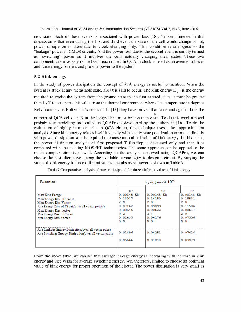
value of kink energy to three different values, the observed power is shown in Table 7.
Table 7 Comparative analysis of power dissipated for three different values of kink energy
From the above table, we can see that average leakage energy is increasing with increase in kink
energy and vice versa for average switching energy. We, therefore, limited to choose an optimum
value of kink energy for proper operation of the circuit. The power dissipation is very small as

International Journal of VLSI design & Communication Systems (VLSICS) Vol.7, No.3, June 2016
44
compared to the conventional Mosfet technologies. Thus, our proposed circuit is meeting the
current demand for the immediate present designs in other paper.
5.3 Thermal layout:
The researchers in [17] have evaluated the consumed power of the circuit using QCAPro which
reveals the design at three different tunnelling energy levels (0.5 Ek, 1Ek, 1.5 Ek) at 2K
temperature. The thermal layout of the T flip-flop is shown in Fig.17. The cells in dark colour
indicate that it is dissipating higher power. And it is called as the thermal hotspot. The total
power dissipation is divided into leakage and switching energies as shown in Table 7. The cells at
the input side are dissipating very low power.
Fig.17 Thermal layout of proposed T flip-flop
Fig. 18: Graph between energy dissipation and kink energy
5.4 Variation of energy dissipation with kink energy:
As the value of kink energy is increased gradually from 0.5 to 1.5, the average energy dissipation
factor goes on increasing as shown in Fig.18. It means it varies linearly with kink energy. The
average leakage energy also follows a linear relationship with kink energy. Hence, an optimum
value of kink energy is chosen to operate the circuit so as to deliver the advantage correctly. In
contrast to this, the average switching energy dissipation shows a decreasing ramp with
increasing value of kink energy. It is, therefore, there is a trade-off between the power dissipation
and the value of kink energy.

International Journal of VLSI design & Communication Systems (VLSICS) Vol.7, No.3, June 2016
45
5.5 Results and Discussion:
A. Output waveform of proposed level triggered JK flip-flop
The output of Fig.12 (b) is verified correctly after seeing the simulation results. The results are
valid only when the clock input is held high. Therefore, the output does not go to SET state even
when J and K are in the high state. It is worth mentioning to revise again that it occurs because
the clock pulse is not high in that input condition. Hence, the circuit changes its state only when
the clock is enabled. There is a delay of one clock cycle between input and output which is
superior as compared to the design in [20].
B. Output waveform of 1st proposed T flip-flop
This is the output of first propose design of T flip-flop shown in fig. 13(b). The output toggles
after one clock cycle delay when T becomes high. The number of cells reduced to a small extent
as compared with reference [21]. The disadvantage of this circuit is that there is no control of
clock in its operation. Thus, a more conventional approach is required
C. Output waveform of 2nd proposed T flip-flop
This is the output waveform of 2nd proposed T flip-flop shown in fig.14 (b). This is a novel
concept of implementing T flip-flop. This circuit has many advantages as compared to the
existing designs till now. Firstly it does not require creating a feedback path from the output to
the input side. Secondly, the number of cells used is very less and hence the area occupied is only
about 0.05���. And at last, we can see the output is obtained even before the one cycle of clock
completes. Hence, delay between input and output is even less than one cycle. The output toggles
only when the clock makes a transition from 1 to 0 or 0 to 1 as shown in the simulation result.

International Journal of VLSI design & Communication Systems (VLSICS) Vol.7, No.3, June 2016
46
D. Output waveform of 2-bit counter
This is the output of 2-bit counter shown in Fig.15.This is a mod(N) counter where N= number of
states obtained and given as:
N ≤ 2n ; where n = a number of flip flops.
Therefore, we obtained four numbers of states at the output as the number of the flip-flop used is
two.
This counter uses only 92 cells to give valid output and the delay is only two clock cycle.
Table 8 Comparison of different implementations
The implementation of JK flip-flop is shown in Fig.12 (b) uses only 54 cells which improve
around 32% as compared to the previous designs. The second proposed method of T flip-flop in
which output toggles when input T is high. It, therefore, gives its output after one clock delay as
International Journal of VLSI design & Communication Systems (VLSICS) Vol.7, No.3, June 2016
47
its present output depends on the value of the previous one. The third proposed model includes
the effect of the clock on the output of T flip-flop. In this case, the output toggles only when the
clock input goes from 1 to 0. This approach is based on a new concept of avoiding feedback from
output to the input side. The fourth QCA model for T flip flop is just an approach used by Xiao
Kou Yang in [21].
6. CONCLUSIONS
The flip-flop is the backbone circuit to design sequential logical functions. This paper has
proposed falling edge triggered and positive level triggered methods of designing flip flops. Later
on, these designs are further expanded to obtain 2-bit and 3-bit counter circuits which are a very
demanding application in the digital world. Simulation results approve the existence of proposed
designs. The new approach of designing T flip-flop is attractive in terms of a number of cells
used and the concept of removing feedback paths. But still many questions on sequential circuits
is required to explore and answer so as to design QCA at large scale application.
REFERENCES [1] P.D. Tougaw, C.S. Lent (1994) “Logical devices implemented using quantum cellular automata”,
Appl. Phys. Vol. 75, pp.1818-1824.
[2] C. Lent, P. Tougaw, and W. Porod (1994) “Quantum cellular automata: the physics of computing
with arrays of quantum dot molecule”, Physics and Computation Proceedings Workshop, vol. 94, ,
pp. 5-13.
[3] Amir Mokhtar Chabi, Samira Sayedsalehi, Shaahin Angizi, and Keivan Navi (2014) “Efficient
exclusive-or and multiplexer circuit based on a nanoelectric-compatible deigning approach”,
Hindawi publishing Corporation, pp. 1-9.
[4] Shaahin Angizi, Esam Alkaldy, Nader Bagherzadeh, and Keivan Navi (2014) “Novel robust single
layer wire crossing approach for exclusive-or sum of products logic design with QCA”, Journal Of
Low Power Electronics, Vol. 10, pp.259–271.
[5] Kondwani Makanda, Jun-Cheol Jeon (2013) “Improvement of quantum dot cellular automata decoder
uing inverter chain”, Advanced Science and Technology Letters, Vol.29, pp.227-229,.
[6] Mohammad Reza Raaei Moghaddam, Ali Akbar Khazaei, Davoud Bahrepour (2014) “Designing an
improved asynchronous memory based on qca”, 9th Symposium on Advances in Science and
Technology, Mashad,Iran..
[7] Mostafa Abdollahian Dehkordi , Abbas Shahini Shamsabadi, Behrouz Shahgholi Ghahfarokhi ,Abbas
Vafaei (2011) “Novel RAM cell designs based on inherent capabilities of quantum-dot cellular
automata”, Microelectronics Journal 42 pp.701–708.
[8] Lin-rong XIAO, Xie-xiong CHEN, Shi-yan YING (2012) “Design of dual-edge triggered flip flops
based on quantum-dot cellular automata”, Journal of Zhejiang University-SCIENCE C (Computers &
Electronics), volume 13(5) pp.385-392.
[9] W.Wang, K.Walus, J.Julien (2003) “Quantum dot cellular automata adders”, Third IEEE Conference
on Nanotechnology, IEEE-NANO, pp. 461-464.
[10] Lent, C. S. and B. Isaksen (2003) “Clocked Molecular Quantum-Dot Cellular Automata”, IEEE
Transactions on Electron Devices, Vol. 50, No. 9, pp. 1890-1895.
[11] Lent, C. S. and P. D. Tougaw (1997) “A device architecture for computing with quantum dots” ,Proc.
Of the IEEE, Vol. 85, pp. 541-557.
[12] K.Navi, M.Moayeri, R.Faghih Mirzae, O.Hashemipour, B.Mazloom Nezhad (2009) “Two new low
power full adder based on majority-not gate”, Microelectronics Journal, 40 (1) pp.126-130.
[13] Abbas Shahini Shamsabadi, Behrouz Shahgholi Ghahfarokhi, Kamran Zamanifar, Naser
Movahedinia (2009) “Applying inherent capabilities of quantum-dot cellular automata to design:D
flip- flop case study”, Journal of Systems Architecture 55 pp.180–187.

International Journal of VLSI design & Communication Systems (VLSICS) Vol.7, No.3, June 2016
48
[14] J. Huang, M. Momenzadeh, F. Lombardi (2007) “Design of sequential circuits by quantum-dot
cellular automata” Microelectronics Journal 38 pp.525–537.
[15] John Timler and Craig S. Lent (2002) “Power gain and dissipation in quantum-dot cellular
automata”, Journal of applied physics, volume 91, issue 2, pp. 823-831 .
[16] Jing Huang, Fabrizio Lombardi (2008) “Design and test of digital circuits by quantum dot cellular
automata”, Boston, MA .
[17] Saket Sivastava, Arjun Asthana, Sanjukta Bhanja, Sudeep Sarkar (2011) “QCAPro- An Error-power
estimation tool for qca circuit design”, IEEE International Symposium of Circuits and Systems
(ISCAS), Rio de Janeiro, pp. 2377 – 2380.
[18] Shadi Sheikhfaal, Shaahin Angizi, Soheil Sarmadi, Mohammad Hossein Moaiyeri (2015) “Designing
efficient qca logical circuits with power dissipation analysis”, Microelectronics Journal, 46, pp. 462-
471.
[19] Saket Srivastava, Sudeep Sarkar, anjukta Bhanja (2009) “Estimation of upper bound of power
dissipation in qca circuits”, IEEE Transactions on Nanotechnology, volume 8 (1), pp.116-127.
[20] Bibhash Sen, Mrinal Goswami, Subhra Mazumdar, Biplab K Sikdar (2015) “Towards modular design
of reliable quantum-dot cellular automata logic circuit using multiplexers”, Computers and Electrical
Engineering, Elsevier vol.45, pp.42–54.
[21] Xiaokou Yang, Li Cai, Xiaohui Zhao, Nansheng Zhang (2010) “Design and simulation of sequential
circuits in quantum dot cellular automata: falling edge-triggered flip flop and counter study”,
Microelectronics Journal 41, pp. 56-63.
[22] Lee Ai Lim, Azrul Ghazali, Sarah Chan Tji Yan, Chau Chein Fat (2012) “Sequential circuit design
using quantum-dot cellular automata (QCA)”, IEEE Conference, Kajang, Selangor, Malaysia 978-1-
4673-3119.
[23] Mohammad Torabi (2011) “A new architecture for T flip flop using qca”, 3rd Asia Symposium on
Quality Electronic Design 978-1-4577-0144, pp. 296-300.
AUTHORS
Shraddha Pandey received the B. Tech degree in Electronics and Communication
from the Bhabha Institute of Technology, Kanpur affiliated to AKTU, Lucknow U.P.,
India, in 2012. She is currently pursuing her M. Tech. in Microelectronics from IET,
Lucknow. Her research interest is in Low power VLSI design, Digital design and
system, Quantum-dot cellular automata and nanoelectronics.
Sonali Singh received the B. Tech degree in Electronics and Communication form the
Bundelkhand Institute of Engineering And Technology, Jhansi, U.P., India in 2013.
She is currently pursuing towards her M. Tech. in Microelectronics from IET,
Lucknow. Her research interest is in VLSI design, Digital circuits and system,
Quantum-dot cellular automata and Nanoelectronics.
Dr. Subodh Wairya received B. Tech (1993), M.Tech and Ph.D (2012) from HBTI,
Kanpur, Jadavpur University, Kolkata and MNNIT Allahbad, India, respectively. His
research area are High speed network, Low power VLSI, Nanoelectronics. Currently,
he is an Professor at IET, lucknow (from 6 May 1996-Present).He has also served as
Scientist “B” Adhoc (One Year) at DRDO, Lucknow during January, 1995-January,
1996 and Graduate Engineer under Consultancy Project at HAL, Lucknow during
From January, 1994-January, 1995 (one year). Also he is one of the authors of a book
entitled “A Simplified Approach to Telecommunication and Electronic Switching Systems” by C.B.L.
Srivastava, Neelam Srivastava & Subodh Wairya Published by Dhanpat Rai and Company in the year
2006.