Embed Size (px)
Citation preview

Dynamic Power Supply Design for High-EfficiencyWireless Transmitters
Jason T. StauthSeth R. Sanders
Electrical Engineering and Computer SciencesUniversity of California at Berkeley
Technical Report No. UCB/EECS-2006-72
http://www.eecs.berkeley.edu/Pubs/TechRpts/2006/EECS-2006-72.html
May 19, 2006

Copyright © 2006, by the author(s).All rights reserved.
Permission to make digital or hard copies of all or part of this work forpersonal or classroom use is granted without fee provided that copies arenot made or distributed for profit or commercial advantage and that copiesbear this notice and the full citation on the first page. To copy otherwise, torepublish, to post on servers or to redistribute to lists, requires prior specificpermission.

Dynamic Power Supply Design for High-Efficiency Wireless Transmitters
by Jason T. Stauth
Masters Research Project
Submitted to the Department of Electrical Engineering and Computer Sciences, University of California at Berkeley, in partial satisfaction of the requirements for the
degree of Master of Science, Plan II.
Approval for the Report and Comprehensive Examination:
Committee:
Professor Seth R. Sanders Research Advisor
(Date)
* * * * * * *
Professor Ali M. Niknejad Second Reader
(Date)


Table of Contents
Chapter 1 Introduction..................................................................................................... 6 1.1.1 Overview..................................................................................................... 7 1.1.2 Previous Work ............................................................................................ 8 1.1.3 Previous Research Summary .................................................................... 13 1.1.4 Research Goal ........................................................................................... 13
Chapter 2 Transmitter Fundamentals ............................................................................ 15 2.1 Broadcast Power Statistics................................................................................ 15 2.2 Power Backoff, Signal Modulation, and the Peak-Average Power Ratio ........ 17 2.3 Role of the PA................................................................................................... 18 2.4 PA Classification .............................................................................................. 20
2.4.1 Linear Classes ........................................................................................... 21 2.4.2 Nonlinear Classes: .................................................................................... 23
2.5 Power Backoff Efficiency................................................................................. 25 Chapter 3 Dynamic Supply Design ............................................................................... 28
3.1 Introduction....................................................................................................... 28 3.1.1 Linear Regulator Dynamic Supply ........................................................... 29 3.1.2 Switching regulator dynamic supply ........................................................ 30
3.2 Switching Regulator Dynamic Supply Design Flow........................................ 31 3.3 Converter Topology.......................................................................................... 33 3.4 Buck Converter Dynamic Supply ..................................................................... 34
3.4.1 Frequency Domain Characteristics and Voltage Ripple........................... 35 3.4.2 PA supply ripple rejection ........................................................................ 36
3.5 Filter Design and Switching Frequency............................................................ 38 3.5.1 LC filter Characteristics............................................................................ 38 3.5.2 Supply Ripple Equations........................................................................... 42 3.5.3 Choosing the Switching Frequency .......................................................... 43
3.6 Power Transistor Sizing and Optimization....................................................... 44 3.6.1 DC-DC Converter Efficiency and the PDF .............................................. 44 3.6.2 DC-DC Converter Efficiency Optimization ............................................. 47 3.6.3 Design Optimization Procedure................................................................ 50
3.7 Power Transistor Sizing Options ...................................................................... 53 3.7.1 Fixed FET Sizing ...................................................................................... 53 3.7.2 Active FET Sizing..................................................................................... 54 3.7.3 Active-Clamped FET Sizing..................................................................... 54 3.7.4 Comparison of Sizing Methods ................................................................ 55
3.8 Design Example: A Dynamic Supply for a WCDMA Class-A PA in 180nm CMOS 57
3.8.1 Matlab Simulation Results........................................................................ 58 3.8.2 Average Efficiency Improvement Ratio ................................................... 59 3.8.3 Effect of Static Bias Power ....................................................................... 60 3.8.4 Conclusion ................................................................................................ 62
Chapter 4 Process and Technology Scaling .................................................................. 63 4.1 Increasing Envelope Bandwidths...................................................................... 63 4.2 CMOS Process Scaling Trends......................................................................... 65 4.3 Scaling Trends Conclusions.............................................................................. 67

Chapter 5 Alternative Topologies and Future Research................................................ 68 5.1 Hybrid Linear-Switching Regulators ................................................................ 68
5.1.1 Parallel shunt transistor............................................................................. 69 5.1.2 Parallel linear-switching regulators .......................................................... 70 5.1.3 Series linear-switching regulators............................................................. 70 5.1.4 Future work............................................................................................... 71
5.2 Multi-Pole Filters .............................................................................................. 72 5.3 Supply Ripple Predistortion.............................................................................. 73
Chapter 6 Conclusion .................................................................................................... 75 References......................................................................................................................... 76
List of Figures
Figure 1.1 Adaptive bias class-A transmitter...................................................................... 9 Figure 1.2 Envelope tracking supply with linear PA........................................................ 10 Figure 1.3 Simplified Kahn EER transmitter.................................................................... 12 Figure 2.1 Representative power distribution function for CDMA applications, from [3,
8] ............................................................................................................................... 15 Figure 2.2 Time domain definition of peak and average voltages.................................... 18 Figure 2.3 Standard wireless transmitter .......................................................................... 18 Figure 2.4 General power amplifier.................................................................................. 20 Figure 2.5 Waveforms and efficiency equations for the linear classes of power amplifier
................................................................................................................................... 21 Figure 2.6 Waveforms and efficiencies for the nonlinear classes of power amplifier ..... 23 Figure 2.7 Ideal Maximum Efficiency vs Output Voltage for Class A, B and Switching
Classes of Amplifier * represents any ideal switching PA: class D, E, or F, and assumes a linear regulator supply is used to scale amplitude ................................... 25
Figure 2.8 a. Efficiency and PDF on a linear scale........................................................... 26 Figure 3.1 Linear regulator dynamic supply..................................................................... 28 Figure 3.2 Linear regulator dynamic supply..................................................................... 29 Figure 3.3 Generalized DC-DC converter ........................................................................ 30 Figure 3.4 Common switching regulator topologies......................................................... 30 Figure 3.5 Dynamic supply design flow........................................................................... 31 Figure 3.6 Representative discharge curves for popular battery technologies, from [32] 33 Figure 3.7 Buck Converter Schematic .............................................................................. 34 Figure 3.8 Dynamic Supply Filter Profile and RF Spectral Mask.................................... 35 Figure 3.9 Real LC Filter with parasitics.......................................................................... 38 Figure 3.10 Root locus and magnitude response for increasing Q with fixed natural
frequency................................................................................................................... 40 Figure 3.11 Comparison of fourier fundamental and small ripple predictions for voltage
ripple (normalized to the maximum amplitude of the ripple fundamental).............. 42 Figure 3.12 Dynamic Supply simulation topology........................................................... 44 Figure 3.13 Efficiency vs output voltage for a resistively loaded DC-DC converter....... 46 Figure 3.14 Power loss vs gate width ............................................................................... 47 Figure 3.15 Optimum PMOS and NMOS width vs Vout (.18um CMOS, fsw=25MHz,
RL=15Ω).................................................................................................................... 49

Figure 3.16 Efficiency vs Output Voltage (example: .18um CMOS, fsw=25MHz, RL=15Ω).................................................................................................................... 50
Figure 3.17 Iteration procedure to calculate maximum total average efficiency ............. 51 Figure 3.18 Contour representation of average efficiency of the switching regulator vs
gate width.................................................................................................................. 52 Figure 3.19 Active FET Sizing Topology: device widths scale with output voltage ....... 53 Figure 3.20 Active-Clamped FET Sizing: Device widths actively scale with vout below
some fixed upper threshold. Threshold is optimized for max average efficiency. .. 55 Figure 3.21 Comparison of possible efficiency differences between FET sizing methods
................................................................................................................................... 55 Figure 3.22 Average efficiency contour plot for gate-width sizing.................................. 58 Figure 3.23 Efficiency vs output power: with and without dynamic supply .................... 59 Figure 3.24 Average efficiency improvement ratio vs power amplifier class and usage
profile (WCDMA supply, 180nm CMOS, Urban PDF) ........................................... 60 Figure 3.25 Average efficiency and AER compared to static power in the handset
(WCDMA supply, 180nm CMOS, Urban PDF)....................................................... 61 Figure 4.1 Efficiency improvement ratio vs carrier envelope bandwidth (.18um CMOS,
Class A PA, supply ripple = 1% of VDD ; Urban PDF from Figure 2.1)................... 64 Figure 4.2 Scaling trends for dynamic supply average efficiency improvement (.18um
CMOS, Class A PA, supply ripple = 1% of VDD , Urban PDF from Figure 2.1) .... 66 Figure 5.1 Comparison of optimized switching regulator and linear regulator solutions 68 Figure 5.2 Representative ‘hybrid’ linear-switching regulator topologies ....................... 69 Figure 5.3 Multi-pole Buck Converter Topologies........................................................... 72 Figure 5.4 Diagram of Ripple Predistortion Architecture ............................................... 73

Chapter 1
Introduction
Much of the commercial growth of wireless technology in recent decades can be
attributed to mobility – the ability to communicate without permanent connection to the
power grid or wireline network. While this aspect of wireless communication has been
improved by advances in battery technology and semiconductor processing, much room
is left for innovation in the radio architecture and circuit design.
An area of emerging importance is the efficiency of wireless transmitters for modulation
standards with varying carrier amplitudes. The use of increasing amounts of amplitude
modulation and cellular system power control are driving average carrier voltages further
below the battery voltage. In this situation wireless transmitters tend to operate with
reduced efficiency. This is because the power amplifier (PA), the output stage of the
transmitter that interfaces with the antenna, is often less efficient when the output signal
amplitude is less than the supply voltage. Ultimately, because traditional power
amplifiers suffer from reduced efficiency at low power levels, these trends are leading to
reduced battery life.
This report addresses the use of novel techniques in power management to reduce the
average power consumption of wireless transmitters which tend to operate at less than
maximum power. It is shown that efficient and rapid adjustment of the supply voltage for
the power amplifier can provide up to an order of magnitude higher average efficiency.
This report presents a design and optimization process for switching regulator supplies
for RF power amplifiers. Inputs to the design process include system constraints such as
the envelope bandwidth, spectral requirements, and the statistics of output power levels.
The result is the optimization of CMOS power switches for a step down (buck) DC-DC
converter and LC filter elements. The switch and filter components are designed to meet
the dynamic response criterion for minimum average power dissipation. Control

coefficients for optimum feedforward or feedback control may then be based on the
dynamics of the power train.
1.1.1 Overview
Power amplifiers universally suffer from reduced efficiency when operated below the
maximum output power as limited by the battery voltage, a condition known as power
backoff [1]. This problem is compounded by the use of high data-rate standards. Higher
data rates tend to require larger amounts of amplitude modulation to increase the number
of bits per symbol [2]. More amplitude modulation increases the peak to average power
ratio (PAR), which is a measure of the peak to average power supplied to the antenna by
the PA. Therefore, as wireless standards evolve, traditional transmitter architectures will
be forced to operate with lower average efficiencies [3].
SystemBandwidth
(MHz)Modulation
Peak-Average Power Ratio
(dB)
Peak-Minimum Power Ratio (dB)
Antenna Power (dBm)
Power Control Range (dB)
1G (AMPS) 0.03 FM 0 0 28 25ANSI-136 0.03 p/4-DQPSK 3.5 19 28 35GSM 0.20 GMSK 0 0 33 30GPRS 0.20 GMSK 0 0 33 30EDGE 0.20 3p/8-8PSK 3.2 17 27 30WCDMA 3.84 HPSK 3.5–7 infinite 24 80IS-95B 1.23 OQPSK 5.5–12 26—infinite 24 73cdma2000 1.23 HPSK 4–9 infinite 24 80Bluetooth 1.0 GFSK 0 0 20 —802.11b 11.0 QPSK 3 infinite 20 —802.11a/g 18.0 OFDM 6–17 infinite 20 —
Table 1 Modulation Standards used in mobile communication devices [4]
Table 1 shows a range of 2G and 3G cellular standards and wireless internet protocols
[4]. Here, the progression of US and European cellular standards from AMPS and GSM
to CDMA-2000 and WCDMA (UMTS) is shown. Wireless internet standards are also
shown to illustrate trends in the peak-average ratio. Other trends shown in Table 1 that
will affect transmitter performance include envelope bandwidths and the power control
range. Higher envelope bandwidths mean that transitions between symbols will happen
at faster rates. This puts pressure on the transmitter, and potentially the power supply to

perform bias adjustments increasingly fast. More power control implies an even wider
dynamic range of operation for the PA. It will be shown in Chapter 2 that without
adjustment of biasing levels in the PA – including dynamic adjustment of the power
supply – the result will be a significant reduction in average power efficiency.
1.2 Previous Work
Application Author PA TypeSupply
RegulatorEnvelope
BandwidthMax
EfficiencyAverage
Efficiency Ref+
Adaptive current biasing
Saleh, Cox (Bell Labs)
Class-A, AB
Fixed Supply - - - [5]
Envelope Tracking
Wang... Asbeck (UCSD) Linear hybrid buck 20MHz 30%* - [11]
Envelope Tracking
Schlumpf...Dehollain (SFIT, Switz) Linear Buck 1.5 MHz 85%** - [10]
Envelope Tracking
Hanington... Larson (UCSD) Linear Boost 1.0 MHz 74%** 6.38%* [6]
Average Power Tracking
Sahu, Rincon-Mora (Georgia Tech) Linear Buck-Boost 1.5 kHz 65%** 6.78%* [8]
Average Power Tracking
Staudinger et al. (Motorola) Linear Buck 500kHz 90%** 11%* [7]
Polar ModulationWang… Popovic (CU Boulder) Class E Buck 12 kHz 60%* - [9]
Polar ModulationOshima, Kobuko (Hitachi) Class E Buck 1.0MHz 30.7%* - [12]
Table 2 Representative publications emphasizing dynamic biasing for PAs [5-12]
+References numbered chronologically by publication date *PA and power converter **Power converter alone
Table 2 highlights publications representative of the scope of previous research related to
dynamic biasing in PAs. This table demonstrates the relevant transmitter architectures
and envelope bandwidths addressed in the literature. A distinction is made between
maximum efficiency and average efficiency. Maximum efficiency is specified only at
maximum power and therefore may not be directly related to battery life. Average
efficiency is a measure of long-term power efficiency and is a function of the statistics of

transmitted power. As discussed by Sevic in [13], average efficiency may be the most
important measure in determining the battery requirements for the transmitter.
This section will discuss the concepts and terminology presented from the prior work
shown in Table 2. The following section will expand on the goal of this project report,
and discuss how this research will expand on the prior art.
1.2.1 Adaptive Current Biasing
There are several available techniques to improve the average efficiency of power
amplifiers. This first is adaptive bias control, a topic discussed by Saleh and Cox in [5].
Figure 1.1 Adaptive bias class-A transmitter
Saleh and Cox proposed to reduce the bias current of Class-A PAs in proportion to the
envelope voltage to improve the average efficiency of Class A and AB amplifiers when
operated in power backoff. Adjusting the bias is beneficial because it reduces the
quiescent current level in the PA. As seen in Figure 1.1, this technique requires some
method of envelope detection or prediction to set the bias level appropriately. While
adjusting the DC current reduces the power drawn from the supply, a constant supply
voltage means that the efficiency of the PA still falls off as the carrier amplitude is
decreased.

1.2.2 Envelope tracking
Figure 1.2 Envelope tracking supply with linear PA
In an envelope tracking system, as seen in Figure 1.2, the PA supply voltage is
dynamically adjusted to the most efficient level for the instantaneous output power level.
This allows the PA to operate near maximum efficiency – even while in power backoff.
To increase the efficiency of the entire transmitter, the power supply must be adjusted
efficiently and rapidly. This requires a fast switching regulator power supply, as in [6,
10, 11].
In [6], Hanington proposed an envelope tracking system for a CDMA transmitter. This
solution was designed to step voltage up from a 3V supply to provide a dynamic supply
at the drain of a gallium arsenide (GaAs) MESFET PA transistor. The supply voltage
was varied synchronously with the carrier envelope to track the supply voltage required
by the linear PA. Average efficiency was reported to increase from 3.89% to 6.38%.
In [10], Schlumpf described a buck converter capable of tracking a 2MHz envelope
bandwidth. The switching frequency was 16 MHz and the instantaneous efficiency was
85% at an output voltage of 1.25 V and 95mA of load current. Sliding-mode (hysteretic)
control was used, which required a large off-chip capacitor and resistor for compensation.
Unfortunately, average efficiency was not reported.
Wang proposed an envelope tracking power amplifier for WLAN 802.11g in [14]. Here,
the supply adjustment was done at frequencies up to 20MHz with a combination of

switching and linear regulators. The total drain efficiency of the transmitter was 30%,
with the supply modulator efficiency of 50-60%.
1.2.3 Average power tracking
Average power tracking is similar to envelope tracking except that the power supply
tracks the average transmitted power. This type of solution may provide substantial
increases in average efficiency for systems with a large power control range but low
peak-average power ratios.
Staudinger proposed an average power tracking dynamic supply in [7]. The supply was
adjusted to track the long term rms envelope signal for a CDMA PA. Average efficiency
was reported to go from 2.2% to 11% with the dynamic supply.
Sahu and Rincon-Mora of Georgia Institute of Technology described an average power
tracking buck-boost supply for CDMA in [8]. The power converter could adjust output
voltage from 0.5-3.6V from a 3.0V supply. Average efficiency of the system was
increased 4.4 times from 1.53% to 6.78% by using a dynamic supply. This solution had a
bandwidth of approximately 2 kHz and was designed to respond to average power
changes within 200uS.
1.2.4 Polar modulation and EER
As will be discussed in Chapter 2, amplitude modulation of nonlinear PAs can be done by
modulating the supply voltage. This may be referred to as drain or collector modulation
(in reference to the type of transistor used in the PA), and has its roots in early radio
architectures [1]. More recently, F.H. Raab proposed the use of a Kahn-type envelope
elimination and restoration (EER) system for cellular transmitters in [15, 16].

Envelope Detector
Amplitude
Modulator
RF-In
Limiter
PA
Constant
Envelope
Nonlinear PA AM from
Supply
Figure 1.3 Simplified Kahn EER transmitter.
Seen in Figure 1.3, the Kahn EER system requires separating the amplitude and phase
information so that the data is encoded in polar form. A nonlinear power amplifier is
designed to preserve the phase information of the carrier, while the amplitude is
controlled by the supply voltage. This concept is commonly referred to as polar
modulation since the amplitude and phase of the PA output signal are controlled
separately. Raab proposed to use a step down DC-DC power converter, also known as a
Class-S modulator, for the RF PA supply.
Wang, with Maksimovic and Popovic of the University of Colorado, Boulder, described a
10GHz X-band drain modulated class-E PA in 2004 which used a buck converter supply
to modulate the amplitude of the carrier. The carrier frequency was 10GHz, but the
class-S switching frequency was only 200 kHz. While not explicitly stated, the
amplitude modulation frequency would likely be limited to significantly less than the 200
kHz switching. The maximum efficiency of the transmitter was 60%.
Oshima presented a switching regulator polar transmitter for Bluetooth in [17]. A class-E
PA is amplitude modulated by a buck converter supply switching at 15MHz. The
maximum efficiency was reported at 30.7%.

1.2.5 Previous Research Summary
While there are a number of dynamic supply examples in the literature, much is left to be
done to align state-of-the-art techniques in RF design and power management. Also,
because of lack of generalization, there has been little discussion of the benefits of
dynamic supplies as high data-rate standards become more prevalent. A better discussion
of the design of dynamic supplies is needed which considers requirements of the RF
system including realistic power transmit statistics. It is important to describe the role of
dynamic supplies as envelope bandwidths approach tens of MHz for high modulation
standards such as WCDMA/HSDPA, and 802.11a/g/n standards.
1.3 Research Goal
This report attempts to expand on the work in [1-11] and propose a ‘design framework’
for switch-mode dynamic supplies. Much of the previous work is scattered across
different wireless standards, envelope voltages, modulation bandwidths, and supply
ripple requirements. A goal of this work is to generalize the design procedure, using
system requirements as inputs. These requirements include:
• Broadcast power statistics in the form of the probability density function of
output power (PDF)
• Envelope bandwidth of the wireless standard
• Spectral mask and adjacent channel power (ACPR) requirements
• CMOS process information
• Passive element specifications
The output of the optimization procedure is the design of the switching regulator supply
including:
• Specification of the optimum sizing of the switching regulator CMOS power
transistors chosen to maximize the average efficiency of the transmitter
• L-C filter components chosen to meet bandwidth and supply ripple
requirements

Chapter 2 discusses the fundamentals of wireless transmitters. The statistics of
transmitted power are described including the way they are quantified through the
probability density function. Operation of the general classes of power amplifier is
explained including how efficiency varies in with output power.
Chapter 3 describes developments in dynamic supply design including:
• General operation of step down (buck) converters
• How to choose the switching frequency and LC filter elements
• Sizing the power train for maximum average efficiency of the PA
• Trends in the benefits derived from dynamic supplies as envelope bandwidth
and semiconductor process features are scaled.
Chapter 4 presents process and technology scaling trends relevant to switching regulator
dynamic supplies and modern transceiver architectures. Here the effects of higher
envelope bandwidths are discussed, as well as achievable benefits from faster technology
generations.
Chapter 5 is a discussion of alternative topologies and future research. Hybrid linear-
switching regulators are introduced and compared to pure switching regulator topologies.
Also, high-order filters are presented as an alternative to traditional LC structures.
A reader familiar with power amplifiers and switching converters can skip to Chapter 3.
It may also be interesting to examine Chapter 4 and Chapter 5 which discuss the future of
research and technology in this area.

Chapter 2
Transmitter Fundamentals
2.1 Broadcast Power Statistics
Wireless systems are required to operate over a wide range of environmental conditions
and in many different user and system controlled situations. The wireless network is
designed to accommodate varying distances between the mobile and base units, and a
range of channel environments that are affected by multipath and shadow fading [18].
The variation in operating requirements leads to an equal variation in handset broadcast
power that can be quantified statistically through the probability density function (PDF)
of transmitter output power [13].
0
0.5
1
1.5
2
2.5
3
3.5
-50 -40 -30 -20 -10 0 10 20 30
Output Power (dBm)
Pro
bab
ility
(%
)
Urban
Rural
Figure 2.1 Representative power distribution function for CDMA applications, from [3, 8]
The probability density function (PDF) of broadcast power is a statistical characterization
that describes the probability of transmitting at a given power at a given time. A
representative PDF is seen in Figure 2.1, which shows typical rural and urban broadcast
statistics for IS-95 CDMA [8]. The PDF approximates a log-normal distribution,
meaning that it is Gaussian on a logarithmic power scale. More complicated models for

the wireless channel may approximate Rayleigh or Rician distributions. For system
design purposes, the most accurate model is based on a fit to empirical data.
From Figure 2.1 it is apparent that a significant percentage of operating time is spent in
power backoff. To calculate the mean operating power and voltage, it is necessary to
integrate according to
∫∞
∞−
⋅= LLLL dPPgPP )( , (1)
Where LP is the average power to the load, and g(PL) is the probability density function
as shown in Figure 2.1 [13].
Clearly, power backoff will have a dramatic effect on total system efficiency. Therefore,
over long periods of time in a real environment, peak efficiency of the transmitter is not
adequate to describe the true power use of the system. Average efficiency, which takes
the PDF into account, is a better measure to reflect actual power usage. This quantity is
defined as
∫
∫∞
∞−
∞
∞−
⋅
⋅==
LLsupplyL
LLL
supply
loadavg
dPPPPg
dPPPg
E
E
)()(
)(
η , (2)
where avgη is the long-term average efficiency of the transmitter, Eload is the energy
delivered to the load, and Esupply is the energy taken from the supply over some
representative time period [13]. Psupply(PL) is the power drawn from the supply as a
function of the power delivered to the load and is related to the instantaneous transmitter
efficiency. Computing this ratio leads to realistic values for the transmitter efficiency and
is relevant to battery life in normal operation as will be seen later in this chapter.

2.2 Power Backoff, Signal Modulation, and the Peak-Average Power
Ratio
There are several reasons why power backoff occurs in cellular and other wireless
systems. The first is power control that occurs between the base station and the mobile
unit [18]. This is done in cellular systems to counter the variability in signal strength due
to path loss and fading effects. In spread spectrum CDMA-like systems, the base station
limits handset power to prevent interference in neighboring cells and to reduce noise in
the local cell. This is known as the near-far effect, which is a decrease in the system
signal-noise ratio when any user broadcasts with unnecessary power [3]. In cellular
systems, power control explains the majority of the power backoff as seen in the power
distribution function. In traditional 802.11a/b/g wireless LAN, the power control range
may be significantly smaller, or nonexistent. However, future WLAN systems, such as
802.11n, are expected to use power control to improve signal quality and to save power.
A second and increasingly important form of power backoff is caused by the peak-
average ratio (PAR) of the transmitted signal. For an RF signal to carry information, the
frequency or amplitude of the carrier must be modulated. Trends to increase data rates in
wireless systems are driving the use of both frequency modulation (FM) and amplitude
modulation (AM). Increased bandwidths are leading to higher peak-to-average power
ratios. The PAR measure is defined as
2
2ˆ
o
o
v
v
erAveragePow
PeakPowerPAR == , (3)
where ov̂ is the amplitude of the carrier, and 2ov is the rms voltage squared. This effect is
graphically demonstrated in Figure 2.2.

High Frequency Carrier
Low Frequency Envelope
Peak
RMS
Figure 2.2 Time domain definition of peak and average voltages.
Increasing PAR values indicate that the peak power is being shifted further in excess of
the average power. This type of power backoff is different from the slow basestation-
controlled power backoff because it occurs at the frequency carrier envelope. Therefore,
the peak-average power ratio describes a form of power backoff that happens at a
relatively high frequency. As will be seen later, high frequency power variation leads to
difficulties in adjust biasing conditions to optimize the performance of the system.
2.3 Role of the PA
Figure 2.3 Standard wireless transmitter
In wireless system architectures the power amplifier is the final block in the transmitter.
As seen in Figure 2.3, the PA is designed to interface with the antenna. The PA must
accurately and efficiently amplify the input signal while providing power gain and a
minimally distorted signal to the load. Primary concerns in PA design are efficiency and

linearity. As discussed by Dawson and Lee in [19], in many cases these measures have
an inverse relationship – an improvement in PA linearity typically requires more power.
The PA should provide power gain to the signal to meet some maximum power
specification,'
2
max 2 o
DD
R
VP
⋅= , where '
oR is the transformed antenna impedance. Power gain
is specified as the ratio of output power to input power,
in
outP P
PG = (4)
where PG is the power gain, Pout is the average output power delivered to the load, and
Pin is the average input power of the PA.
Efficiency is described in two ways: drain efficiency and power added efficiency. Drain
efficiency is defined as
DC
outd P
P=η , (5)
where PDC is the DC power from the supply. Drain efficiency captures the losses of the
PA as would be measured at the drain terminal of the active device (assuming a MOS
transistor), but neglects power that is supplied to the gate terminal.
Power added efficiency (PAE) includes the loss due to the input power, and is defined as
DC
inoutPAE P
PP −=η . (6)
Power added efficiency more accurately describes the performance of the PA since it is
also a function of the power gain. Substitution of (4) into (6) shows the dependence of
PAE on power gain:
DC
Gout
PAE P
PP ⎟⎟
⎠
⎞⎜⎜⎝
⎛−
=
11
η . (7)

In this representation, it can be seen that as power gain goes to infinity, PAE approaches
the drain efficiency.
2.4 PA Classification
There are several classes of PA, the ‘linear’ classes A, AB, B, and the nonlinear classes
C, D, E, F [1]. Linear power amplifiers are commonly differentiated by conduction angle
of the active elements. In contrast, the nonlinear classes have varying conduction angles
that are optimized to maximize efficiency. For the purpose of this discussion all active
elements will be described as CMOS field effect transistors, but the same principles apply
to other active devices such as bipolar and heterojunction transistors.
Figure 2.4 General power amplifier
Figure 2.4 shows a generic representation of a power amplifier. This schematic can be
used to describe the operation of all of the linear classes of PA, and class C amplifiers.
For the switching classes, the output network is slightly modified. This circuit can also
represent half of a differential PA network, in which case the resonant tank network is
connected to a virtual ground. For efficiency calculations, it will be assumed that the
drain of the active element is inductively loaded such that the maximum voltage swing is
twice the supply voltage. All of the PA waveforms and efficiencies are defined in Figure
2.5 and Figure 2.6 for qualitative reference.

2.4.1 Linear Classes
PA
Class
I-V Waveform Efficiency
(ideal drain efficiency)
Max Efficiency
‘A’
IQ
Vdsat
VDS IDS
Φ=360o
V
DS
(V)
; ID
S (
A)
VDD
2
2
2
ˆ
DD
o
V
v
⋅=η
%50max <η
for dsatDDo VVv −=ˆ
‘B’
Imax
Vdsat
VDS
IDS
VDD
Φ=180o
V
DS
(V)
; ID
S (
A)
DD
o
V
v̂
4
πη =
%78max <η
for dsatDDo VVv −=ˆ
‘AB’
Imax
Vdsat
VDS
IDS
180o<Φ<360o
V
DS
(V)
; ID
S (
A)
DD
o
V
vK
ˆ=η , where
⎟⎠
⎞⎜⎝
⎛ ΦΦ−ΦΦ−Φ=
2cos
22sin4
sinK
%78%50 max << η
≡Φ conduction
angle
Figure 2.5 Waveforms and efficiency equations for the linear classes of power amplifier
2.4.1.1 Class-A
As seen in Figure 2.5 class-A amplifiers require that the transistors are biased in
saturation (active region) during all normal operating conditions. This is equivalent to
saying that conduction occurs for 360o of the carrier period. Class-A active elements are
designed to have a relatively linear transconductance to minimize distortion between the
input and output voltage waveforms. However, this implies that the nominal bias current
is nonzero and that there is always some power dissipation in the transistor. The

efficiency of a class-A amplifier can approach a maximum of only 50% due to loss from
the always nonzero I-V product. A concern and a drawback of class-A operation is that
maximum power dissipation in the transistor occurs at zero output power.
2.4.1.2 Class-B
Also seen in Figure 2.5, Class-B amplifiers have active devices which conduct for exactly
½ the cycle or 180o of the carrier period. A familiar class-B example, the classic push-
pull emitter-follower audio amplifier, can provide power gain through a reduction in
output impedance, but cannot provide voltage gain [20]. A more useful configuration for
RF power amplification is the common-source amplifier which can provide both power
and voltage gain.
To establish class-B operation, the transistor is nominally biased right at threshold and is
on for half the period. Because the nominal bias current is zero, the maximum efficiency
can be extended to ~78%. Similar to follower-type class-B, a drawback of this topology
is the problem of crossover distortion. It is difficult to bias the active element right at
threshold and thus to guarantee 180o conduction. This leads to nonlinearity, especially
for small amplitude signals.
2.4.1.3 Class-AB
A third more practical topology is the Class-AB amplifier, seen in Figure 2.5, which is
biased with a positive nominal current but still turns off for some part of the cycle. The
conduction angle is between 180o and 360o and crossover distortion is eliminated. The
tradeoff is efficiency. The maximum efficiency of Class-AB amplifiers is between 50%
and 78%.

2.4.2 Nonlinear Classes:
PA
Class
I-V Waveform Efficiency Max
Efficiency
‘C’
Imax
Vdsat
VDS
IDS
Φ<180o
V
DS
(V)
; ID
S (
A)
DD
o
V
vK
ˆ=η , where
⎟⎠
⎞⎜⎝
⎛ ΦΦ−ΦΦ−Φ=
2cos
22sin4
sinK
maxη
up to
100%
‘D’
Imax
VDS1
IDS1
V
DS
(V)
; ID
S (A
)
VDD
--
maxη
up to
100%
‘E’
IDS
V
DS
(V)
; ID
S (A
)
VDS
VGATE VDD
--
maxη
up to
100%
Figure 2.6 Waveforms and efficiencies for the nonlinear classes of power amplifier
2.4.2.1 Class-C
Seen in Figure 2.6, Class-C amplifiers are biased such that the transistor turns on for less
than 180o of the cycle. This limits the amplitude linearity of the input-output transfer
function, but results in improved efficiency. As the conduction angle approaches 0o, the
maximum efficiency approaches 100%. Since the drain current conduction peak occurs
near the minimum of the drain voltage cycle, the transistor I-V product can approach 0.

2.4.2.2 Class-D
In contrast to all the other classes, Class-D amplifiers typically use two active elements
operated as switches to create a square wave which is then filtered by a high Q tank
structure. As seen in Figure 2.6, the switching transistors have minimal voltage drop
when ‘on,’ allowing class-D amplifiers to approach 100% efficiency. However, due to
resistive losses and losses associated with charging the gate and drain capacitance every
cycle, the efficiency of this type of amplifier is usually less than its ideal value.
2.4.2.3 Class-E
Class-E amplifiers are an important class of switching amplifiers which require a single
active device. An RF-choke inductor is used as a pull up device and operates as a current
source. The load network in a class-E amplifier is designed to resonate with the drain
capacitance of the transistor. The the load network is designed to exactly discharge all
the capacitance at the drain node at the start of every cycle. This results in zero-voltage-
switching of the active transistor which turns on when the drain voltage reaches zero.
Seen in Figure 2.6, the I-V product of the transistor is always nearly zero, allowing ideal
efficiency to approach 100%.
2.4.2.4 Class-F
Class F amplifiers (not shown in Figure 2.6, but discussed in [1, 21, 22]) also rely on the
characteristics of the load network to reduce the I-V product. In a class F topology a
quarter wave transmission line or resonant bandstop filter is used to block some or all of
the odd harmonics of the output current. This forces the drain voltage to approach a
square wave out of phase with the drain current. In the limit the transistor operates in a
class-D switching situation with zero I-V product, leading to 100% ideal efficiency.

2.5 Power Backoff Efficiency
As previously discussed, practical wireless systems do not always transmit at their
maximum power or efficiency. Referring back to equation (2), to calculate the average
efficiency, avgη , it is necessary to first derive the instantaneous efficiency of the PA. For
simplicity in the analysis, we will use drain efficiency dη as described in Figure 2.5 and
Figure 2.6 rather than more complicated and process dependent power added efficiency.
The relationships between PA transmit voltage and the supply voltage can be plotted and
are shown in Figure 2.7 for the limiting cases of class A, B, and the switching classes.
0%
20%
40%
60%
80%
100%
0 0.25 0.5 0.75 1Vout/Vdd
Eff
icie
ncy
Class A Class B Switching Class*
Figure 2.7 Ideal Maximum Efficiency vs Output Voltage for Class A, B and Switching
Classes of Amplifier
* represents any ideal switching PA: class D, E, or F, and assumes a linear regulator supply
is used to scale amplitude
In Figure 2.7 it is seen that efficiency varies linearly with output voltage for class B and
the nonlinear classes, while for class A amplifiers efficiency is proportional to output
voltage squared. It should be noted that for the nonlinear classes it is assumed that Vout
is reduced with a linear regulator supply.
Since all classes of PA suffer from reduced efficiency in power backoff, it is interesting
to look at realistic operating conditions as given by the probability density function

(PDF). This can provide insight into the average efficiency of the transmitter – a measure
which is related to the actual battery life of the handset.
0%
1%
2%
3%
4%
5%
0 0.25 0.5 0.75 1Pout/Pmax
Pro
bab
ility
0%
20%
40%
60%
80%
100%
Eff
icie
ncy
PDF Class A Class B Nonlinear*
Figure 2.8 a. Efficiency and PDF on a linear scale
0%
1%
2%
3%
4%
5%
-60 -50 -40 -30 -20 -10 0dB(Pmax) - dB(Pout)
Eff
icie
ncy
0%
20%
40%
60%
80%
100%
Pro
bab
ility
PDF Class A Class B Nonlinear*
Figure 2.8 b. Efficiency and PDF on a logarithmic power scale
Figure 2.8 shows how PA efficiency varies as power is reduced from its maximum level.
Here, the PDF is Gaussian on a logarithmic scale. The average broadcast power is 20dB
below the maximum. The standard deviation is 10dB. These statistics are chosen to
reflect common cellular and WLAN operating conditions.

Given the PDF of Figure 2.8, the probability of transmitting at maximum output power is
<<1%. In fact, the PA transmits at less than 5% of its maximum power over 90% of the
time. These statistics are overlaid on the PA efficiency curves to indicate how heavily
the system is weighted towards low output power and low efficiency.
PA Class: Class A Class B Switching PA
Average Efficiency: 2%* / 14%** 22% 28%
Table 3 Average Efficiency for ideal class A, B, and switching PAs with representative PDF data
* constant bias current
** variable bias current as in [5]
Table 3 shows the maximum average efficiency of several ideal PAs given the
representative PDF in Figure 2.8. Here, the calculation of average efficiency is done as
in (2). It is seen that realistic transmit statistics have a dramatic effect on true system
efficiency. Overall, the ideal class-A PA with constant bias current operates with 25
times lower efficiency than it would if it were transmitting at maximum power. It should
be noted that these efficiency numbers are based only on the drain efficiency of ideal
power amplifiers. In a real system the PA would have lower average efficiency than in
this example due to several additional sources of power loss. These include transistor
gate drive power, circuit bias power, and losses in the passive elements.
While the results presented in Table 3 are optimistic, they reflect the general importance
of considering power backoff for transmitter design. In chapter 3 it will be shown that
efficient adjustment of the supply voltage can address the problem of efficiency reduction
in power backoff.

Chapter 3
Dynamic Supply Design
3.1 Introduction
DynamicPowerSupply
PowerAmp
antenna
Vol
ts
VRF-in
VRF-out
Envelope
Figure 3.1 Linear regulator dynamic supply
As seen in Figure 3.1, the purpose of a dynamic supply is to create a time-varying supply
voltage for the power amplifier (PA) in a wireless transceiver. If the transceiver uses a
linear PA, a dynamic supply may be used to increase efficiency, as in [6-8, 10, 23-25].
This technique is frequently referred to as envelope tracking or envelope following
because the power supply creates a voltage that is referenced to the envelope voltage. In
systems with a nonlinear PA, the power supply may be used to modulate the amplitude of
the transmitted signal. This technique is called drain or collector modulation (depending
on the type of active device in the PA) [1]. Drain modulation may be used in systems
that employ envelope-elimination-and-restoration (EER), as discussed in [15], or polar
modulation transmitters as in [9, 26-28]. In the case that the supply is used for drain
modulation, increased efficiency is not always a primary goal. Many polar modulation
transmitters use low dropout (LDO) linear regulators to achieve drain modulation without
the benefit of increased efficiency, as in [26].

3.1.1 Linear Regulator Dynamic Supply
Figure 3.2 Linear regulator dynamic supply
Seen in Figure 3.2, linear regulators use a controlled resistive voltage drop to regulate the
output voltage. Power loss is proportional to the voltage drop across the resistive
element. The maximum efficiency of a linear regulator follows
DD
out
V
V=η , (8)
where Vout is the output voltage, and VDD is the supply voltage. With regard to the
efficiency of the transmitter, the use of a linear regulator is no better than using a fixed
supply. However, in modern IC processes, fast linear regulators with small die areas can
be easily implemented. For example, [29] reported a 1A linear regulator in 90nm CMOS
with <0.1mm2 die area, and over 100MHz unity gain bandwidth. Therefore, if the
purpose of the dynamic supply is to drain-modulate the PA and efficiency is not the
primary concern, a linear regulator may provide a simple, low cost solution.

3.1.2 Switching regulator dynamic supply
Figure 3.3 Generalized DC-DC converter
To achieve high-efficiency, the dynamic supply must use a regulator that performs
efficient DC-DC voltage conversion. Such topologies are referred to as switching
regulators because they use low-loss switches to convert voltage levels. Reactive
passive networks transform and filter the potential level to create a low impedance supply
voltage with a tolerable level of high frequency switching noise. This process is
demonstrated in Figure 3.3. Here, DC-DC voltage conversion is illustrated as an up-
conversion and transformation process, followed by downconversion and filtering.
Figure 3.4 Common switching regulator topologies
Figure 3.4 shows several common DC-DC converter topologies [30, 31]. Figure 3.4-A
shows a buck converter which can step voltage down. Figure 3.4-B shows a common
boost converter topology which can step voltage up. Figure 3.4-C shows a buck-boost
topology which can step voltage both up and down. A switching regulator usually
consists of a DC-DC voltage conversion stage combined with a control system. The
control block performs voltage regulation and controls the timing of the switches.

3.2 Switching Regulator Dynamic Supply Design Flow
The design of dynamic power supplies for RF power amplifiers is complicated by a
number of factors. There is generally a tradeoff among the envelope bandwidth, voltage
ripple from switching, and efficiency. Envelope bandwidths of wireless standards may
be high, driving the need for a fast dynamic response. To reduce the voltage ripple on the
PA power supply, the switching frequency must be increased. Therefore, a fast tracking
response in turn leads to high switching frequencies, which result in lower efficiency.
The output voltage dynamic range may also be high compared to many applications. To
accommodate this, the switching regulator needs to operate with a wide range of
conversion ratios. This makes it necessary to consider many operating points to
maximize the performance of the dynamic supply. For most scenarios it is critical to
design for high average efficiency. This results in a design process that is based on the
statistics of the transmitted power, which can be quantified through the PDF as described
in section 2.1.
Figure 3.5 Dynamic supply design flow

The dynamic supply design process follows from specification of the transceiver system
requirements, PDF of output power, and semiconductor process information. Figure 3.5
shows a block diagram of the design flow.
Initially, the type of switching regulator is chosen based on the battery technology and
the output voltage range. If the PA power supply range is always below the battery
voltage, a step down converter may be used. However, if the battery voltage falls below
the PA power supply range, a step up conversion may be necessary. The latter situation
may occur if the battery has a gradual discharge curve, and the PA requires a constant
maximum supply voltage. In this case a step-up converter can be used to extend the life
of the battery as the battery voltage starts to decrease.
Additional steps in the design process involve choosing the voltage ripple, filter
characteristics, switching frequency, and sizing the power switches. Voltage ripple is set
to a level that does not interfere with the output spectrum of the PA – it is necessary to
consider the supply rejection of the PA, and adjacent channel power ratio (ACPR)
requirements. The passive filter is designed to meet the desired bandwidth without
significant power loss. The Q of the filter should be considered because it affects the
magnitude response of the filter in the passband, as well as power loss in the filter. The
switching frequency is chosen based on supply ripple requirements and the filter
characteristics. Finally, the power switches are designed to maximize average efficiency
based on the PDF. Other inputs to the power transistor optimization process include the
switching frequency, filter characteristics, and semiconductor process information.
Sections 3.3-3.7 will elaborate on the design process presented in Figure 3.5. The
emphasis will be on the step down ‘buck’ converter topology. The rational for this
topology decision is discussed in 3.3. A design example for a step-down converter for a
WCDMA dynamic supply is presented in 3.8.

3.3 Converter Topology
To choose a dynamic supply topology it is necessary to identify what relationship the PA
voltage will have to the system battery voltage. If the PA operates at nominal voltages
greater than the battery voltage, a boost converter may be needed. On the other hand, if
the PA supply is always less than, or straddles the battery voltage, a buck or buck-boost
converter may be needed.
2
3
4
0 1 2 3 4 5
TIME (H)
CE
LL
VO
LT
AG
E (
V)
Li-ion
1
1.5
0 1 2 3 4 5TIME (H)
CE
LL
VO
LT
AG
E (
V)
Ni-Cd, Ni-MH
Figure 3.6 Representative discharge curves for popular battery technologies, from [32]
As seen in Figure 3.6, different battery technologies may have a significantly different
output voltage range. The discharge curve for Li-ion batteries is much steeper than that
for Ni-Cd/Ni-MH batteries. Nominal cell voltages for Li-ion are 3.6V compared to
1.25V for Ni-based technology meaning that multiple Ni-based cells must be placed in
series to achieve the same output voltage. Finally, the energy density of Li-ion batteries
is nearly twice that of Ni-Cd and Ni-MH [32]. Higher energy density results in a smaller,
more portable battery – benefits that are driving an increase in the use of Li-ion batteries
in portable applications. While the steep discharge of Li-ion is generally undesirable, the
appropriate switching regulator can adjust for this variation.
For high-voltage PA processes, such as AlGaAs HBT technologies, the PA may
frequently require a supply voltage of up to 15V, as in [6]. In this case a boost converter
may be necessary for either battery type. However, if the PA supply is always below the
battery voltage, a linear regulator or buck converter may be used. The latter situation is
more likely in CMOS or SiGe BiPolar processes due to low breakdown voltages. For

these processes, device ft is closely linked to breakdown voltages. This means that with
process scaling, even lower supply voltages are on the horizon [33].
This work is directed towards dynamic supplies for low-voltage transmitters due to the
cost and scaling advantages of silicon-based IC processes, such as CMOS and SiGe.
While the vast majority of commercial PAs are implemented with III-V semiconductors,
new approaches to CMOS PA design are laying the groundwork for this less expensive,
more flexible technology [34]. Current battery potentials in both Li-ion and Ni-based
batteries are above the required supply voltages for current and future CMOS
generations, therefore this work will emphasize step down buck converters.
3.4 Buck Converter Dynamic Supply
Figure 3.7 Buck Converter Schematic
A representative buck-converter is shown in Figure 3.7. Here, the power-train consists of
CMOS switches and an LC filter. A PWM signal is provided to the gate drivers, which
operate as buffers to drive the input capacitance of the power switches. The power
switches drive the PWM signal into the LC filter. The LC topology shown in Figure 3.7
is a 2-pole lowpass filter. Since it consists of only reactive components, it is ideally
lossless. Higher order filter topologies may be considered that have additional poles and
zeroes. Such topologies will be discussed in 5.2.
.

The lowpass filter extracts only the low frequency components in the PWM signal. A
traditional DC-DC converter power supply is designed such that the duty cycle is
nominally constant, creating a constant output voltage [30]. However, in the case of a
dynamic supply, the duty cycle may vary at frequencies near the RF envelope bandwidth.
Therefore, the job of the filter is to pass a range of frequency content up to a cutoff
frequency, fC, but reject energy at the PWM switching frequency.
In power amplifier terminology, another name for a buck converter with varying output
voltage is a class-S amplifier. This topology is similar in many ways to class-D power
amplifiers except that class-D amplifiers typically drive a high Q resonant bandpass filter.
Also, with class-D the duty cycle is typically held constant at 50% to maximize the
energy in the signal fundamental.
3.4.1 Frequency Domain Characteristics and Voltage Ripple
Dynamic Supply BW
LC CornerFrequency Switching
Frequency
Filter Atten.BW RF BW
Ripple Sidebands
Carrier Frequency
Figure 3.8 Dynamic Supply Filter Profile and RF Spectral Mask
Figure 3.8 shows frequency-domain considerations for dynamic supply design. For a
buck converter, the LC filter follows a lowpass characteristic that rolls off at a corner
frequency, fC. The LC filter must be able to pass signals on the order of the bandwidth of
Adjacent Band
Adjacent Band Corner
frequency, fC Switching frequency, fSW

the dynamic supply, but attenuate at the switching frequency. This sets two qualitative
constraints on the selection of the filter components:
envBWC ff ≈ , and (9)
CSW ff >> , (10)
where fenvBW is the bandwidth of the RF envelope signal, and fSW is the switching
frequency. The relationships in (9) and (10) are qualitative and will be expanded in 3.5.
3.4.2 PA supply ripple rejection
Supply ripple can mix into the RF spectrum and cause interference with adjacent
channels. This phenomenon is shown in Figure 3.8. If power in the ripple sidebands is
outside of the transmit spectral mask, the transmitter will violate adjacent channel
leakage ratio (ACLR) requirements [35].
Nonlinear PAs, including the D, E, and F classes, have low power supply rejection at the
ripple frequency. This is because the carrier frequency is generally much higher than the
ripple frequency. Therefore, it is difficult to filter the ripple frequency before it is seen
by the drain of the switching transistor in the PA. Since nonlinear PAs in polar
modulation transmitters are designed to respond to changes in the supply voltage, the
supply ripple ends up mixing with the carrier frequency resulting in sidebands at
ripplecarriersideband fff ±= . The magnitude of the ripple sideband is a function of the
transfer function between the voltage supply and carrier amplitude, which is nearly unity
for nonlinear PAs. Therefore, ripple suppression for nonlinear PAs relies heavily on the
bandpass filter at the output of the transmitter.
Linear power amplifiers may have substantially better power supply rejection due to the
high impedance of the PA at the frequency of the RF envelope. Because the active
element in the PA is operated as a transconductor with high output impedance, there is no
first order path for ripple to mix with the carrier. Some mixing does inevitably occur due
to the nonlinearity of the drain junction capacitance, output conductance, and

transconductance, but linear power amplifiers are significantly less sensitive to supply
variation compared to nonlinear PAs.
A thorough analysis of the supply rejection properties of linear PAs can be done with an
expansion of the methods presented in [36, 37]. This type of analysis is presented by this
author and Sanders in [35]. In this case, traditional Volterra-series analysis is expanded
to study nonlinear interaction in a multiple-input system. The Volterra series formulation
is used to estimate the intermodulation products between the input signal and the supply.
To date, there has not been significant focus on this aspect of dynamic supply design in
the literature. Supply rejection of RF amplifiers will not be treated thoroughly in this
document, although it is considered as a topic for future research.

3.5 Filter Design and Switching Frequency
As shown in Figure 3.5, the switching frequency is chosen based on the supply ripple
tolerance of the PA, and the corner frequency of the filter. This section describes the
design process for choosing the filter component values based on performance
requirements and minimizing power loss. It will be shown that a reasonable design
procedure follows:
• The LC corner frequency is set near the RF envelope bandwidth ( envBWC ff ≈ ).
• The quality factor, Q, of the filter is minimized, but set such that the poles are still
complex (set Q roughly between ½ and 1).
• The switching frequency is set to achieve a given supply ripple level based on the
filter corner frequency (R
csw
V
ff ∝ , where VR is the ripple voltage).
3.5.1 LC filter Characteristics
RsL
C
RESR
RL
VoutVin
Figure 3.9 Real LC Filter with parasitics
The open-loop bandwidth of the dynamic supply is related to the characteristics of the LC
filter. The two-pole transfer function of this system follows:
⎥⎥⎥⎥⎥
⎦
⎤
⎢⎢⎢⎢⎢
⎣
⎡
++⎟⎟
⎠
⎞⎜⎜⎝
⎛
++
++
+=
SL
L
SL
SL
SL
L
L
RR
RLCs
RR
RRC
RR
Ls
RRs
RsH
21
1)( . (11)

Here, RL is the effective load resistance, which represents the loading effect of the PA; RS
is the effective series resistance which models the resistance of the power switches and
the inductor. Capacitor ESR is neglected since its affect is usually at frequencies higher
than those of concern. The effect of RS is included because in some circumstances switch
resistance may be as high as 10%-20% of RL. This will be seen later when sizing the
power switches.
In this simplified transfer function, the corner frequency can be written as
CL
R
RRLC
f
L
SL
C ⋅≈
+=
ππ 2
1
2
1.
(12)
In this case the effect of RS is small and may be neglected. The quality factor of the filter
is:
Lf
RQ
C
L
⋅≈
π2. (13)
Importantly, (12) shows that the corner frequency of the filter, fC, is controlled by the LC
product. Furthermore, it is seen in (13) that for a fixed fC and RL the quality factor, Q, is
only dependent on the inductor. The relationships in (12) and (13) provide a tool to
choose the filter L and C components based on system specifications.
As mentioned in section 3.4.1, the filter must be able to pass the desired frequency range
with only minor attenuation. While the control system can hypothetically compensate for
the attenuation and phase shift of frequency content beyond the passband of the filter, this
becomes difficult as signal voltages approach either supply rail. The PWM signal is
clamped at VDD and ground which limits the magnitude of the control effort. It is
therefore reasonable to place the LC corner frequency at or near the dynamic supply
passband frequency.

wo/100 wo/10 wo 10*wo-40
-30
-20
-10
0
10
20
Frequency (Rad/Sec)
Mag
nitu
de (
dB)
IncreasingL/CRatio
Figure 3.10 Root locus and magnitude response for increasing Q with fixed natural frequency
Figure 3.10 shows the root locus and magnitude response of the LC filter as Q is swept
but the natural frequency, wo, is held constant. For low quality factors, Q< ½, the poles
of the system are real and sit on the real axis. In this case, the effective -3dB point of the
filter is below the natural frequency. This is because the system looks like two cascaded
first-order systems with real poles. This situation is not ideal for dynamic supply design
because the lower of the two real poles will reduce the effective passband of the filter.
Also, the higher real pole will contribute to the stopband at a frequency higher than the
desired corner frequency. It is reasonable to constrain the filter such that 2
1≥Q , the
point at which the poles split and become imaginary.
While Q is constrained on the low end by the filter passband, it is constrained on the high
end by power loss. Losses in the filter are largely due to current ripple in the inductor,
which may be written as:
Lfsw
DDVI DD
⋅−
=Δ)1(
, (14)
where D is the duty cycle, and fSW is the switching frequency. Here it is seen that current
ripple is inversely proportional to the inductor value. Since the current ripple
σ
jw
Increasing Q
Increasing Q

approximates a ‘triangle wave,’ the total mean-squared current in the inductor is written
as:
22
2
12 dciI
I +Δ= , (15)
where 2dci is the dc load current.
Conduction losses in the power train are proportional to the mean-squared current as
Sc RIP ×= 2 , (16)
where Pc is the conduction power loss, and RS is the effective series resistance in the
power train. RS models the average series resistance in the inductor and the power
switches. As will be seen later, the series resistance of the power train may be relatively
high. Also, high frequency effects such as the skin effect and stray eddy current coupling
may magnify current ripple losses. Therefore, it is desirable to reduce current ripple as
much as possible to avoid unnecessary conduction loss.
Current ripple may be reduced by increasing the size of the inductor, but as seen in (13),
for a fixed LC product, this will reduce Q. Implications for power train sizing are that the
inductor should be chosen at a maximum value, but such that the poles are still
imaginary. This will ensure the desired passband frequency, but minimize conduction
losses in the power train.
It is proposed to set the Q to a value between ½ and 1. This maximizes the useful
bandwidth of the LC filter, but minimizes conduction loss. The range of between ½ to 1
is chosen to allow a margin due to uncertainty in the switch and load resistance. Switch
resistance may change with duty cycle because the percent conduction time of the high-
side and low-side switches will vary. Load resistance is dependant on the mode of
operation of the PA, and the PA efficiency. It may also be necessary to consider
temperature and process variation in setting the value for Q.

In summary, the constraints on the filter components are as follows:
• The CL ⋅ product is chosen such that the dynamic supply can meet the signal
bandwidth as in (12).
• The value of the inductor is maximized, minimizing Q, but is chosen such that the
poles are still complex. This minimizes conduction loss in the filter while
maximizing the useful bandwidth of the system.
3.5.2 Supply Ripple Equations
A single LC filter has 2 poles and -40dB/decade attenuation at high frequencies. For a
given LC corner frequency, supply ripple decreases roughly with the square of switching
frequency. The treatment of supply ripple for power converter applications often makes
the assumption that the inductor current follows a triangle wave, and that the voltage
ripple is small enough to neglect second order effects [30, 31]. This is known as the
‘small ripple’ approximation. However, for dynamic supply design it is more appropriate
to split the supply ripple into its harmonic content and use a Fourier analysis approach.
0 0.1 0.2 0.3 0.4 0.5 0.6 0.7 0.8 0.9 10
0.2
0.4
0.6
0.8
1
Duty Cycle
No
rma
lize
d R
ipp
le
Ripple Fundamental
Second Harmonic
Third Harmonic
Small Ripple Approximation
Figure 3.11 Comparison of fourier fundamental and small ripple predictions for voltage ripple
(normalized to the maximum amplitude of the ripple fundamental).
Seen in Figure 3.11, the ripple fundamental and harmonics vary with duty cycle. The
fourier transform of a pulse width modulated (PWM) square wave with duty cycle D is:
⎥⎦
⎤⎢⎣
⎡ ⋅⋅−⋅+= ∑
∞
=1
)cos()sin()1(2)(
n
swn
in n
tnwDnDVwV
ππ
, (17)
where Vin is the maximum voltage of the PWM signal, and sww is the switching
frequency in rad/sec. The magnitude of the first harmonic of the PWM signal is

inswout VDfV ⋅= )sin(2
)( ππ
, (18)
which reaches its maximum value of DDswout VwVπ2
)( = when DDin VV = and D=0.5.
Assuming a simple LC rolloff as in equation (11), the first harmonic of switching ripple
is attenuated by the filter following:
2
2
)sin(2
)(fsw
fcVDfV DDswR ⋅≈ π
π, (19)
where VR is the voltage ripple, D is the duty cycle, fc is the LC corner frequency and fsw
is the switching frequency. This has a maximum value when the duty cycle is 50%:
2
22)(
fsw
fcVfV DDswR ⋅≈
π, (20)
but approaches 0 sinusoidally as D goes to 0% or 100%.
3.5.3 Choosing the Switching Frequency
The switching frequency can be constrained by voltage ripple, or control system
requirements. If voltage ripple is used as the criterion to set the switching frequency,
(20) can be solved for fsw, leading to
CR
DDsw f
V
Vf
⋅⋅
=π2
, (21)
where RV is the maximum allowable spurious amplitude at the switching frequency and
Cf is the corner frequency of the LC filter as in Figure 3.8.
Equation (21) is useful as long as a stable control system can be constructed with the
required switching frequency. However, the margin of the switching frequency above the
LC corner frequency may need to be set higher for stable feedback control. This may be
anywhere between 3-30 times the LC corner frequency depending on the details of the
control system [38-40]. If the switching frequency is set at 6-10 times higher than the LC
corner frequency, worst case supply ripple will be around 1% to 2% of the supply voltage
given -40dB/decade attenuation of the filter.

3.6 Power Transistor Sizing and Optimization
The power switches in the DC-DC converter must be sized to balance both resistive
losses and losses due to switching activity [30, 31]. Since the switching regulator
operates across a wide range of output voltages, it is important to optimize the supply
considering the statistics of transmitted power. This work expands on the development in
[9, 41, 42], but considers operating points relevant to cellular PAs and the probability
density function (PDF) as presented in Chapter 2.
Figure 3.12 Dynamic Supply simulation topology
3.6.1 DC-DC Converter Efficiency and the PDF
Switching regulator topologies are ideally 100% efficient. However, a real DC-DC
converter has parasitic loss elements in the switches, inductors and capacitors which limit
the maximum efficiency. Figure 3.12 shows a schematic diagram of a switching
regulator supply modulator with lumped parasitic elements. The power amplifier is
represented as a resistive load, RL, on the DC-DC converter.

Two important forms of power loss are present in switching regulators: conduction loss
and switching loss. Conduction loss is proportional to the load current and can be written
as
SLC RIP ⋅= 2 , (22)
where 2LI is the mean-square current in the power-train and SR is the effective series
resistance of the power-train. Generally speaking, SR captures all loss that can be
modeled as proportional to the rms current. In most situations, the dominant sources of
conduction loss are switch resistance and inductor resistance.
Power loss that is proportional to switching frequency is known as switching loss and can
be written as
swswSw fEP ⋅= . (23)
In this case swE captures any energy losses that are proportional to the switching
frequency, swf . For field-effect transitor (FET) switches, a dominant form of switching
loss is the gate charging energy. This can be described by long-channel equations as:
2VWLCE OXgate ⋅= (24)
Where W and L are the width and length of the FET device, OXC is the capacitance of the
gate terminal per unit area, and V is the voltage swing at the gate. Other important
factors that effect switching loss are the gate-drain and the drain-bulk capacitances. The
gate-drain capacitance can be appreciable for advanced CMOS technologies and is
multiplied by the miller effect which can significantly increase the amount of charge
required to change the gate voltage [31]. Fortunately, using resonant switching
techniques, these additional capacitive losses can be reduced [30].
Assuming a resistive load, conduction losses scale with output voltage. However, for a
constant switching frequency, switching losses stay relatively constant as the output
voltage changes. Switching losses are constant because the gate capacitance still has to
be charged and discharged once per cycle. Even though conduction losses scale with

output voltage, constant switching loss leads to an inevitable reduction in efficiency as
output voltage approaches zero.
Figure 3.13 Efficiency vs output voltage for a resistively loaded DC-DC converter
The decrease in efficiency at low output voltage is a concern for dynamic supply design.
As discussed in section 2.1, a high percentage of the operating time may be spent in
power backoff. This means that the dynamic supply will regularly operate with a low
duty cycle and reduced efficiency. It is therefore necessary to consider the PDF when
sizing the power transistors to optimize average efficiency. Figure 3.13 shows an
example of DC-DC converter efficiency overlaid with the PDF of output voltage. For the
DC-DC converter, average efficiency will be defined as it was in section 2.1,
∫
∫∞
∞−
∞
∞−
⋅
⋅==
PAPAPAs
PAPAPAs
PA
dPPPPg
dPPPg
E
E
)()(
)(
batterybattery
supplyη , (25)
where PAE is the energy consumed by the PA, and batteryE is the energy drawn from the
battery. PAP is the power drawn by the PA, and )( PAbattery PP is the power drawn from the
battery as a function of the power delivered to the PA by the supply which is a function
of the efficiency of the DC-DC converter. In this case, )( PAs Pg is the probability density
Vout
η
DC-DC Efficiency (falls off as Vout � 0)
Representative probability density function (PDF)

function (PDF) of the power required by the PA and is related to )( LPg , the PDF of
transmitter output power, through the efficiency of the PA.
To improve average efficiency it is necessary to reduce power loss in the DC-DC
converter in the voltage range where the system is most often used. This requires
consideration of switching loss, conduction loss, and the PDF of output voltage.
3.6.2 DC-DC Converter Efficiency Optimization
Switching loss and conduction loss are diametrically opposed – changes in gate width
will reduce one, while increasing the other. To find the optimum sizes for the power
transistors it is necessary to describe both forms of loss as a function of transistor gate
width.
0 0.5 1 1.5 20
1
2
3
4
5
6
7
8
Gate Width (mm)
Sw
itch
Po
we
r Lo
ss (
mW
)
SwitchingLoss
ConductionLoss
TotalLoss
0 0.5 1 1.5 20
1
2
3
4
5
6
7
8
Gate Width (mm)
Sw
itch
Po
we
r Lo
ss (
mW
)
SwitchingLoss
ConductionLoss
TotalLoss
Figure 3.14 Power loss vs gate width
Figure 3.14 illustrates how power loss varies with gate width. For MOSFET power
switches, losses can be written in terms of device parameters. G0 is the conductance per
unit gate width for a MOSFET in the triode operating region, which can be written as
)(1
min0 ondsTDD VVVCox
lG −−−= μ , (26)
where minl is the minimum channel length for the process, VT is the threshold voltage of
the transistor, μ is the carrier mobility, and Cox is the capacitance of the gate oxide.

These parameters are described by the long-channel device model, but often have to be
extracted from simulation for more complicated BSIM3/4 models. Fortunately, for low
drain to source voltages, electric fields in the device remain low and submicron effects
are not appreciable. However, this may not always be the case and it is important to note
inaccuracies in the model if the transistor approaches saturation.
EG0 is the energy to charge the gate per unit width which may be written as
2min0 DDG CoxVlE = , (27)
assuming that no gate charging energy is recovered and the voltage swing at the gate is
between DDV and 0.
Since total power loss of the switches is the sum of conduction and switching loss, it may
be written as
SwGds
SwCT WfEW
RiPPP 0
02
+⋅
=+= , (28)
where 2dsi is the mean-squared current in the switch and W is the transistor gate width and
is the independent variable.
As discussed in [41], an algebraic minimization may be performed to find the critical
point where minimum power loss occurs. This happens when switching loss is equal to
conduction loss such that
swGdsoptSwoptC fERiPP ⋅⋅⋅== −− 002 . (29)
This relationship also leads to the optimum gate width, optW , which is defined,
swG
dsopt fE
RiW
⋅⋅
=0
02
. (30)
The optimum width is different for the PMOS and NMOS transistors for two reasons.
The first is that the different polarities of transistors have different on-resistance because
of different device mobility. The second is that the high-side and low-side switches

conduct for different fractions of the switching period depending on the duty cycle. This
effect is seen by writing the mean-squared currents in the switches:
⎥⎦
⎤⎢⎣
⎡+Δ⋅−=−
22
2
12)1( dcnmosds i
IDi , and (31)
⎥⎦
⎤⎢⎣
⎡+Δ⋅=−
22
2
12 dcpmosds iI
Di , (32)
where 2nmosdsi − is the mean-squared current in the low-side switch, 2
pmosdsi − is the mean-
squared current in the high side switch, IΔ is the current ripple peak-to-peak, and dci is
the load current.
When the optimization is performed, it can be used to choose independent sizes for both
the high-side and low-side switches. Sizing is a function of the operating point and is
strongly dependent on load current. For a resistively loaded DC-DC converter, this
means that optimum sizing is a function of the output voltage.
00
Output Voltage
Gat
e W
idth
Optimum NMOS Width
Optimum PMOS Width
VDD
Figure 3.15 Optimum PMOS and NMOS width vs Vout
(.18um CMOS, fsw=25MHz, RL=15Ω)
Figure 3.15 shows an example of how the optimum width changes with output voltage
for a resistively loaded DC-DC converter. The optimum wn and wp approach 0 as Vout
goes to zero because the mean-squared current in both switches decreases. However, as
Vout approaches the supply, the optimum wp increases, while wn decreases. This is

because the current in the PMOS is increasing with duty cycle, but the NMOS current
approaches zero as the duty cycle approaches 100%.
0.2 0.4 0.6 0.8 1 1.2 1.4 1.6 1.80
0.2
0.4
0.6
0.8
1
Vout (V)
Effi
cie
ncy
DC-DC ConverterLinear Regulator
Figure 3.16 Efficiency vs Output Voltage
(example: .18um CMOS, fsw=25MHz, RL=15Ω)
Figure 1.1 shows an example of optimum DC-DC converter efficiency across output
voltage. Efficiency is optimized for the given load current at every point. It is important
to note even with an optimum solution, efficiency tends to fall off as output voltage is
reduced.
Comparing the efficiency of an optimized switching regulator to an ideal linear regulator,
two aspects are observed. First, there is a wide range where the switching regulator has a
higher efficiency. This is true even though switching regulator efficiency tends to
decrease as output voltage approaches zero. Second, at maximum output voltage the
ideal linear regulator may have higher efficiency. This is because the switching regulator
will have nonzero switching loss as the duty cycle asymptotically approaches 100%. The
extra loss in the switching regulator means that for very small step down ratios, a linear
regulator can potentially have higher efficiency.
3.6.3 Design Optimization Procedure
To maximize battery life it is necessary to maximize the average efficiency of the
transmitter. Average efficiency is defined according to (25) and is a function of the
instantaneous efficiency of the DC-DC converter. The goal is to minimize the power

drawn from the battery, )(battery PAPP , for a given probability density function of the output
power of the supply, )( PAs Pg .
As was seen in Chapter 2, efficiency at high output voltage may be sacrificed to improve
efficiency at low output voltage, where the system is most often used. Since the PDF of
output power of the system, g(PL), is based on empirical data, there is no closed-form
solution to find the optimum FET sizes. Instead, a numerical computation is performed
to find the optimum widths for the maximum total average efficiency.
Figure 3.17 Iteration procedure to calculate maximum total average efficiency
Seen in Figure 3.17, the method to choose optimum sizing involves a numerical
optimization algorithm to maximize average efficiency. For a given PDF, this requires
iteratively seeking the minimum average power dissipation across the space of possible
gate widths. The problem of finding the maximum efficiency is aided by the fact that the
problem is usually convex: for small gate widths conduction loss dominates, while for
large gate widths switching loss is dominant.
A Matlab procedure was written to implement the procedure in Figure 3.17. Inputs to
the calculation include device parameters, the loading effects of the PA, the envelope
Integrate:
∫
∫∞
∞−
∞
∞−
⋅
⋅=
PAPAPAs
PAPAPAs
t
dPPPPg
dPPPg
)()(
)(
battery
η
Update: wn, wp
Initialize
Find: Optimum wn, wp
Maximum η
Calculate: )(battery PAPP

bandwidth, and supply voltage. The PDF is also included to quantify the power
broadcast statistics. The Matlab algorithm performs a search algorithm across the
possible space gate widths, wn and wp. The program returns the optimum widths, which
maximize average efficiency.
5455
5556
56
56
5757
57
57
57
58
58
58
58
5859
59
59
59
5960
60
606061
NMOS Width (mm)
PM
OS
Wid
th (m
m)
1 2 3 4 51
2
3
4
5
Power Converter Average Efficiency Contours
Figure 3.18 Contour representation of average efficiency of the switching regulator vs gate width
Figure 3.18 shows a representative contour plot of the results from the Matlab
optimization. Average efficiency is seen to be a function of both wn and wp. In this case,
only the average efficiency of the switching regulator is shown, although the same
procedure can be done for the system when the PA is included. To complete the design
process, the widths that maximize total average efficiency are chosen for use in the DC-
DC converter.
The procedure shown in Figure 3.17 is complicated by the fact that it is a two-
dimensional optimization with wn and wp values being swept. A simplification of this
method uses just one variable, refV , the reference output voltage for which the

corresponding optimal values of wn and wp are defined. In this case, refV is swept and wn
and wp are looked up according to Figure 3.15. This method leads to suboptimal values
for wn and wp, but the algorithm complexity is reduced, resulting in shorter computation
time.
3.7 Power Transistor Sizing Options
3.7.1 Fixed FET Sizing
To address the problem of efficiency reduction at low output voltage, several FET sizing
methods have been investigated. The first, referred to as fixed FET sizing, involves
choosing fixed NMOS and PMOS widths, wn, and wp, which maximize average
efficiency according to (25). In this case, high efficiency may be achieved in certain
operating ranges while efficiency is sacrificed in other situations based on the statistics of
the PDF. For example, efficiency may be sacrificed at maximum output power to
increase efficiency in lower power ranges that are heavily weighted by the PDF. This is
sizing method that is demonstrated in Figure 3.18.
Figure 3.19 Active FET Sizing Topology: device widths scale with output voltage

3.7.2 Active FET Sizing
Rather than fixing the widths of the power-train switches, widths may be dynamically
scaled as output voltage changes. The effective width may be adaptively adjusted with
decoding logic, as seen in Figure 3.19. This method will be referred to as active FET
sizing.
Active FET sizing can reduce switching loss by decreasing the size of the gate capacitor
that is switched every cycle if output voltage is reduced [41]. A problem with this
method is that while the gate capacitance can be changed, it is difficult to reduce the size
of the capacitance at the drain. Fortunately, it is often possible to adjust the dead time,
the time when both the high-side and low-side switches are ‘off’, to allow zero voltage
switching (ZVS) on the falling transition of the switch node. In this case the inductor
current is used to discharge the capacitance at the switch node such that the low-side
switch turns on when the drain-source voltage is zero.
On the rising transition ZVS may not be possible since it would require negative inductor
current. Negative inductor current is possible for certain applications which allow large
current ripple, but for dynamic supply design current ripple is kept small to reduce
conduction loss. The extra 2
2
1DDd VC ⋅ loss at the drain every cycle can severely reduce
efficiency at low output voltages.
3.7.3 Active-Clamped FET Sizing
A third more practical sizing method will be referred to as active-clamped FET sizing.
This is a way to minimize the power lost to charging the drain capacitance, but still
benefit from dynamic scaling for low output voltages. In active-clamped sizing the size
of the drain capacitance is limited by setting an absolute maximum wn and wp, but still
following the optimum width curves as in Figure 3.15.

0.2 0.4 0.6 0.8 1 1.2 1.4 1.6 1.80
2
4
6
8
10
12
Gat
e W
idth
(m
m)
Vout (V)
Optimum NMOS Width
Optimum PMOS WidthActive-Clamped NMOS W
Active-Clamped PMOS W
Figure 3.20 Active-Clamped FET Sizing: Device widths actively scale with vout below some fixed
upper threshold. Threshold is optimized for max average efficiency.
Active-clamped sizing, as seen in Figure 3.20, has benefits of both fixed and active
sizing. The drain capacitance is limited to minimize switching loss at the drain, and the
transistor is actively scaled to improve efficiency at low output power. In many systems
with significant power backoff, this method can provide higher average efficiency than
the fixed or active sizing methods.
3.7.4 Comparison of Sizing Methods
0.2 0.4 0.6 0.8 1 1.2 1.4 1.6 1.80
0.2
0.4
0.6
0.8
1
Vout (V)
Eff
icie
ncy
Linear Regulator
Active FET Sizing
Active FET Sizing
Fixed FET Sizing
Active-Clamped FET Sizing
Figure 3.21 Comparison of possible efficiency differences between FET sizing methods
Includes drain capacitance
Not including drain capacitance

Figure 3.21 shows a comparison of the different FET sizing methods to illustrate possible
differences in efficiency. When drain capacitance is taken into account, fixed sizing may
have higher efficiency at low output voltage than active FET sizing. Therefore, fixed
sizing may be the best approach in many situations due to simplicity, and the fact that the
marginal benefits of the other sizing methods could be outweighed by increased power
for control and biasing circuitry.

3.8 Design Example: A Dynamic Supply for a WCDMA Class-A PA in
180nm CMOS
A reference design was created in 180nm CMOS to illustrate the dynamic supply design-
flow and predict how this technology may benefit RF transmitter efficiency. For this
example it was necessary to choose a wireless standard, envelope bandwidth, and an
approximate handset usage profile which can quantified with the probability density
function (PDF) of broadcast power.
Following the design methodology presented in the previous section, the wireless system
specifications were used to design the LC filter and set the switching frequency. The PA
was modeled as a resistive load to reflect the roughly linear relationship between the
envelope signal and average output current.
System Specifications Design SpecificationsProcess Specifications .18um CMOS
VDD 1.8 VPDF; Mean ~5 dBm
PDF; Std Dev ~10 dBmEnvelope BW 5 MHz → LC Filter BW 5 MHzSupply Ripple 15 mV-peak → Switching Frequency 43 MHz
Max RF Output Power 30 dBm → RL* 1.62 ΩL ** 130 nHC ** 10 nF
Table 4 Specifications for design example
* Load at output of power converter
** Approximate sizes, a function of FET Rds-on
Table 4 presents the requirements of the transmitter system and the specifications for the
dynamic supply. The envelope bandwidth and output power were chosen to meet the
requirements of the WCDMA standard. The PDF is a log-normal Gaussian
representation of a possible set of broadcast statistics and roughly matches the empirical
data shown in Figure 2.1. The supply voltage and process information ( oxC , μ , minl )
correspond to a standard 180nm digital CMOS process. The load resistance LR
represents the resistance as seen by the output of the power converter looking into the

supply terminal of an ideal class-A PA which can transmit at a maximum power of
30dBm with a 1.8V supply. The inductor and capacitor for the filter were chosen
according to section 3.5, using an estimate of the series resistance for the power
transistors. The widths of the high-side and low-side switches are chosen through the
optimization process presented in section 3.6.3.
3.8.1 Matlab Simulation Results
The numerical optimization procedure from section 3.6.3 was used to size the power-train
switches for maximum average efficiency. Figure 3.22 shows the average efficiency
contours for the WCDMA power converter as generated by numerical simulation. The
optimum N and P channel gate widths were 6.8mm and 7.9mm respectively. The
maximum average efficiency for the system (including ideal class-A PA) was 38.4%.
3434
3535
35 35
36
36
36 3636
36
36
37
37
37
37
3737
37 38
38
38
PMOS Width (mm)
NM
OS
Wid
th (
mm
)
2 4 6 8 10 12 14 16 18 202
4
6
8
10
12
14
16
18
20
Total System Average EfficiencyWN-OPT = 6.8mm
WP-OPT = 7.9mm
Figure 3.22 Average efficiency contour plot for gate-width sizing; includes ideal class-A PA

���������������������������������������������������������������������������������������������������������������������������������������������������������������������������������������������������������������������������������������������������������������������
������������
������������
�����������������������������������
������������
�����������������������������
������������
������������������������������
������������������
������������
����������������������
�������������������
�����������������
����������
������������
��������������
��������������������������
�����������������
������������
��������������������������
������������������������
������������
�����������������������������
������������
������������
���������������������������������������������������������
����������
����������
������������
����������
����������
����������
������������
�����������������������������������������������������������
0%
1%
2%
3%
4%
-60 -50 -40 -30 -20 -10 0dB(Pmax) - dB(Pout)
Eff
icie
ncy
0%
10%
20%
30%
40%
50%
60%
Pro
bab
ility
Probability density functionPA Efficiency
w/o dynamicsupplywith
dynamic supply
Figure 3.23 Efficiency vs output power: with and without dynamic supply
Since the representative PDF has a mean power of ~5dBm or just over 3mW, the power
transistors are optimized for a nominally low output voltage. Figure 3.23 shows how the
dynamic supply increases efficiency in the output power range where the transmitter is
most often used. Efficiency is increased over the fixed-supply topology for a wide
operating range resulting in a several fold increase in average efficiency. The tradeoff is
compromised efficiency at maximum output power, which is reduced from 50% to
around 40%. To have high efficiency at maximum output power and high average
efficiency, other topologies may be considered as will be discussed in section 5.1.
3.8.2 Average Efficiency Improvement Ratio
To compare the benefit derived from the use of a dynamic supply in terms of battery life,
a new measure is proposed. This is called the average efficiency improvement ratio
(AER). AER is defined as the efficiency of the system with dynamic supply divided by
the efficiency without a dynamic supply:
supply dynamicwithout
supply dynamicwith
ηη
≡AER . (33)
.

0.0
1.0
2.0
3.0
4.0
Ave
rage
Eff
icie
ncy
Imp
rove
men
t R
atio
(AE
R)
Urban Rural
Urban 3.5 3.6 3.7
Rural 2.0 2.0 2.0
Class A Class B Switching Class
Figure 3.24 Average efficiency improvement ratio vs power amplifier class and usage profile
(WCDMA supply, 180nm CMOS, Urban PDF)
Seen in Figure 3.24, for the WCDMA design, major increases in average efficiency are
possible. Depending on the PDF, a two to three fold increase in average efficiency may
be achieved. This means that the average power consumption of the PA may be cut to
30%-50% of the original power. If the PA is assumed to use half of the average handset
power consumption, this could extend battery life by up to 55%.
Interestingly, the benefit is roughly the same for all classes of power amplifier, but is
slightly different for the rural and urban PDF. This is because the rural PDF is biased
towards higher output power where the PA is inherently operating more efficiently.
Therefore systems and standards with more power backoff – with the PDF shifted
towards lower power – will benefit more from the use of a dynamic supply.
3.8.3 Effect of Static Bias Power
Static bias power may be important to consider when evaluating the benefit of a
switching regulator. The effect of bias power can be included as a simple modification to
the definition of average efficiency:

biasS
Lload
PP
P
E
E
+==
+ upplyPAsupply
η , (34)
where biasP is the bias power, LP is the average power delivered to the load, and
SupplyPAP + is the average power drawn by the PA-dynamic supply system. Bias power can
include the static power for the entire handset, the transceiver chipset, or just the bias
power for the dynamic supply.
0.00
0.50
1.00
1.50
2.00
2.50
3.00
3.50
4.00
1 10 100 1000
DC Bias Power (mW)
Ave
rag
e E
ffic
ien
cy
Imp
rove
men
t Rat
io
0.00%
5.00%
10.00%
15.00%
20.00%
25.00%
30.00%
35.00%
40.00%
Ave
rag
e E
ffic
ien
cy (%
)Efficiency Improvement Ratio Average Efficiency (Fixed Supply)*
Average Efficiency (Dynamic Supply)
Figure 3.25 Average efficiency and AER compared to static power in the handset (WCDMA supply,
180nm CMOS, Urban PDF)
*fixed supply or linear regulator
Figure 3.25 shows how the efficiency improvement ratio varies as the static handset bias
power increases. The benefit perceived by the user of a mobile system with a dynamic
supply is a function of the power usage of the rest of the system. However, since the PA
is a large source of power consumption, a dynamic supply can have significant impact on

battery life even with high quiescent power in the handset. In Figure 3.25, the average
efficiency ratio remains high even for quiescent power of 100mW or more.
3.8.4 Conclusion
A dynamic supply in 180nm CMOS was shown to increase the average efficiency of a
WCDMA Class-A PA by up to 370%. The efficiency benefit was shown to be strongly
dependent on the sizing of the CMOS switches in the DC-DC converter. The usage
profile of the handset, which is quantified by the probability density function (PDF), is
potentially the most important factor in determining the benefit of a dynamic supply.
Systems that tend to operate with large amounts of power backoff will have the highest
average efficiency improvement ratio (AER). While it is important to consider static bias
power, significant benefits were still possible at quiescent power levels of up to 100mW.
This shows that the benefit of a dynamic supply can outweigh extra power overhead to
create the extra control and biasing circuitry. Finally, the benefits of a dynamic supply
were roughly equal across the class of PA. This means that both envelope tracking and
polar transmitters may derive similar increases in efficiency.

Chapter 4
Process and Technology Scaling
Looking to the future, two important trends may affect the benefit derived from dynamic
supplies for power amplifiers. The first is that wireless standards are using increasingly
higher amplitude modulation bandwidths. With other assumptions held constant, this
trend will drive higher switching frequencies for DC-DC converter supplies. A second
consideration is that semiconductor process scaling will continue to reduce feature sizes
and operating voltages, while increasing the operating frequencies of the devices.
4.1 Increasing Envelope Bandwidths
The minimum switching and conduction loss of a class-S dynamic supply with a fixed
load current is fswEgoRonIP rms ⋅⋅≈ 2min 2 , where Ron and Ego are the FET
resistance and gate energy per unit width, Irms is the rms current in the switches, and fsw
is the switching frequency. To demonstrate scaling trends, Irms can be set approximately
equal to the DC load current, IL, and efficiency can be written as:
fswEgoRonIVI
VI
LOL
OL
⋅⋅+⋅⋅≈
2η . (35)
Here IL and V0 are the current and voltage delivered to the load, which in this case is the
PA itself.
As discussed in 3.4.1, the switching frequency is set to track the envelope bandwidth
such that ndwidthEnvelopeBakfsw ×≈ . Therefore, for a given process technology and a
constant transmitter output power, dynamic supply efficiency follows
ndwidthEnvelopeBaβη
+≈
1
1, (36)

where Vo
EgoRonk ⋅⋅= 2β . This shows that efficiency will fall off as the square-root of
envelope bandwidth.
To verify the relationship in (35), optimum dynamic supplies were designed for a range
of envelope bandwidths. This was done with several generations of CMOS processes
using the assumption that feature sizes follow constant field scaling [35].
2.0
2.5
3.0
3.5
4.0
4.5
5.0
0 10 20 30 40 50
Envelope Bandwidth (MHz)
Eff
icie
ncy
Im
pro
vem
ent
Rat
io
.5um 0.18um 90nm
Figure 4.1 Efficiency improvement ratio vs carrier envelope bandwidth
(.18um CMOS, Class A PA, supply ripple = 1% of VDD ; Urban PDF from Figure 2.1)
Figure 4.1 shows the PA average efficiency improvement ratio as the envelope
bandwidth changes. For a given semiconductor process, it is seen that the benefit of a
dynamic supply decreases roughly as the inverse square-root of envelope bandwidth.
However, even at envelope bandwidths of 50MHz, there is room to improve average
efficiency considerably.
This prediction indicates that switching regulator dynamic supplies may be useful for
several generations of wireless technologies including 4G cellular standards. This
prediction is optimistic because it does not capture the effect of power loss scaling in the

LC filter. The inductor will have both dc and high frequency losses that are a function of
wire diameter, core materials, geometries, and substrate materials [43]. At some
frequency it may be possible to integrate the inductor on-chip. Since variation in
inductor topology affects loss, it is difficult to predict how scaling will affect the losses in
the LC filter. This important form of loss should be considered for future work.
4.2 CMOS Process Scaling Trends
Smaller feature sizes can improve efficiency, but lower voltages will drive higher
currents in the power train to maintain the same maximum output power. The effects of
various scaling trends can be broken down to estimate how feature scaling will affect the
overall benefit of a dynamic supply.
Parameter Scaling Relationship Notes
W, L, tox s Full Scaling*
Vdd, Vt s “
Cox 1/s 1/tox “
Cd 1/s ~1/tox Approximate, neglects fringe
capacitance
RPA s2
max
2
2 −out
DD
P
V
keep constant maximum output
power
Irms 1/s DD
out
V
P max− “
Ron s )( ondsDD VVtVkCox
L
−−−⋅ Full scaling*
Ego s2 2DDLCoxV “
fsw constant
DD
ripple
V
Vk
BW
keep Ripple/Vdd constant
Pmin s fswEgoRonI rms ⋅⋅2 Optimized dynamic supply
Table 5 Scaling Relationships
*constant field scaling as discussed in [35]

Seen in Table 3, an important consequence of process scaling is that the power loss of the
optimized dynamic supply should track the square-root of feature size. This means that
for s=.7 (feature size reduced by 30%), the minimum power should decrease
to %847. ≈ of the original value. Several assumptions were made to arrive at this
estimate. First, feature sizes and voltages were scaled equally to maintain constant
electric fields across junctions and dielectrics. This is not always the most realistic
scaling model, and neglects velocity saturation, mobility degradation, and drain-induced
barrier lowering [33], but is adequate for the purpose of this exercise. Second, it is
assumed that as feature sizes are reduced, the maximum output power of the transmitter
will remain the same. This means that RPA, the transformed resistance at the PA output,
has to be reduced proportionally with 2DDV . This causes an increase in the root-mean-
squared output current proportional to the change in feature size.
.5um0.25um 0.18um 0.13um 90nm 65nm
.5um
0.25um0.18um
0.13um90nm
65nm
.5um
0.25um
0.18um
0.13um
90nm65nm
2.0
2.5
3.0
3.5
4.0
4.5
5.0
Semiconductor Process (min feature size)
Eff
icie
ncy
Imp
rove
men
t R
atio
1 MHz Envelope BW 5 MHz Envelope BW 50 MHz Envelope BW
Figure 4.2 Scaling trends for dynamic supply average efficiency improvement
(.18um CMOS, Class A PA, supply ripple = 1% of VDD , Urban PDF from Figure 2.1)
Figure 4.2 shows trends in the average efficiency improvement ratio (AER) of optimized
switching regulator supplies. It is seen that AER scales roughly with the square-root of

the scaling factor, s. For smaller processes higher conduction loss is offset by reduced
switching loss because of the reduction in VDD. The increase in gate capacitance is
offset by the reduction in channel length which reduces resistance. The net effect is
improvement in the benefit of the dynamic supply with Moore’s law.
It should again be noted that losses in the LC filter have not been included. High
resistive losses will lead to a decrease in the benefit of scaling because of the increased
current levels. However, with careful inductor design it may be possible to reduce these
losses such that they are small compared to losses in the power switches.
4.3 Scaling Trends Conclusions
Increasing envelope bandwidths reduce the benefit of using a class-S dynamic PA supply.
It is seen that the efficiency improvement ratio follows the inverse-square-root of
enevelope bandwidth. This trend is partially offset by semiconductor process scaling and
significant efficiency improvement should be possible for the next several generations of
wireless standards.

Chapter 5
Alternative Topologies and Future Research
There are several alternatives to the topologies discussed in Chapter 3. It may be possible
to combine the features of both linear and switching regulators to increase both spectral
performance and efficiency. There are also alternatives to standard 2-pole LC filters that
are worthy of further exploration. Finally, some of the predistortion techniques common
in RF design may be used to reduce the effect of supply ripple on the PA.
5.1 Hybrid Linear-Switching Regulators
0 0.2 0.4 0.6 0.8 1 1.2 1.4 1.6 1.80
0.2
0.4
0.6
0.8
1
Vout (V)
Effi
cie
ncy
Maximum Possible Efficiency
Optimum Switching Regulator
Linear Regulator or Fixed Supply
Figure 5.1 Comparison of optimized switching regulator and linear regulator solutions
A pure switching regulator dynamic supply may sacrifice efficiency at maximum output
power to increase average efficiency, as seen in Figure 5.1 and Figure 3.23. In some
systems, this may not be desirable. Even though the switching regulator supplies have
higher average efficiency than the ideal linear regulator solution, at high voltage the
linear regulator can have higher instantaneous efficiency than the switching regulator
supplies.

LC
Control/PWM
VDD
Vref
Linear Regulator
(LDO)
Switching
Regulator
VDD
RF-outRF-inPA
V-shunt
VDD
Figure 5.2 Representative ‘hybrid’ linear-switching regulator topologies
Seen in Figure 5.1, to preserve peak efficiency of the transmitter when it is operated at
maximum power it may be necessary to transition between switching and linear regulator
mode. In this case, ‘hybrid’ solutions, which combine features of both types of power
supplies, may be an attractive alternative. Hybrid regulators have roots in audio
applications where efficiency and dynamic range are of critical importance. Several
examples can be seen in [44-47]. The topologies of hybrid topologies that are applicable
to dynamic power supplies include shunt transistors, parallel linear-switching regulators,
and series linear-switching regulators.
5.1.1 Parallel shunt transistor
Seen in Figure 5.2, a low resistance switch may be placed at the output of the dynamic
supply. The switch can be used to shunt the output voltage to the battery in situations
where the switching regulator is no longer saving power. In this case the efficiency
might follow the ‘maximum possible efficiency curve’ as in Figure 5.1. The shunt
transistor does not cause extra loading on the switching regulator – it can be lumped into
the filter capacitance during normal regulation. The difficulty is in handling the
transition point between the shunt transistor and switching regulator operation modes.

This solution may not be used for polar modulation since the shunt transistor does not
provide amplitude control.
5.1.2 Parallel linear-switching regulators
Specialized feedback control, as in [46], may be used to combine the outputs of parallel
linear and switching regulators. As seen in Figure 5.2, this topology has several possible
advantages. The linear regulator can be used as an active filter to attenuate switching
ripple. This can help the voltage regulator meet the strict ripple requirements, especially
for polar-type transmitters. The linear regulator may also be used to source some of the
high frequency content of the envelope signal. This may allow the bandwidth of the
switching regulator to be reduced, improving average efficiency. A discussion of
splitting the bandwidth between the two regulators is presented in [48].
5.1.3 Series linear-switching regulators
A linear regulator may also be placed in series with the switching regulator. The linear
regulator may be used to reduce switching ripple, and source some of the high frequency
content of the signal. However, extra power loss is incurred due to the voltage drop
between the switching regulator voltage and the output voltage. This voltage will
increase with more switching ripple in order to avoid saturating the control effort of the
linear regulator – if the pass transistor goes into the triode region, the linear regulator will
lose gain and be unable to reduce voltage ripple. The control for this type of regulator is
less complicated than for a parallel hybrid regulator. However, it may still be difficult to
choose the voltage margin between the switching regulator output and the linear regulator
output.

5.1.4 Future work
In the literature, several variations of hybrid regulator have been demonstrated. In [44-
46], multipole LC filters were used as in Figure 5.3 to separate the linear and switching
stages. These implementations used a linear feedback control law to regulate the current
supplied by the switching stage. It is also possible to use sliding mode control around the
linear regulator current. An example of a hybrid dynamic supply with hysteretic control
for the 802.11g wireless LAN standard can was proposed by Wang with Asbeck and
Larson in [11, 14]. This solution had a 20 MHz bandwidth to track the envelope of the
OFDM waveform. The switching regulator had an average switching frequency of
7MHz. Overall peak efficiency of the solution was between 50%-60%.
In the future several aspects of the hybrid topologies should be investigated. First, the
benefit to efficiency for the dynamic supply needs to be outlined. Since the linear supply
can handle the high bandwidth, the LC corner and switching frequency can be reduced.
This could lead to higher efficiency of hybrid solutions over pure switching regulator
dynamic supplies. In this case the linear amplifier would need to absorb the switching
ripple power, and to supply power with high frequency content. There may be an ideal
split between the bandwidth of the switching regulator and linear regulator to maximize
efficiency. An attempt was made to identify this optimum ‘band separation’ of the
switching and linear stages by Yousefzadeh and Maksimovic in [48]. Yousefzadeh found
the optimum band separation for a particular solution through simulation. It would be
useful to identify the band separation through system parameters and design variables.
This would involve solving for the ‘band separation’ based on the PDF and the output
spectrum of the wireless standard. A better understanding of the tradeoffs with hybrid
regulators is necessary for future dynamic supply design.

5.2 Multi-Pole Filters
It is possible to change the filter topology in an attempt to reduce switching ripple
without having to increase the switching frequency or decrease the passband of the filter.
This can be done by adding poles to the filter transfer function between the passband
cutoff and switching frequency.
Figure 5.3 Multi-pole Buck Converter Topologies
a. Multipole LC filter b. Single Pole LC with Notch filter at Switching frequency
Seen in Figure 5.3 are two alternate topologies of multipole LC filters. The first consists
of two series lowpass LC filters. Ignoring the resistive load for simplicity, this filter has
the transfer function
212
222
112 )1)(1(
1)(
CLsCLsCLssH
+++= . (37)
The series-coupled LC filter has 2 sets of imaginary poles that can be set in between the
envelope frequency and the switching frequency. Filter design is slightly complicated by
the cross term as seen in (37) which is a result of interaction between the two LC
branches. This filter topology is a viable alternative, but it has several drawbacks. First,
it requires extra passive elements which affect the cost and reliability of commercial
applications. Second, the extra poles in the filter can cause difficulties for the control
system – more phase lag compounds feedback stability issues. Finally, the ripple
attenuation benefits may be less than expected. There is often only a factor of 5-10
between the IF passband and the switching frequency, and the second pair of poles may
need to be placed at a higher frequency than the first pair (for stability and filter

constraints). Therefore instead of an extra 40dB of attenuation, realistically only 5-10dB
may be possible without increasing the switching frequency.
The second topology in Figure 5.3 is a notch filter which is set to attenuate just the
switching frequency. A discussion of this type of filter for switching power converters
can be seen in [49]. This type of filter may require active adjustment of the switching
frequency to match the resonant frequency of the notch. In [49], a delay-locked-loop was
used to match the switching frequency with the notch. Issues with this type of filter
include the expense and reliability of additional external components, as well as power
loss in the resonant structure. Overall, this type of filter could be practical if the extra
components are acceptable for the application.
5.3 Supply Ripple Predistortion
References [11, 14, 50] describe the idea of ripple cancellation through baseband
predistortion. The idea is to inject a copy of the ripple signal into the baseband with the
appropriate gain and phase shift to cancel the supply ripple sidebands at the PA output.
CarrierRippleSidebands
Pre-distsidebands
CarrierRippleSidebands
Pre-distsidebands
Figure 5.4 Diagram of Ripple Predistortion Architecture
Ripple predistortion is suggested to reduce the magnitude of the ripple sidebands between
10-40dB. Difficulties in implementation include setting the forward gain and phase of

the ripple predistortion signal. If the gain and phase are incorrect, the ripple sidebands
will be increased rather than attenuated. Fortunately, at supply ripple frequencies, the
phase shift through the RF amplifier may be minimal. It may be necessary to include
feedback, or an adaptive adjustment of the gain term. Adaptation would require
measurement of the supply ripple conversion gain – a difficult task, especially if the
ripple sidebands are many dB below the carrier amplitude.

Chapter 6
Conclusion
The goal of this work was to examine the findings of previous research and to develop a
generalized approach to the design of dynamic switching regulator supplies for RF power
amplifiers. Also of interest was the future applicability of dynamic supplies for wireless
systems with next generation high data-rate standards.
A ‘design flow’ was developed for wideband switching regulator dynamic supplies that
included calculation of optimum power train size (CMOS switches), and selection of LC
filter components. It was seen that the probability density function for transmit power is
an important aspect of the design process and strongly affects the sizing of the CMOS
switches in the power train. For cellular systems that tend to operate in significant power
backoff, efficiency at peak output power may be sacrificed to improve average efficiency.
Overall, it was shown that significant improvement of the average efficiency is possible
for dynamic supply power amplifiers. For an example transmitter with a 5MHz envelope
bandwidth (WCDMA), it was estimated that a dynamic supply could improve average
efficiency up to 370%. There is a range in the available benefit that depends on the PDF
of broadcast power, the envelope bandwidth and the static bias power of the handset.
Future generations of wireless technology will benefit from switching regulator dynamic
supplies, even though benefits are seen to fall of with the square-root of the envelope
bandwidth. It was shown that an efficiency improvement of 3-5 times may be possible
even for 4G standards with envelope bandwidths up to 50MHz. Process scaling will
further improve the benefit of dynamic supplies since efficiency should follow the
inverse square-root of the scaling factor. Overall, the advantages of switching regulator
supplies for power amplifiers are appreciable and warrant further exploration into this
technology from both a commercial and academic standpoint.

References
[1] T. H. Lee, The design of CMOS radio-frequency integrated circuits, 2nd ed.
Cambridge, UK ; New York: Cambridge University Press, 2004. [2] G. M. Calhoun and ebrary Inc, Third generation wireless systems
post-Shannon signal architectures. Boston: Artech House, 2003. [3] J. B. Groe and L. E. Larson, CDMA mobile radio design. Boston: Artech House,
2000. [4] E. McCune, "High-efficiency, multi-mode, multi-band terminal power
amplifiers," in IEEE Microwave Magazine, March, 2005, pp. 44-55. [5] A. A. Saleh and D. C. Cox, "Improving the Power Added Efficiency of FET
Amplifiers Operating with Varying-Envelope Signals," IEEE Transactions on Microwave Theory and Techniques, vol. 31, pp. 51-56, 1983.
[6] G. Hanington, P.-F. Chen, P. Asbeck, and L. E. Larson, "High-Efficiency Power Amplifier Using Dynamic Power-Supply Voltage for CDMA Applications," IEEE Transactions on Microwave Theory and Techniques, vol. 47, June 1999.
[7] J. Staudinger, B. Gilsdorf, D. Newman, G. Norris, G. Sadowniczak, R. Sherman, and T. Quach, "High Efficiency CDMA RF Power Amplifier Using Dynamic Envelope Tracking Technique," IEEE Microwave Symposium Digest MTT-S, vol. 2, 2000.
[8] B. Sahu and G. A. Rincon-Mora, "A high Efficiency Linear RF Power Amplifier with a Power Tracking Dynamically Adaptive Buck-Boost Supply," IEEE Transactions on Microwave Theory and Techniques, vol. 52, 2004.
[9] N. Wang, V. Yousefzadeh, D. Maksimovic, S. Pajic, and Z. B. Popovic, "60% Efficient 10-GHz Power Amplifier With Dynamic Drain Bias Control," IEEE Transactions on Microwave Theory and Techniques, vol. 52, 2004.
[10] N. Schlumpf, M. Declercq, and C. Dehollain, "A Fast Modulator for Dynamic Supply Linear RF Power Amplifier," IEEE Journal of Solid State Circuits, vol. 39, 2004.
[11] F. Wang, A. H. Yang, D. Kimball, L. E. Larson, and P. Asbeck, "Design of wide-bandwidth envelope tracking power amplifiers for OFDM applications," IEEE Transactions on Microwave Theory and Techniques, vol. 53, pp. 1244-1255, 2005.
[12] T. Oshmia and M. Kokubo, "Simple polar-loop transmitter for dual-mode bluetooth," IEEE International Symposium on Circuits and Systems (ISCAS), vol. 4, pp. 3966-3969, 2005.
[13] J. F. Sevic, "Statistical Characterization of RF Power Amplifier Efficiency for CDMA Wireless Communication Systems," presented at Wireless Communications Conference, Boulder, CO, 1997.
[14] F. Wang, A. Ojo, D. Kimball, P. Asbeck, and L. E. Larson, "Envelope tracking power amplifier with pre-distoriton linearization for WLAN 802.11g," Microwave Symposium Digest MTT-S, vol. 3, pp. 1543-1546, 2004.
[15] F. H. Raab, S. B.E., R. G. Meyers, and R. M. Jackson, "High efficiency L-band Kahn-technique transmitter," IEEE Microwave Symposium Digest MTT-S, vol. 2, pp. 2220-2225, 1998.

[16] F. H. Raab and D. Rupp, "Class-S high efficiency amplitude modulator," RF Design, vol. 17, pp. 70-74, 1994.
[17] T. Oshima and M. Kokubo, "Simple polar-loop transmitter for dual-mode bluetooth," IEEE International Symposium on Circuits and Systems (ISCAS), vol. 4, pp. 3966-3969, 2005.
[18] K. I. Kim and AT & T Bell Laboratories, Handbook of CDMA system design, engineering, and optimization. Upper Saddle River, NJ: Prentice Hall PTR, 2000.
[19] J. L. Dawson and T. H. Lee, Feedback linearization of RF power amplifiers. Boston: Kluwer, 2004.
[20] P. R. Gray, P. J. Hurst, S. H. Lewis, and R. G. Meyer, Analysis and Design of Analog Integrated Circuits, Fourth Edition ed. New York: John Wiley & Sons, 2001.
[21] S. D. Kee, I. Aoki, A. Hajimiri, and D. B. Rutledge, "The Class-E/F Family of ZVS Switching Amplifiers," IEEE Transactions on Microwave Theory and Techniques, vol. 51, 2003.
[22] F. H. Raab, P. Asbeck, S. Cripps, P. B. Kenington, Z. B. Popovic, N. Pothecary, J. F. Sevic, and N. O. Sokal, "Power Amplifiers and Transmitters for RF and Microwave," IEEE Transactions on Microwave Theory and Techniques, vol. 50, 2002.
[23] D. Anderson and W. Cantrell, "High Efficiency High Level Modulator for Use in Dynamic Envelope Tracking CDMA RF Power Amplifiers," Microwave Symposium Digest MTT-S, vol. 3, 2001.
[24] P. Midya, K. Haddad, L. Connel, S. Bergstedt, and B. Roeckner, "Tracking Power Converter for Supply Modulation of RF Power Amplifiers," Power Electronics Specialists Conference (PESC), vol. 3, 2001.
[25] P. Midya, K. Haddad, and M. Miller, "Buck or Boost Tracking Power Converter," IEEE Power Electronics Letters, vol. 2, 2004.
[26] P. Reynaert and M. Steyaert, "A 1.75GHz GSM/EDGE Polar Modulated CMOS RF Power Amplifier," presented at IEEE Solid State Circuits Conference, San Francisco, 2005.
[27] M. Elliott, T. Montalvo, F. Murden, B. Jeffries, J. Strange, S. Atkinson, A. Hill, S. Nadipaku, and J. Harrebek, "A Polar Modulator Transmitter for EDGE," presented at IEEE Solid States Circuits Conference, San Francisco, CA, 2004.
[28] T. Sowlati, D. Rozenblit, R. Pullela, M. Damgaard, E. McCarthy, D. Koh, D. Ripley, F. Balteanu, and I. Gheorghe, "Quad-Band GSM/GPRS/EDGE Polar Loop Transmitter," IEEE Journal of Solid State Circuits, vol. 39 2004.
[29] P. K. Hazucha, T., Bloechel, B., Parsons, C., Finan, D., Borkar, S., "Area-efficient linear regulator with ultra-fast load regulation," IEEE Journal of Solid State Circuits, vol. 40, pp. 933-940, April, 2005.
[30] P. T. Krein, Elements of power electronics. New York: Oxford University Press, 1998.
[31] J. G. Kassakian, M. F. Schlecht, and G. C. Verghese, Principles of power electronics. Reading, Mass.: Addison-Wesley, 1991.
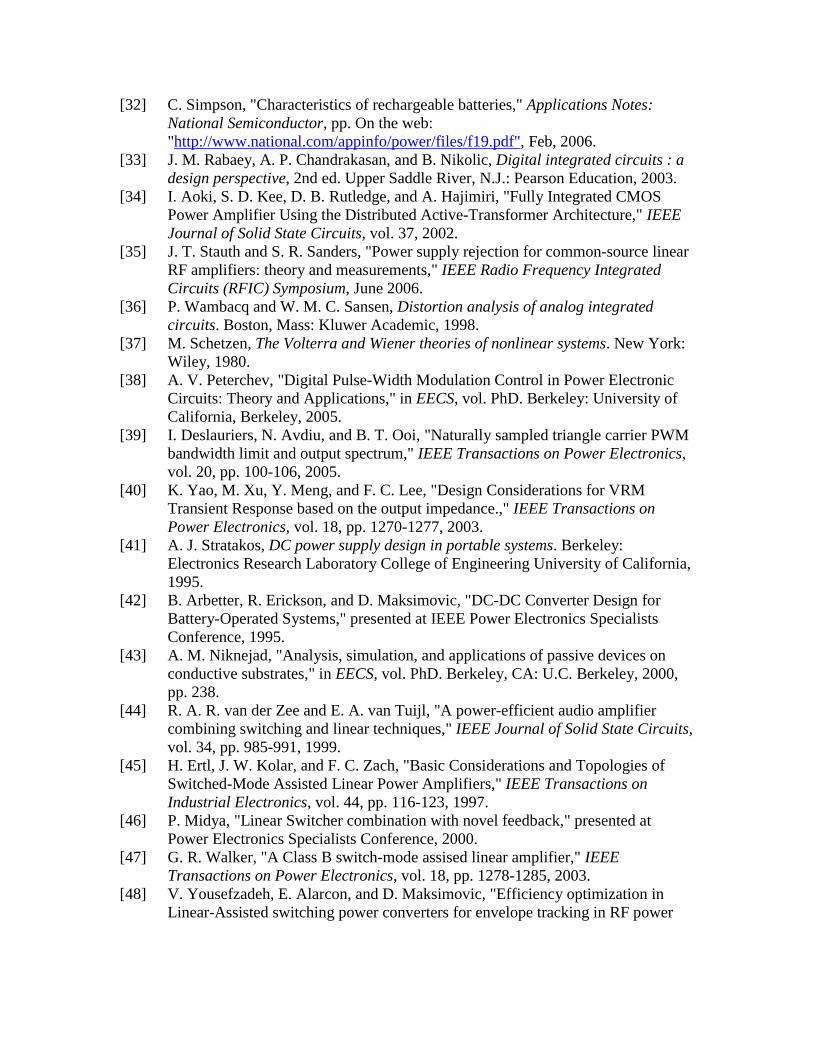
[32] C. Simpson, "Characteristics of rechargeable batteries," Applications Notes: National Semiconductor, pp. On the web: "http://www.national.com/appinfo/power/files/f19.pdf", Feb, 2006.
[33] J. M. Rabaey, A. P. Chandrakasan, and B. Nikolic, Digital integrated circuits : a design perspective, 2nd ed. Upper Saddle River, N.J.: Pearson Education, 2003.
[34] I. Aoki, S. D. Kee, D. B. Rutledge, and A. Hajimiri, "Fully Integrated CMOS Power Amplifier Using the Distributed Active-Transformer Architecture," IEEE Journal of Solid State Circuits, vol. 37, 2002.
[35] J. T. Stauth and S. R. Sanders, "Power supply rejection for common-source linear RF amplifiers: theory and measurements," IEEE Radio Frequency Integrated Circuits (RFIC) Symposium, June 2006.
[36] P. Wambacq and W. M. C. Sansen, Distortion analysis of analog integrated circuits. Boston, Mass: Kluwer Academic, 1998.
[37] M. Schetzen, The Volterra and Wiener theories of nonlinear systems. New York: Wiley, 1980.
[38] A. V. Peterchev, "Digital Pulse-Width Modulation Control in Power Electronic Circuits: Theory and Applications," in EECS, vol. PhD. Berkeley: University of California, Berkeley, 2005.
[39] I. Deslauriers, N. Avdiu, and B. T. Ooi, "Naturally sampled triangle carrier PWM bandwidth limit and output spectrum," IEEE Transactions on Power Electronics, vol. 20, pp. 100-106, 2005.
[40] K. Yao, M. Xu, Y. Meng, and F. C. Lee, "Design Considerations for VRM Transient Response based on the output impedance.," IEEE Transactions on Power Electronics, vol. 18, pp. 1270-1277, 2003.
[41] A. J. Stratakos, DC power supply design in portable systems. Berkeley: Electronics Research Laboratory College of Engineering University of California, 1995.
[42] B. Arbetter, R. Erickson, and D. Maksimovic, "DC-DC Converter Design for Battery-Operated Systems," presented at IEEE Power Electronics Specialists Conference, 1995.
[43] A. M. Niknejad, "Analysis, simulation, and applications of passive devices on conductive substrates," in EECS, vol. PhD. Berkeley, CA: U.C. Berkeley, 2000, pp. 238.
[44] R. A. R. van der Zee and E. A. van Tuijl, "A power-efficient audio amplifier combining switching and linear techniques," IEEE Journal of Solid State Circuits, vol. 34, pp. 985-991, 1999.
[45] H. Ertl, J. W. Kolar, and F. C. Zach, "Basic Considerations and Topologies of Switched-Mode Assisted Linear Power Amplifiers," IEEE Transactions on Industrial Electronics, vol. 44, pp. 116-123, 1997.
[46] P. Midya, "Linear Switcher combination with novel feedback," presented at Power Electronics Specialists Conference, 2000.
[47] G. R. Walker, "A Class B switch-mode assised linear amplifier," IEEE Transactions on Power Electronics, vol. 18, pp. 1278-1285, 2003.
[48] V. Yousefzadeh, E. Alarcon, and D. Maksimovic, "Efficiency optimization in Linear-Assisted switching power converters for envelope tracking in RF power

amplifiers," IEEE International Symposium on Circuits and Systems (ISCAS), pp. 1302-1305, 2005.
[49] J. Phinney and D. Perreault, "Filters with active tuning for power applications," IEEE Transactions on Power Electronics, vol. 18, pp. 636-647, 2003.
[50] H. Kobayashi and P. Asbeck, "Active Cancellation of Switching Noise for DC-DC Converter-Driven RF Power Amplifiers," Microwave Symposium Digest MTT-S, vol. 3, pp. 1647-1650, 2002.