Embed Size (px)
Citation preview

DYNAMIC COMPENSATION OF ELECTRICAL POWER SYSTEMS USING A NEW BVSI
STATCOM
Krishnat V. Patii Department of Electrical & Cornputer Engineering
Faculty of Engineering Science
Graduate Program
in
Engineering Science
I /
Submitted in partial fulfilment
of the requirements for the degree of
Doctor of Philosophy
Faculty of Graduate Studies
The University of Western Ontario
London, Ontario
March 1999
@ Krishnat V. Patil 1999

National Library 1*1 of Canada Bibliothèque nationale du Canada
Acquisitions and Acquisitions et Bibliographie Services services bibliographiques
395 Wellington Street 395. rue Wellington Ottawa ON KIA ON4 Ottawa ON K I A ON4 Canada Canada
The author has granted a non- L'auteur a accordé une licence non exclusive licence allowing the exclusive permettant à la National Library of Canada to Bibliothèque nationale du Canada de reproduce, loan, distribute or sell reproduire, prêter, distribuer ou copies of this thesis in microform, vendre des copies de cette thèse sous paper or electronic formats. la fome de microfiche/^ de
reproduction sur papier ou sur format électronique.
The author retains ownership of the L'auteur conserve la propriété du copyright in this thesis. Neither the droit d'auteur qui protège cette thèse. thesis nor substantial extracts h m it Ni la thèse ni des extraits substantiels may be printed or othekse de celle-ci ne doivent être imprimés reproduced without the author's ou autrement reproduits sans son permission. autorisation.

Abstract and Keywords The cornpetition, cost, and custorner choice are becoming the facets in which soon
to be deregulated and unbundled electrical energy utilities would be working. The
utility companies would need to meet the growing demand of electrical power in
an open transmission access scenario with minimal environmental impact. The fast
acting power electronic converters with their equally fast and efficient controllers are
becoming the backbone of such modern, highly integrated power systems. These
converters give precise and flexible control to an electric power system. A number of
power electronics devices have been proposed for dynamic compensation, improving
system stability, directing power flows, etc. One of the power electronic devices used
for reactive power compensation is a voltage source inverter (VSI). Such an inverter
when connected in shunt with a power system is referred to as a static synchronous
compensator.
This thesis deals with the study of dynamic compensation of electric power systems
using the static synchronous compensator (STATCOM). A new multilevel binary
voltage source inverter (BVSI) which is modular in structure and introduces minimum
harmonics into the system has been proposed to build the ST-4TCOM configuration.
Initially, the application of STATCOM for the damping of torsional oscillations
that occur in a series compensated ac system is examined. The IEEE first bench-
mark system is considered for this study. A STA4TCOM with PI controller is em-
ployed at the generator terminal to regulate its terminal voltage. This PI controller
is augmented with an auxiliary signal derived From the generator speed deviations to
suppress unstable torsional mode oscillations. Eigenvalue analysis is used for small
signal stability evaluation, and optimization of the control systern parameters is done
through step response studies. In addition, dynamic performance of the nonlinear
system with an optimized STATCOM controller is evaluated for a three-phase fault
condition. The results fiom the analytical and digital simulation studies reveal the
technical feasibility of augmenting STATCOM usage for damping of turbine-generator
torsional oscillations in series compensated ac systems.
The use of discretely switched power electronic devices results in contamination
of electrical supply due to harmonics. Hence, care should be taken to minirnize the

introduction of such distortions. A new multilevel binary voltage source inverter
(BVSI) with separate dc sources is introduced. The dc source voltages are staggered
and controlled in binary proportion of &, SI&, 4ViC etc., where PiC is chosen to
get the desired ac voltage output. This n-level BVSI produces a (2"+' - 1)-steps ac
voltage output with n full bridge inverters connected in series. The selective harmonic
elimination modulation technique is used to either completely eliminate or minimize
the harrnonics. -4 closed-loop controller is developed to control the capacitor voltages
and adjust the inverter reactive power output. Application of such a compensator for
dynamic compensation of 13.8 kV distribution system is examined through transient
studies. This inverter c m generate almost sinusoidal output wavefonn, reducing its
harmonic content while ernploying the least number of components and providing a
modular structure.
A laboratory prototype of 400 vars, 120 V, 1-a, 3-level, 15-steps binary voltage
source inverter is implemented for real time tests. A digital controller using Siemens
SAB 80C537 8-bit rnicrocontroller is developed for t his prototype.
The results from digital simulation and hardware irnpiementation show the ef-
fectiveness of BVSI STATCOM as a dynamic compensator under a wide range of
steady state and abnormal operating conditions. The low total harmonic distort ion
validates the effectiveness of the BVSI structure and selected harrnonic elimination
algorithm in minimizing or eliminating harrnonics introduced into the system. The
BVSI STATCOM can smoothly switch the operating mode from leading to lagging
and vice versa without jeopardizing its dynamic performance, steady state behavior,
and harmonic containing capability. The capacitor voltage controller regulates the
capacitor voltages in binary proportion.
The prototype implementation and digital simulation results prove that the com-
pact and modular, precise and fast, flexible and controllable BVSI STATCOM can
deterministically work as reactive power compensator to irnprove the dynamic per-
formance of power systems with minimum power quality degradation.
Keywords Dynamic compensation of power systems
Torsional oscillations
STATCOM Voltage source inverter
Binary voltage source inverter

Co- Aut horship
The following thesis contains material from previously published manuscripts or
manuscripts submitted for publication co-authored by Krishnat V. Patil, R.M. illathur,
J. Jiang, J. Senthil, S.H. Hosseini, and J.E. Makaran.
,411 the research, developmental, simulation and experimental work presented in
this thesis was performed by Krishnat V. Patil. Original rnanuscripts, versions of
which appear in Chapters 2-5 of this thesis, were written by Krishnat V. Patil.

Let noble thoughts and wirdorn corne to us from all quarters.
Rigveda
I-89-i

To
My beloved mother, Indu
vii

Acknowledgement s
-2 thesis is seldom the achievement of an individual. In completing mine, 1 had the
help and support of the following individuals. My heartfelt thanks to al1 of t hem.
Prof. R.M. Mathur for being my technical guru, sharing his unique power system
insights, teaching me how much fun it is to play with voltages and currents in the
pursuit of becoming a practical engineer, making available the needed funds to carry
out my experiments, and letting me learn what it takes to become a nice person.
Prof. Jin Jiang for being a wonderhl supervisor, granting me the freedom of work,
and making me a better badminton player.
Prof. Rajiv Verma for his love, encouragement, and taking the initiative to Bag off
my journey across the Atlantic.
Dr. Jaypalan Senthil, my closest friend, for elevating my spirits up whenever 1 needed
them rnost, and helping me to get my thesis on right track when it meandered in an
unidentified territory.
Prof. S.H. Hosseini for providing the crucial fillip during the mid-age crisis of this
thesis and teaching me power electronics.
John Makaran for sharing his hardware acumen, power electronics expertise, and
taking those late night trips to the lab even during sub-sub zero temperatures.
Yonghui Xu who always willingly gave his time and shared his subtle hardware skills
whenever 1 needed.
Bob Kettlewell for providing me the necessary equipment's, his continued assistance
at every stage of my project, and unmoving patience while solving some rudirnentary
problems.
Prof. George Knorf and Dave Lund for letting me use the 8051 assembler and compiler
from their lab.
viii

Prof. -4rthur Jutan and Prof. Tom Bonnema for their help and being a sincere
well-wisher.
Sharon Ling and Jacquie Taylor who always cheerfully provided the needed assistance
even when thep were having zillions of things to take care of.
M y PEARL pals Cristina, Mufeed, Prof. Khan, Sin for helping to reduce the strain
of long working hours and stress of studies by keeping the lab environment as lively,
joyous, and entertaining as it ever could be.
Haniza, Mi; Amin, Cam, David and many others for that wonderful, memorable time
together.
rEkha-veNu (for being my logical mentor on many occasions), Mamta-Amit, Madan-
Hasu, Mrs Vasanthi Senthil, Amradha (for watching those wonderful Bollywood flicks
with me), Indira and Hari (for those tasteful fruit punches), -4jay Bhaiya & family,
Dev & family, Ratnali-Prashnat, Vatsla-Saurabh, Sandhya-Narendra, Rajiv Bhaiya
& Bhabhiji, who significantly alleviated the pains of living alone and sharing with me
the joys of a home away from home.
Rahul, Amit, Chandu, Bogdan, Ravish, Mandar, Larman, for their delightful friend-
ship.
Al1 those Desis, who were a integral part of my life in London, for making my days
as memorable as one could possibly hope for.
Nilesh, Prashant, Girish, Bhau, Baboo, Manoj, Praveen, my magnetic friends, and
Dr. Ram Nath & family for rnaintaining that long distance coupling energized and
offerhg helping hand whenever I asked for.
Aai-Tatya, Dada-Vahini, Bapu-Kaki, Sarita-Shantaram and others for their undirnin-
ishing love and fathomless affection.
Savita for being mine.
This thesis was typeset by the author using I4Tm2e.

Contents
Certificate of Examination Abstract and Keywords Co-Authorship Epigraph Dedication Acknowledgement s Table of Contents List of Tables List of Figures List of Appendices
vii viii
xiv
xvii
Chapter 1
MODERN P O m R SYSTEM- REQUIREMENTS 1
1.1 THE NATURE OF THE PROBLEM . . . . . . . . . . . . . . . . . . 1
1.1.1 Optimizationofsteady StatePower Flow . . . . . . . . . . . 2
1.1.2 Reactive Power Management . . . . . . . . . . . . . . . . . . . 3 1.1 -3 Damping of Power Oscillations . . . . . . . . . . . . . . . . . 3
1.2 DEREGULATION OF THE ELECTRICAL ENERGY INDUSTRY . 4
1.3 HIGH POWER ELECTRONICS - THE FUTURE . . . . . . . . . . 4
1.4 MEETING A CRITICAL NEED . . . . . . . . . . . . . . . . . . . . 5
1.5 ST-4TIC SYNCHRONOUS COMPENSATOR . . . . . . . . . . . . . 6
1.5.1 V-1 Characteristic of ST-4TCOM . . . . . . . . . . . . . . . . 9 1.6 POWER QUALITY AND STATCOM . . . . . . . . . . . . . . . . . 12
1.7 SCOPE OF THE THESIS . . . . . . . . . . . . . . . . . . . . . . . . 15
1.8 MAJOR CONTRIBUTIONS OF THE THESIS . . . . . . . . . . . . 15
1.9 OUTLINE OF THE THESIS . . . . . . . . . . . . . . . . . . . . . . 17
Bibliography . . . . . . . . . . . . . . . . . . . . . - . . . . . . . . . . . . 19
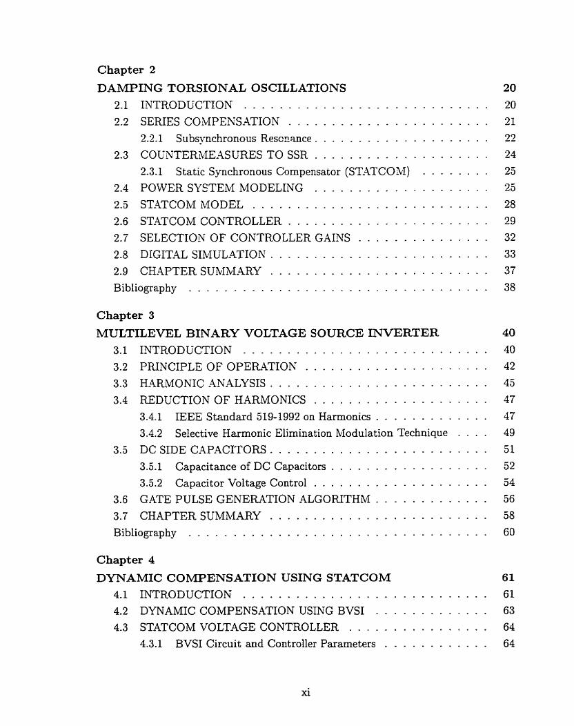
Chapter 2
DAMPING TORSIONAL OSCILLATIONS 20
2.1 INTftODUCTION . . . . . . . . . . . . . . . . . . . . . . . . . . . . 20
2.2 SERIES COMPENS-ATIOR . . . . . . . . . . . . . . . . . . . . . . . 21 vnce . . . . . . . . . . . 3.2.1 Su bsynchronous R e s c
2.3 COUNTERME.4 SURES TO SSR . . . . . . . . . . . 2.3.1 Static Synchronous Compensator (ST.4TCOM)
2.4 POWER SYSTEM MODELING . . . . . . . . . . . 2.5 ST-4TCOM MODEL . . . . . . . . . . . . . . . . . . 2.6 STATCOM CONTROLLER . . . . . . . . . . . . . . 2.7 SELECTION OF CONTROLLER GAINS . . . . . . 2.8 DIGITAL SIkIULATION - - - - - . - - . - - - . - - - 2.9 CH-4PTER SUMM4RY . . . . . . . . . . . . . . . . Bibliography . . . . . . . . . . . . . . . . . . . . . . . . .
Chapter 3
MULTILEVEL BINARY VOLTAGE SOURCE INVERTER 40
. . . . . . . . . . . . . . . . . . . . . . . . . . . . 3.1 INTRODUCTION 40 . . . . . . . . . . . . . . . . . . . . . 3.2 PFUNCIPLE OF OPERATION 42
. . . . . . . . . . . . . . . . . . . . . . . . . 3.3 H-4RMONIC ANALYSIS 45
3.4 REDUCTION OF H-4RMONICS . . . . . . . . . . . . . . . . . . . . 47
3.4.1 IEEE Standard 519-1992 on Harmonics . . . . . . . . . . . . . 47
. . . . 3.4.2 SeLective Harrnonic Elimination Ivfodulation Technique 49 . . . . . . . . . . . . . . . . . . . . . . . . . 3.5 DC SIDE CAPACITORS 51
. . . . . . . . . . . . . . . . . . 3.5.1 Capacitance of DC Capacitors 52 . . . . . . . . . . . . . . . . . . . . 3.5.2 Capacitor Voltage Control 54
. . . . . . . . . . . . . 3.6 GATE PULSE GENERATION ALGORITHM 56 . . . . . . . . . . . . . . . . . . . . . . . . . 3.7 CHAPTER SUMMARY 58
. . . . . . . . . . . . . . . . . . . . . . . . . . . . . . . . . . Bibliography 60
Chapter 4
DYNAMIC COMPENSATION USING STATCOM 61
. . . . . . . . . . . . . . . . . . . . . . . . . . . . 4.1 INTRODUCTIOIL' 61
4.2 DYNAMIC COMPENSATION USING BVSI . . . . . . . . . . . . . 63 . . . . . . . . . . . . . . . . 4.3 STATCOMVOLTAGECONTROLLER 64
4.3.1 BVSI Circuit and Coatroller Parameters . . . . . . . . . . . . 64

4.3.2 Voltage Controller Parameters . . . . . . . . . . . . . . . . . . 65
4.4 TRAXSIEXT SIMULATION . . . . . . . . . . . . . . . . . . . . . . 65
1.4.1 Switching from Leading to Lagging Mode of Operation . . . . 65
. . . . . . . . . 4.4.2 Three-phase to Ground Fault at Load Bus .. 66
. . . 4.43 Three-phase to Ground Fault ivhen ST4TCOM Flûating 67
. . . . . . . . . . . 4.4.4 Single-phase to Ground Fault at Load Bus 61
4.4.5 Line to Line Fault at Load Bus . . . . . . . . . . . . . . . . . 67
4 BVSI -4s SSSC . . . . . . . . . . . . . . . . . . . . . . . . . . . . . . 74
4.6 CHAPTER SUMMARY . . . . . . . . - - - . - - - - - - - - - - - - - 74 CIC Bibliography . . . . . . . . . . . . . . . . . . . . . . . . . . . . . . . . . . i CI
Chapter 5
LABORATORY PROTOTYPING AND EVALUATION OF BVSI 76
5.1 11'4TRODUCTION . . . . . . . . . . . . . . . . . . . . . . . . . . . . 76
2 PROTOTYPE SPECIFICATIONS . . . . . . . . . . . . . . . . . . . 77
5.3 H-4RDW-4RE DESIGN . . . . . . . . . . . . . . . . . . . . . . . . . . 79
5.3.1 3-level, lbsteps, 1 4 BVSI Configuration . . . . . . . . . . . . 81
5.3.2 BVSI Controller . . . . . . . . . . . . . . . . . . . . . . . . . . 82
5.3.3 Gate Pulse Generation . . . . . . . . . . . . . . . . . . . . . . 85
5.3.4 RMS Load Bus Voitage as Input to PI Controller . . . . . . . 86
5.3.5 Synchronizatio~ of Power System and BVSI . . . . . . . . . . 86
5.3.6 +15 V Regulated DC Supply for Gate Drive Circuits . . . . . 88
5.4 CONTROLLER DESIGN . . . . . . . . . . . . . . . . . . . . . . . . 88
5.4.1 Voltage Controller . . . . . . . . . . . . . . . . . . . . . . . . 88
5.4.2 Gate Firing Control . . . . . . . . . . . . . . . . . . . . . . . . 90
5.5 CONTROLLER IMPLEMENTA4TION . . . . . . . . . . . . . . . . . 90
5.5.1 Synchronization . . . . . . . . . . . . . . . . . . . . . . . . . . 91
5.5.2 .4 /D Conversion of RMS Load Bus Voltage . . . . . . . . . . . 92
5.5.3 Digital PI Controller . . . . . . . . . . . . . . . . . . . . . . . 92
. . . . . . . . . . . . . . . . . . . . . . . . 5.5.4 Gate Firing Control 93
5.6 PERFORMANCE VERIFICATION . . . . . . . . . . . . . . . . . . 93
5.6.1 Overview of Study Cases . . . . . . . . . . . . . . .. . . . . . 94
5.6.2 Discussion of Results . . . . . . . . . . . . . . . . . . . . . . . 95 5.7 HARDWAFLELIMITATIONS . . . . . . . . . . . . . . . . . . . . . . 107
5.8 CH-4PTER SUMMARY . . . . . . . . . . . . . . . . . . . . . . . . . 108
Bibliography . . . . . . . . . . . . . . . . . . . . . . . . . . . . . . . . . . 109
xii

Chapter 6
EPILOGUE 110
6.1 CO-iCLUSIONS . . . . . . . . . . . . . . . . . . . . . . . . . . . . . 110 6.2 SUGGESTED FUTURE WORK . . . . . . . . . . . . . . . . . . . . 112
. . . . . . . . . . . . . . . . . . . . . . . . . . . . . . . . . . Bibliography 113
Appendix A
PO-R SYSTEM MODELING 114
A.1 REFERENCE FRAME TRANSFORiLIATION . . . . . . . . . . . . . 114
A.2 MECH-kXIC-AL SYSTEM MODELING . . . . . . . . . . . . . . . . 116 . . . . . . . . . . . . . . . . . . . . . . 4 . 2 1 SLu hlass Rotor Mode1 116
. . . . . . . . . . . . . . . A.2.2 Governor and Steam Turbine Mode1 118 . . . . . . . . . . . . . . A.2.3 State Equation of Mechanical System 118
. . . . . . . . . . . . .4.3 SYNCHRONOUS GENERATOR MODELING 119 . . . . . . . . . . . . . . . . . . . . . A3.1 Rotor Circuit Equations 119 . . . . . . . . . . . . . . . . . . . . . .4.3.2 Stator Voltage Equations 121
. . . . . . . . . . . . . . . . . . . . . . . . . . 4.3.3 Electric Torque 122 . . . . . . . . . A.3.4 Generator Equations on Common R-1 Frame 123
. . . . . . . . . . . . . . . . . *4.4 EXCITATION SYSTEM MODELING 124 A.5 ST-4TCOM CIRCUIT, CONTROLLER MODELING . . . . . . . . . 123
. . . . . . . . . . . . . A.5.l STATCOM Circuit AC Side Equations 125
. . . . . . . . . . . . . A.5.2 STA4TCOh.I Circuit DC Side Equations 126 . . . . . . . . . . . . . . . . A.5.3 STATCOM ControlIer Equations 128
A.6 TR4NSblISSION NETWORK MODELING . . . . . . . . . . . . . . 130
.4.7 SMALL SIGNAL MODEL OF COMPLETE SYSTEM . . . . . . . . 131
Appendix B
GATE PULSE GENERATION 136
. . . . . . . . . . . . . . . . . . . . . . . . . . . . . . B.l GATE PULSES 136
Appendix C
IEEE COPYRIGHT TRANSFER FOR CHAPTER 2
Appendix D
IEEE COPYRIGHT TRANSFER FOR CHAPTERS 3. 4
Vita
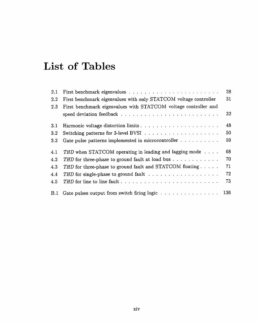
List of Tables
. . . . . . . . . . . . . . . . . . . . . . . 2.1 First benchmark eigenvalues 28
2.2 First benchmark eigenvalues with only STATCOM voltage controller 31
2.3 First benchmark eigenvalues mith ST.4TCOM voltage controller and
. . . . . . . . . . . . . . . . . . . . . . . . . speed deviation feedback 32
. . . . . . . . . . . . . . . . . . . . 3.1 Harrnonic voltage distortion limits 48
. . . . . . . . . . . . . . . . . . . 3.2 Smitching patterns for 3-level EVSI 50
. . . . . . . . . . 3.3 Gate pulse patterns implemented in rnicrocontroller 39
. . . . 4.1 THD when STATCOM operating in leading and lagging mode 68
. . . . . . . . . . . . 4.2 THD for three-phase to ground fault at load bus 70
. . . . . 4.3 THD for three-phase to ground fault and STATCO3f floating 71
. . . . . . . . . . . . . . . . . . 4.4 THD for single-phase to ground fault 72
. . . . . . . . . . . . . . . . . . . . . . . . . 4.5 THD for line to line fault 13
. . . . . . . . . . . . . . . B . 1 Gate pulses output from switch firing logic 136
xiv

List of Figures
Elernentan; six-pulse voltage source inverter SIXTCOM . . . . . . . 7
V-1 characteristic of ST-4TCOM . . . . . . . . . . . . . . . . . . . . . 10
. . . . . . . . Power exchange between the STATCOM and ac system Il
.4 C line voltage output of a six-pulse voltage source inverter For 180"
. . . . . . . . . . . . . . . . . . . . . . . . . . . conduction sequence 13 Output voltage of a 48-pulse STATCOM generating reactive power . 14
Network for SSR darnping studies and six mass rotor mode1 . . . . . SSR modes of first benchmark mode1 . . . . . . . . . . . . . . . . . . Steady state characteristics of STATCOM . . . . . . . . . . . . . . .
. . . . . . . . . . . . . . . . . . . . . . . . . . . STA4TCOM controller
. . . . . . . . . . . 10 % step change in Kef for 72.25% compensation
Simulation results with only ST.4TCOM voltage controller for 72.25%
. . . . . . . . . . . . . . . . . . . . . . . . . . . . . . . compensation
Simulation results with ST.4TCOM voltage controller and speed devi-
ation feedback for 72.25% compensation . . . . . . . . . . . . . . . . LPB-GEN shaft torques for other critical compensation levels with
. . . . . . ST-ATCOM voltage controller and speed deviation feedback
. . . . . . . . . . . . . . . . Three-phase star connected 3-level BVSI 43
. . . . . . . . . . . . . . . . . . . . . Typical voltages of 3-level BVSI 44
. . . . . . . . . . . . . . . . . Modulation angles derived from SHEM 51
Modulating charge and discharge of capacitors to control their voltages 54
. . . . . . . . . . . . . . . . . . . . . . . Capacitor voltage controller 56 . . . . . . . . . . . . . . . . . . . . . . . . . . . . Gate pulse patterns 57
Distribution system compensation using BVSI . . . . . . . . . . . . . 63
. . . . . . . . . . . . . . . . Addition of capacitive and inductive load 68
. . . . . . . . . . . . . . Typical STATCOM real power consumption 69
1.4 Three-phase to ground fault . . . . . . . . . . . . . . . . . . . . . . . 70
. . . . . . . . 4.5 Three-phase to ground fault when STATCOM floating 71
. . . . . . . . . . . . . . . . . . . . . . . 4.6 Single-phase to ground fault 72
. . . . . . . . . . . . . . . . . . . . . . . . . . . . . 4.7 Line to iine fault 73
5.1 Picture of the BVSI Prototype . . . . . . . . . . . . . . . . . . . . . . 78
5.2 Laboratory power system setup . . . . . . . . . . . . . . . . . . . . . 79
5.3 Complete hardware configuration . . . . . . . . . . . . . . . . . . . . 80
5.4 MO0 vars, 120 V: 14 , 34evel. 15-steps Binary VSI . . . . . . . . . . 81
5.5 FBI using POWEREX's PMlJCSJ060 Intelligent Module . . . . . . . 83
. . . . . . . . . . . . . . . . . . . 5 SAB 80C53'7 microprocessor circuit 84
5.7 Firing pulse generation from microcontroller output . . . . . . . . . . 85
5.8 RMS voltage measurement using AD637JQ . . . . . . . . . . . . . . . 87
5.9 Zero crossing detector . . . . . . . . . . . . . . . . . . . . . . . . . . 87
5.10 Regulated t l 5 V dc supply . . . . . . . . . . . . . . . . . . . . . . . 88
5.1 1 Typical gate pulse patterns . . . . . . . . . . . . . . . . . . . . . . . . 90
. . . . . . . . . . . . . . . . . . . . . . . . . . 5.12 Synchronization signal 91
5.13 Simulation setup . . . . . . . . . . . . . . . . . . . . . . . . . . . . . 94
. . . . . . . . . . . . . . . 5.14 Case 1- BVSI floating, switching in R load 97
. . . . . . . . . . . . . . . 5.13 Case 2- BVSI floating, switching in L load 98
. . . . . . . . . . . . . . . 5 . E Case 3- BVSI floating, switching in C load 99
. . . . . . . . . . . . . . 5.17 Case 4- BVSI floating, switching in RL loads 100
. . . . . . . . . . . . . . 5.18 Case 5- BVSI floating, switching in RC loads 101
. . . . . . . . . . . . . . 5.19 Case 6- BVSI fioating, switching in LC loads 102
. . . . . . . . . . . . . 5.20 Case 7- BVSI floating, switching in RLC loads 103
5.21 Case 8- BVSI, R/L loads connected, switching in R/L/C loads . . . . 104
5.22 Case 9- BVSI, RL/RC/LC hads connected, switching out R/L/C loads 105
5.23 Case 10- BVSI, RLC loads connected, switching out R/L/C loads . . 106
. . . . . . . . . . . . . . . . . . . . . -4.1 Reference frame transformation 115 . . . . . . . . . . . . . . . . . . . . . . . . . . . . -4.2 Mechanical system 117
. . . . . . . . . . . . . . . . . A.3 Synchronous machine equivalent circuit 119 . . . . . . . . . . . . . . . . A.4 Synchronous generator excitation system 124
. . . . . . . . . . . . . . . . . . . . . . . . . . . . A.5 STATCOM circuit 125
. . . . . . . . . . . . . . . . . . . . . . . . . . . A.6 STATCOM controller 128
. . . . . . . . . . . . . . . . . . . . . . . . . . . A.? Transmission network 130
xvi
List of Appendices
A POTVER SYSTEM MODELING . . . . . . . . . . . . . . . . . . . . 114
B GATE PULSE GENERATION - . . . . . . . . . . . . . . . . . - . . 136
C IEEE COPYRIGHT TR4NSFER FOR CH-4PTER 2 . . . . . . . . . 139
D IEEE COPYRIGHT TRANSFER FOR CH-4PTERS 3: 4 . . . . . . . 140
xvii

Chapter 1
MODERN POWER SYSTEM- REQUIREMENTS
1.1 THE NATURE OF THE PROBLEM
The electric utility companies are faced with growing demand of electrical energy,
and simultaneously ensuring reliability of an electrical supply. The modern electrical
power system grid has become a highly integrated transmission network comprising
many synchronous generators, ac lines, dc lines, passive and active loads, and nu-
merous controllers. For example, the power system network of Ontario Hydrol is
an integrated system of more than 29,000 kilometers of high-voltage transmission
lines, towers and transformer stations across Ontario, with interconnections to elec-
tricity grids in neighboring provinces and states serving more than 300 municipal
electric utilities, and direct industrial customers in Ontario. This network also pro-
vides telecommunication links for major cellular phone systems serving Ontario. Such
an integrated network while bearing many advantages also suffers because it experi-
ences voltage and power excursions caused by events such as sudden load changes,
faults, and controller actions taking place locally and/or remotely.
The utilities need to deliver electric power with minimal environmental
New additions to electrical power transmission networks do not take place
impact.
without
1.1. THE NATURE OF THE PROBLEM 2
being subjected to critical environmental and regulatory clearance and full economic
justification. Instead, the increased transmission demand is met where possible by
increasing the existing transmission capacity. When trying to improve the transmis-
sion capacity, a key assumption is made that if the overall system reliability is not
irnproved, at Ieast the existing system reliability is rnaintained. Systern reliability has
two important aspects: adequacy and security. Adequacy is defined as the ability of
the power system to meet the energy demands, within cornponent ratings and voltage
Iimits. Security is referred to as the ability of the power system to withstand inci-
dents (faults or equipment outages) without uncontrolled l o s of customer load. At
issue is the value of the efforts and expenses to make more efficient use of the existing
transmission systems (more adequacy), without endangering system security.
A variety of nenr devices with their appropriate controllers are added in a power
system to exploit under-utilized thermal capacities of the existing ac transmission
lines. The objectives of adding new devices are to change the impedance of trans-
mission lines, regulate the network bus voltages, and control load angles. These
parameters are controlled either independently or simultaneously. The choice of a
control device depends upon the system requirements as described in the following
sections.
1.1.1 Optimization of Steady State Power Flow
Increasing power flow, while maintaining security and reliability, maximizes the gains
from power delivery infrastructure, one of the most valuable assets in the competitive
business environment. For a power system, the goal is to operate it with a power flow
that takes all relevant security constraints into account, uses minimum capacity and
incurs minimum transmission losses. Running the system close to minimum losses is
one of the most important operating targets for a competitive power system. It is
atternpted to keep the system in a safe and near-optimum state under varying loads
and generating conditions. However, the optimum network configuration changes
1.1. THE NATURE OF THE PROBLEM 3
from time to tirne due to technical, operational, iegal and economical reasons. The
configuration of the surrounding network changes, loading changes and the opportu-
nities for energy trading Vary. There is certain incentive for increasing the flexibility
of the transmission system for t hese reasons.
1.1.2 Reactive Power Management
Reactive power is generated by lightly Ioaded ac transmission lines and absorbed by
heavily loaded lines, transformers and most of industry loads. This is an essential
feature of the operation of an ac network, but it interferes with the efficient trans-
mission of real power. The hvdc systems solve this problem by removing al1 reactive
power frorn the lines and dealing with it at the terrninals. A less drastic solution is to
control the reactive power itself. The synchronous generator escitation, transformer
tap-changing, Iine switching and synchronous compensators influence reactive power
fiow. If rapid control of vars is available, the quality of the power supply improves
considerably by very fast and accurate adjustment of reactive power.
1.1.3 Damping o f Power Oscillations
One aspect of large ac systern development is the transmission of bulk power from
remote sources to load centers over long distance transmission s ystems operating
a t the highest voltage Ievels. When a long, weak line connects two big networks
electromechanical oscillations, power oscilZatzons, may occur whenever power floiv on
the line changes. The oscillations rnay also be created by transient line faults and
after clearing such faults. -4 poor damping of these oscillations can be a decisive factor
in limiting the amount of power that c m be transmitted over a transmission network.
The typical stable loadability of long transmission lines, is therefore mostly about 113
of their thermal transmission limit. This limit c m be raised by improving the line
damping. Sraditionally transmission oscillations are eliminated by the use of power
system stabilizers (PSS) added to the generator excitation systerns. However, when
1.2. DEREGULATION OF T m ELECTRICAL ENERGY INDUSTRY 4
the oscillation frequency is very low (0.7 to 2 Hz) such as in inter area oscillations,
the PSS become ineffective. Under these circumstances fast controllable devices are
required, which possess fast line power flow control capaciY.
1.2 DEREGULATION OF THE ELECTRICAL ENERGY INDUSTRY
Besides the above stated technical reasons: there is a trend to open up the electrical
energy markets. Worldwide, in numerous countries the deregulation of t heir electric
power industry is imminent and in some places, eg., United Kingdom, California, the
energy markets are already deregulated. -4s the electric power industry undergoes its
most fundamental transition in a century, many of the forces of change are converg-
ing upon power delivery systems. The deregulation is going to increase cornpetition
arnong utilities and bring new participants into electricity markets - necessitating
more flexible, more controllable and more adaptive transmission and distribution
networks in order to cope. In this new era, electric utilities will be transformed and
advanced technologies will play an important role in providing cornpetit ive advantage
and in meeting the challenges ahead. The utilities that will prosper in this nerv era
of market growth and change will be those that can realize strategic advantage from
emerging technological opportunities. Flexible AC Transmission System (FACTS) [l]
devices and other complementary technologies can minimize costly capital invest-
ments, but evaluating and selecting the appropriate devices is a complex task. Power
system planners need a way to identify the optimal FACTS solution for maximizing
system capabilities.
1.3 HIGH POWER ELECTRONICS - THE FUTURE
Advanced high power electronics promise revolutionary increases in the performance,
flexibility, and cost-effectiveness of electricity transmission, distribution, and end-use.
1.4. MEETING A CRTTICAL NEED 5
These improvements will help electricity providers adapt to and exploit tomorrow's
deregulated, cornpetitive power markets.
Power electronic technologies are analogous to low power transistors and inte-
grated circuits but operational a t multi megawatt power lewls. As such, they offer
durable solid-state devices in the place of clumsy, wear-prone mechanical switches
and systems currently ernployed for control of transmission and distribution networks.
These electronics enable full realization of F.I\CTS and Custom Power [2] technologies,
with the potential for optimum tuning and precise control of al1 power circuits.
High power electronic devices are bringing unprecedented increases in efficiency
and cost-effectiveness in electrical power systems. Moreover, the operational flexibility
t hey introduce will enable utilities to significantly increase asset ut ilizat ion and deliver
new value-added customer services.
MEETING A CRITIC AL NEED
Recent technological advancernents in the area of power elect ronics, rnicroprocessors,
microelectronics, digital signal processors and communications have been used to de-
vise neur means to make the power system more reliable, more controllable and more
efficient. The use of fast acting power electronic converters with their equally fast and
efficient controllers give a precise and flexible control of an electrical power system.
An inverter, which converts dc voltage into a single or polyphase ac voltage of a de-
sired amplitude and frequency, is the most visible among the various power electronic
devices employed in power systems. Today it is possible to manufacture semiconduc-
tor devices having a thermal and surge current handling capability that correspond
well t o normal voltage and current rating of high power lines and associated short
circuit currents. Conventional thyristors cannot be turned-off until there is a natural
current zero or one is artificially created for forced commutation. On the contrary,
simpler turn-off capabilities of self cornmut ating devices like gate turn-off thyristors

1.5. STATIC SYNCHRONOUS COMPENSATOR 6
(GTO) , insulated-gate bipolar transistors (IGBT) , insulated-gate controlled t hyris-
tors (IGCT) have given a new dimension to inverter applications in power systems.
-4 relatively recent concept, FACTS stems from the fact that self comrnutating, high
voltage, high current and high switching frequency ponrer electronic devices can be
used to produce subsystems which make the operation of ac transmission highly con-
trollable and therefore flexible. F4CTS have revolutionized the world of electrical
power systems.
Since the concept of F-CTS was introduced. a family of power electronics equip-
ment has emerged for controlling and optimizing the performance of power sys-
tems. The family of equipment includes the static synchronous compensator (ST-4T-
COM) [3], the static synchronous series cornpensator (SSSC) [4], and the unified
power flow controller (UPFC) [5]. The theoretical capabilities of these FACTS de-
vices have been described in [3, 4, 51 as well as in many other papers. These devices
have been the subject of extensive study and discussion in recent times. The prac-
tical viability of this technology has also been demonstrated by the recent successful
commissioning of the HO0 MVAR ST.4TCOM project [6] for the Tennessee Valley
Authority, the first such installation in the world. A second major project is already
undenvay to install first large scale UPFC for American Electric Power (71.
In this thesis, STATCOM applications in power system are investigated through
digital simulation and laboratory prototype studies.
1.5 STATIC SYNCHRONOUS COMPENSATOR
A static synchronous compensator (STATCOM or SSC) is a shunt connected reactive
power compensation device which is capable of generating and/or absorbing reactive
power whose output c m be varied to control specific parameters of an electric power
system. It is, in general, a solid-state switching converter, capable of generating or
absorbing independently controllable real and reactive power a t its output terminais,

1.5. STATIC SYNCHRONOUS COMPENSATOR 7
when it is fed from an energy source or an energ'. storage device at its input terminais.
Specifically, the STATCOM considered in t his t hesis is a voltage source inverter t hat
produces from a given input dc voltage a set of three-phase ac output voltages, each
of which is in phase 114th: and coupled to the corresponding ac system voltage via a
relatively small reactance (mhich is provided either by an interface reactor or leakage
inductance of a coupling transformer). The cic voltage is provided by an energy
storage capacitor.
The ST.4TCOM is analogous to an ideal synchronous machine which generates a
balanced set of t hree sinusoidal voltages, at the fundament al frequency, wit h con-
trollable amplitude and phase angle. This ideal machine has no inertia, its re-
sponse is practically instantaneous, it does not significantly alter the esisting system
impedance, and it can internally generate reactive (both capacitive and inductive)
p ower [3].
An elementary six-pulse voltage source inverter STATCOM is shown in Figure 1.1.
A six-pulse voltage source inverter consists of six self commutated semiconductor
sntitches (IGBT or GTO) with antiparallel diodes. With a dc voltage source (which
may be a charged capacitor), the inverter can produce a balanced set of three quasi-
Figure 1.1: Elementary six-pulse voltage source inverter STATCOM
1.5. STATIC SYNCHRONOUS COMPENSATOR 8
square voltage waveforms of a given frequency by connecting the dc source sequentially
to the three output terminals via the appropriate inverter switches.
The reactive power exchange between the inverter and the ac system can be con-
trolled by vaqing the amplitude of the three-phase output voltage, V,, of the inverter.
That is, if the amplitude of the output voltage is increased above that of the utility
bus voltage, G, then the current flows through the reactance from the inverter to the
ac system, and the inverter generates capacitive reactive power for the ac system.
If the amplitude of the output voltage is decreased belom the utility bus voltage,
then the current flows from the ac system to the inverter, and the inverter absorbs
inductive reactive power from the ac system. If the output voltage is equal fo the ac
system voltage, the reactive power exchange is zero, and the STATCOM is said to be
in a floating state.
Similarly, the real power exchange betrveen the inverter and the ac system can be
controlled by adjusting the phase shift between the inverter output voltage and the ac
system voltage. That is, the inverter can supply real power to the ac systern from its
dc energy storage if the inverter output voltage is made to lead the ac system voltage.
On the other hand, it can absorb real power from the ac system for dc energy if its
voltage lags the ac system voltage.
The STATCOM provides the desired ieactive power by exchanging the instanta-
neous reactive power arnong the phases of the ac system. The mechanism by which
the inverter internally generates and/or absorbs the reactive power can be understood
by considering the relationship between the output and input powers of the inverter.
The inverter switches connect the dc input circuit directly to the ac output circriit.
So the net instantaneous power a t the ac output terminals must always be equal to
the net instantaneous power at the dc input terminals (neglecting losses) [3].
Assume that the inverter is operated to supply only reactive output power. In
this case, the real power provided by the dc source as input to the inverter h a to be
f -5. STATIC SYNCWRONOUS COMFENSATOR 9
zero. Furthermore, since reactive power at zero frequency (dc) by definition is zero,
the dc source supplies no reactive power as input to the inverter. Thus it clearly plays
no part in the generation of reactive output pomer by the inverter. In other words:
the inverter simply interconnects the three output terminals in such a way that the
reactive output currents can flow freely among them. Viewing this from the terminals
of the ac system, it means that the inverter establishes a circulating reactive power
exchange among the phases. On the other hand, the real power that the inverter
exchanges a t its ac teminals -4th the ac system must, of course, be supplied to, or
absorbed from, its dc terminals by the dc capacitor.
-4lthough reactive power is internally generated by the action of inverter switches,
it is still necessary to have a dc capacitor connected across the input terminals of
the inverter. The need for the capacitor is primarily to provide a circulating current
path as well as a voltage source. The magnitude of the capacitor is not important,
but generally it is chosen such that the dc voltage across its terminais remains fairly
constant so that it doesn't contribute to the ripples in the dc current. The inverter
output voltage is a stair case wave whereas it draws smooth sinusoidal current from
the ac system. This results in slight fluctuations in the output power of the inverter.
However, in order not to violate the instantaneous power equality constraint a t its
input and output terrninals, the inverter must draw a fluctuating current from its
dc source. Depending upon the inverter configuration employed, it is possible to
calculate the minimum capacitance required to meet the system requirements such
as ripple limits on the dc voltage and the rated reactive power support needed by the
ac system.
1.5.1 V-1 Characteristic of STATCOM
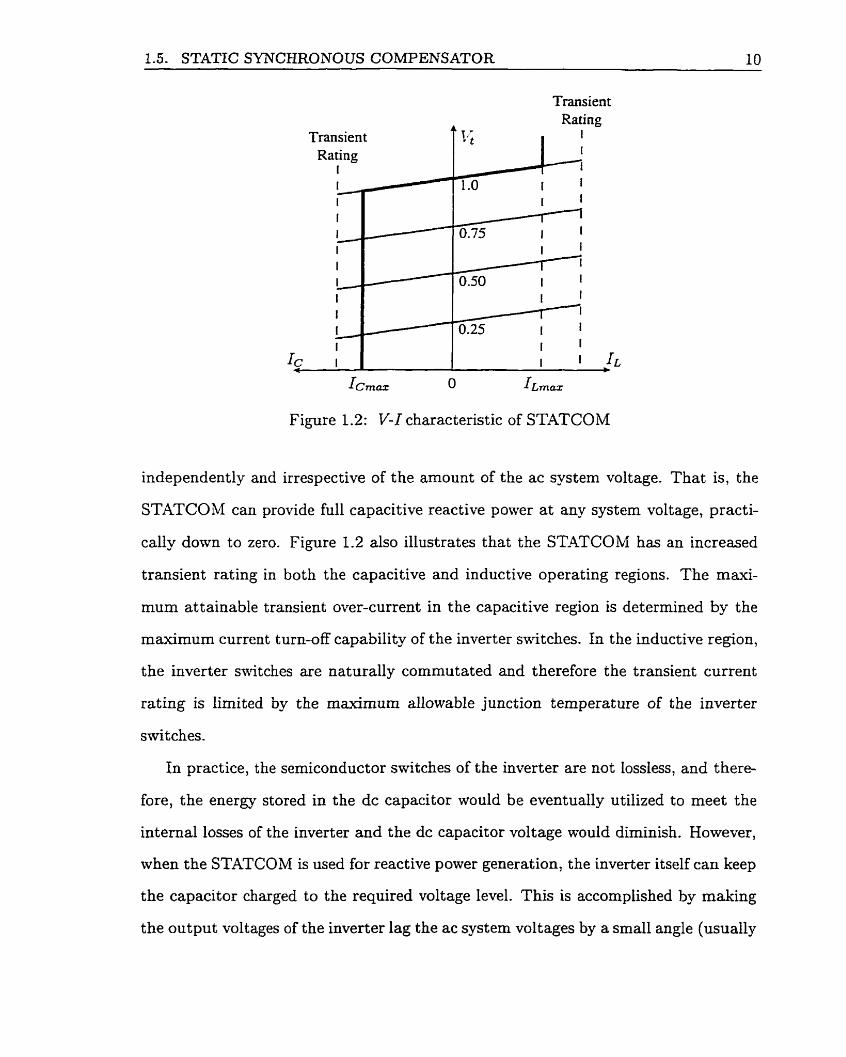
A typical V-I charactenstic of STATCOM is depicted in Figure 1.2. As can be seen,
the STATCOM can supply both capacitive and inductive compensation and is able
to control its output current over the rated maximum capacitive or inductive range
1.5. STATIC SYNCHRONOUS COMPENSATOR 10
Figure 1.2: V-1 characteristic of STATCOM
Transient
Transient Rating
independently and irrespective of the amount of the ac system voltage. That is, the
I I I /-75%- I I
I I
STATCOM can provide full capacitive reactive power a t any system voltage, practi-
I I I 1 I 1 I I
/
0.50 I I I I
cally down to zero. Figure 1.2 also illustrates that the ST-4TCOM has an increased
transient rating in both the capacitive and inductive operating regions. The maxi-
I
/ 0.25
mum attainable transient over-current in the capacitive region is determined by the
I I
maximum current turn-off capability of the inverter switches. In the inductive region,
I I I 1 :L
the inverter switches are naturally commutated and therefore the transient current
rating is lirnited by the maximum allowable junction temperature of the inverter
switches.
In practice, the semiconductor switches of the inverter are not Iossless, and there-
fore, the energy stored in the dc capacitor would be eventually utilized to meet the
interna1 losses of the inverter and the dc capacitor voltage would diminish. However,
when the STATCOM is used for reactive power generation, the inverter itself can keep
the capacitor charged to the required voltage level. This is accomplished by making
the output voltages of the inverter lag the ac systern voltages by a small angle (usuaily

1.5. STATIC SYNCHRONOUS COMPENSATOR 11
in the range of 0.1" to 0.2O). In this way the inverter absorbs a small amount of real
power from the ac system to meet its interna1 losses and keep the capacitor voltage
a t the desired Ievel. The same mechanism can be used to increase or decrease the
capacitor voltage, and thereby the amplitude of the output voltage of the inverter,
for the purpose of controlling the var generation or absorption.
The reactive and real power exchange between the STATCOM and the ac sys-
tem can be controlled independently of each other and any combination of real power
generation or absorption nrith var generation or absorption is achievable, if the STAT-
COM is equipped with an energy storage device of suitable capacity, as depicted in
Figure 1.3. With this capability, exfremely eEective control strategies for modula-
tion of the reactive and real output power can be devised to improve transient and
dynamic system stability limits.
AT ,4C TERMINAL f
Kc AC System I
3 Interface Reactor
STATCOM Lx Energy S torage
1 ac absorbs P 1 supplies
- P
Kc
absorbs P supplies P absorbs Q ' absorbs Q
AT DC TERMINAL
absorbs P 1 supplies P
Figure 1.3: Power exchange between the STATCOM and ac system

1.6. POWER QUALITY AND STATCOM 12
1.6 POWER QUALITY AND STATCOM
The power quality involves issues like voltage flicker, voltage dip, voltase rise, har-
monic performance and high frequency noise. Power electronics devices distort voltage
and current waveforms in a power network which have diverse influences on power
facilities and customers' equipment. Harrnonic currents induce abnormal noise and
parasitic losses. Also, harmonic voltages cause loss of accuracy in measurement in-
struments, faulty operation of the relay and control systems. Electromagnetic noise
is caused by the noise of the high frequency electmrnagnetic waves emitted from
power electronic circuits. It affects electronic devices used in business and industry,
and often induces interfering voltage in communication lines. The corrective measure
generally recommended to avoid harrnonics and high frequency noise is to limit their
generation at the source. In this thesis the discussion of harrnonics generation and
its control is limited to ST-4TCOM.
In principle, the STATCOM output voltage wave is a staircase type wave syn-
thesized from dc input voltage with appropriate combinations of inverter switches.
For example, the six-pulse inverter shown in Figure 1.1 is typically operated with
either 120" or 180" conduction sequence for inverter switches. For 180" conduction
sequence, three switches conduct at a time and for 120" conduction sequence, two
switches conduct at a time. Figure 1.4 shows the 3-steps staircase line voltage, uab,
for a conduction sequence of 180". The line voltage uab in terms of its various fre-
quency components can be described by the following Fourier series.
where coefficients a,, ah, and bh can be determined considering one fundamental
period of U a b The v.b waveform is symmetrical, so the average voltage a, = O. It also

1.6. POWER QUALITY AND STATCOM 13
Figure 1.4: .4C line voltage output of a six-pulse voltage source inverter for 180" conduction sequence
has odd wave symmetry, so ah = O. The coefficient bh is determined as
- - cos(hcr) - cos h ( ~ - 7rh

1.6. POWER QUALITY AND STATCOM 14
Therefore,
For 180" conduction sequence, a = 30°, so (1.3) shows that the triple harrnonics
are zero in the line voltage. From (1.3), it can also be seen that the inverter bas
harmonic components of frequencies (6k f 1) f, in its output voltage and 6k f, in its
input current, where f, is the fundamental output frequency and k = 1 .2 ,3 : . . . . As
is evident, the high harmonic content in the output voltage rnakes this simple inverter
impractical for the power system applications.
To reduce the harmonics generation wrious inverter configurations as well as
inverter switching techniques are suggested in the literature. For exampie, the first
ever commercial STATCOM [6] installed has a 48-pulse inverter configuration so that
the staircase ac line output voltage waveform has 21-steps as shown in Figure 1.5 and
it better approaches an ideal sinusoidal waveform reducing harmonics content. The
switching strategies like selective harmonic elimination techniques also help in limiting
Figure 1.5: Output voltage of a 48-pulse STATCOM generating reactive power

1.7. SCOPE O F THE THESIS 15
the harrnonic generation at the source. In this thesis both inverter configuration and
switching strategy alternatives to limit harrnonic generat ion are studied.
1.7 SCOPE OF THE THESIS
This thesis mainly examines the use of Static Synchronous Cornpensator in an electric
power system to irnprove its performance in wrying operating and physical conditions.
The use of a conventional 12-puise STATCOM to damp out the torsional oscilla-
tions is evaluated first. The main function of a STATCOhlI is voltage regdation.
In addition it is used for damping torsional oscillations with an au'riliary feed-
back derived from synchronous generator speed deviation.
-4s stated earlier, harmonics is one of the major problems when dealing nith
power electronics equipment. il new multilevel b i n q - voltage source inverter
topology is proposed for a STATCOM configuration. This new ST-4TCOM
configuration along with the selective harrnonic elimination technique keeps the
harrnonic generation to a minimum.
Application of the new multilevel BVSI based STATCOM scheme is evaluated
for providing dynamic compensation in a distribution system.
-4 single phase prototype rated a t I400 var, 120 V, 3 .4, 60 Hz of the 3-Ievel,
15-steps binary STATCOM scheme has been developed. The purpose of this de-
velopment is to prove the basic operating principles and verie the performance
under practical operating conditions.
1.8 MAJOR CONTRIBUTIONS OF THE THESIS
1. Successful application STATCOM for damping torsional oscillations:
S eries capacitor compensation in electric power systems, sometimes may lead
to the torsionai oscillations. The application of STATCOM for damping these

1.8. MAJOR CONTFLBUTIONS OF THE THESIS 16
torsional oscillations is studied. The main function of the STa4TCOh1 is to
regulate the bus voltage. This is achieved using PI controller. In order to
suppress unstable torsional mode oscillations, a ST.;ZSCOEVI voltage controller is
augmented with an auxiliary signal derived from the generator speed deviations.
The small signal eigenvalue analpis and nonlinear dynamic simulation shows
the effectiveness of STATCOM in regulating the bus voltage and damping al1
torsional modes for al1 crit ical compensation levels.
2. Developmeot of a new multilevel b i n q voltage source inverter based ST-4T-
COM configuration:
The advanced high power electronics promise revolutionary increase in the per-
formance, flexibility, and cost-effectiveness of the electricity transmission, dis-
tribution, and end-use. The operational flexibility they introduce will enable
electricity providers to significantly increase asset utilization and deliver new
value-added customer services. Multilevel inverters reduce harrnonic distortion
because of their structure. A new separate dc source multilevel binary volt-
age source inverter configuration is proposed. An n-level BVSI would produce
(2"+' - 1)-steps ac voltage output as against (2n + 1)-steps output generated
by a conventional n-level separate dc source VSI configuration. For example,
a 3-level BVSI consists of three single-phase FBIs connected in cascade and
produces 15-steps output. Each FBI has its own dc source. But the magni-
tude of each dc source is in binary proportion of Vdc, 2&, and 4Vdc, where
Vdc is chosen to get the desired fundamental ac voltage output. A selective
harrnonic elimination algorithm to either minimize or eliminate the harmonics
is evolved. A controller structure to regulate the dc side capacitor voltages in
binary proportion is developed.
3. Digital simulation of BVSI STATCOM as dynamic compensator:
1.9. OUTLINE OF THE THESIS 17 - -
The effectiveness of BVSI ST.4TCOM as a dynamic compensator has been
shown by digital simulation for a wide range of steady state and abnormal
operating conditions. The low THD for various cases validate the effectiveness
of increased number of steps in the stair-case output of BVSI voltage because
of its structure and selected harrnonic elimination algorithm in minimizing or
eliminating harmonies introduced into the system. The BVSI ST.4TCOM can
srnoothly switch the operating mode from leading to lagging and vice versa with-
out jeopardizing its dynamic performance, steady state behavior and harrnonic
containing capability. The capacitor voltage controller regulates the capacitor
voltages in binary proportion.
4. Laboratory prototype development of 1-@, 3-level, 15-steps BVSI ST-4TCObl:
A BVSI rated at f 400 vars, 120 V? 60 Hz, 1 4 , 3-level, 15-steps has been
built. The BVSI controller, and gate firing algorithm are implemented using
8-bit microcontroller. The prototype simulation results reinforces the fact the
BVSI can effectively work as dynamic compensator with minimum power quality
contamination.
1.9 OUTLINE OF THE THESIS
Chapter 2 provides detailed small signal modeling of the IEEE First Bench Mark
System. In power systems, a STATCOM is mainly used to regulate the system
voltages. In this chapter, the possibility of extending the STATCOM use for damping
torsional oscillations is examined through eigenvalue analysis and nonlinear transient
simulation.
The principle of operation, configuration and structure of a new multilevel binary
voltage source inverter is discussed in Chapter 3. It also gives algorithm for selec-
tive harmonic elimination technique, and controller structure to regulate the dc side
capacitor voltages in binary proportion.

1.9. OUTLINE OF THE THESIS 18
Chapter 4 describes the performance evaluation of the 3-level, 15-steps BVSI
STATCOM as a dynamic compensator in a 13 kV distribution system under various
normal/abnormal operating conditions by digital simulation.
The detailed hardware development, a digital controller implementation in 8-bit
microcontroller, and BVSI performance results are given in Chapter 5. In addition, it
gives various measurement circuits, and the gate pulse generation circuits employed.
Finally Chapter 6 details the conclusions drawn from this thesis work and some
suggestions for future research.

Bibliography
[l] KG. Hingorani, "Flexible ac transmission," IEEE Spectrum; pp. 40-45. April
1993.
[2] N.G. Hingorani? "Introducing custom power," IEEE Spectrum, pp. 41-48; June
1995.
[3] L. Gyugyi, "Dynamic compensation of ac transmission lines by solid-state syn-
chronous voltage sources," IEEE Transactions on Power Deliveq, vol. 9, no. 2,
pp. 904-911, April 1994.
[4] L. Gyugyi, C.D. Schauder, and K.K. Sen, "Static synchronous series compensator:
-4 solid-state approach to the series compensation of transmission lines," IEEE Transactions on Power Delzvery, vol. 12, no. 1, pp. 406-417, Januaq- 1997.
[5] L. Gyugyi and et. al., "The unified power flow controller: -4 new approach to
power transmission control," IEEE Transactions on Power Delzvery, vol. 10, no.
2, pp. 1085-1097, April 1995.
[6] C.D. Schauder and et. al., "Development of a f 100 MVAR static condenser for
voltage control of transmission Iines," IEEE Transactions on Power Deliuery, vol.
10, no. 3, pp. 1085-1097, July 1995.
[7] M.E. Rahman, M. Ahmed, and et.al., "UPFC application on the AEP system - planning considerations," IEEE Transactions on Power Systems, vol. 12, no. 4,
pp. 1695-1701, November 1997.
Chapter 2
DAMPING TORSIONAL OSCILLATIONS
2.1 INTRODUCTION
Series capacitor compensation is employed in electric power systems to raise the power
transmission limit of long EHV lines. This, however, may lead to the phenomenon
of subsynchronous resonance (SSR). SSR occurs when a natural frequency of a series
compensated transmission system aligns with the complement of one of the torsional
modes of turbine-generator. This happens at sub-synchronous frequencies. Under
such circumstances, the turbine-generator oscillates a t a frequency corresponding to
the torsional mode frequency, and unless corrective action is taken, the torsional
oscillations c m continue for a long time and may result in the failure of the turbine-
generator shaft. There are several countermeasures proposed in the literature to
avoid such a condition. This chapterl examines the application of static synchronous
compensator (STATCOM) for damping torsional oscillations in series compensated
ac systems. The IEEE first benchmark system has been used with ST.4TCOM a t
the generator terminal. The main function of the STATCOM is to regulate the
bus voltage. This is achieved using PI controller. In order to suppress unstable
'A version of this chapter has been published. K.V. Patil, J. Senthil, J. Jiang, and R.M. Mathur, "Application of STATCOM for Damping Torsional Oscillations in Series Compensated AC Systems" , IEEE lkans. on Energy Conversion, vo1.13, no.3, pp 237-243, September 1998.
2.2. SERIES COMPENSATION 2 1
torsional mode oscillations, a ST.4SCOM voltage controller is augmented with an
awiliary signal derived from the generator speed deviations. An eigenvalue analysis
technique is used for small signal analysis, and optimization of the control system
parameters is done through step response studies. In addition, dynarnic performance
of the nonlinear system with optirnized STATCOM controller is evaluated under a
three-phase fault .
2.2 SERIES COMPENSATION
For many years, series compensation has been used in power systerns to compensate
for the longitudinal voltage drop, increase stability margins, and to control Ioad shar-
ing between parallel transmission paths. The main purpose of a series capacitor is
to generate reactive power compensating the lines consumption jXL1*. As the line
reactance is constant, by adding variable series capacitor the amount of compensation
is controlled. The % compensation of the line is defined as
% compensation = - dxC x 100 X L
where X L is the line reactance and Xc is the series capacitor reactance. New capac-
itor technology ("all-film") has reduced losses and weight of the capacitor banks and
decreased the space required for their installation. Metal oxide varistors provide effi-
cient overvoltage protection for the capacitors and allow fast reinsertion after external
faults. Optical fiber technology gives better rneans for control and protection. -411
these developments have led to increasing use of series compensation schemes. From
distribution voltage levels to 400 kV transmission level, series capacitor installations
having a total rated reactive ponter of about 50,000 MV'4R have been installed al1
around the world by 1997 by ABB alone. However, series compensation schemes corne
wit h the following disadvantages as well.
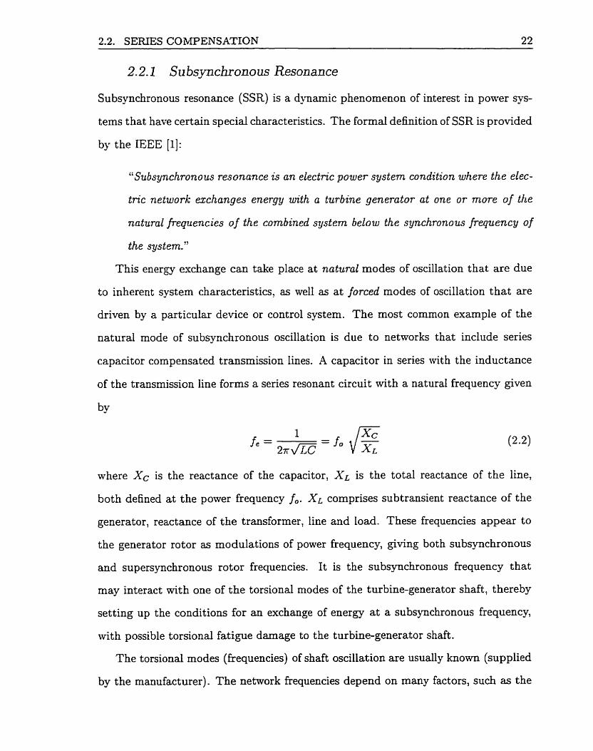
2.2.1 Subsynchronous Resonance
Subsynchronous resonance (SSR) is a dynamic phenomenon of interest in power sys-
tems that have certain special characteristics. The formal definition of SSR is provided
by the IEEE [l]:
"Subsynchronous resonance zs an electrïc power system condition where the elec-
tric network exchanges energy with a turbine generator at one or more of the
natural frequencies of the combined system below the synchronow frequency of
the system."
This energy exchange can take place at natural modes of oscillation that are due
to inherent system characteristics, as well as at forced modes of oscillation that are
driven by a particular device or control system. The most common example of the
natural mode of subsynchronous oscillation is due to netmorks that include series
capacitor compensated
of the transmission line
by
transmission lines. A capacitor in series with the inductance
forms a series resonant circuit with a natural frequency given
where Xc is the reactance of the capacitor, XL is the total reactance of the line,
both defined at the power frequency f,. X L comprises subtransient reactance of the
generator, reactance of the transformer, line and load. These frequencies appear to
the generator rotor as modulations of power frequency, giving both subsynchronous
and supersynchronous rotor frequencies. It is the subsynchronous frequency that
may interact with one of the torsional modes of the turbine-generator shaft, thereby
setting up the conditions for an exchange of energy a t a subsynchronous frequency,
with possible torsional fatigue damage to the turbine-generator shaft.
The torsional modes (frequencies) of shaft oscillation are usually known (supplied
by the manufacturer). The network frequencies depend on many factors, such as the
2.2. SERTES COMPENSATION 23
amount of series capacitance in service and the network switching arrangements at
a particular time. A series capacitor compensated transmission network can cause
sustained or negatively damped subsynchronous oscillations by two distinctive mech-
anisms, viz., self excitation due to induction generator effect and interaction \vit h
torsional oscillations.
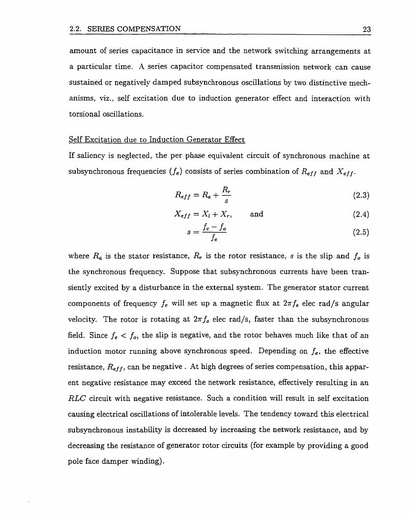
Self Excitation due to Induction Generator Effect
If saliency is neglected, the per phase equivalent circuit of synchronous machine at
subsynchronous frequencies ( fe) consists of series combination of Re ff and Xe
Rt Re,, = Ra + - S
and
where Ra is the stator resistance, R, is the rotor resistance, s is the slip and f, is
the synchronous frequency. Suppose that subsynchronous currents have been tran-
siently excited by a disturbance in the external system. The generator stator current
components of frequency f, will set up a magnetic flux a t 2 r f , elec rad/s angular
velocity. The rotor is rotating at 27&, elec rad/s, faster than the subsynchronous
field. Since fe < fol the slip is negative, and the rotor behaves much like that of an
induction motor running above synchronous speed. Depending on f,, the effective
resistance, Rej!, can be negative . At high degrees of series compensation, this appar-
ent negative resistance may exceed the network resistance, effectively resulting in an
RLC circuit with negative resistance. Such a condition nrill result in self excitation
causing electrical oscillations of intolerable levels. The tendency toward this electrical
subsynchronous instability is decreased by increasing the network resistance, and by
decreasing the resistance of generator rotor circuits (for example by providing a good
pole face damper winding) .
2.3. COUNTERMEASURES TO SSR 24
Torsional Interaction
Torsional interaction occurs when the induced subsynchronous torque in the generator
is close to one of the torsional natural modes of the turbine-generator shaft. In other
words if the cornplernent of the natural frequency (f,-f,) of the network is close to one
of the torsional frequencies of the turbine-generator shaft system, torsional oscillations
can be excited. Under such conditions, a small voltage induced by rotor oscillations
can result in large subsynchi-onous currents, this current will produce an oscillatory
cornponent of rotor torque. Moreover, the induced subsynchronous frequency voltage
is phased to sustain the subsynchronous torque. If this torque equals or esceeds the
inherent mechanical damping of the rotating system, the coupled electromechanical
system will experience growing oscillations.
The machines which are most susceptible to SSR are large multiple-stage stearn
turbines, mhich typically have four or five torsionai modes in subsynchronous fre-
quency range. The consequences of a SSR condition can be dangerous in the short
term, if the oscillations are unstable and build up sufficiently, the shaft can break.
But even if oscillations are relatively well damped, disturbances (like switching, fault
clearing, etc.) can diminish the shaft life due to mechanical fatigue.
2.3 COUNTERMEASURES TO SSR
There are two conditions that create little or no concern regarding SSR for estensive
application of series compensation.
1. The first condition is where the generators connected to the system are driven
by hydraulic turbines. In the hydro-turbine generator system, the ratio of gen-
erator mass is significantly higher than the corresponding ratio of steam-turbine
generator system. The large mass of the hydro generator increases the effective
modal damping and modal inertia making it essentially impossible to excite the
natural torsional frequencies of the turbine generator system.
2.4. POWER SYSTEM MODELING 28
2. When generators are connected to the noncompensated 230 kV lines, which in
turn are connected to highly compensated 500 kV lines. The 230 kV circuits
act to shield the turbine-generator units frorn strong interactions wit h the series
compensated lines.
A wide variety of methods have been proposed in the literature for darnping SSR
oscillations [2], such as the use of excitation control [3], Static Var Compensator
(SVC) [4, 5. 61, NGH (N.G. Hingorani) scherne [7], static phase-shifter [8]: super
conducting magnetic energy storage (SMES) [9], etc. In this investigation the effec-
tiveness of a STATCOM in darnping SSR oscillations is evaluated.
2.3.1 Static Synchronous Compensa tor (STATCOM)
The availability of high power gate turn-off switching devices (GTO, IGBT) have
recently led to the development of a new equipment called static synchronous com-
pensator (STATCOM) [IO, 111. STATCOM is a second generation FACTS equipment
based on a voltage source inverter. ST'4TCOM uses self commutating devices like
GTOs and is an advanced form of SVC. The operating and functional characteristics
of a STATCOM are however different from those obtained using WC. The major
advantages of a STATCOM over the conventional SVC are, significant size reduction
due to reduced number of passive elements, and ability to supply required reactive
power even at low bus voltages [12].
2.4 POWER SYSTEM MODELING
Torsional interaction effects involve energy interchange between the turbine-generator
shah system and the inductance/capacitances of the network. Therefore, the analysis
of SSR problems requires representation of both the electromechanical dynamics of
the generating units, and the electromagnetic dynamics of the transmission network.
The turbine-generators and their prirnary controls, the speed governors and excitation
systems are represented in detail by their differential equations. The network is also


2.4. P O W R SYSTEM MODELING 27
Mechanical damping is assumed to be zero for al1 masses to represent the worst
damping conditions. The generator is equipped with a static excitation system. The
configuration for the static excitation and the governor systern are taken from [El.
The system data and the initial operating conditions of the system are given in the
Combining the equations of mechanical system, generator, excitation system, gov-
ernor system, and the capacitor compensated transmission Iine results in a set of 2 ~ ' ~
order nonlinear differential equations without ST.4TCOM. These differential equa-
tions are then linearized around an operating point to obtain the linear differential
equations which are then used to obtain the system eigenvalues. The six-mass mode1
of Figure 2.1 has five torsional modes in addition to an electromechanical mode (mode
O). The IEEE first benchmark system is characterized by four unstable torsional
modes. Each of these modes has its Iargest SSR interaction at a certain value of
the series compensation Xc [6]. It is to be noted that the definition of % series
compensation used is
where, 0.14 is the sending end transformer reactance, 0.5 is the transmission line re-
actance, and 0.06 is the equivalent system reactance at infinite bus. Without STAT-
COM, the real part of the eigenvalues corresponding to the various torsional frequen-
cies Vary in magnitude and become unstable at different levels of series compensation
as shown in Figure 2.2. For each of the critical compensation levels a t which the real
part of the eigenvalue is maximum (indicating worst damping), the corresponding
torsional and electrical mode eigenvalues of the system without STATCOM are listed
in Table 2.1. From Figure 2.2 it can be seen that modes 1,2,3 and 4 become unstable
at various compensation levels. The objective is to damp al1 these torsional modes
by employing STATCOM at the generator terminal.

2.5. STATCOM MODEL 28
15.76 Hz Mode L
Mode 5 47.43 Hz
I I I I 1 1
10 20 30 40 50 60 70 80 90 100 % Compensation
Figure 2.2: SSR modes of first benchmark mode1
Table 2.1: First benchmark eigenvalues
Mode 1- 32%
O
1
2 3
4
5
ele
% Compensation Level
2.5 STATCOMMODEL
The state space mode1 in R-I frame (the synchronously rotating frame of reference)
for the STATCOM circuit in Figure 2.1 can be written as below. It is to be noted
that the per unit system adopted for modeling the STATCOM circuit is the same as
2.6. STATCOM CONTROLLER 29
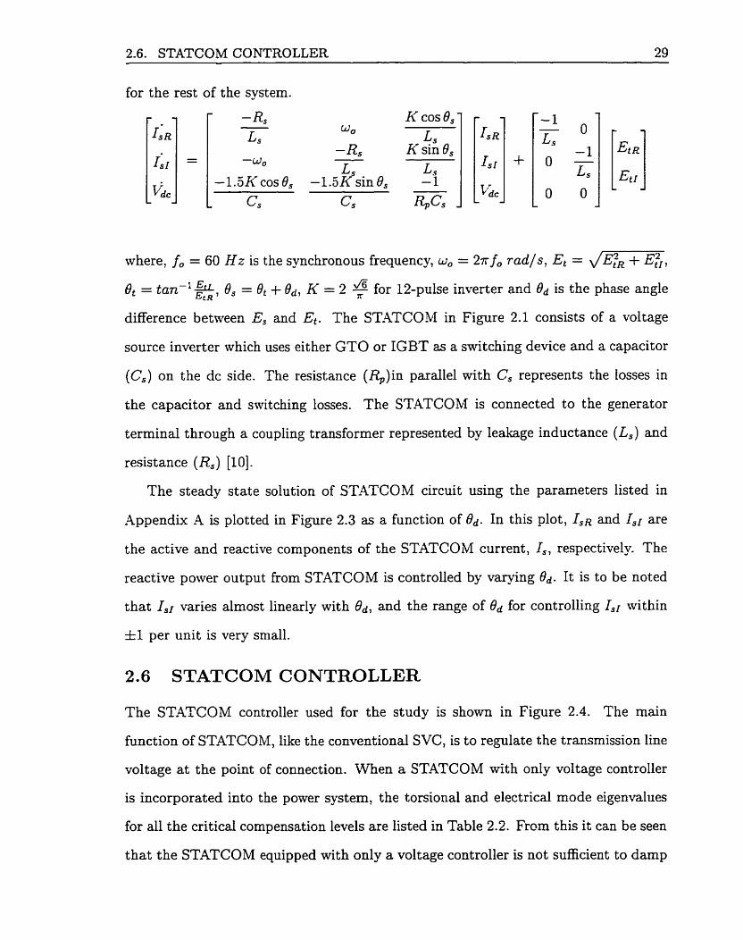
for the rest of the system.
L s -1.5K cos 8, -l.SK sin 8,
where, fo = 60 Hz is the synchronous frequency, w0 = 2nf, radis , Et = d m , Bt = tan-' &, 0, = Or + Od, K = 2 $ for 12-pulse inverter and Od iç the phase angle
difference between Es and Et. The ST.4TCOM in Figure 2.1 consists of a voltage
source inverter which uses either GTO or IGBT as a switching device and a capacitor
(Cs) on the dc side. The resistance (%)in parallel with Cs represents the losses in
the capacitor and switching losses. The STATCOM is connected to the generator
terminal through a coupling transformer represented by leakage inductance (L,) and
resistance (R,) [IO].
The steady state solution of ST.4TCOM circuit using the parameters listed in
Appendix -4 is plotted in Figure 2.3 as a function of Bd. In this plot, IsR and ISI are
the active and reactive components of the STATCOM current, I,, respectively. The
reactive power output from STATCOM is controlled by varying Bd. It is to be noted
that ISI varies almost linearly with Bd, and the range of Bd for controlling IsI within
hl per unit is very small.
2.6 STATCOM CONTROLLER
The STATCOM controller used for the study is shown in Figure 2.4. The main
function of STATCOhI, like the conventional SVC, is to regulate the transmission line
voltage a t the point of connection. When a STATCOM with only voltage controller
is incorporated into the power system, the torsional and electrical mode eigenvalues
for al1 the critical compensation Ievels are listed in Table 2.2. Fmm this it can be seen
that the STATCOM equipped with only a voltage controller is not sufficient to damp

2.6. STATCOM CONTROLLER 30
Figure 2.3: S teady state characteristics of STATCOM
Et - K D I ~ I
Figure 2.4: STATCOM controller
2.6. STATCOM CONTROLLER 31
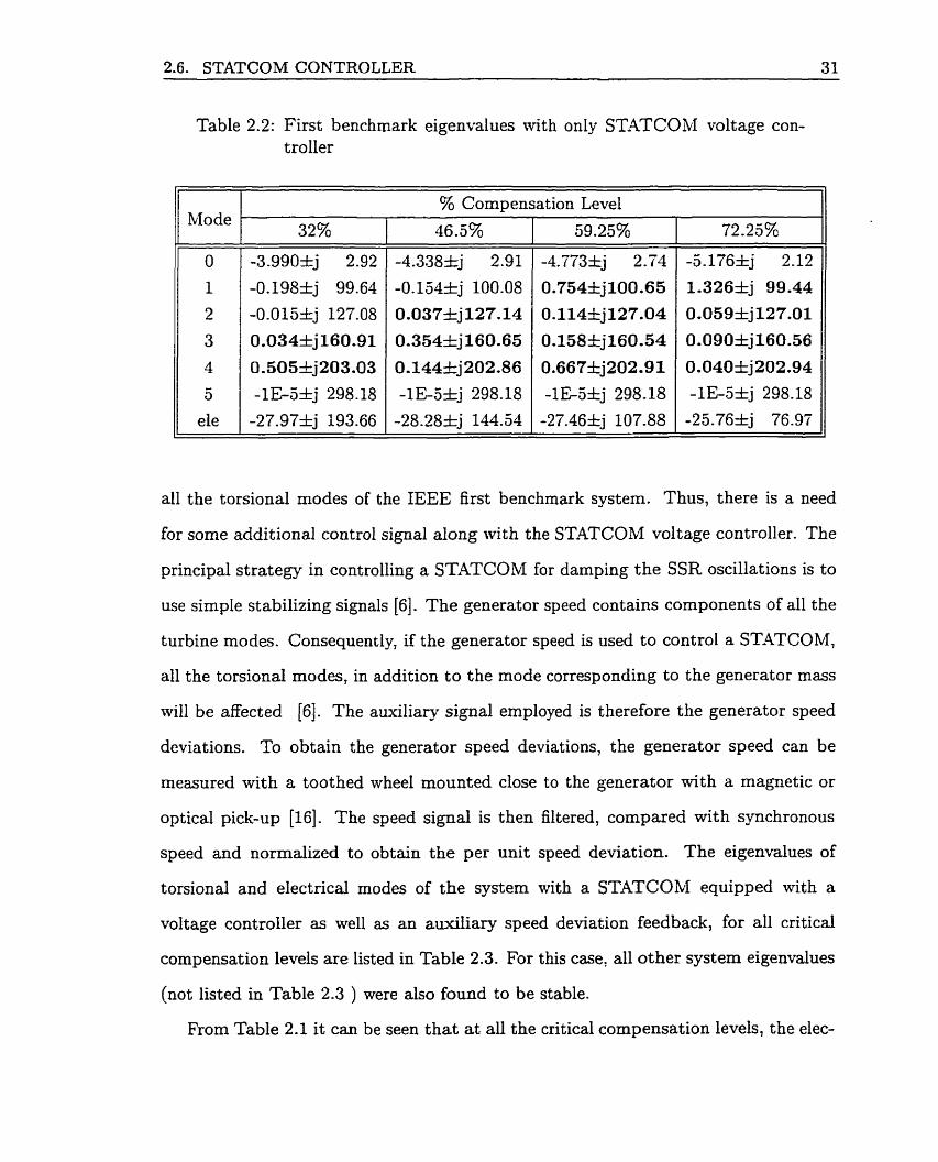
Table 2.2: First benchmark eigenvalues with only ST.2SCOM voltage con-
Mode
O
1
2
3
4
5
ele
t roller
% Compensation Level
al1 the torsional modes of the IEEE first benchmark system. Thus, there is a need
for some additional control signal along with the STATCOM voltage controller. The
principal strategy in controlling a STATCOM for damping the SSR oscillations is to
use simple stabilizing signals [6]. The generator speed contains components of al1 the
turbine modes. Consequently, if the generator speed is used to control a ST.4TCOM,
ail the torsional modes, in addition to the mode corresponding to the generator m a s
will be affected [6]. The auxiliary signal employed is therefore the generator speed
deviations. To obtain the generator speed deviations, the generator speed can be
rneasured with a toothed wheel mounted close to the generator with a magnetic or
optical pick-up [16]. The speed signal is then filtered, compared with synchronous
speed and normalized to obtain the per unit speed deviation. The eigenvalues of
torsional and electrical modes of the system with a STATCOM equipped with a
voltage controller as well as an auxiliary speed deviation feedback, for al1 critical
compensation levels are listed in Table 2.3. For this case, al1 other system eigenvalues
(not listed in Table 2.3 ) were also found to be stable.
From Table 2.1 it can be seen that at al1 the critical compensation levels, the elec-
2.7. SELECTION OF CONTROLLER GAINS 32
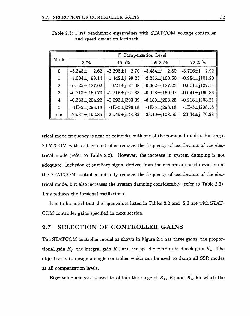
Table 2.3: First benchmark eigenvalues with STATCOM voltage controller and speed deviation feedback
-Mode
O
1
2
3 4
5
ele
% Compensation Level
trical mode frequency is near or coincides with one of the torsional modes. Putting a
ST-4TCOM with voltage controller reduces the frequency of oscillations of the elec-
trical mode (refer to Table 2.2). However, the increase in system damping is not
adequate. Inclusion of auxiliary signal derived from the generator speed deviation in
the STATCOM controller not only reduces the frequency of oscillations of the elec-
trical mode, but also increases the system damping considerably (refer to Table 2.3).
This reduces the torsional oscillations.
It is to be noted that the eigenvalues listed in Tables 2.2 and 2.3 are with STAT-
COM controller gains specified in next section.
2.7 SELECTXON OF CONTROLLER GAINS
The STATCOM controller mode1 as shown in Figure 2.4 has three gains, the propor-
tional gain Kp, the integral gain Ki, and the speed deviation feedback gain Ku. The
objective is to design a single controller which can be used to damp al1 SSR modes
a t al1 compensation levels.
Eigenvalue analysis is used to obtain the range of Kp, Ki and K, for which the

2.8. DIGITAL SIMULATION 33
system is stable. It is found that the system is stable for -6.25 5 Kp 5 -1: - 132 5
Ki 5 O and 4 5 K, < 11. From these Kp, Ki and Ku values, final gain parameters
are then selected by carrying out a step response test on the systern and ensuring that
the system settling time and the overshoot in the generator speed is low. The final
values of Kp, Ki and K, thus obtained are -1, -1.25, and 8 respectively. For these
gains, the plots of generator rotor angle and generator speed for a 10% step increase
in lcef for 72.25% compensation are shown in Figure 2.5.
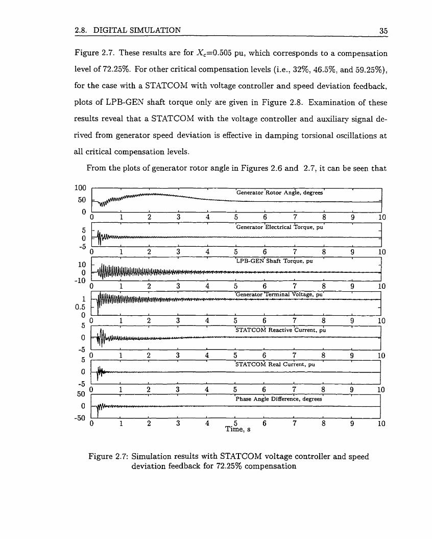
2.8 DIGITAL SIMULATION
To support the results of the eigenvalue analysis given in Tables 2.2 and 2.3, a time
domain simulation based on nonlinear differential equations of the system under a
three-phase fault at the infinite bus is performed. -4 set of nonlinear differential
Speed 1 pu = 377 radis
5 6 Time, s
Fipure 2.5: 10 % s t e ~ change in K,F for 72.25% compensation

2.8. DIGITAL SIMULATION 34
equations are solved using the fourth-order Runge-Kutta algorithm. -411 system non-
linearities are included in the model. The three-phase fault is initiated at 0.2 second:
and the fault duration is 5 cycles (83 ms). Plots of the generator rotor angle, gen-
erator electrical torque, LPB-GEN shaft torque, generator terminal voltage, and the
phase angle difference are given in Figure 2.6 for the case with a STrZSCOM under
voltage control but with no speed deviation feedback. For the case with STATCOM
under voltage control and with speed deviation feedback, in addition to the above
plots, plots of real and reactive components of ST.4TCOM current are also given in
100 1 I I 1 Generator Rotor Angle, degrees
- - 10
Generator Electrical Torque, pu r I 1
--
20 r LPB-GEN Shaft Torque, pu
I I 1
Generator Terminal Voltage, pu 1.5 . ,
-60 . I t J
O O. 1 0.2 0.3 0.4 0.5 0.6 0.7 0.8 0.9 1 Time, s
1
0.5
n w
20 - Phase Angle Daerence, degrees
Figure 2.6: Simulation results with only STATCOM voltage controller for 72.25% compensation
- -
0 . -20 -40
r
- - -
2.8. DIGITAL SIMULATION 35
Figure 2.7. These results are for Xc=0.505 pu, which corresponds to a compensation
level of 72.25%. For other critical compensation levels (Le., 32%, 46.5%: and 59.25%),
for the case with a STATCOM with voltage controller and speed deviation feedback,
plots of LPB-GEN shaft torque only are given in Figure 2.8. Esamination of these
results reveal that a STATCOM with the voltage controller and auxiliary signal de-
rived from generator speed deviation is effective in damping torsional oscillations at
al1 critical compensation levers.
From the plots of generator rotor angle in Figures 2.6 and 2.7, it c m be seen that
1 1 1
Generator Rotor Angle, degrees -
1 I I L . I I 1 l
Generator EIectncai Torque, pu 1
'Generator Terminal Voltage, pu' I
-
I I I 1
'STATCOM Reactive Current, pu r
4
1 ' I L I I O 1 2 3 4 5 6 7 8 9 10
I I I I 1
STATCOM Real Current, pu
O 1 2 3 4 5 6 7 8 9 1 O I 6 I I 1 I I I I
Phase Angle Difference, degrees 1
4 5 6 7 Time, s
Figure 2.7: Simulation results with STATCOM voltage controller and speed deviation feedback for 72.25% compensation

2.8. DIGITAL SIMULATION 36
59.25% compensation 5
2 O
O 1 2 3 4 5 6 7 8 9 10 Time, s
Figure 2.8: LPB-GEN shaft torques for ot her critical compensation Ievels with STATCOM voltage controller and speed deviation feedback
imrnediately after the occurrence of the fault, the generator rotor angle decreases for a
few tenths of a second before increasing. This is due to the presence of the STATCOM.
At the onset of the fault, the generator terminal voltage transiently drops to zero for
a few tenths of a second. The STATCOM voltage controller tries to boost the voltage
by supplying reactive power. In this process, the STATCOM draws real power (refer
to the plot of STATCOM real current in Figure 2.7) to keep the dc side capacitor
charged [17].
From the plots of ISR and Isr in Figure 2.7 it can be seen that, in steady state,
is nearly zero, and IsI has a value of 0.35 pu. Since the STATCOM bus voltage Es is

2.9. CHAPTER SUMMARY 37
considered as 0.93, the pu MVA of ST44TCOM is 0.33. This implies that the size of
ST.4TCOM required would be of the order of 30-35% of the generator MVA rating.
2.9 CHAPTER SUMMARY
In this chapter, a new concept of using a STATCOM to damp the torsional subsm-
chronous oscillations in addition to controlling the voltage in power system has been
proposed. The concept is verified bj- rneans of eigenvalue analysis and detail tirne do-
main simulations under a severe three-phase fault at the infinite bus. Application of
this concept to the IEEE first benchmark system proved that a STATCOM, provided
at the generator terminal and equipped with both voltage controller and an auxiliary
signal derived from generator speed deviation is effective in damping the torsional
oscillations at al1 compensation levels.
Bibliography
IEEE SSR Working Group: "Proposed terms and definitions for subsynchronous
resonance," IEEE Publication, vol. 81 TH0086-9-PWR, pp. 92-97, 1981.
IEEE Cornmittee Report, "Countermeasures to subsynchronous resonance prob-
lems," IEEE Transactions on Power Apparatus and &stems, vol. 99. no- e, PP-
1810-1817, 1980.
-4. Yan and Y.N. Yu, "klulti-mode stabilization of torsional oscillations using
output feedbacli excitation control," IEEE Transactions on Power Apparatus
and Systems, vol. 101, no. 5, pp. 1245-1253, 1982.
T.H. Putman and D.G. Ramey, "Theory of the modulated reactance solution
for subsynchronous resonance," IEEE Transactions on Power Apparatw and
Systems, vol. 101, no. 6 , pp. 1327-1533, 1982.
O. Wasynczuk, "Damping subsynchronous resonance using reactive power con-
troi," IEEE Transactions on Power Apparatus and Systems, vol. 100, no. 3, pp.
1096-1103, 1981.
A.E. Harnmad and M. El-Sadek, "Application of a thyristor controlled var com- pensator for damping of subsynchronous oscillation^ in power system," IEEE Transactions on Power Apparatw and Systems, vol. 103, no. 1, pp. 198-212,
1984.
N.G. Hingorani, "A new scheme for subsynchronous resonance damping of tor-
sional oscillations and transient torques-part 1,7' IEEE Transactions on Power
Apparatus and Systems, vol. 100, no. 4, pp. 1852-1855, 1981.
M.R. Iravani and R.M. Mathur, "Damping of subsynchronous oscillations in
power systern using a static phase-shifter," IEEE Transactions on Power Deliv- ery, vol. 1, no. 2, pp. 76-83, 1986.
GJ. Wu and Y-S. Lee, "Application of simultaneous active and reactive power
modulation of super conductiong magnetic energy storage unit to damp turbine
generator subsynchronous oscillations," IEEE Transactions on Energy Conver-
sion, vol. 8, no. 1, pp. 63-70, 1993.
C.D. Schauder and H. Mehta, "Vector analysis and control of advanced static
var compensators," IEEE Proceedings-C, vol. 140, no. 4, pp. 299-306, 1993.

[Il] L. Gyugyi, "Dynamic compensation of ac transmission lines by solid-state syn-
chronous voltage sources," IEEE Transactions on Power Delivery, vol. 9: no. 2,
pp. 904-911, 1994.
[12] C.W. Edwards, P.R. Nannery, K.E. Mattern, E.J. Stacey, and J. Gubernick,
''-4dvanced static var generator employing GTO thyristors," IEEE Transactions
on Power Delivery, vol. 3, no. 4, pp. 1622-1627, 1988.
[13] IEEE SSR Task Force, "First benchmark mode1 for cornputer simulation of sub-
synchronous resonance," IEEE Transactions on Power Apparatus and Systems,
vol. 96, no. 5, pp. 1565-1870, 1977.
[14] P. Kundur, Power System Stabilzty and Control, McGraw-Hill, Inc., New York,
1994.
[le] Y.N. Yu, Electric Power System Dynamics, Academic Press, New York, 1983.
[16] S. Svensson and K. Mortensen, "Damping of subsynchronous oscilIations an
hvdc link - an hvdc simulator study," IEEE Transactions on Power Apparatus
and Systems, vol. 100, no. 3, pp. 1431-1437, 1981.
[l?] J.B. Ekanayake and N. Jenkins, "-4 three-level advanced static var compensator,"
IEEE Transactions on Power Delivery, vol. 11, no. 1, pp. 540-545, January 1996.
Chapter 3
NIULTILEVEL BINARY VOLTAGE SOURCE INVERTER
3.1 INTRODUCTION
As the voltage and current ratings and switching characteristics of power electronics
devices and systems keep improving, the range of their applications and electronic
circuit concepts continues to expand. Power electronics applications in high voltage
direct current (hvdc) transmission, active filters, static var compensators (SVC), etc.
have been found to be very efficient and tightly controllable. In this chapter' struc-
ture and principle of operation of a new multilevel binary voltage source inverter is
introduced.
With the imminent deregdation of electricity markets in the near future, electric-
ity providers are looking for reliable, safe, efficient, and precise means of controlling
the power system network. The advanced high power electronics promise revolution-
ary increase in the performance. Rexibility, and cost-effectiveness of the electricity
transmission, distribution, and end-use. These improvements will help electricity
providers adapt to and exploit tomorrow7s cornpetitive power markets. Moreover, the
'A version of this chapter has been published. K.V. Patil, R.M. Mathur, J. Jiang, and S.H. Hosseini, "Distributed System Compensation using a new Binary Multilevel Voltage Source Lnverter", Paper# PE004-PWRD-0-07-1998, presented in IEEE PES summer meeting July 1998 and accepted for publication in IEEE Transactions on Power D elivery.
3.1. INTRODUCTION 41
operational flexibility they introduce d l enable eiectricity providers to significantl y
increase asset utilization and deliver new value-added customer services.
Power electronic technologies are analogous to low power transistors and inte-
grated circuits but operating a t multi-megawatt power levels. As such, they offer
long-lived solid-state devices in place of the clums';, wear-prone mechanical switches
and systems currently employed for control of transmission and distribution networks.
These electronics enable full realization of FA4CTS and Custom Power technologies,
with potential for optimum tuning and precise control of al1 power circuits.
After the advent of fast acting, forced commutating GTOs, IGBTs and the concept
of flexible ac transmission systems (FACTS) [l], a number of power electronics devices
have been proposed for dynamic compensation, improving system stability, directing
power flows, etc. [2]. A voltage source inverter (VSI), which converts dc voltage
into a single or polyphase ac voltage at a desired amplitude and frequency, is the
most prominent power electronics device discussed in the literature in the context of
reactive power compensation. The inverters with a rating ranging from 100 W to 20
MW and more are now available in industrial and commercial products [3].
Nonet heless, while t hese power electronics systems offer greater efficiency and
tighter control, they also present their users with a real problem: the contamina-
tion of the power system network by currents whose frequencies are harrnonics of the
system's synchronous frequency. However, a t the same time, these advanced power
electronics systems also help in reducing the harmonics flowing in the power system.
The inverter switches are connected and disconnected at discrete time instant to gen-
erate desired output voltage of specific magnitude and frequency. Such an output
voltage in addition to its fundamental component, contains a lot of other undesired
harrnonic components as well. To minimize harrnonic injection from an inverter into
the system, various multilevel voltage source inverter configurations have been sug-
gested. [4, 51. The multilevel inverters usually synthesize a staircase voltage wave
3.2. PRINCXPLE OF OPERATION 42
from several levels of dc voltage sources, typically obtained from capacitor voltage
sources. As the number of levels increases, the synthesized staircase wave approaches
the sinusoidal wave resulting in reduced harmonic distortion [6]. The goal here is to
minimize the harmonic distortion in the system, but a t the same time the inverter
scheme should be simple and compact. The different multilevel VSI schemes stud-
ied and tested so far include diode-clamp, Aying-capacitor and cascaded separate dc
source inverters [4]. -4 number of separate dc source inverter topologies are suggested
in [7, 8, 91.
This chapter presents
O a new multilevel binary voltage source inverter (BVSI) structure and its prin-
ciple of operation,
r a controller scheme to regulate the capacitor voltages,
the equations for the calculation of dc side capacitor values,
a selective harmonic elimination modulation (SHEM) algorit hm to eit her elim-
inate or minimize 5'h, llth, 13th, 1Yh7 and lgth order harmonics, and
rn IGBT7s firing circuit algorithm optimized from the point of microcontroller
implement ation.
3.2 PRINCIPLE OF OPERATION
Multilevel inverters can reach high voltages and reduce harmonic distortion because
of their structure. To increase the voltage rating a number of single-phase full bridge
inverters (FBI) can be connected in series. This structure automatically leads to
reduced harmonic distortion, which is desirable. However, the need to balance ca-
pacitor voltages, complexity of switching and size of capacitors, limit the number of
levels that can be practically employed.
Figure 3.1 shows the three-phase star-connected arrangement of the proposed

3.2. PRINCTPLE OF OPERATION 43
1 ELECTRICAL POWER SYSTEM NETWORK 1
I 1 I 1 1 1 1
Figure 3.1: Three-phase star connected blevel BVSI
- - pp - .
A -4 ----- ......................... + B A C
t csa
separate dc source 3-level bina- voltage source inverter.
phase FBIs connected in series. Each FBI has its own dc
of each dc source is in binary proportion of Vdc, 2Vk, and
I
It consists of three singie-
source. But the magnitude
4Vdc, where Vd, is chosen to
Coupling transformer or Interface reactor
get the desired fundamental ac voltage output for normalized one per unit modulation
index. The switches are turned-on and -off to generâte a 15-step ac voltage output
over one fundamental cycle. In generai, n-level BVSI would produce (2"+' - 1)-steps
ac voltage output as against (272 + 1)-steps output generated by a conventional n-level
separate dc source VSI configuration. This new inverter scheme does not require any
transformers, clamping diodes or flying capacitors.

3.2. PFUNCIPLE OF OPERATION 44
Figure 3.2 illustrates the ac voltage output of each level which is also a conduction
period of each capacitor (v i l , vl2, v13), the resulting ac phase voltage (va,), and the
fundamental output voltage (va) of the 3-level inverter shown in Figure 3.1. The
output phase voltage is given by:
where,
el e2 9, e4 8586875 3T 3lr - 2
Figure 3.2: T v ~ i c d voltages of 3-level BVSI
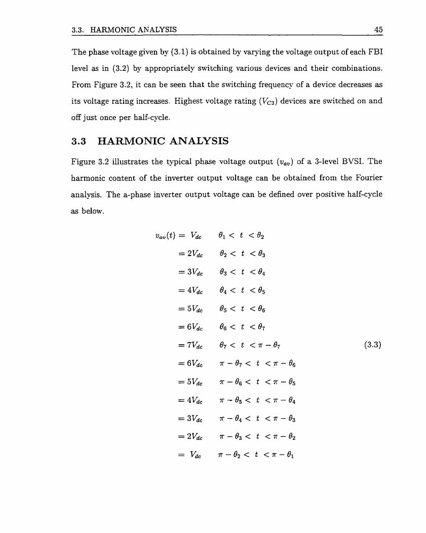
3.3. HARMONIC ANALYSIS 45
The phase voltage given by (3.1) is obtained by vaqing the voltage output of each FBI
level as in (3.2) by appropriately slvitching various devices and their combinations.
From Figure 3.2, it can be seen that the switching frequency of a device decreases as
its voltage rating increases. Highest voltage rating (TTC3) devices are switched on and
off just once per half-cycle.
3.3 HARMONIC ANALYSIS
Figure 3.2 illustrates the typical phase voltage output (va,) of a 3-level BVSI. The
harmonic content of the inverter output voltage can be obtained from the Fourier
analysis. The a-phase inverter output voltage can be defined over positive half-cycle
as below.

3.3. HARMONIC ANALYSIS 46
The Fourier frequency components of this wave can be given as
a,, = a, + ah cos (hwt) + bh sin(hwt)
However, this waveform is a symmetric, odd function (f (t) = - f (-t))' and since
f (t) = - f (t + x), it contains only odd harmonies.
Therefore,
va, = bh sin(hsrt) for h = 1,3,5,7, . . . (3.5)
The waveform also possess quarter-wave symmetry, so bh can be determined as below.
= - - cos(hwt)] :: + [- 2 cos ( b t ) ] & + [-3 c o s ( h t ) ] 7rh 4vd, [[

3.4. REDUCTION OF HARMONICS 47
-- - 41'k 2 cos(hOi) for h = 1 , 3 , 5 , 7 ; . . lïh .
Assuming bh = Û2k-1: for k = 1, 2> 3, 4,. . . , (3.5) and (3.11) can be written as
Thus for n-level binary voltage source inverter (3.13) can be modified as
From (3.12) and (3.14), a-phase inverter output voltage is given by
From (3.15), fundamental rms, harmonic rms, and maximum fundamental phase volt-
ages can be detemined as
2"-1
va =- 4Vdc C cos B, fi /2" i=l
2n-1
Kk-L = 4 v d c C COS[(^^ - 1)Bi] for k = 1,2,3, . . . \/Z (2k - l ) ~ i= 1
3.4 REDUCTION OF HARMONICS
3.4.1 IEEE Standard 51 9-1 992 on Haxmonics
IEEE Standard 519-1992, IEEE Recommended Practices and Requirements for Har-
rnonic Control in Electrical Power Systems, addresses harrnonic limits at the consumer
3.4- REDUCTION OF HARMONICS 48
and service provider interface. This standard provides procedures for controlhg har-
monics on the power system along with recommended limits for customer harrnonic
injection and overall power system harrnonic levels to ensure overall system voltage
integrity. The utilities are responsible for maintaining the quality of voltage on the
overall system and for the voltage distortion at the point of common coupling (PCC)
as aell. Table 3.1 surnmarizes the voltage distortion guidelines for different system
voltage leveIs.
The total harmonic distortion (THD) is defined as
where,
= magnitude of individual harrnonic components (rms volts)
h = harrnonic order
Vn = nominal system voltage (rms volts)
Note that this definition is stightly different than the conventional definition for total
harrnonic distortion, which expresses the distortion as a function of the fundamental
frequency voltage magnitude at the time of the measurement. The definition used
here allows the evaluation of the voltage distortion with respect to fixed limits rather
than limits that fluctuate with the system voltage.
Table 3.1 : Harmonic voltage distortion limits
I I BUS voltage 1 Individual Harmonic 1 Total Voltage
II at PCC (vn) 1 Voltage Distortion (%) 1 Distortion- THDv, (%)
3.4. REDUCTION OF HARMONICS 49
Excessive harmonic kvels (voltage and/or current) on the utility system can result
in increased equipment heating, equipment malfunction and prernature equipment
failure, communication interference: fuse blowing in capacitor banks, and customer
equipment and process problems. When the distortion levels on the utility system
are a problem, mitigation measures need to be irnplernented.
3.4.2 SeIective Harmonic mimination Modülation Technique
In order to reduce the harmonics injected into power system by BVSI, selected har-
monics elimination modulation (SHEM) technique for this inverter configuration is
developed.
Equation (3.15) shows that the output voltage of BVSI contains odd harmonic
voltages in addition to fundamental voltage. Equations (3.16) and (3.17) show that
the fundamental voltage and harmonic voltages can be changed by varying either the
dc voltage, Vdc, or the modulation angles, ( B i ) . Varying the dc voltages is not econom-
ical in practical applications, because it then needs a rectifier. Here the modulation
angles are varied to control the fundamental output voltage as well as to minimize
the harmonic distortion.
The phase voltage va, of the 3-level BVSI is plotted in Figure 3.2, where 7-steps
are introduced in the otherwise square wave inverter output, to control the magnitude
of the fundamental voltage and to eliminate or minimize any six harmonics. On a
half-cycle basis, each step provides one degree of freedom, Le., having (2" - 1)-steps
per half-cycle in an n-level BVSI provides control of the fundamental and elimination
or minimization of (2" - 2) harmonics. Using (3.16) and (3.18), the Modulation Index,
MI, or amplitude modulation ratio is defined as

The harrnonics of the orders 5th, jrth, 1lth, 1 3 ~ ~ ~ and l g t h are either completely
eliminated or rninirnized. From (3.17)
TG = CCOS(~O~) = O for h = 5 . 7 : 11,130 17: 19
1 ewt on- The seven non-linear equations given by (3.20) and (3.21) are solved by Y
Raphson numerical technique to derive switching instant (angles) of BVSI swit ches.
It is to be noted that due to non-linear and transcendental nature of these equations,
the initial values must be close to the final solution of these equations. The solutions
for the above set of equations for the modulation index varying from 0.51 to 0.886
in steps of 0.001 are obtained. Table 3.2 lists a few of these solutions. Figure 3.3
illustrates the feasible modulation angles for these modulation indexes. Al1 t hese
solutions are obtained off-line and stored in a switching patterns table to be used
during run time.
Table 3.2: Switching patterns for blevel BVSI
Modulation Angles in degrees
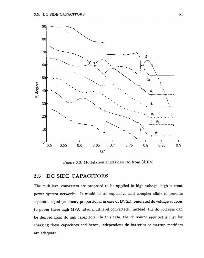
3.5. DC SIDE CAPACITORS
Figure 3.3: Modulation angles derived from SHEM
3.5 DC SIDE CAPACITORS
The multilevel converters are proposed to be applied in high voltage, high current
power system networks. It would be an expensive and complex affair to provide
separate, equal (or binary proportional in case of BVSI), regulated dc voltage sources
to power these high MVA rated multilevel converters. Instead, the dc voltages can
be derived from dc link capacitors. In this case, the dc source required is just for
charging these capacitors and hence, independent dc batteries or startup rectifiers
are adequate.

3.5. DC SIDE CAPACITORS 52
Once the dc link capacitors are charged, ideally they should maintain their charge
because other than minimal capacitor tan 6 losses, there are no other discharge paths.
However, in practice, these capacitors conduct through IGBT, GTO switches which
are non-ideal and these switches turn-on and -off a t considerable high frequencies.
The cumulative effects of switching losses, unequal capacitor leakage currents! unequal
delays in switching, and asymmetrical charging and discharging of capacitors during
disturbances contribute towards the divergence of the capacitor voltages, resulting in
the collapse of some and overcharging of others. Maintaining some reasonabie voltages
on the capacitors is important for proper operation of an inverter, but regulating
these voltages (Le., in binary proportion for BVSI) is of paramount importance for
a desirable performance from an inverter. Regulation of dc voltages is necessary
to prevent the degradation of the quality of power supply at the point of common
coupling due to harrnonics. The harmonic elimination strategies (Section 3.4.2) are
based on the assumption that the dc voltages are regulated in binary proportion.
The way to maintain adequate charges on the dc link capacitors and regulate their
voltages are devised.
3.5.1 Capacitance of DC Capacitors
The dc bus capacitors are sized (their capacitance is chosen) such that the voltage
ripple on the dc bus is uithin acceptable limits. For the proposed inverter, each FBI
as well as each phase have separate capacitors. From the first principle (definition of
capacitance), the value of individual capacitance Ci can be calculated as:
where Aqi is the deviation in the charge on the capacitor which depends upon the ca-
pacitor current waveform, Vci is the average capacitor voltage, and e is the regdation

3.5. DC SIDE CAPACITORS 5 3
factor of the capacitor voltage. The value of e rnay range from 5 - 20% for practical
use. Vci and e are defined as:
From Figure 3.2, the deviation in the charge on any capacitor can be formulated as:
where I is the rated rms phase current of the inverter, T is one cycle time period.
From (3.22) and (3.25)
Using (3.26) and Figure 3.2, the capacitance values of the BVSI shown in Figure3.1
are calculated as
To generate the
- sin + sin B2 - sin O3 + sin O4 - sin B5 + sin B6 - sin 07] (3.27)
- sin O2 + sin Bq - sin B6] (3.28)
- sin 01] (3.29)
required reactive power from the inverter, the modulation index
MI is varied and the modulation angles Bi are calculated for each MI value. When MI
is MImin the inverter absorbs the rated reactive power (BVSI bus voltage > system
bus voltage to which inverter is connected), whereas when MI is MI,, the inverter
generates the rated reactive power (BVSI bus voltage < system bus voltage to which
inverter is connected). From the switching patterns shown in Table 3.2, it c m be seen
that the modulation angles are minimum for MI=MI,,. Therefore the modulation
angles corresponding t o MI,, are used to calculate the capacitance values.
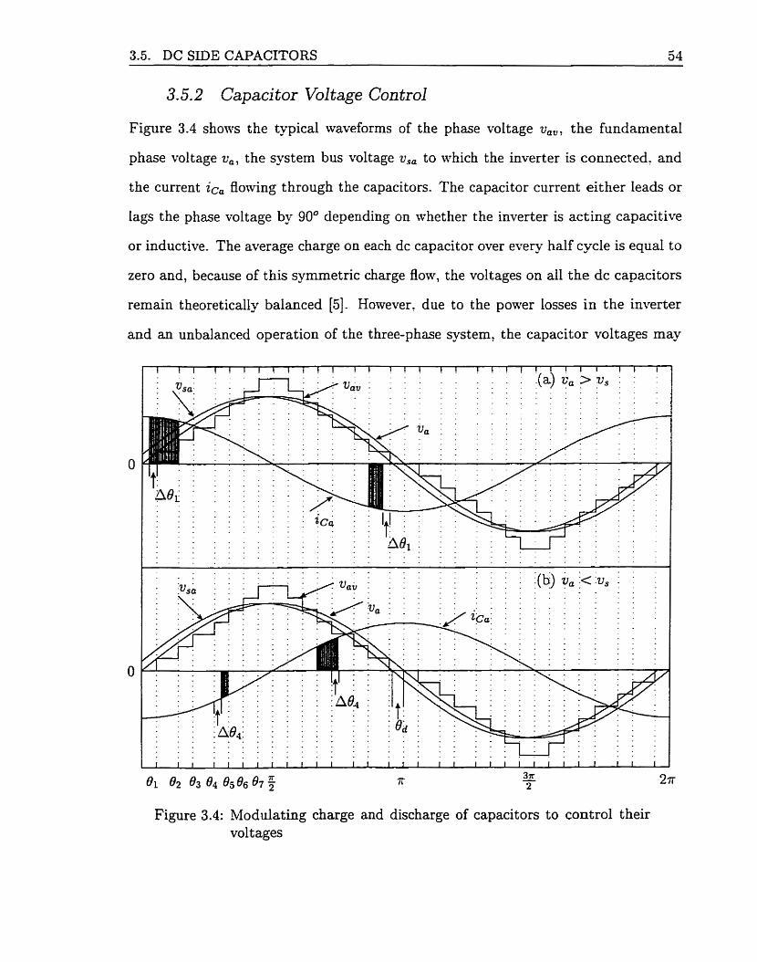
3.5. DC SIDE CAPACITORS 54
3.5.2 Capacitor Voltage Control
Figure 3.4 shows the typical waveforms of the phase voltage va,, the fundamental
phase voltage va, the system bus voltage usa to which the inverter is connected, and
the current ic, flowing through the capacitors. The capacitor current either leads or
Iags the phase voltage by 90' depending on whether the inverter is acting capacitive
or inductive. The average charge on each dc capacitor over every half cycle is equal to
zero and, because of this symmetric charge flow, the voltages on al1 the dc capacitors
remain theoretically balanced [5]. However, due to the power losses in the inverter
and an unbalanced operation of the three-phase system, the capacitor voltages may
Figure 3.4: Modulating charge and discharge of capacitors to control their voltages
3.5. DC SIDE CAPACITORS 53
drift away from their set levels.
In case of the BVSI in Figure 3.1: the set voltage levels are I&, 2C&, and 4&,.
In pnnciple, the charge and hence the voltage across each capacitor is rnaintained
by prolonging or shortening the current flow through it. This is achieved by shifting
the switching patterns [J, 8. 91. The direction of phase shift depends upon whether
the inverter is producing leading vars or absorbing lagging vars. Figure 3.4(a) depicts
extra charging of capacitor CI to raise its falling voltage when the inverter is producing
leading vars. In the positive half-cycle of ica, capacitor CL conduction is increased
by A&, whereas in the negative half cycle it is reduced by the same amount. This is
shown by the shaded areas. The shaded area in the positive half cycle is larger than
that in the negative half cycle, indicating extra charging of Cl.
Figure 3 4 b ) illustrates extra charging of capacitor C3 when the inverter is ab-
sorbing lagging vars. Here also positive half cycle conduction of C3 is more than its
negative half-cycle conduction. Similarly, O2 is modulated to adjust the conduction of
capacitor C2. The required power to charge the capacitors is drawn from the system
by controlling the phase lag Bd between va and usa as shown in Figure 3.4.
The capacitor voltage control scheme employed is shown in Figure 3.5. One such
controller on each phase maintains individual capacitor voltages in binary proportion
as well as it adjusts the phase lag between the inverter phase voltage and the system
phase voltage to draw sufficient amount of active power from the spstem required
to keep capacitors charged. The net active power drawn equals to the switching
losses and capacitor losses. In Figure 3.5 the phase lag angle Bd adjusts net active
power flow into the inverter and angles AB1, AB2, and 464 are used to prolong or
shorten the conduction of capacitors Ci, C2, and C3 respectively by shifting switching
patterns el, O*, and e4 in order as shown in Figure 3.4. It is found that normally
AB1, A&, Ag4 and ûd are each less than 1" which means that such an unegual
conduction of these capacitors is not likely to affect the three-phase system balance.

3.6. GATE PULSE GENERATION ALGORITHM 56
Figure 3.5: Capacitor voltage controller
3.6 GATE PULSE GENERATION ALGORITHM
The gate pulses are synchronized with the system voltage at the point of common
coupling. To do this usa (t) and v,. (t - At) are cornpared every time step to detect the
positive zero crossing of v,, wave. From this reference zero crossing point, a reference
signal wt is derived. When zero crossing is detected, ut is set to zero and otherwise
wt = ut + Atdeg, where Atde, = At x 360 x f, (equivalent degrees corresponding to
each sampling time step, At, at the synchronous frequency, f,) . Figure 3.6 illustrates
us, wave, derived wt signal, and corresponding gate pulses g1. . .g7. Table 3.3 shows
the digital pulse patterns for one cycle period employed in generation of four gate
pulses, gl, g3, fi, and gll , which are derived using Figure 3.6. The remaining eight
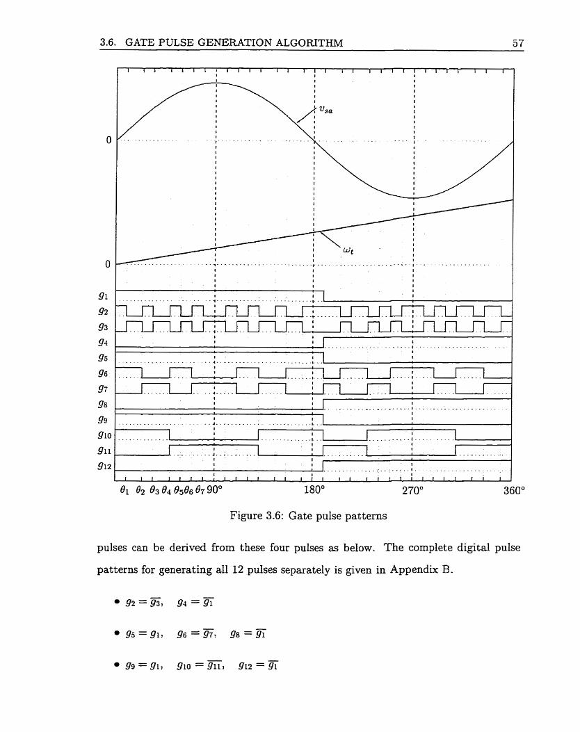
3.6. GATE PULSE GENERATION ALGORITHM
el 042 e3 O4 67 90' 180" 2 70"
Figure 3.6: Gate pulse patterns
pulses can be derived from these four pulses as below. The complete digital pulse
patterns for generating al1 12 pulses separately is given in Appendix B.
3.7. CHAPTER SUMMARY 58
In practice, in order to prevent arm shoot in the arm of an inverter, a dead
time between high and low side 0i\; gate pulses is introduced. The dead time is the
minimum separation time required between the gate pulses becoming on for both
high and low side switches in the sarne arrn of the inverter.
3.7 CHAPTER SUMMARY
A new multilevel binary voltage source inverter configuration is analyzed in this chap
ter. An n-level binary voltage source inverter produces (Zn+' - 1)-steps ac voltage
output as against (2n + 1)-steps output generated by a conventional n-level sepa-
rate dc source voltage source inverter configuration. The increase in the stair-case
output voltage waveform steps autornatically reduces the harrnonic content. To mini-
mize harmonies further, a selected harrnonic elimination technique is developed. The
equations for determining the capacitance of dc side capacitors are derived and a
controller to regulate the capacitor voltages in binary proportion is developed. A
compact gate pulse generation algorithm which is easy to implement in microcon-
troller is developed. This new inverter scheme is modular in structure and does not
require any transforrners: clamping diodes or flying capacitors.
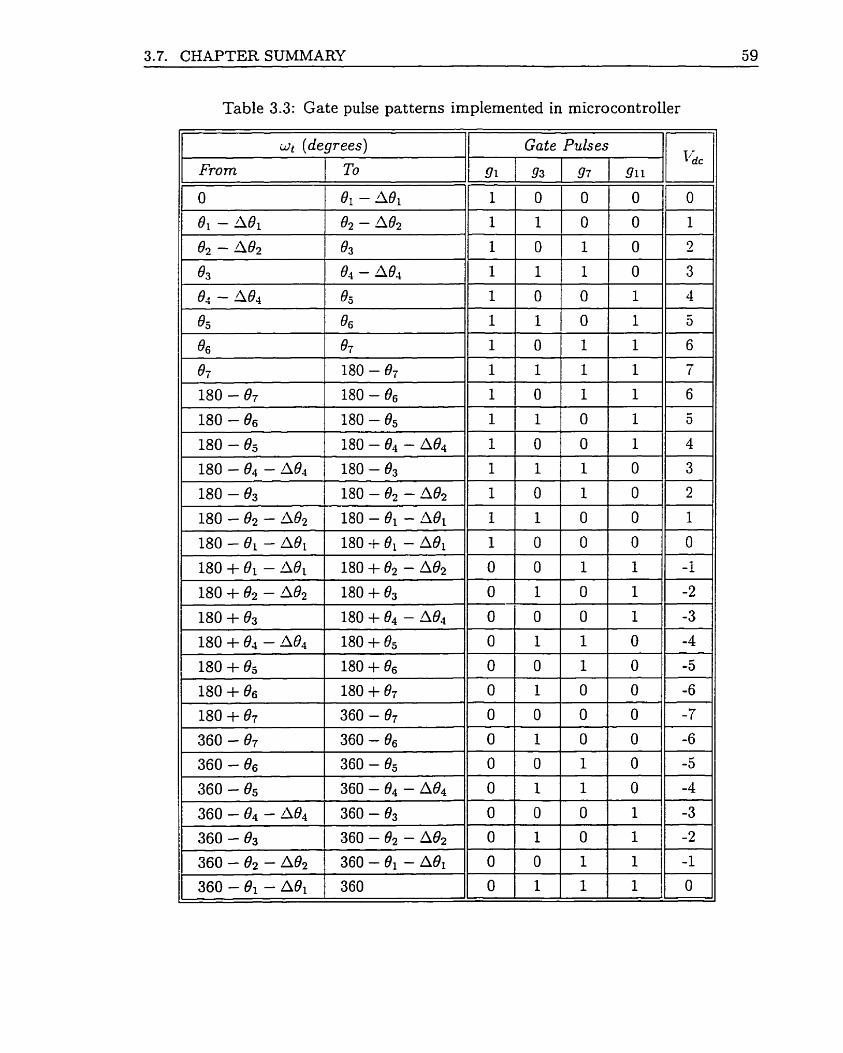
3.7. CHAPTER SUMMARY 59
Table 3.3: Gate pulse patterns imprernented in microcontroller
ut (degrees) Gate Pulses
From 1 To
Bibliography
[l] N.G. Hingorani, "High power electronics and flexible ac transmission system,"
IEEE Power Engineering Review, pp. 3-14, July 1988.
[2] L. Gyugyi, C D . Schauder, and et-al., "The unified power flow controller: a new
approach to power transmission control:" IEEE Transactions on Power Delivery,
vol. 10, no. 2, April 1995.
[3] Deepak Divan, "Low-stress stvitching for efficiency," IEEE Spectrum, pp. 33-39,
December 1996.
[4] Jih-Sheng Lai and Fang Zheng Peng, "Multilevel converter-a new breed of power
converters," IEEE Transactions on Industry Applications, vol. 32, no. 3, pp.
509-517, hiIay/June 1996.
[5] Fang Zheng Peng, Jih-Sheng Lai, John W. McKeever, and James Vancoevering,
"A multilevel voltage-source inverter with separate dc sources for static var gener-
ation," IEEE Transactions on Industry Applications, vol. 32, no. 5 , pp. 1130-1138,
September/October 1996.
[6] P.M. Bhagwat and V.R. Stefanovic, "Generalized structure of a multilevel PWM inverter," IEEE Transactions on Industrg Applications, vol. 19, no. 6, pp. 1057-
1069, November/December 1983.
[7] J.B. Ekanayake and N. Jenkins, "A three-level advanced static var compensator,"
IEEE Transactions on Power Delivery, vol. 11, no. 1, pp. 340-545, January 1996.
[8] Clark Hochgraf and R.H. Lasseter, "A transformer-less static synchronous com-
pensator ernploying a multilevel inverter," IEEE Transactions on Power Delivery,
vol. 12, no. 2, pp. 881-887, April 1997.
[9] C. J . Hatziadoniu and F.E. Chalkiadakis, "A 12-pulse static synchronous com-
pensator for the distribution systern employing the 3-level GTO-inverter," IEEE Transactions on Power Delivery, vol. 12, no. 4, pp. 1830-1835, October 1997.

Chapter 4
DYNAMIC COMPENSATION USING STATCOM
4.1 INTRODUCTION
This chapterl presents the application of BVSI as a dynamic compensator.
In an ac power system the power transmitted over a transmission line is related to
the transmission line voltage profile under steady state and dynamic conditions over a
wide range of network contingencies. Modern highly interconnected power systems are
not very tolerant of abnormal voltages, even for a short periods. Undervoltage, which
is the result of heavy loading and shortage of generation, causes degradation in the
performance of loads like induction mot ors, arc furnaces. Overvoltage, which is the
result of light loading state, is of concem as it constitutes a risk of Aashover, insulation
deterioration and/or breakdown. It is a well established practice to use reactive power
compensation to regulate the ac system voltage. The main function of a STATCOM
is to regulate the ac system voltage. It achieves this by providing controlled reactive
power support at the point of common coupling. The reactive power compensation
can increase the utilization of existing transmission system by providing controlled
'A version of this chapter has been published. K.V. Patil, R.M. Mathur, J. Jiang, and S.H. Hosseini, "Distnbuted System Compensation using a new Binary Muitilevel Voltage Source Inverter", Paper# PE004PWFD-0-07-1998, presented in IEEE PES summer meeting July 1998 and accepted for publication in IEEE Transactions on Power Delivery.

4.1. INTRODUCTION 62
reactive power to stabilize the system, improve the system darnping and regulate the
voltage profile [l, 2; 3, 41.
There are variety of devices like L.xed/switched reactors: iïxed/switched capacitors,
synchronous condensers, static var compensators that have been employed to provide
the required reactive power compensation. With the advancement in high power
electronics technology and the availability of force commutated GTO, IGBT smit ches,
application of voltage source inverters (VSI) as compensators in an electrical power
system have been suggested in the literature [l, 51. Such an inverter when connected
in shunt with a power system is referred to as a static synchronous compensator
(STATCOM or SSC). To minimize harmonic injection from a STATCOM into the
system, various multilevel voltage source inverter configurations have been suggested
in [6, 71. In this chapter the 3-level binary voltage source inverter (BVSI) studied in
Chapter 3 is examined as a shunt reactive power compensator.
This chapter presents:
a the application of a BVSI as a dynamic compensator in a 13.8 kV electrical
distribution system,
effectiveness of selective harmonic elimination algorithm in improving the qual-
ity of power supply at the point of common coupling by either minimizing or
eliminating sth, 7'h, Wh, 13'~ , IF", and l g t h harmonics,
hierarchical closed-loop controllers to regulate the load bus voltage and the
capacitor voltages, and
a t ransient simulation results for various operat ing conditions in bot h leading and
lagging mode operation of the STATCOM.

4.2. DYNAMIC COMPENSATION USING BVSI 63
4.2 DYNAMIC COMPENSATION USING BVSI
With BVSI, the dynamic compensation of the ac system at the point of common
coupling is achieved by meeting the reactive power demands in transient as well as in
steady state conditions. To generate the required reactive power from the inverter,
the modulation indes MI is varied and the gate firing angles Bi are calculated for each
MI value. When MI is MI,, the inverter absorbs the rated reactive ponTer (inductive
STA4TCOM), whereas when MI is MI,, the inverter generates the rated reactive
power (capacitive ST.4TCOM).
Figure 4.1 shows the configuration of a distribution system studied for esamining
the effectiveness of the BVSI to regulate the load bus voltage under various operating
condit ions.
The distribution system considered is 13.8 kV, 60 Hz with short circuit capacity
of 100 MV.4 and X / R = 4. A three-phase, 3-level, 15-step, f 15 b1VIV.R BVSI is
connected to the load bus through 10 mH interface reactor. The load considered is
10 MW + 8 MVAR.
z t 15 MVAR BVSI
I vc2
13.8 kV 60 Hz
swrrm 3 CAPACITOR 7 RRING + , VOLTAGE . LOGIC C-- CONTROL
Voltage Controller
Figure 4.1: Distribution system compensation using BVSI
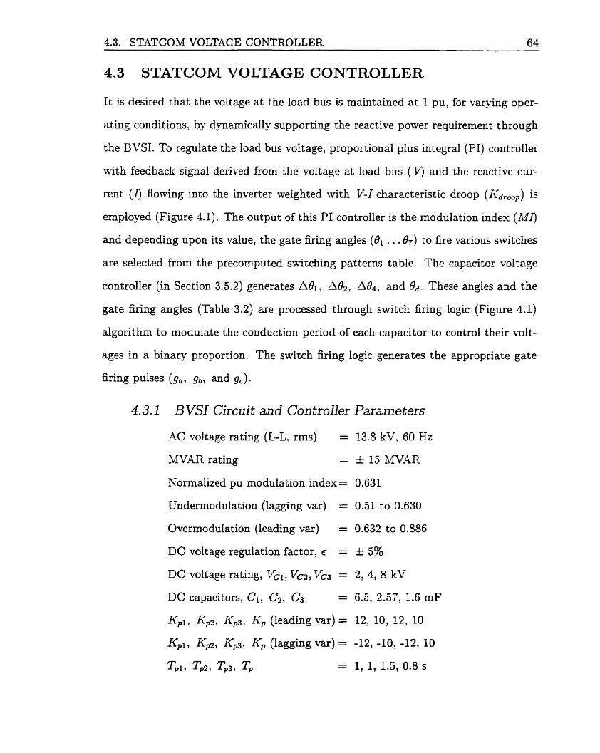
4.3. STATCOM VOLTAGE CONTROLLER 64
4.3 STATCOMVOLTAGE CONTROLLER
It is desired that the voltage at the load bus is maintained at 1 pu, for varying oper-
ating conditions, by d ~ a m i c a l l y supporting the reactive power requirement through
the BVSI. To regulate the load bus voltage, proportional plus integral (PI) controller
with feedback signal deriwd from the voltage at load bus ( V) and the reactive cur-
rent ( I ) flowing into the inverter weighted with V-I characteristic droop (Kdrwp) is
employed (Figure 4.1) . The output of this PI controller is the modulation index (Md
and depending upon its value, the gate finng angles (OL . . . Bi.) to fire various snitches
are selected from the precomputed switching patterns table. The capacitor voltage
controller (in Section 3.5.2) generates ABL, A02, Ad4 and Bd. These angles and the
gate firing angles (Table 3.2) are processed through switch firing logic (Figure 4.1)
algorithm to modulate the conduction period of each capacitor to control their volt-
ages in a binary proportion. The switch firing logic generates the appropriate gate
firing pulses (go , gb 1 and gc) -
4.3.1 B VSI Circuit and Controller Parameters
-4C voltage rating (L-L, rms) = 13.8 kV, 60 Hz
M V ' R rating = & 15 MV-4R
Normalized pu modulation index = 0.631
Undermodulation (lagging var) = 0.51 to 0.630
Overmodulation (leading var) = 0.632 to 0.886
DC voltage regdation factor, É = f 5%
DC voltage rating, V&, Vc2, Va = 2, 4, 8 kV
DC capacitors, Ci, C2, C3 = 6.5, 2.57, 1.6 mF
Kpl, Kp2, Kp3, Kp (leading var) = 12, 10, 12, 10
Kpl, KpZ, KP3, Kp (lagging var) = -12, -10, -12, 10
Tpi7 Tp2 , Tp3? Tp = 1, 1, 1.5, 0.8 s
4.4. TRANSENT SIMULATION 65 - -- - -- .- - - - - - - -
4.3.2 Voltage Controller Parameters
Ku, = 10.0 Zi = L O S
Kdrcop = 1% Kef = 1 . 0 ~ ~
4.4 TRANSIENT SIMULATION
The operation of the blevel BVSI for the dynamic compensation of distribution s -
tem described in Figure 4.1 is evaluated using PSCAD/EMTDC [8] for various distur-
bances and different system operating conditions. The objective of this simulation is
to veri& the effectiveness of the BVSI in reactive power compensation, the suitability
of the capacitor voltage controller (in maintaining the capacitor voltages in binary
proportion) and the voltage controller (in regulating load bus voltage) during selected
severe fault conditions and varied operating conditions.
4.4.1 Switchingfiom Leading to Lagging Mode of Operation
Figure 4.2 illustrates the operation of the BVSI when generating leading vars as well
as absorbing lagging vars. Initially the capacitor voltages are maintained a t 2, 4 and
8 kV levels, the BVSI is in a floating state, and the load bus voltage is 1 pu.
At 0.12 s, 10 MW + j8 MVAR inductive load is added. To maintain the load bus
voltage a t 1 pu, increased capacitive reactive power demand a t the load bus is met
by the inverter. The voltage controller responds to the changed operating condition,
adjusts the modulation index and the inverter generates 11 MVAR capacitive reac-
tive power (Figure 4.2). Figure 4.2 also shows the variations in capacitor voltages
(KI, l&, Vc3), rms load bus and BVSI bus voltages (T/i, V,) , instantaneous load bus
line voltages (va,, ab,, v,). It is seen that after the initial disturbance the capacitor
voltages adjust to the predisturbance binary levels, and is regulated to 1 pu.
At 0.4 s, a 16 MVAR capacitor bank is switched in at the load bus, changing
the load to 10 MW -j 8 MVAR capacitive. It is seen that the inverter is able to
switch from capacitive operation to inductive operation successfully and the load

4.4. TRANSIENT SIMULATION 66
bus voltage is regulated to 1 pu. However, the capacitor voltages are maintained a t
new reduced steady state values, but still in a binary proportion. In principle, the
variation in the dc link voltages does not inherently affect the ability of the inverter to
produce the designated sinusoidal output voltages a t the wanted single synchronous
frequency by appropriately controiling the (instantaneous) magnitude of the inverter's
output voltage [9]. Here too the reduced dc voltages do not affect the effectiveness
of the BVSI in any sense so long as they remain in a binary proportion and are not
reduced substantialiy. if the capacitor voltages drift Erom their binary proportions,
the harmonic distortion would increase.
The line voltage harmonic spectrum is s h o m in Figure 4.2. The total harmonic
distortion (THD) with 60 Hz base frequency and first 100 harmonics considered is
0.3717% at 0.6499 S. The THD values at different time instant are shown in Table 4.1.
These very low THD values indicate that SHEM algorithm with precomputed swîtch-
h g patterns improves the system harmonic profile significantly.
Figure 4.3 illustrates real power flow from ac system into STATCOM to meet its
losses. The real power drawn by STATCOM is very less when there are no distur-
bances. It draws more power to meet increased losses during transient conditions.
This figure also shows AB1,, A&,, and h04, angles used to modulate capacitor switch-
ing periods to regulate their voltages which Vary from -1° to +lO. The ST.4TCOM
bus phase voltages va,, vh, and v, distinctly show 15-steps output.
4.4.2 Three-phase t o Ground Fault at Load Bus
In another test, a five cycles three-phase to ground fault a t the load bus is initiated at
0.35 S. The fault path has zero impedance and at the onset of the fault the load bus
voltage is 1 pu, the BVSI is supplying 11 MVAR leading vars. Resulting waveforms
for this case are illustrated in Figure 4.4. During the fault, the load bus voltage
collapses to O pu, the inverter reaches its limit and the inverter bus voltage drops
up to 0.4 pu. This disturbance causes rapid voltage variations in the dc capacitors

4.4. TRANSIENT SIMULATION 67
as well. Kowever, the capacitor voltage controller is effective in bringing back the
capacitor voltages to their prefault values. After clearing the fault at 0.433 s, the
system is restored back to its predisturbance operating state.
4.4.3 Three-phase t o Ground Fault when STL4TCOM FIoating
Figure 4.5 depicts simulation results for a three-phase to ground fault at the load bus
when the ST.4TCOM is floating. The operating condition is such that the STATCOM
does not need to supply or absorb any reactive power. The ST.4TCOM bus voltage is
equal to the load bus voltage so there is no exchange of reactive power between them.
However, a t the onset of fault, STATCOM swings into action and brings back the
system to its predisturbance operating state irnmediately after clearing the fault. Also
the STATCOM goes into its floating state once the system is restored to normalcy.
4.4.4 Single-phase t o Ground Fault at Load Bus
The transient simulation results for a single-phase to ground a t load bus are shown in
Figure 4.6. The fault path has zero impedance. The load is 8 MW + j10 MVAR. The
BVSI is supplying 11 MVAR leading vars. The results confirm the ability of BVSI
STATCOM to dynamically compensate the system and restore the system to its pre-
fault state once the fault is cleared. The THD is 0.669% and proves the effectiveness
of increased number of steps in the BVSI output and selected harrnonic elimination
algorit hm in minirnizing or eliminating harrnonics intro duced int O the syst em.
4.4.5 Line to Line Fault at Load Bus
The results for a dead short circuit between phase A and phase B at load bus are
illustrated in Figure 4.7. The fault duration is 8 cycles and it is initiated at 0.35 S.
The load is 8 MW + j10 MVAR. The BVSI is supplying about 10 MVAR leading vars.
-4s seen in the previous cases, these resuits and low THD value reinstate the BVSI
STATCOM effectiveness as dynamic compensator Mth low harrnonic distortion.
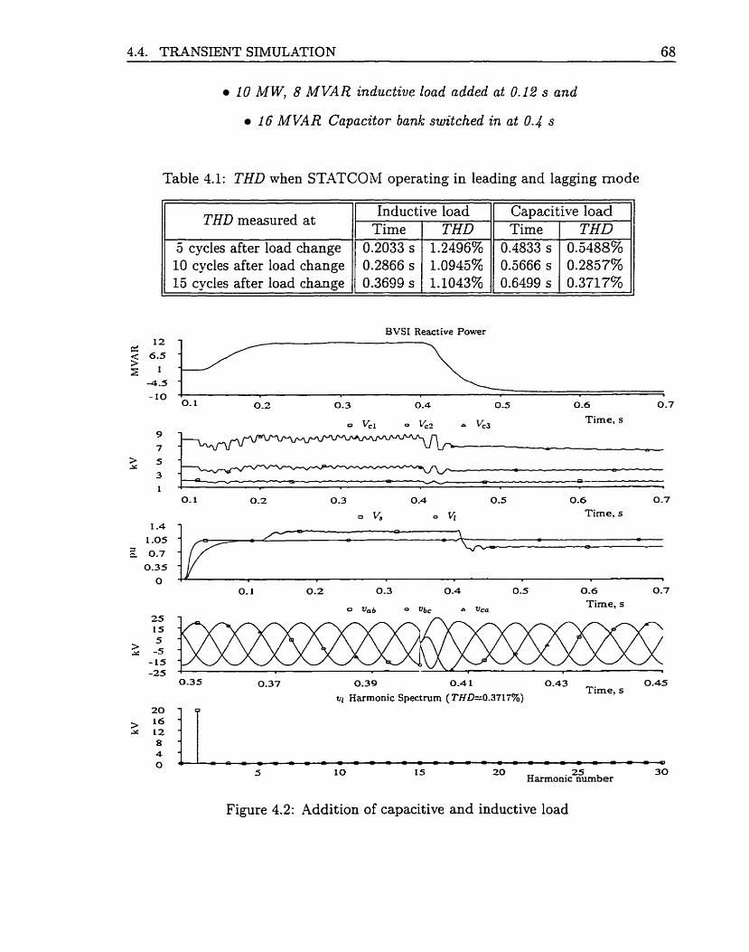
4.4. TRANSENT SIMULATION 68
10 MW, 8 MVAR induct ive load added at 0.12 s a n d
16 MVAR Capaci tor bank switched in at 0.4 s
Table 4.1: THD when ST.4TCOM operating in leading and lagging mode
BVSI Reactive Power
THD measured at
5 cycles after load change 10 cycles after load change 15 cycles after load change
O. 1 0.2 0.3 0.4 0.5 0.6 0.7
a Uca Time, s
a va6 O vbc
0.35 0.37 0.39 0.4 1 0.43 0.45 Time, s
Ur Harmonic Spectrum ( T H l k 0 . 3 7 17%) -
- - - J - 1 0 25 30
20 Harmoaic nurnber
Figure 4.2: Addition of capacitive and inductive load
Inductive Ioad Time
0.2033 s 0.2866 s 0.3699 s
Capacitive load THD
1.2496% 1.0945% 1.1043%
Time 0.4833 s 0.5666 s 0.6499 s
THD 0.5488% 0.2857% 0.3717%

4.4. TRANSIENT SIMULATION 69
BVSI Real Power 7
O. 1 0.2 0 3 0.5 0 5 0.6 0-7 0.8 Time, s
0 Adla 0 A62a A 4fl4a
O. 1 0.2 O3 0.4 0.5 0.6 0-7 0.8 Time, s
0 Vau O ubv A Ucv
1
0.46 0.48 Time, s
Figure 4.3: Typical STATCOM real power consumption
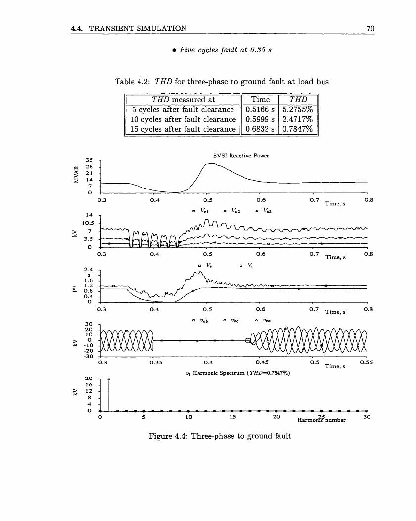
4.4. TRANSIENT SIMULATION 70
Five cycles fault at 0.35 s
Table 4.2: THD for three-phase to ground fault a t load bus
THD measured at 5 cycles after fault clearance 10 cycles after fault clearance 15 cycles after fault clearance
BVSI Reactive Power
-. - -
0.35 0.4 0.45 0.5 0.55 Time, s
vl Harmonic Spectrum (THD=0.7847%)
O 5 1 O 1 5 25 20 Harmon~c nurnber 30
Figure 4.4: Three-phase to ground fault

4.4. TRANSIENT SIMULATION 71
Fzve cycles favlt at 0.35 s
Table 4.3: THD for three-phase to ground fault and ST-4TCOM floating
THD measured at 5 cycles after fault clearance 10 cycles after fault clearance 15 cycles after fault clearance
BVST Reactive Power f
0.7 0-8 Time, s
0.5 0.6
u t ; O vi
0 -7 0.8 Time, s
0.3 0.35 0.4 0.45 0.5 0.55 Time, s
vl Harmonic Spectmm (THD=2.27357%) i 0
O 5 10 15 20 25 30 Harmonic nurnber
Figure 4.5: Three-phase to ground fault when STATCOM floating
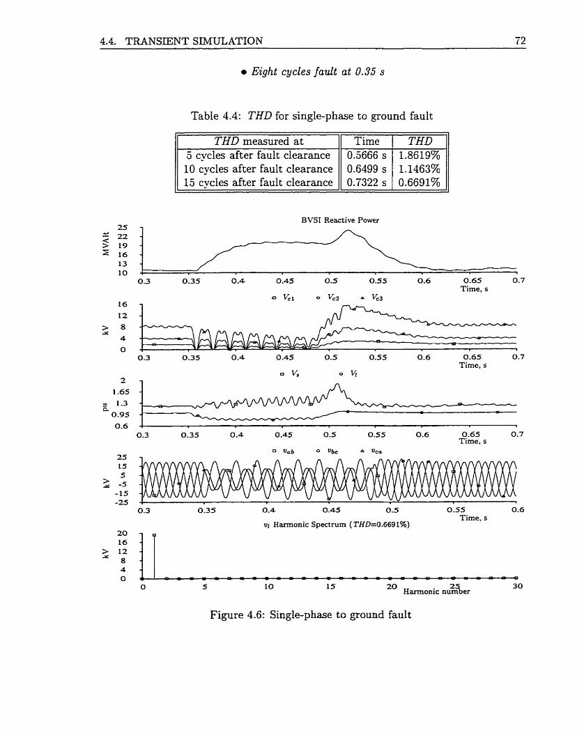
4-4. TRANSIENT SIMULATION 72
Eight cycles fault ut 0.35 s
Table 4.4: THD for single-phase to ground fault
THD measured a t 5 cycles after fault clearance 10 cycles after fault clearance 15 cycles after fault clearance
BVSI Reactive Power -
O -3 0.35 0 -4 0.45 0.5 0.55 0-6 0.65 0.7 Time, s
0 Ki 0 Vc2 a vc3
0.3 0.35 0.4 0.45 0.5 0.55 0.6 0.65 0.7 Time, s
0 v, VI
0.3 0.35 0.4 0.45 0.5 0.55 0.6 9-65 0.7 Time, s
- -
Time, s vl Harmonic Spectrum (THD=0.6691%) -
O 5 IO 1s 20 Harmonic nu%%er
30
Figure 4.6: Single-phase to ground fault

4.4. TRANSIENT SIMULATION 73
Ezght cycles fault at 0- 35 s
Table 4.5: THD for line to line fault
BVSI Reactive Power
1.
THD measured at 5 cycles after fault clearance 10 cycles after fault clearance 15 cycles after fault clearance
-
1
O. 1 0.2 0.3 0.4 0.5 0.6 0-7 0.8 Time, s
0 Ki 0 Vc2 A vc3
0.6 0.7 O. 8 Time, s
0-7 0.8 Time, s
' Time
0.5666 s 0.6499 s 0.7322 s
-- . 0.3 0-35 0 -4 0.45 0.5 O S 5 0.6
Time, s rtl Harrnonic Spectrum (THD=0.9838%)
20 - 16 -
2 12 - 8 - 4 - O O-- -
O 5 1 O 15 20 ~ a n n a n i c n u s e r 30
THD 4.3759% 1.6335% 0.9838%
Figure 4.7: Line t o line fault
4.5. BVSI AS SSSC 74
4.5 BVSI AS SSSC
The application of a 3-level, 16steps binary voltage source inverter as a static syn-
chronous series compensator (SSSC) has been inwstigated in [IO]. The digital simu-
lation performed confirms the applicability of BVSI SSSC to control the real porver
flow on a transmission line in both directions.
4.6 CHAPTER SUMMARY
This chapter presents the digital simulation results of BVSI STATCOM morking un-
der steady state and abnormal operating conditions. Different operating conditions
and wide range of faults are simulated to examine the performance of BVSI STAT-
COM. The results consistently show the low value of THD for al1 the cases validating
the effectiveness of increased number of steps in the stair-case output of BVSI voltage
because of its structure and selected harmonic elimination algorithm in minimizing
or eliminating harrnonics introduced into the system. The BVSI STATCOM can
smoothly switch the operating mode from leading to lagging and vice versa without
jeopardizing its dynamic performance, steady state behavior and harmonic containing
capability. Even when the BVSI is in floating state, and the system experiences an
abnormal condition, it can restore the system to its normal state after the removal
of abnormality and itself goes into floating state again. The simulation results and
low THD value reinstate the BVSI STATCOM usefulness and effectiveness as dy-
namic compensator with very minimum harmonic distortion. The capacitor voltage
controller regulates the capacitor voltages in binary proportion.
BIBLIOGRAPW 75
Bibliography
[l] L. Gyugyi, "Dynamic compensation of ac transmission lines by solid-state syn-
chronous voltage sources," IEEE Transactions on Power Delivery, vol. 9, no. 2,
pp. 904-911, Xpril 1994.
[2] C.W. Edwards: P.R. Nannery, K.E. Mattern, E.J. Stacey, and J. Gubernick,
"Advanced static var generator employing GTO thyristors," IEEE Transactions
on Power Delivery, vol. 3, no. 4, pp. 1622-1627, October 1988.
[3] E. Larsen, N. Miller, S. Nilsson, and S. Lindgren, "Benefits of GTO-baçed compensation systems for electric utility applications," IEEE Transactions on
Power Delivery, vol. 7, no. 4, pp. 2056-2064, October 1992.
[4] T.J.E. Miller, Reactive power control in electric systems, John Wiley & Sons,
1982.
[5] N.G. Hingorani, "High power electronics and flexible ac transmission system,"
IEEE Power Engineering Review, pp. 3-14, July 1988.
[6] Jih-Sheng Lai and Fang Zheng Peng, "Multilevel converter-a new breed of power
converters," IEEE Transations on Industry Applications, vol. 32, no. 3, pp. 509-
517, May/June 1996.
[7] R.W. Menzies and Y. Zhuang, "Advanced static compensation using a multilevel
GTO thyristor inverter," IEEE Transactions on Power Delivery, vol. 10, no. 2, pp. 732-738, April 1995.
[8] Manitoba HVDC Research Center, Winnipeg, Manitoba, Canada,
PSCA D/EMTD C Power Systems Szmul~tion Software, user's manual, 1996.
[9] L. Gyugyi, C.D. Schauder, and K.K. Sen, "Static synchronous series compen-
sator: A solid-state approach to the series compensation of transmission lines,"
IEEE Transations on Power Delivery, vol. 12, no. 1, pp. 406-417, January 1997.
[IO] C.I. Terek, "Application of multilevel binary voltage source inverter as a static
synchronous series compensator," Master's thesis to be submitted to the Depart-
ment of Electrical & Cornputer Engineering, The University of Western Ontario,
London, May 1999.
Chapter 5
LABORATORY PROTOTYPING AND EVALUATION OF BVSI
5.1 INTRODUCTION
The Chapter 3 describes the theoretical deveiopment of multilevel binary voltage
source invert ers (BVSI) . The Chapter 4 illustrates the effectiveness and performance
enhancement of power system when a 3-level, 15-steps BVSI is used as a dynamic
compensator with the help of digital simulation.
This Chapter' presents the design and development of 1 4 , blevel, lbsteps BVSI
laboratory prototype and its microcontroller based digital controller. The design is
described in the folloning stages.
Prototype specifications
Hardware design
Controller design
Cont roller implement ation
Performance analysiç
'A version of this chapter has been submitted for publication. K.V. Patil, J.E. Makaran, J. Jiang, and R.M. Mathur "Experimentai evaiuation of a new multilevel binary voltage source inverter STATCOM as a dynamic compensator", submitted to IEEE Power Engineering Society.

5.2. PROTOTYPE SPECIFICATIONS CC
( (
PROTOTYPE SPECIFICATIONS
r f i 0 0 vars, 1 4 , 120 V, 60 Hz ac, 30/60/120 V dc, 3-level, 15-steps 1
1202 Base 2 = - = 36 !2
400
Interface reactor = 12 mH
Source impedance = 180 mH
28 Vdc M I AC voltage output, Vph = = 6.3022 Vd, M I
I h
DC voltage input, Vdc = 120
= 30.22 = 30 V for M I = 0.63 6.3022 MI
DC source capacitors
For &II = MI,,, = 0.81
O1 = 5.423", O2 = 13.322", O3 = 19.305", O4 = 27.04g0, O5 = 37.093',
O6 = 31.917°, O7 = 63.093' and Voltage regdation factor E = 0.056 pu
Ci = [l - sin O1 + sin O2 - sin e3 + sin Bq - sin û5 + sin Os - sin û7] 2 w E Vdc
C2 = [l - sin O2 + sin B4 - sin Os] 4 w E Vdc
c3 = A I
[l - sin 04] 8 u E VdC
A picture of the prototype is shown in Figure 5.1.

5.2. PROTOTYPE SPECIFICATIONS 78
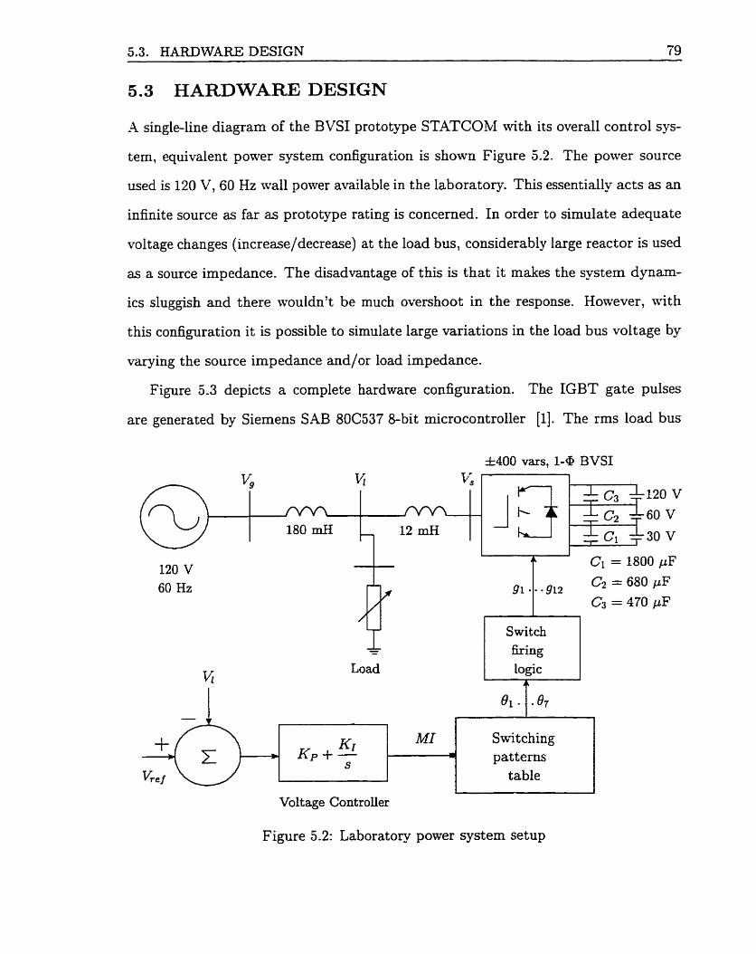
5.3. HARDWARE DESIGN 79
5.3 HARDWARE DESIGN
A single-line diagram of the BVSI prototype STATCOM with its overall control sys-
tem, equivalent power system configuration is shown Figure 5.2. The power source
used is 120 V, 60 Hz mal1 power availabIe in the laboratory. This essentially acts as an
infinite source as far a s prototype rating is concerned. In order to simulate adequate
voltage changes (increase/decrease) at the load bus, considerably large reactor is used
as a source impedance. The disadvantage of this is that it makes the system dynam-
ics sluggish and there wouldn't be much overshoot in the response. However, with
this configuration it is possible to simulate large variations in the load bus voltage by
varying the source impedance and/or load impedance.
Figure 5.3 depicts a complete hardware configuration. The IGBT gate pulses
are generated by Siemens S.4B 80C537 8-bit microcontroller [l]. The rms load bus
t Load
3~400 vars, 1-@ BVSI 1
Switch firing
Voltage ControlIer
Figure 5.2: Laboratory power system setup
Kr b K p + -
S
Kef patterns
table
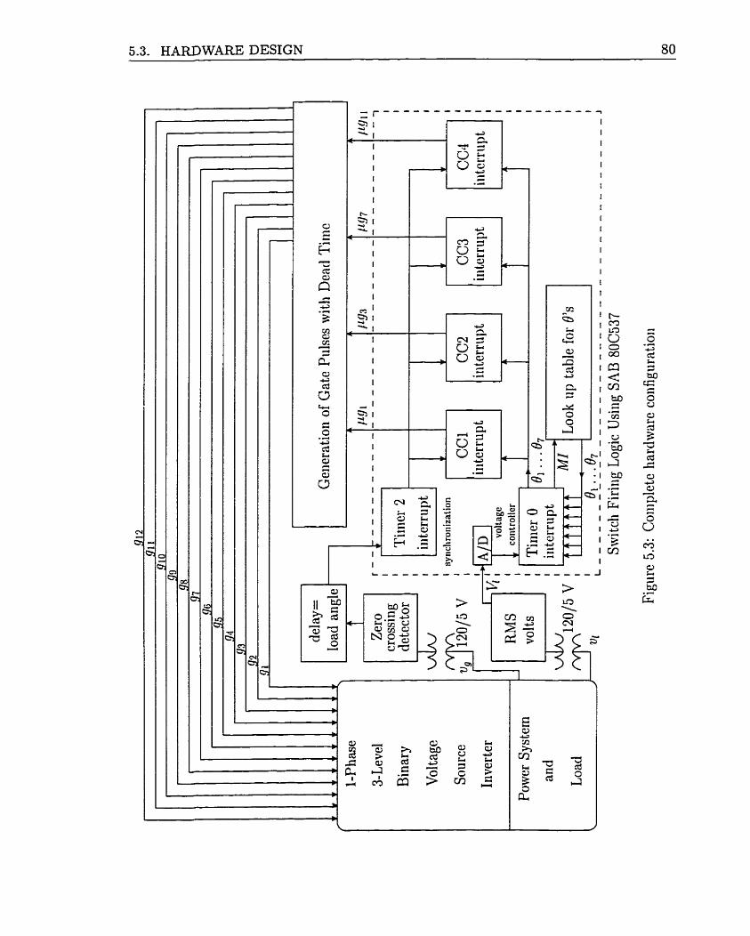
5.3. HARDWARE DESIGN 80
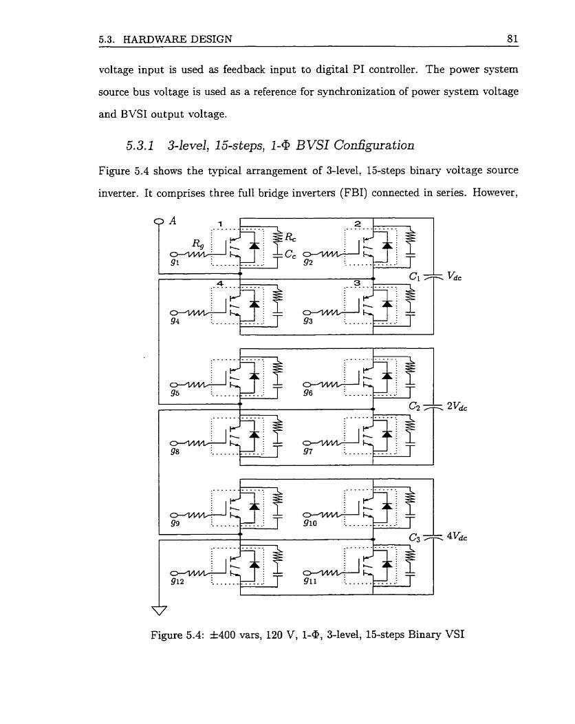
5.3. HARDWARE DESIGN 81
voltage input is used as feedback input to digital PI controller. The power system
source bus voltage is used as a reference for synchronization of power system voltage
and BVSI output voltage.
5.3.1 blevel, 15-steps, 1-<P B VSI Configuration
Figure 5 -4 shows the typical arrangement of 3-level, 15-steps binary voltage source
inverter. It comprises three full bridge inverters (FBI) connected in series. However,
Figure 5.4: &400 vars, 120 V, 1 4 , blevel, 15-steps Binary VSI

5.3. HARDWARE DESIGN 82
their dc voltage inputs are arranged in binary proportion as 30: 60: and 120 V dc
for the prototype developed. The figure shows the IGBT as switching elements with
ant i-parallel diodes.
Figure 5.5 shows the realization of one FBI using Powerex ~ntellimod*" Intelligent
Power Module (IPbl) [2]. The IPM used in the prototype is PM1SCSJ060. The
IPMs are advanced hybrid power devices that combine high speed, low loss IGBTs
with optimized gate drive and protection circuitry. These IPMs have sophisticated
built-in short circuit, over current, over temperature and under voltage protection
circuits which improve their reliability and specially designed, optimized gate drive
circuits eliminate the need for a negative supply to off bias the IGBT. Figure 5.5 also
illustrat es the interface of IPM with the optocoupled transistor circuits for control
(HCPL 4503) and fault output (PC817). The common emitter amplifier stage (using
ZN 3904) is introduced between microcontroller gate output signais and control circuit
optocoupler transistor inputs to amplify the power of gate signals in order to be able
to drive the required number of IGBTs simultaneously. It is to be noted that the
IPM has six switches configured in 6-pulse manner. But only four switches are used
and remaining two are always held in off-state to configure the IPM as FBI.
5.3.2 BVSI Controller
Figure 5.6 shows the detailed circuit diagram of an SAB 80C537 with external pro-
gram memory represented by 256 Kbytes 27C256 ensable, electrically programmable
read-only rnemory (E2PROM) and 74LS373 three-state D-latch for address decoding.
This diagram also shows the basic power supply connections. The TLEX260 is used
to supply a positive constant 5.0 V dc voltage to the microcontroller. The inputs to
the microcontroller are rms load bus voltage and negative transition source voltage
zero crossing signal for synchronization. The outputs from the rnicrocontroller are
pgi, ~ 9 3 ~ pg7, and pg,,. The 12 MHz crystal provides the clock signal.
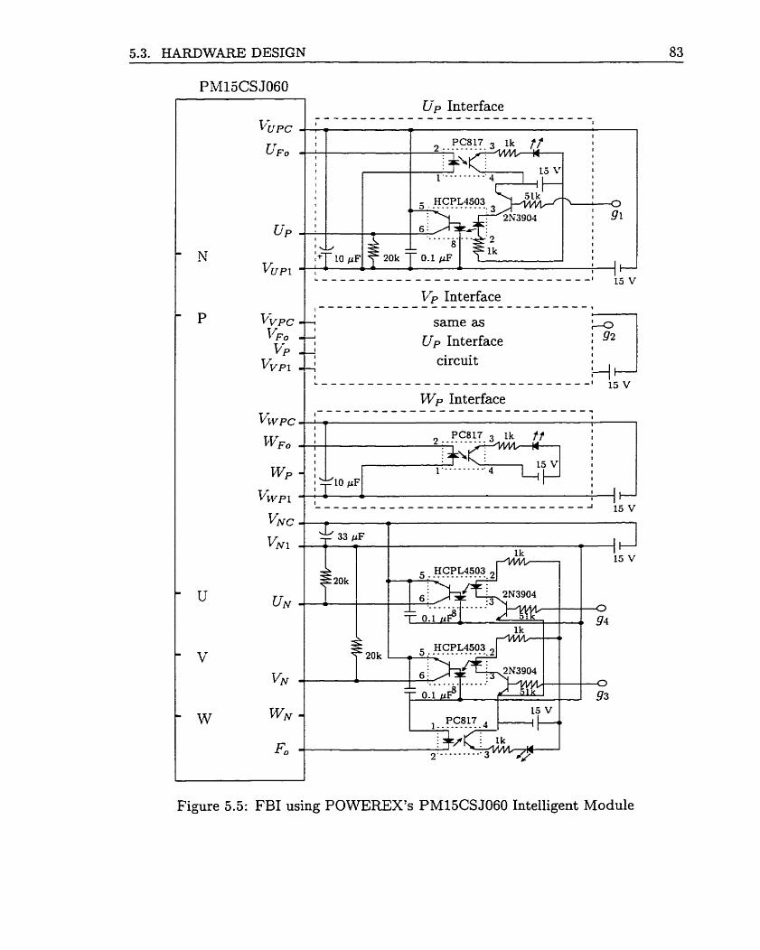
5.3. HARDWARE DESIGN 83
sarne as U p Interface
Figure 5.5: FBI using POWEREX's PM15CS JO60 Intelligent Module

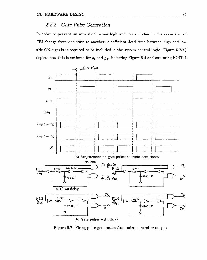
5.3. HARDWARE DESIGN 85
5.3.3 Gate Pulse Generation
In order to prevent an arm shoot when high and low switches in the same arm of
FBI change from one state to another, a sufficient dead time between high and low
side ON signals is required to be included in the system control logic. Figure 5.7(a)
depicts how this is achieved for gl and 9,. Referring Figure 5.4 and assuming IGBT 1
(a) Requirement on gate pulses to avoid arrn shoot
(b) Gate pulses with delay
Figure 5.7: Firing pulse generation from microcontroller output
5.3. HARDWARE DESIGN 86
is conducting and IGBT 4 is non conducting, then a t the instant when IGBT 1 needs
to be turned-off and IGBT
then after delay time of dl
gate signal pgl is available.
be derived.
4 needs to be turned-on, IGBT 1 is switched-off first and
= 10ps IGBT 4 is switched-on. From
From this signal other signals shown in
microcontroller a
Figure %'(a) can
Let, -4 = ~ 9 1
B = m(t - d t )
A careful observation of the Figure 5.7(a) tells that,
X = A B + A B = 4 CB B
91 = X A = ( A B + A B ) A = AB = pgl pg,(t -dt)
g,=x B = (AB + AB)B = A B = m a ( t - d , )
Figure 5.7(b) describes the implementation of above logic to realize 12 gate pulses
(gl . . . gI2) from 4 microcontroller output gate signals (mi, pg3, p g ~ , and pgll). The
lOps delay is obtained by RC circuit as shown.
5.3.4 RMS Load Bus Voltage as Input to PI Controller
Figure 5.8 shows the circuit used to measure rms load bus voltage using RMS-to-dc
converter AD637 which computes the true rms value of any complex waveform. The
capacitor Ca, = 1 pF is selected to reduce the averaging error as well as to optirnize
the settling time. To reduce the ripples further a two pole Sallen-Key Filter (24K
and 3.3 pF) is used. In order to electrically isolate the high voltage ac ground from
the low voltage dc ground, a step down transformer is used.
5.3.5 Synchr~~zation of Power System and BVSI
An LM339 comparator is used as a zero crossing detector of the source voltage as
shown in Figure 5.9. This signal provides interrupt request to Timer 2, External
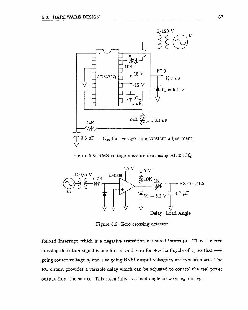
5.3. HARDWARE DESIGN 87
T 3.3 PF Ca" for average time constant adjustment
Figure 5.8: REiIS voltage measurement using AD637JQ
* * DeIay=Load Angle
Figure 5.9: Zero crossing detector
Reload Interrupt which is a negative transition activated interrupt. Thus the zero
crossing detection signal is one for -ve and zero for +ve half-cycle of v, so that +ve
going source voltage u, and +ve going BVSI output voltage v, are synchronized. The
RC circuit provides a variable delay which can be adjusted to control the real power
output from the source. This essentially is a load angle between v, and vl.

5.4. CONTROLLER DESIGN 88
5.3.6 +15 V Regulated DC Supply for Gate Drive Circuits
The six-pack IPM PMl5CSJ060 requires four (three for three hi& side switches and
one for three low side switches) isolated ponrer supplies for their gate drive and pro-
tection circuits. Figure 5.10 shows one power supply circuit using LM317 regulator.
5.4 CONTROLLER DESIGN
5.4.1 Voltage Controller
The voltage controller is implemented in microcontroller in the form of a digital PI
controller. The general continuous time PI controller is defined by
Using bilinear transformation to convert analog PI into discrete domain (trapezoidal
integration)
Figure 5.10: Regulated +15 V dc supply
IN4148 I I n
IN4002 --A( ~ ~ 3 1 ' 1 4
-3 f\ 15 V -3
120/20 v 470 pF & 10 pl? 25 p ~ "
AI electrolytic - Al elect rolytic Al electrolytic
K d j
== 0.1 pF disc
240 R
2.7k -+ /-\
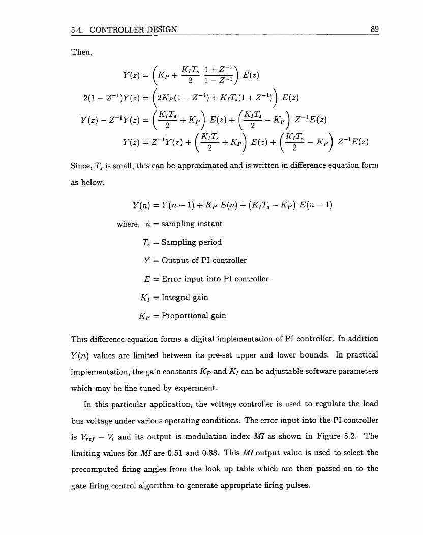
5.4. CONTROLLER DESIGN 89
Then,
Since, Ts is small, this can be approximated and is written in difference equation form
as below.
where, n = sampling instant
Ts = Sampling period
Y = Output of PI controller
E = Error input into PI controller
KI = Integral gain
Kp = Proportional gain
This difference equation forms a digital implementation of PI controller. In addition
Y(n) values are limited between its pre-set upper and lower bounds. In practical
implementation, the gain constants Kp and KI can be adjustable software paramet ers
which may be fine tuned by experiment.
In this particular application, the voltage controller is used to regulate the load
bus voltage under various operating conditions. The error input into the PI controller
is Vrej - and its output is modulation index MI as shown in Figure 5.2. The
limiting values for MI are 0.51 and 0.88. This MI output value is used to select the
precomputed firing angles from the look up table which are then passed on to the
gate firing control algorithm to generate appropriate firing pulses.
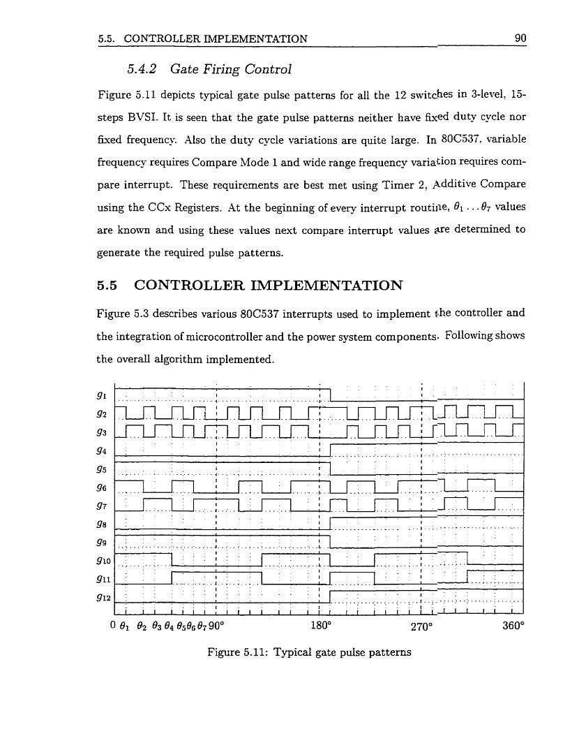
5.5. CONTROLLER IMPLEMENTATION 90
5.4.2 Gate Firing Control
Figure 5-11 depicts typical gate pulse patterns for al1 the 12 switcbes in 3-level: 15-
steps BVSI. It is seen that the gate pulse patterns neither have d u t ~ cycle nor
k e d frequency. Also the duty cycle variations are quite large. In 8063.37. variable
frequency requires Compare Mode 1 and wide
pare interrupt- These requirements are best
using the CCx Registers. At the beginning of every interrupt routiile,
are known and using these values next compare internipt values
generate the required pulse patterns.
O1 ... O7 values
determined to
5.5 CONTROLLER IMPLEMENTATION
Figure 5.3 describes various 80C537 interrupts used to implement fhe controller and
the integation of microcontroller and the power system components~ Following shows
the overall algorithm implemented.
Figure 5.11: Typicd gate pulse patterns
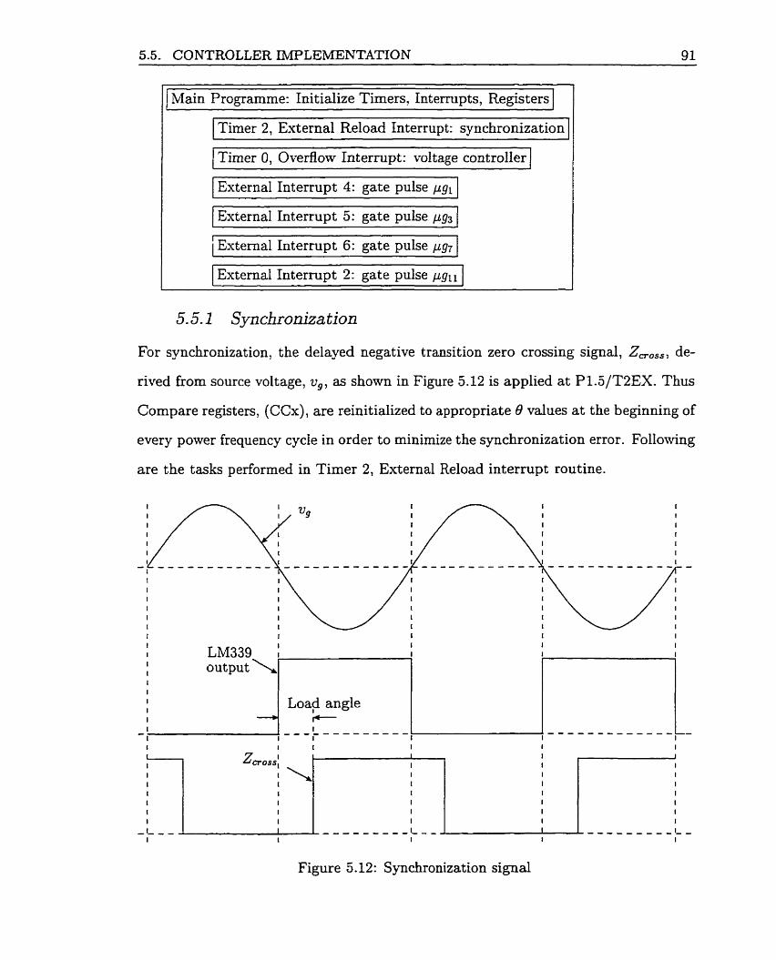
5.5. CONTROLLER IMPLEMENTATLON 91
[Main Programme: Initialize Timers, Intempts, Registers 1 ) Timer 2, External Reload Interrupt: synchronization 1 1 Timer O, Overfiow Interrupt: voltage controller 1 1 External Interrupt 4: gate pulse pglI
1 External Interrupt 5: gate pulse pg3 1 / External Interrupt 6: gate pulse pg7 1 / External Interrupt 2: gate pulse pgll 1
L
For synchronization, the delayed negative transition zero crossing signal, Z,,,,, de-
rived from source voltage, v,, as shown in Figure 5.12 is applied at P1.5/T2EX. Thus
Compare registers, (CCx), are reinitialized to appropriate û values a t the beginning of
every power frequency cycle in order to minimize the synchronization error. Following
are the tasks performed in Timer 2, External Reload interrupt routine.
Figure 5.12: Synchronization signal
5.5. CONTROLLER IMPLEMENTATION 92
Timer 2, External Reload Interrupt
- Clear EXF2
- Assign CC1=180°: CC2=O1, CC3=02, CC4=04
- If first time after startlreset, start Timer O and Timer 2
5.5.2 A/D Conversion of RMS Load Bus Voltage
From the equations (3.18)and (3.20)
derived in Chapter 3, the relation between BVSI ac voltage output and MI for the
prototype developed can be obtained as belon..
Modulation Index, MI, is lirnited between 0.51 to 0.88. Corresponding to these limits,
ac voltage outputs from the BVSI are 97.1448 V and 167.6224 V. In 80C537 .4/D
converter, it is possible to adjust the internal reference voltages through software to
increase the resolution. The internal reference voltages are set to VrnrAcNo = 2.1873
and VIntAREF = 5.0 V. The resulting scaled voltages are digitized in 8-bit form.
5.5.3 Digital PI Controller
In 80C537, the digital voltage controller is implemented using Timer O, Ovedow
interrupt. The tasks performed in the PI algorithm are the following.

5.6. PERFORMANCE VECRIFICATION 93
Timer O, Overflow Interrupt
- Read A/D converter
- Error = V;ef - Vi
- Check region of operation
Error < O, Inductive; Error > O, Capacitive; Error = O, Exit
- MI = M l ( n - 1) + KpError(n) + (TsKr - Kp)Error(n - 1)
- Check MI limits
- Caiculat e new look up table location pointer
- Reassign Timer O registers (THO, TLO)
5.5.4 Ga t e Firing Control
The IGBT gate firing logic is implemented in Timer 2, Compare Mode 1, Com-
pare/External Interrupts 4, 5, 6 , and 2. Task schedule for these additive compare
interrupt routines is as below.
Compare/External Interrupts 4, 5, 6 , 2
- Save current status
- Calculate CCx increment (addition)
- Reload CCx with CCx(n+l)=CCx(n)+ CCx increment
- Complement port latchs P1.1, P1.2, P1.3, P1.4
- Restore old status
5.6 PERFOWANCE VERIFICATION
Figure 5.13 depicts a more explicit representation of the ac system configuration
which simulates various abnormal electric power system conditions to study the BVSI
transient and dynamic performance. It also shows the measurement circuit. The RLC
load is formed by 118 R resistor, 60 mH inductor, and 32 pF capacitor. The potential
dividers (using 150K, 10K resistors) are used to scale down the bus voltages that
can be measured on Yokogama AR1200 Analyzing Recorder. The bus voltages are

5.6. PERFORMANCE VERIFIC ATION 94
Load
Figure S. 13: Simulation setup
isolated and stepped down from high voltage ac side using transformers. The electrical
isolation from high voltage ac side helps in reducing the ground noise and switching
noise entering into the controller circuit.
5.6.1 Overview of Study Cases
A number of abnormal conditions are simulated to demonstrate the transient and
dynamic performance of BVSI ST.4TCOM. The cases studied include:
When BVSI not operating a t the time of load change
Case 1- Switching in resistive (R) load, Figure 5.14
Case 2- Switching in inductive (L) load, Figure 5.15
Case 3- Switching in capacitive (C) load, Figure 5.16
Case 4 Switching in FU loads, Figure 5.17
Case 5- Switching in RC loads, Figure 5.18
Case 6- Switching in LC loads, Figure 5.19
5.6. PERFORMANCE VERZFICATION 95
Case 7- Switching in RLC loads, Figure 5.20
0 When BVSI operating at the time of load change
Case 8- R/L loads connected, switching in R/L/C loads, Figure 5.21
Case 9- RL/RC/LC loads connected, switching out R/L/C loads, Figure 5.22
Case 10- RLC loads connected, switching out R/L/C loads, Figure 5.23
5.6.2 Discussion of Results
Figures 5.14 to 5.20 show the rms generator bus voltage 1.5, load bus voltage I/{:
and STATCOM bus voltage V,, the instantaneous voltages of these buses (v,, vl, v,
respectively), and the harmonic spectrum of load bus voltage. Figures 5.21 to 5.23
show V,, &, and, V,. The 1 pu voltage is 125 V. All the results show the ability of
BVSI STATCOM to dynamically regulate the load bus voltage.
As shown in Figure 5.14, initially there is no load and STATCOM is disconnected
from the system (switch S, is open), but its voltage controller is enabled. There is
veq- small leakage current (due to measurernent circuit) flowing in the circuit and
because of large source inductance the open circuit load bus voltage and ST.4TCOM
bus voltages are slightly less than 1 pu. When the resistive load is added to the system
and ST.4TCOM is still disconnected from the system, & and V, drop to about 0.73
pu. Immediately after the connection (switch S, is closed), STATCOM brings back
the load bus voltage to 1 pu by supplying required capacitive vars. The STA4TCOM
bus voltage is about 1.15 pu.
Figure 5.14 also shows the instantaneous generator bus voltage vg and load bus
voltage vi when STATCOM, resistive load are connected. The output voltage of
STATCOM and hence the load bus voltage are synchronized wïth generator bus
voltage assuming a phase lag of 40". Normally one should interactively calculate the
phase angle between vg and vl which depends on the load value. The BVSI and rest

5.6- PERFORMANCE VERIFICATION 96
of the system are then synchronized for this phase angle difference. The ui waveform
distinctly shows the 15-steps output of STATCOEVI.
The third part in the figure illustrate the harmonic spectrum of the load bus
voltage upto 30 harrnonics. The fundamental voltage is &=129.57 V=1.036 pu,
THD=15.46% with al1 h m o n i c s coosidered and THD=2.15% when 3rd and its mul-
tiple harmonics are neglected which would be the case of 3-4 system. The prototype
studied here is 1 4 , so its output voltage contains 3rd and its multiple harmonics.
These results show the ability of BVSI STATCOM to regulate the load bus voltage
and effectiveness of selected harmonics elimination algorithm implemented in reduc-
ing the harmonics introduced in the system.
The BVSI STATCOM performance for inductive load is shown in Figure 5.15. It
is observed that the load voltage drops to about 0.55 pu, and to bring this voltage
back to 1 pu, STATCOM should act more capacitive than in the case of resistive load.
This is evident from the figure, Vs=1.22 pu as compared Vs=l.15 pu in the case of
resistive load. Here again the STrZSCOM is able to brhg back the load bus voltage
to 1 pu and the total harmonic distortion is 2.99%.
The BVSI STATCOM performance for capacitive load is illustrated in Figure 5.16.
The feedback controller input to rnicrocontroller is clipped to 5 V, that's why
the I/i shown in the figure is clipped to about 1.5 pu. Actually this voltage rise is
about 2.5 pu. As is required, after the connection STA4TCOM acts as reactive power
absorber, pulling down the load bus voltage and dynamically adjusting its reactive
power absorption to regulate the load bus voltage to 1 pu. The ST-4TCOM bus voltage
is about 0.8 pu. The 2nd part of the figure shows u,, ul and us. The us waveform
shows 15-steps. The vl harmonic spectrum shows the excessive 3rd harmonic content,
however the THD is 2.66% excluding 3,6,9. . . harmonics.
Fi y r e s 5.17 to 5.20 lead to similar observations of effectiveness of BVSI STAT-
COM in regulating the load bus voltage.

5.6. PERFORMANCE VEFUFICATION 97 -- - -
Figures 5.21 to 5.23 show the ability of BVSI ST-4TCOM to dynamically adjust its
reactive power generation/absorption to regulate the load bus voltage to 1 pu. Figures
show that there is not much variations in the load bus voltage when new load is added
or disconnected from the system. They confirm the ability of STATCOM to change
from capacitive to inductive mode of operation and vice versa when demanded by
system operating condition. The harmonics introduced by the inverter is minimized
and is well within the accepted limits.
No Load 1-5 1 BVSI Floating
R Load BVSI Floating
R Load BVSI Connected
0.5 ! I I I I I I L
O i
0.5 1 1.5 2 2.5 3 3.5 4 Time, s
t 1 1 1 1 1 1 I 1
3.96 3.965 3.97 3.975 3.985 3.99 3.995 4 +Ee , s
129.57 vr Harmonic Spectrum
THD= 15.46% THD= 2.15% excluding 3 , 6 , 9 . . .
50
o ! ! i ! & ~ l l l ~ , i l l l l , ~ l l l l l l t i l I ~ I i O 5 10 15 20 25 30
Harmonic number
Figure 5.14: Case 1- BVSI floating, switching in R load
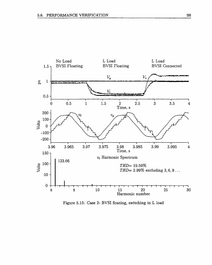
5.6. PERFORMANCE VERIFICATION 98
No Load 1.5, BVSI Floating
L Load BVSI Floating
L Load BVSI Connected
I 1 1 1 I 1 1 i 1
O 0.5 1 1.5 2 2.5 3 3.5 4 Time, s
1 1 I I
3.975 3.98 3.985 Time, s
15 20 Harmonic number
100 -
50 -
O
Figure 5.15: Case 2- BVSI floating, switching in L load
vl Karmonic Spectrum 123.66
THD= 19.59% THD= 2.99% excluding 3,6,9 . . .
1 I I i i i i i ; i i i i r i i i i i l i I 1 l I I I I I 1

5.6. PERFORMANCE VERIFICATION 99
C Load BVSI Connected
No Load C Load BVSI Floating BVSI Floating - v-
- - - K
v, I I 1 I I I i 1
Time, s
O 5 10 15 20 25 30 Harmonic number
3.96 3.965 3.97 3.975 3.98 3.985 3.99 3.995 4
150 - Time, s
ul Harmonic Spectrum
Figure 5.16: Case 3- BVSI floating, switching in C load
* 100 - - 3
50 -
118.69 THD= 41.28% THD= 4.87% excluding 3,6,9. . .
O I I l l l l l l l l i i l l l l l l
B I I 1 1 I l I I I I 1 1 1

5.6. PERFORMANCE VEFUFICATION 100
Xo Load R Load RL Load BVSI Floating
RL Load BVSI Connected
Time, s - ul Barmonic Spectrum
122.64 - THD= 14.35% THD= 3.49% excluding 3,6,9 . . . -
I I ~ I I 1 1 1 1 1 1 1 1 1 1 1 1 1 1 1 1 1 1 l l l ~ l ~ ~
I
15 20 Harmonic number
Figure 5.17: Case 4 BVSI floating, switching in RL loads
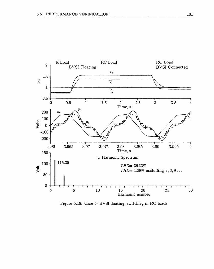
5.6. PERFORMANCE VERIFICATION 101
R Load RC Load BVSI Floating
K
RC Load BVSI Connected
2 2.5 3 Time, s
I I 1 L 1 1 1 1
3.96 3.965 3.97 3.975 3.98 3.985 3.99 3.995
150 1 Time, s
Y Harmonic Spectrum
100- 113.35 THD= 39.83% THD= 1.39% excluding 3,6,9.. .
I 1 1 l 1 I I t I I I 1 I I 1 1 I 1 1 1 I I I I I I t œ
15 20 Harrnonic number
Figure 5.18: Case 5- BVSI floating, switching in RC loads

5.6. PERFORMANCE VERiFICATION 102
No Load L Load LC Load
1 BVSI Floating LC Load BVSI Connected
O 0.5 1 1 .5 2 2.5 3 3.5 4 Time, s
3.96 3.965 3.97 3.975 3.98 3.985 3.99 3.995 4 Time, s
IEio 1 ul Harmonic Spectrum
m 100 - 119.44 4 ri.( THD= 42.43% 9 THD= 2.66% excluding 3,6,9 . . .
1 1 1 1 1 1 1 1 1 1 1 1 1 1 1 ~ 1 ~ ~ 1 l l l l l l t
0 5 10 15 20 25 30 Harmonic number
Figure 5.19: Case 6- BVSI floating, switching in LC loads

5.6. PERFORMANCE VEFUFICATION 103
No Load R Load RL Load RLC Load RLC Load
l - j i BVSI Floating BVSI Connected
O 0.5 1 1.5 2 2.5 3 3.5 4 Time, s
200 -
m & 100 -
- 0 - 9 -100 - -200 -
1 1 1 I I 1 1 i
3.96 3.965 3.97 3.975 3.98 3.985 3.99 3.995 4
150 - Time, s
Harrnonic Spectrum
100 - 118.49 4 2 + THD= 33.93% 9 THD= 2.56% escluding 3,6,9 . . .
50 -
~ ~ I ~ I I I I I I I ~ ~ I I I I I ~ 1 I I 1 I I 1 i
0 5 10 15 20 25 30 Harrnonic number
Figure 5.20: Case 7- BVSI floating, switching in RLC Ioads

5.6. PERFORMANCE VEFüFICATION 104
1 R Load K \
RL Load
1 R Load V'\ RC Load
L Load - RL Load
I
4
-
L Load LC Load
0.4 0.6 0.8 1 1.2 Time, s
Figure 5.21: Case 8- BVSI, R/L loads connected, switching in R/L/C loads
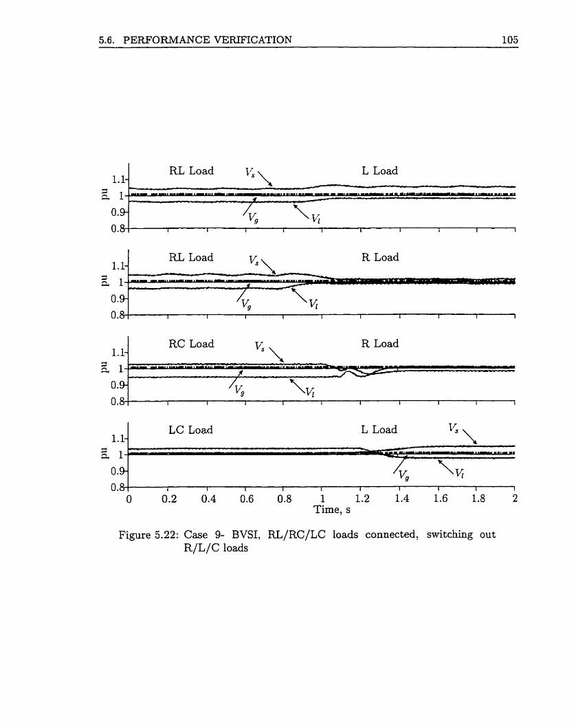
5.6. PERFORMANCE VERIFICATION 105
L Load
l
FU Load R Load
RC Load R Load
LC Load L Load 1.1-
O.%
0.8 =b
t 1 1 1 I 1 I 1 I 1
O 0.2 0.4 0.6 0.8 1 1.2 1.4 1.6 1.8 2 Time, s
Figure 5.22: Case 9- BVSI, RL/RC/LC loads connected, switching out R/L/C loads
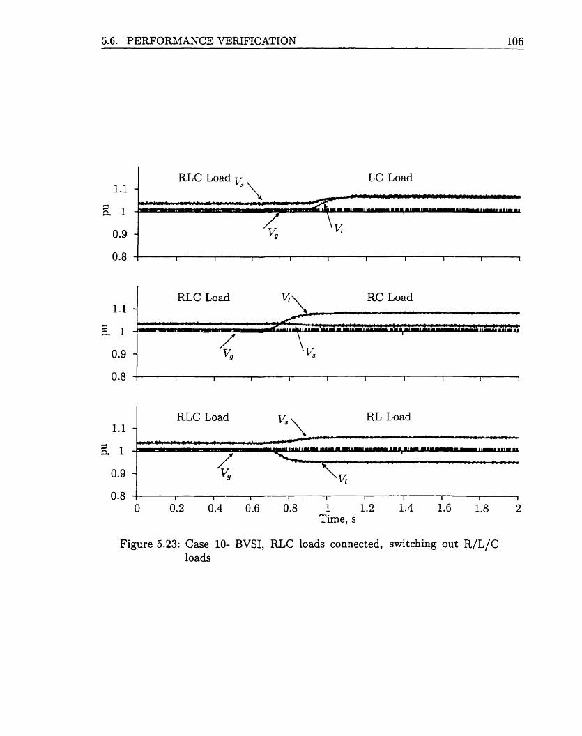
5.6. PERFORMANCE VERlFICATION 106
I RLC Load K , LC Load
RLC Load RC Load
1 RLC Load RL Load
Figure 5.23: Case 10- BVSI, RLC loads connected, switching out R/L/C loads

5.7. HARDWARE LIMITATIONS 107
5.7 HARDWARE LIMITATIONS
The SAB 80C537 microcontroller used is &bitl external 256K E2PROM, 12 MHz
clock device. The main tasks needed to be performed in it were:
Synchronization
Digital PI voltage controller
Capacitor voltage controller
Gate pulses generation algorithms with dead time
a Look u p table of firing angles for various modulation indexes
Due to microcontroller CPU speed (1 machine cycle=l ps) and the memory size
it was not possible to implement a11 the above tasks. The minimum required tasks
needed to qualitatively examine the BVSI performance were irnplemented. They
include:
Synchronization. The algorithm takes 56 ps.
Digital PI voltage controller. The algorithm takes 122 p.
Four gate pulse generation algorithms for g,, g3, g ~ , and gl,. Each algorithm
works in parallel and takes from 40 ps to 75 p i .
Look up table of firing angles for various modulation indexes. Modulation
indexes from 0.51 to 0.88 in steps of 0.1 and corresponding angles are imple-
rnented. The maximum time gate pulse algorithm takes is 75 ps = 1-62'. This
puts restrictions on the firing angles, O1 . . . & values. There must be a minimum
difference of more than 1-62" between any two sequential 9 values.
5.8. CHAPTER SUMMARY 108
There were no filters used on the feedback signal 14. Only a 0.1 pF capacitor was
used to filter the switching noise. It would be prudent to use a high pass filter to
filter out the noise and improve the acciiracy of controller.
The prototype development would be better, easier and speedier if high speed DSP
board with enough I/O is used. Then it d l be possible to implement the capacitor
voltage controller as well. It might be possible for rms voltage calculation, dead time
and gate pulse generation in DSP reducing number of auxiliary hardware components
used in this development.
5.8 CHAPTER SUMMARY
This Chapter describes complete hardware and software design and development of
1 4 , blevel, Ibsteps binary voltage source inverter prototype. The BVSI is then
studied for its effectiveness and capability to work as static synchronous compensator
in an electrical power system to dynamically regulate the Ioad bus voltage.
The results show that BVSI is able to regulate the load bus voltage even during
large abnormal operating conditions by supplying/absorbing adequate amount of re-
active power. The STATCOM transition frorn capacitive reactive power generation
mode to inductive reactive power absorption mode and vice versa as demanded by the
system is smooth. The power quality degradation caused by harmonic introduction
is within the accepted limits proving the efficacy of selected harrnonic elimination
technique employed.

Bibliography
[l] Siemens, Microcomputer Components, SAB 8OCSl7/8OC537, &Bit CMOS Single- Chzp Mzcrocontroller.
[2] Powerex, IGBTMOD and 1ntellimo8"- Intelligent Power Modules, Applications
and Data Book.

Chapter 6
EPILOGUE
6.1 CONCLUSIONS
The imminent deregulation of electrical energy utilities is forcing them to look for
different means and ways to optirnize and control their power transmission networks.
Advanced power electronic devices and Flexible .4C Transmission Systems (FACTS)
technologies [l, 21 are providing the required solutions. A STATCOM is one type
of power electronic equipment emerging under the aegis of FACTS devices for such
purposes [3, 4, 51. The STATCOM typically negotiates reactive power in shunt at the
point of common coupling thereby allowing automatic regdation of that bus voltage
and influences the voltage profile of power system in the vicinity.
The core of this thesis is the investigation of various feasible applications of ST.4T-
COM in an electrical power system to improve its dynamic performance. Also, a new
multilevel binary voltage source inverter (BVSI) configuration is proposed and t ested.
Using this BVSI, a ST.4TCOM with controllable and harmonically minimized output
voltage can be built.
The application of STATCOM for darnping of the torsional oscillations that occur
in a series cornpensated ac system is examined in the IEEE first benchmark sys-
tem [6]. The results from the analflical and digital simulation studies reveal that a
STATCOM with PI controller to regulate the bus voltage, along with an auxiliary

6 -1. CONCLUSIONS 111
signal derived from the generator speed deviations can suppress the unstable torsional
mode oscillations.
A new multilevel binary voltage source inverter mith separate dc sources is intro-
duced. The dc voltages are staggered and controlled in binary proportion of LLC, 2Vdc,
4Vdc, etc., where I/d, is chosen to get the desired ac voltage output. This n-level BVSI
produces a (2"+' - 1)-steps ac voltage output with n full bridge inverters connected
in series. The increased number of steps in the ac voltage of this inverter result into
nearly sinusoidal ac voltage output. Furt her , employing selective harrnonic elimina-
tion modulation technique to eit her completely eliminate or minirnize the harmonics,
the total harrnonic distortion can be kept within acceptable limits.
Application of a BVSI STATCOM for dynamic compensation of 13.8 kV distri-
bution system is exarnined through transient studies. A laboratory prototype of 400
vars, 120 V, 1 4 , 3-level, 15-steps binary voltage source inverter is implemented. A
digital controller using Siemens SAB 80C537 &bit microcontroller is developed for
this prototype.
The results from digital simulation and hardware implementation show the effec-
tiveness of BVSI ST.4TCOM as a dynamic compensator under a wide range of steady
state and abnormal operating conditions. The low value of total harmonic distor-
tion validates the effectiveness of BVSI structure and selected harmonic elimination
algorit hm in minimizing or eliminating harrnonics introduced into the system. The
BVSI STATCOM can smoothly switch the operating mode from leading to lagging
and vice versa without jeopardizing its dynamic performance, steady state behavior,
and harrnonic containing capability. The capacitor voltage controller regulates the
capacitor voltages in binary proportion.

6.2. SUGGESTED FUTURE WORK 112
The laboratory prototype evaluation and the digital simulation results prove that :
"The compact and modular, precise and fast, flexible and control-
lable BVSI STATCOM can deterministically work as a reactive
power compensator to improve the dynamic performance of power
systems with minimum power quality degradation."
6.2 SUGGESTED FUTURE WORK
There are many multilevel inverter structures discussed in the literature [ï, 8, 9. 101.
It would be prudent to compare the performance, cost, ease of controller implemen-
tation, and losses of BVSI STATCOM with those inverter configurations.
In this thesis BVSI is examined for STATCOM application only. It would be
interesting to study BVSI operation as a unified power flow controller.
Only a 1-a laboratory prototype was built and tested. It would be a worthwhile
esperience to implement a 3 4 version and study its behavior.
The digital controller regulating local bus voltage was implemented using an 8-bit
microcontroller. The CPU speed and memory limitations did not allow for imple-
mentation of the capacitor voltage controller. It would be better if the controller is
upgraded into one of the fast DSP processors available on the market.
The 3-level BVSI uses 12 switching devices in each phase. This means the 3 4
BVSI needs 36 switches. It would be of interest to investigate a different binary
inverter structure, which would reduce the number of swit ches.

Bibliography
[l] N.G. Hingorani, "Flexible ac transmission," IEEE Spectrum, pp. 40-43, April
1993.
[2] N.G. Hingorani. "Introducing custom power," IEEE Spectrum, pp. 41-48' June
1995.
[3] L. Gyugyi, "Dynamic compensation of ac transmission lines by solid-state syn-
chronous voltage sources,'' IEEE Transactions on Power Delivery, vol. 9, no. 2,
pp. 904-911, April 1994.
[4] L. Gyugyi, C.D. Schauder, and K.K. Sen, "Static synchronous series compen-
sator: -4 solid-state approach to the series compensation of transmission lines,"
IEEE Transactions on Power Delivery, vol. 12, no. 1, pp. 406-41'7, January 1997.
(51 L. Gyugyi and et. al., "The unified power flow controller: A new approach to
power transmission control," IEEE Transactions on Power Deliuery, vol. 10, no.
2, pp. 1085-1097, April 1995.
[6] IEEE SSR Task Force, "First benchmark mode1 for computer simulation of sub-
synchronous resonance," IEEE Transactions on Power Apparatus and Systems,
vol. 96, no. 5 , pp. 1565-1570, 1977.
[7] Jih-Sheng Lai and Fang Zheng Peng, "Multilevel converter-a n e a breed of power
converters," IEEE Tmnsactions on Industy Applications, vol. 32, no. 3, pp. 509-
517, May/June 1996.
(81 Fang Zheng Peng, Jih-Sheng Lai, John W. McKeever, and James Vancoever-
ing, "A multilevel voltage-source inverter with separate dc sources for static var
generation," IEEE Transactions on Indvstry Applications, vol. 32, no. 5, pp.
1130-1138, September/October 1996.
[9] J.B. Ekanayake and N. Jenkins, "A three-level advanced static var compensator,"
IEEE Transactions on Power Delivery, vol. 11, no. 1, pp. 540-545, January 1996.
[IO] Clark Hochgraf and R.H. Lasseter, "A transformer-less static synchronous com-
pensator employing a multilevel inverter," IEEE Transactions on Power Deliv-
ery, vol. 12, no. 2, pp. 881-887, April 1997.

Appendix A
POWER SYSTEM MODELING
A.1 REFERENCE FRAME TRANSFORMATION
For systern stability studies the dynamics of synchronous machine rotor circuits, ex-
citation systems, prime mover and ot her devices are represented by differential equa-
tions. In such studies high frequency transmission network and machine stator tran-
sients are neglected. The result is that the complete system model consists of a large
number of ordinary differential and algebraic equations.
Each machine model is expressed on its own d-q reference frame which rotates
with its rotor. For the solution of interconnecting network equations, al1 voltages and
currents must be expressed on a cornmon reference frame. Usually a reference frame
rotating a t synchronous speed is used as tne common reference. Axis transformation
equations are used to transform between the individual machine (d-q) reference frames
and the common (R-I) reference frame as shown in Figure A S . Transformation from d-q to R-I
Transformation from R-I tu d-a
sin 6 - cos6 [:il = [cos6 sin61 [z] Linearizing (A.2) around the operating point (first two terms in Taylor's series ex-
pansion) is given by
sin 60 - cos do [:~i = bo sin60] cos 60 EtRo + sin Go EtIo
- sin &EtRo + cos &EtIo

A.1. REFERENCE FRAME TRANSFORMATION I l5
. . . . . Et (Generator Terminal Voltage) ---y. . . 1 - -
Figure -4.1: Reference frame transformation
Equation (A.3) can be wit ten as
From (A.3) and (A.4), expression for current is given by
where,
cos bo IRO + sin bo Ira TIO =
- sin 60 IRO + COS ho 110 1 Also the generator terminal voltage is given by
Linearized (A.6) is given by

A.2- MECHANICAL SYSTEM MODELING 116
Transformation from a-b-c to R-1-0
cos 9 cos(8 - 1) cos(0 + 3) -sin0 -sin@'- F) -sir@+ F)
1 - 1 - 1 - 2 2 2
RIO = T a b c m i a b c
Transformation from R-1-O to a-b-c
cos 0 - sin 8 1 ia Z R [;j = !cos(o - Tl - sin(8 - F) [:j
cos(0 + 'j-) - si@ + 3) 1
iabc = TFt1abciFU0
where 8 = wot.
A.2 MECHANICAL SYSTEM MODELING
A.2.1 Six Mass Rotor Mode1

A.2. MECHANTCAL SYSTEM MODELING 117
Six mass rotor
HP IP L PA LPB GEN EXC
Governor Turbine
Figure A.2: Mechanical system
Linearized and rearranged (A.10) and (A.11) are written as

A.2. MECHANICAL SYSTEM MODELING 118
-
F4 Note : From turbine model, AT4 = --AT3
F3
A.2.2 Governor and Steam Turbine Model
Linearized (A.14) is given by
A.2.3 State Equation of Mechanical System Equations (A.12), (A.13) and (A.15) are rearranged to obtain following 1 7 ~ ~ order
final state equation of the complete mechanical system comprising six mass rotor,
turbine and governer.
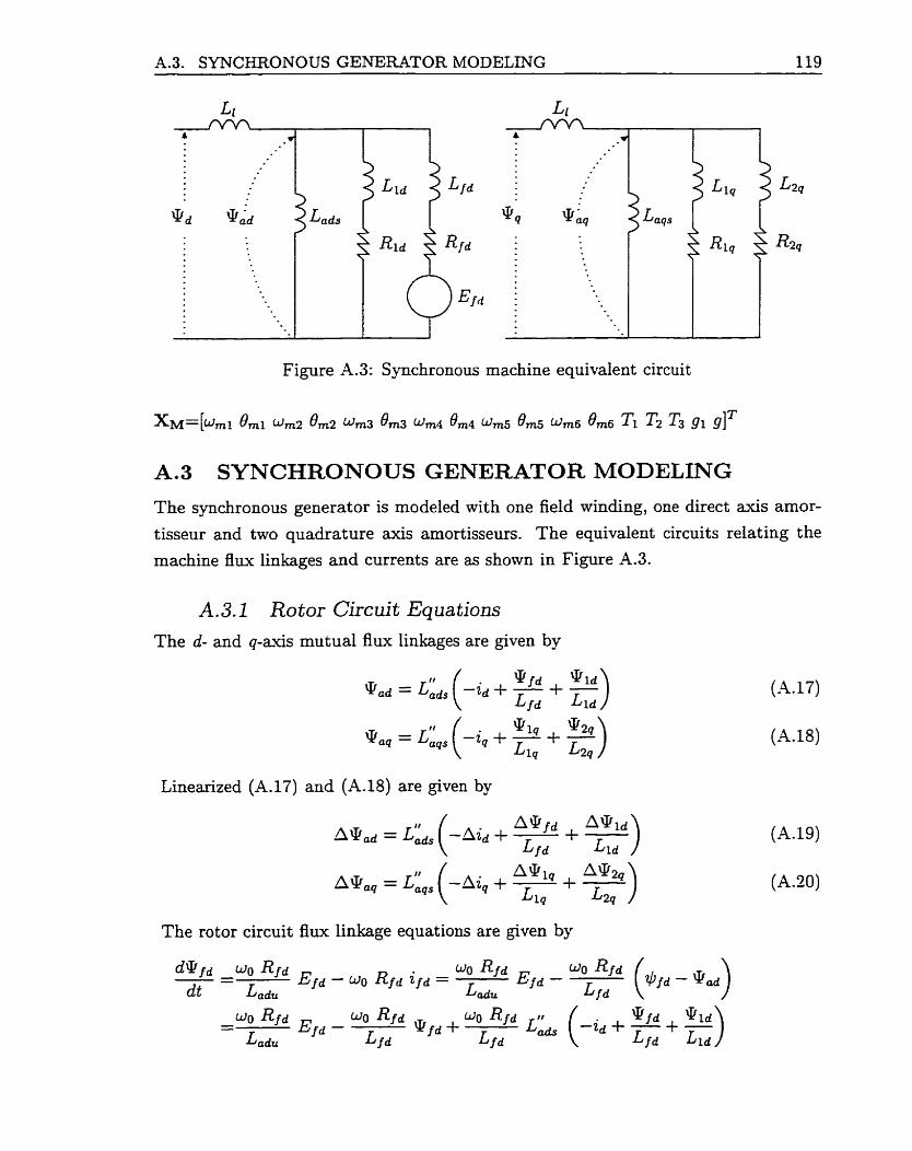
A.3. SYNCHRONOUS GENERATOR MODELING 119
Figure A.3: Synchronous machine equivalent circuit
A.3 SYNCHRONOUS GENERATOR MODELING
The synchronous generator is modeled with one field winding, one direct axis amor-
tisseur and two quadrature axis amortisseurs. The equivalent circuits relat ing the
machine flux linkages and currents are as shown in Figure A.3.
A.3.1 Rotor Circuit Equations The d- and q-axis mutual flux linkages are given by
Linearized (A.17) and (A.18) are given by
The rotor circuit flux linkage equations are given by

A.3. SYNCHRONOUS GENERATOR MODELING 120
Linearized (A.21), ( L E ) , (A.23) and (A.24) are given
(A. 24)
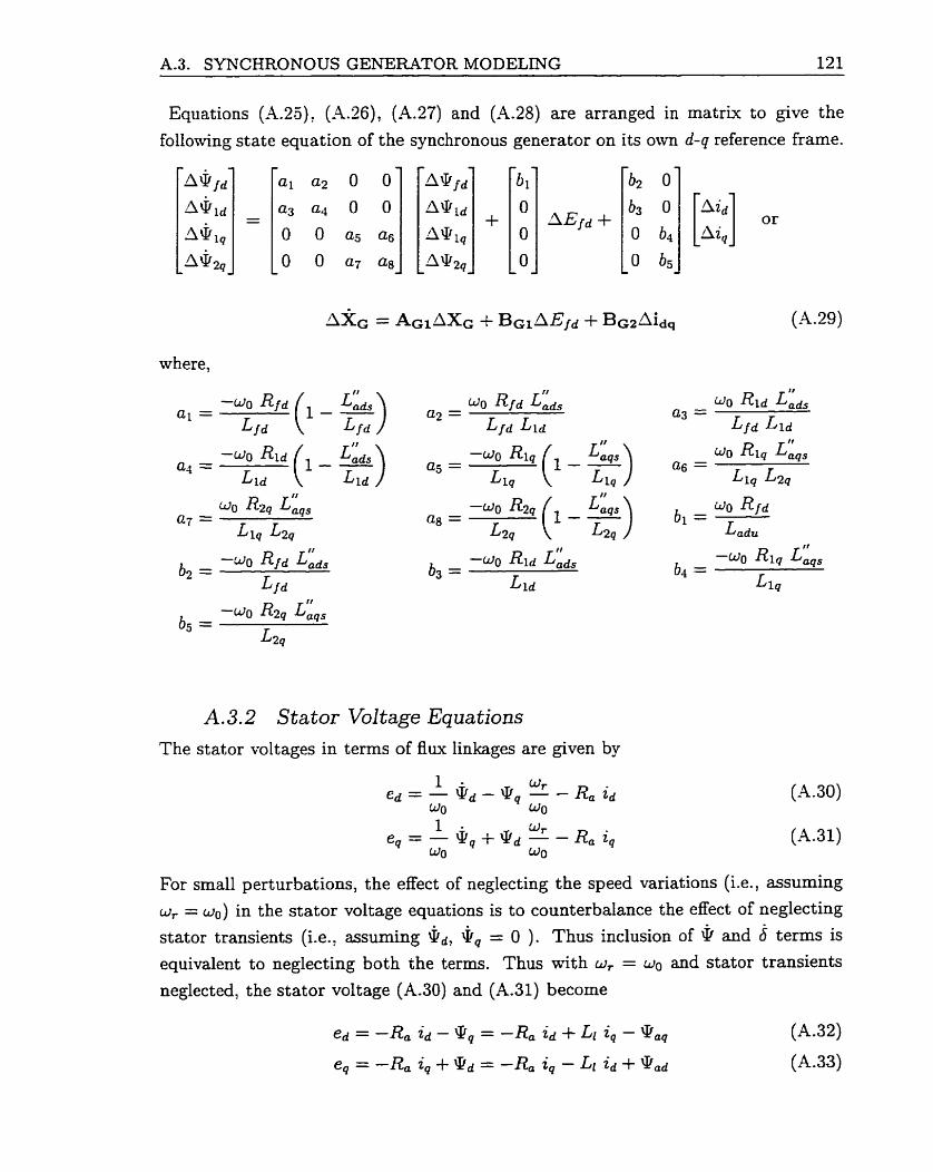
A.3. SYNCHRONOUS GENERATOR MODELING 121
Equations (A.25), (A.26), (A.27) and (-4.28) are arranged in matrùr to give the
following state equation of the synchronous generator on its own d-q reference frame.
A.3.2 Stator Voltage Equations The stator voltages in terms of flux linkages are given by
For small perturbations, the effect of neglecting the speed variations (Le., assurning
w, = wo) in the stator voltage equations is to counterbalance the effect of neglecting
stator transients (Le., assurning !bd, !bq = O ). Thuç inclusion of @ and nd terms is
equivalent to neglecting both the terms. Thus with w, = wo and stator transients
neglected, the stator voltage (A.30) and (A.31) become
A.3. SYNCHRONOUS GENERATOR MODELING 122
Substituting for iiad and Qu, from (-4.17) and (4.18), (-4.32) and (A.33) become
Linearized (A.34) and (-4.35) are given by
Thus (A.36) and (A.37) are arranged in a matrix to give the following stator voltage
equation of the synchronous generator on its own d-q reference frame.
where,
O O cl c:! [i:] = [ ~ 3 Q O 01
-~ :qr Cl =-
- G q s C2 =-
LI, L29
From (A.38) the generator stator current output equation is then derived as
A Q l d
4Qlq
A. 3.3 Electric Torque The air gap torque is given by
dl d2
+ [di di] [:::] Or
Linearized (A.40) is given by
A.3. SYNCHRONOUS GENERATOR MODELING 123
Substituting for AQad and AQ,, from (A.19) and (-4.20) respectively in (.4.41),
A.3.4 Generator Equations on Common R-1 Frame The synchronous generator self d-q axis state equation (A.29), the stator voltage
equation (-4.38) and electric torque equation (A.42) are transformed on cornmon
reference R-I axis using transformation equations described in Section -4.1-
Output Equation
Substituting value of hed, Ae, from (A.4) and Aid, Ai, from (A.5) in (A.39)
Equation (-4.43) forms the final synchronous generator output equation.
State Equation Substituting value of Aid, Ai, from (A.5) in (-4.29)
The final state equation of synchronous generator is obtained by substituting value
of AIR, AIl from (A.43) in (A.44).
A.4. EXCITATION SYSTEM MODELING 124
Figure A.4: Syncbronous generator excitation systern
Electric Torque Equation
Substituting value of hid, hi, from (A.5) in (A.42)
The final electric torque equation of synchronous generator is obtained by substitut-
ing value of AIR, AII from (A.43) in (A.46).
A.4 EXCITATION SYSTEM MODELING
Linearized (-4.48) is given by,
Substituting value of AEt from (A.7) and = 0, (A.49) becomes
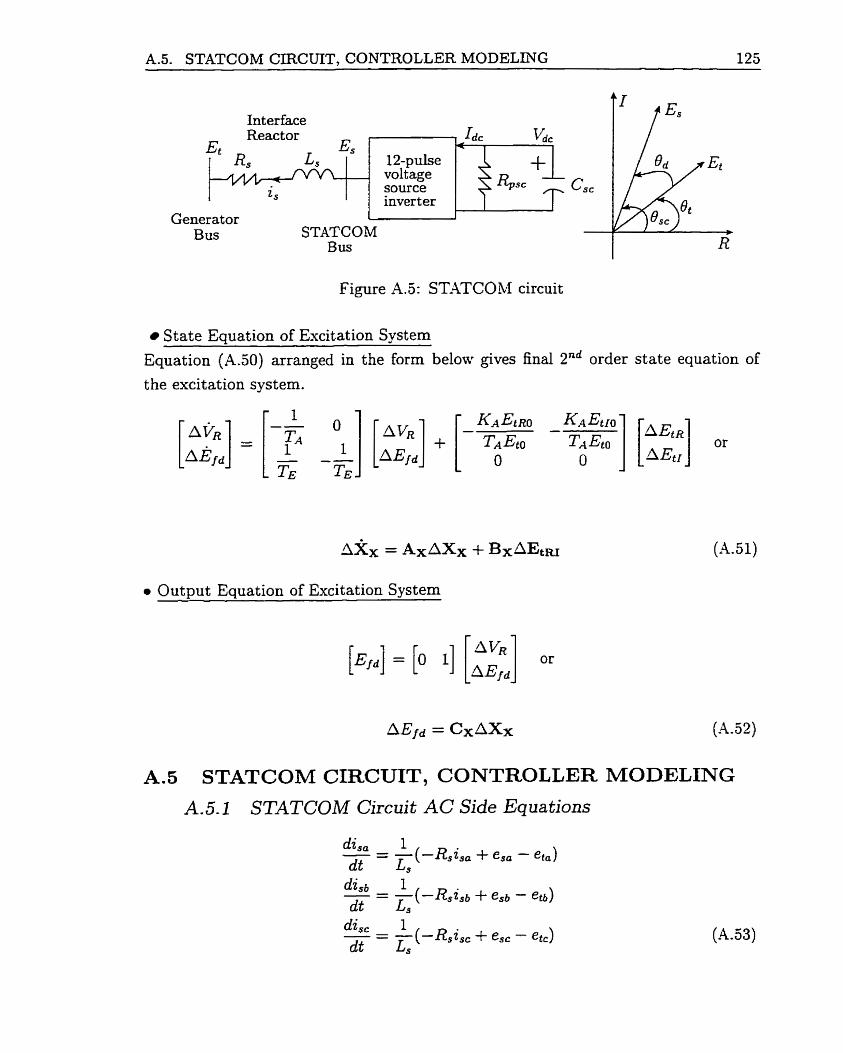
A.5. STATCOM CIRCUIT, CONTROLLER MODELmG 125
Interface -
Generator Bus
- Iàc Vdc
- STATCOM
12-pulse voltage + source %SC
invert er
Bus
5:
Figure -4.5: ST-SCOM circuit
State Equation of Excitation System
Equation (A.50) arranged in the form below gives final 2nd order state equation of
the excitation system.
Output Equation of Excitation System
A.5 STATCOM CIRCUIT, CONTROLLER MODELING
A.5.1 STATCOM Circuit AC Side Equations
di,, 1 -- - -(-Kiia + es= - e t o ) dt L,
di,, 1 -- - - ( - R S G C + est2 - etcl dt L,
A.5. STATCOM CIRCUIT, CONTROLLER MODELING 126
In matrix form (-4.53) is written as
O esa - eta [/::] =$ [r -: U ] [::il +; [esi-eti] or dt
zsc -Rs zsc esc - etc
where [Il is 3rd order identity matrix.
Converting (-4.54) on R-I frame of reference using (.4.9)
But
Therefore (A.55) becomes
Rs 0 [CR] = [z dt I S I - Wo
A.5.2 STATCOM Circuit DC Side Equations
The instantaneous power at the ac- and dc- terrninals of the inverter is equal, giving
following power balance equation
A-5. STATCOM CIRCUIT, CONTROLLER MODELING 127
where the constant 312 is chosen to match the classical phasor definition given in
Section A S . Also based on phaso: diagram sbown in Fig. -4.5: ESR and Esr can be defined as belon;
Esii =Es cos Bsc = KcscI/dc COS Ose Esr =Es sin O,, = IC,,,Vd, sin Os,
where Ka, is the constant relating ac- and dc- voltages in a 12-pulse voltage source
inverter and is given by 2&/7r. Therefore (A.59) becomes
KwcIGc COS OS, IsR + KucVdc sin Osc.ls~
Kcsc cos BscIs~ + Kcsc sin OscIs~
Substituting value of Idc in (A.58)
--- 3 - -' ( ? K - ~ cos OSCISR + -Kcsc sin OSCISI +
dt Csc 2 2
-41~0 substituting values of EsR and Esr in (A.57)
Equations (A.62) and (A.61) are arranged to get following state equation of the
STATCOM circuit.
Rs -- Kac sin O,, r r
Linearized (A.63) is given by

A.5. STATCOM CIRCUIT, CONTROLLER MODELING 128
Figure A.6: STATCOM controller
where from Fig. A.5, 8,, = Bd + Bt and ABsc = ABd.
A. 5.3 STATCOM Controller Equations
(A. 64)
Linearized (A.65) is given as below
A.5. STATCOM CIRCUIT, CONTROLLER MODELITTG 129
Kpsc ~ 8 , = (- - ~ i s c ) AXsl + (-- + K ~ ~ ~ ) AXs2 - K p ~ ~ Et RO 4Et Tmscl Tmsc2 Tmsci Er0
1 m s c ~ f i t o 1 msci 1 msc2
Equations (-4.64) and (-4.66) are cornbined to get the following equation.
where,
Kcsc sin es& a23 =
L s
~ m s c l GO O
- Kpsc E t 10
Tmscl Eto.
a32 = -3K- (sin es& I,RO - COS B , ~ I ~ ~ ~ 2 G c
3 Ka, sin Os& a36 =
2 c s c
1 mscl
1 mscl

A.6. TRANSMISSION NETWORK MODELING 130
Et EB
Figure -4.7: Transmission network
Equation (A.67) can be written as
This is the final state equation of STATCOM circuit and controller considered. The
output equation of the STATCOM is given by
A.6 TRANSMISSION NETWORK MODELING
abc abc abc abc
Converting (A.71) and (A.72) on R-I frame of reference using (A.9)
Using (A.56), (A.73) becomes
(A. 74)
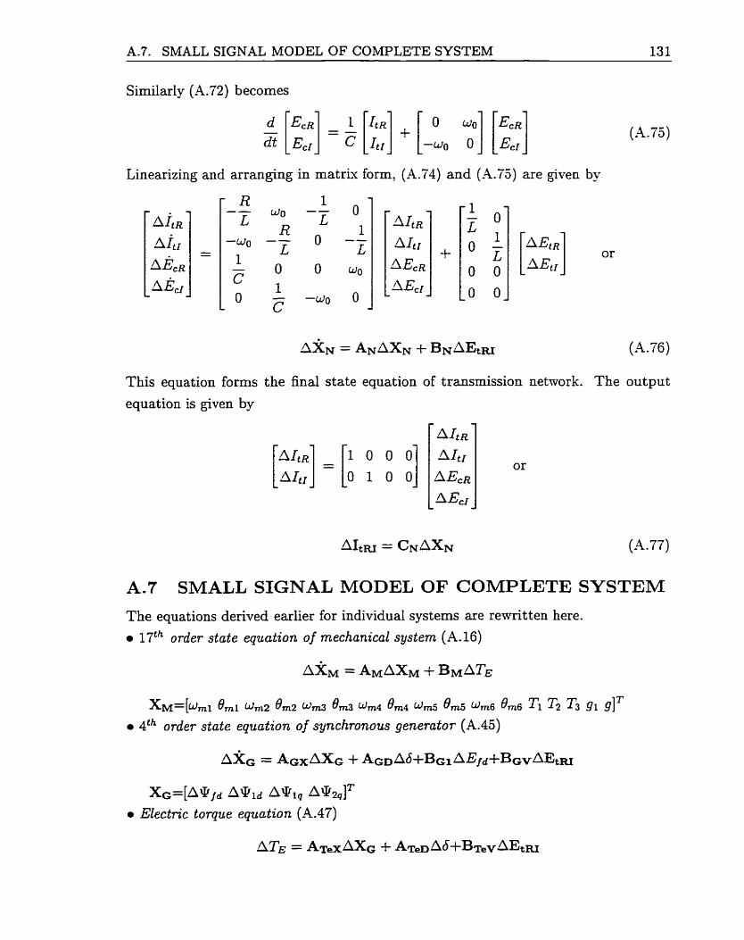
A-?. SMALL SIGNAL MODEL OF COMPLETE SYSTEM 131 --
Similarly (-4.72) becomes
Linearizing and arranging in matriu form, (A.74) and (A.75) are given by
(A. 75)
This equation forms the final state equation of transmission network. The output
equation is given by
AItRI = CNAXN (A. 77)
A.7 SMALL SIGNAL MODEL OF COMPLETE SYSTEM
The equations derived earlier for individual systems are rewritten here.
1'7 '~ order state equation of mechanical system (A.16)
Xiur=[wmi 0mi Wm2 0m2 W m 3 0m3 um4 am4 w m 5 9m5 W m 6 am6 Tl T2 T3 gl glT 0 4th order state equation of synchronous generator (A.45)
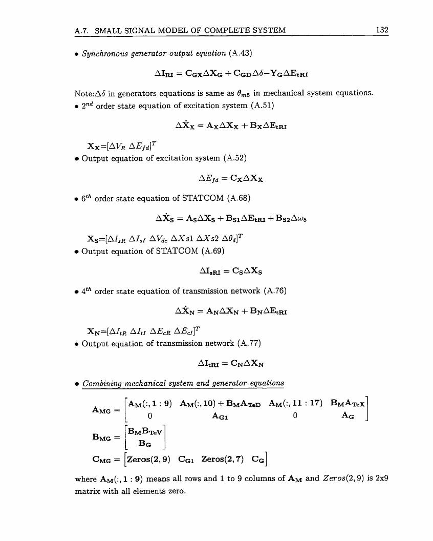
A.7. SMALL SIGNAL MODEL OF COMPLETE SYSTEM 132
0 Synchronous genemtor output equation (-4.43)
Note:Ab in generators equations is same as 0m5 in mechanical system equations.
0 2nd order state equation of excitation system (-4.51)
x x = [ A h A E ~ ~ ] * Output equation of excitation system (X.52)
LIEfd = CxAXx
0 6"" order state equation of STATCOM (-4.68)
Xs=[AIsR AIsf AVdc AXsl A X s 2 LLOdIT Output equation of ST.4TCOM (A.69)
4'h order state equation of transmission network (A.76)
X N = [ A ~ ~ R AItf AECR AEcllT 0 Output equation of transmission network (-4.77)
Combining mechanical system and generator equations
where AM(:, 1 : 9) means al1 rows and 1 to 9 columns of AM and Zeros(2,g) is 2x9
matrix with all elements zero.

A.7. SMALL SIGNAL MODEL OF COMPLETE SYSTEM 133
Cornbininq mechanical s ~ s t e m , e n e r a t o r and exciter equations
Combinin-q mechanical sgstem, -qenerator, exciter and STATCOM equations
0 Combining mechanical sgstern, .qenerator, exciter, STATCOM and network
Entire system state equation
First using generator and network output equations ILRI are eliminated
and then the 33rd order state equation of the complete system is given by

A.7. SMALL SIGNAL MODEL OF COMPLETE SYSTEM 134
Mass HP
IP
LPA
LPB
GEN
EXC
SYSTEM PARAMETERS
Base MVA = 892.4, Base kV = 500
Rotor Spring Mass System
S haft
HP-IP
IP-LPA
LPA-LPB
LPB-GEN
GEN-EXC
Iner t ia H (seconds)
0.092897
0.155589
0.85867
0.884215
0.868495
0.0342165
Spring Constant K (pu Torque/rad)
Synchronous Generator
Turbine and Governor FHP = 0.3 TCH =0.3 s KG = 25
Fyp = 0.26 TM =7.0 s TsR = 0.2 s
FLPA =0.22 Tco =0.2 s Tsbf =0.3 s FLpB d l . 2 2
0 Exciter and Voltage Regulator
KA =200 EFD maz = 7.3 TA = 0.02 s EFD min =-7-3 TE = 0.002 s
STATCOM Circuit and Controller Rs=O.O1 PU Xs=0.15 PU R, =128 PU
Cs=0.013 PU T,=0.0024 s KD=O.Ol

A-7. SMALL SIGNAL MODEL OF COMPLETE SYSTEM 135
0 Initial Operating Conditions
Generator real power =0.9 pu
Generator terminal voltage,Et=l pu
Infinite bus voltage =l pu
ST.2TCOM bus voltageoEs =0.95 pu
Definition of Percent Compensation V
where, 0.14 is the sending end transformer reactance, 0.5 is the transmission line
reactance, and 0.06 is the equivaient system reactance at infinite bus.

Appendix B
GATE PULSE GENERATION
B.1 GATE PULSES
The gate pulses for al1 the 12 switches in one phase are derived from Fig. 3.6 and
are shown in Table B.1. From this table reduced gate pulse algorithm illustrated in
Table 3.3 is derived.
Table B.1: Gate pulses output from switch firing logic
Gate Pulses
I continued on next pagc
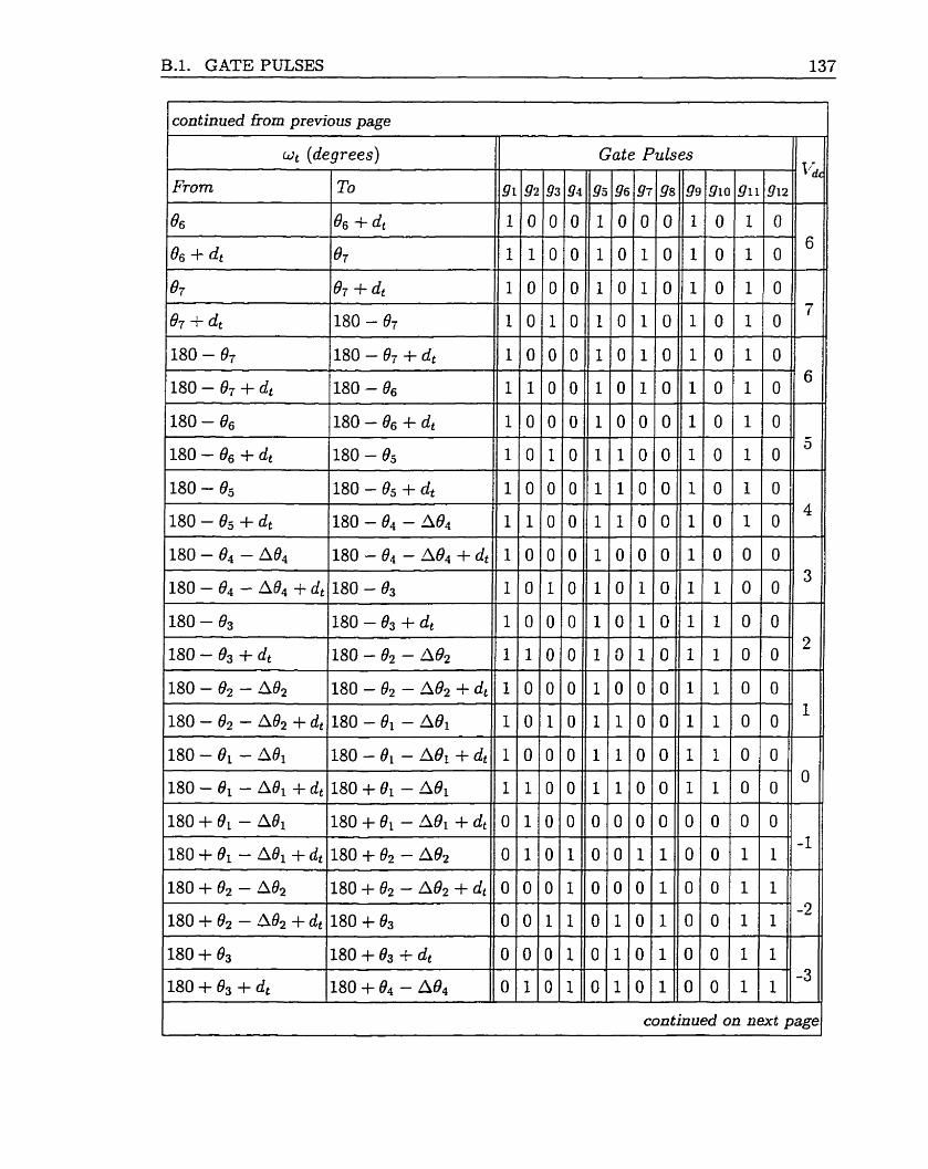
B.1. GATE PULSES 137
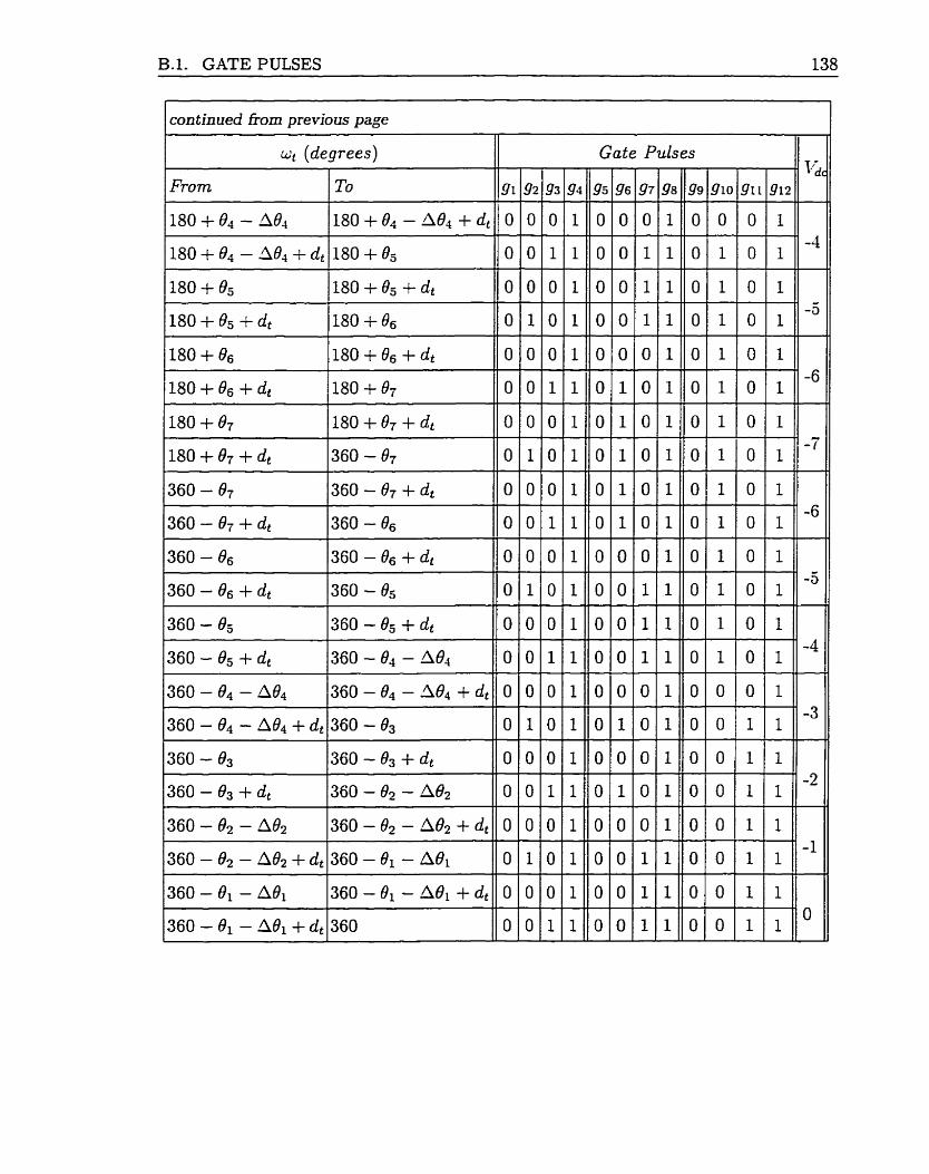
B.1. GATE PULSES 138
continued fiom previous page I I
I wt (degrees) II Gate Pulses


![[TUTORIAL] Como Reparar o Windows XP - Forum Do BABOO](https://img.dokumen.tips/doc/110x75/553c29a2550346a43f8b48a5/tutorial-como-reparar-o-windows-xp-forum-do-baboo.jpg)