Embed Size (px)
Citation preview
Zakład Energoelektroniki TWERDTWERD Power Electronics
TWERD
®
Frequency converter type:
MFC 810
3 x 1140 V2 x 250 kW
- Vector controled- Three level topology- Liquid cooled heatsink
User Manual
Part I: HardwareInstalation and technical data
www.twerd.pl

Zakład Energoelektroniki TWERD Michał Twerdul. Aleksandrowska 28-30
87-100 Toruń, Poland
tel. +48 56 654-60-91e-mail: [email protected]

Table of Contents
H.1. Safety principles..........................................................................................................................................4
H.1.1. Principles of electromagnetic compatibility (EMC)..............................................................................4
H.2. TECHNICAL DATA.....................................................................................................................................5
H.3. FREQUENCY CONVERTER INSTALLATION...........................................................................................8
H.3.1. Electrical connections..........................................................................................................................8
H.3.2. Fiber-optic connections........................................................................................................................9
H.3.2. Liquid cooling.....................................................................................................................................10
H.3.3. The printed circuit board (PCB) 810/05.............................................................................................10
H.3.4. Connection of the control circuits......................................................................................................12
H.3.5. Expansion cards................................................................................................................................13
H.3.6. Single module working mode.............................................................................................................14
Chapter: H.1. Safety principles
H.1. Safety principles
Leveling connections
Touch protection encompasses the automatic switching off of the power supply by means of the special shortcircuit (differential type) or limitation of voltages which may be touched if the insulation is damaged to a levelnot exceeding the permissible values.
Due to the intermediate circuit operation, a short to ground in the output circuit of the frequency convertermay not be detected by the short circuit protection. The frequency converter provides protection against shortcircuits between the phases and the output, but this protection is based on putting the IGBT transistors in theblocking state, which does not meet the requirements of fire protection.
In this regard, in order to ensure the staff safety, it is necessary to make local leveling connections in acorresponding way.
The special, respectively designated and protected from corrosion points for connection of the leveling wiresare provided in the frequency converter.
Protections
The are some protections provided in the frequency converter: against the motor overload, against the motoroverheat, against too low or too high voltage in the intermediate circuit of the converter, against the shortcircuit at the output of the frequency converter (protecting only the converter!!).
The switching devices
To comply with the EU Directive, in accordance with PN-EN 60204-1: 2010, a device for switching off thepower must be provided in the motor controller system, which consists of a frequency converter and anelectric machine. This device must be one of the following:
• a disconnector (with or without fuses), an AC-23B category of use that meets the requirements EN60947-3,
• a disconnector (with or without fuses), which ensures disconnection of the load circuit byopening the main contacts, complying with the requirements of EN 60947-3,
• circuit breaker complying with EN 60947-2.
Fulfilment of the requirements is the responsibility of the organization performing the installation.
Emergency stop
To comply with the EU Directive, in accordance with PN-EN 60204-1: 2010, on the basis of the staff andequipment safety, it is necessary to use an emergency stop switch, which has an advantage over otherfunctions, regardless of the operation mode. The STOP key on the operator panel cannot be considered asan emergency stop switch, because pressing it does not turn off the frequency converter from the powersupply.
Fulfilment of the requirements is the responsibility of the organization performing the installation.
Housing
The housing meets the requirements of IP00 degree of protection. The surface on which the operator panelof the frequency converter is located meets the requirements of IP00 degree of protection. The housing isdesigned in such a way that it cannot be removed without the use of tools.
Discharging capacitors
There is a battery of relatively large capacitors in the intermediate circuit of the frequency converter. After turning off the supply voltage of the frequency converter, dangerous voltage is held at its terminals for a certain time. It is necessary to wait 15 min. before switching at the terminals of the power terminal connections of the frequency converter. Information about the danger of such a voltage is on the panel, whichcloses the terminal connections of the supply voltage.
H.1.1. Principles of electromagnetic compatibility (EMC)
According to PN-EN 61800-3 (2008), part 3: “EMC requirements and special test methods”, devices forwhich:
• voltage above 1000V and • current above 400A,
belong to the C4 class. According to the requirements of the above norm, a user and a manufacturer agreeon an EMC plan to fulfil the EMC requirements for the intended use. A user determines the characteristics ofthe EMC environment taking into account the entire installation and its environment.
4 MFC810 1140V 2x 250 kW, TWERD Power Electronics

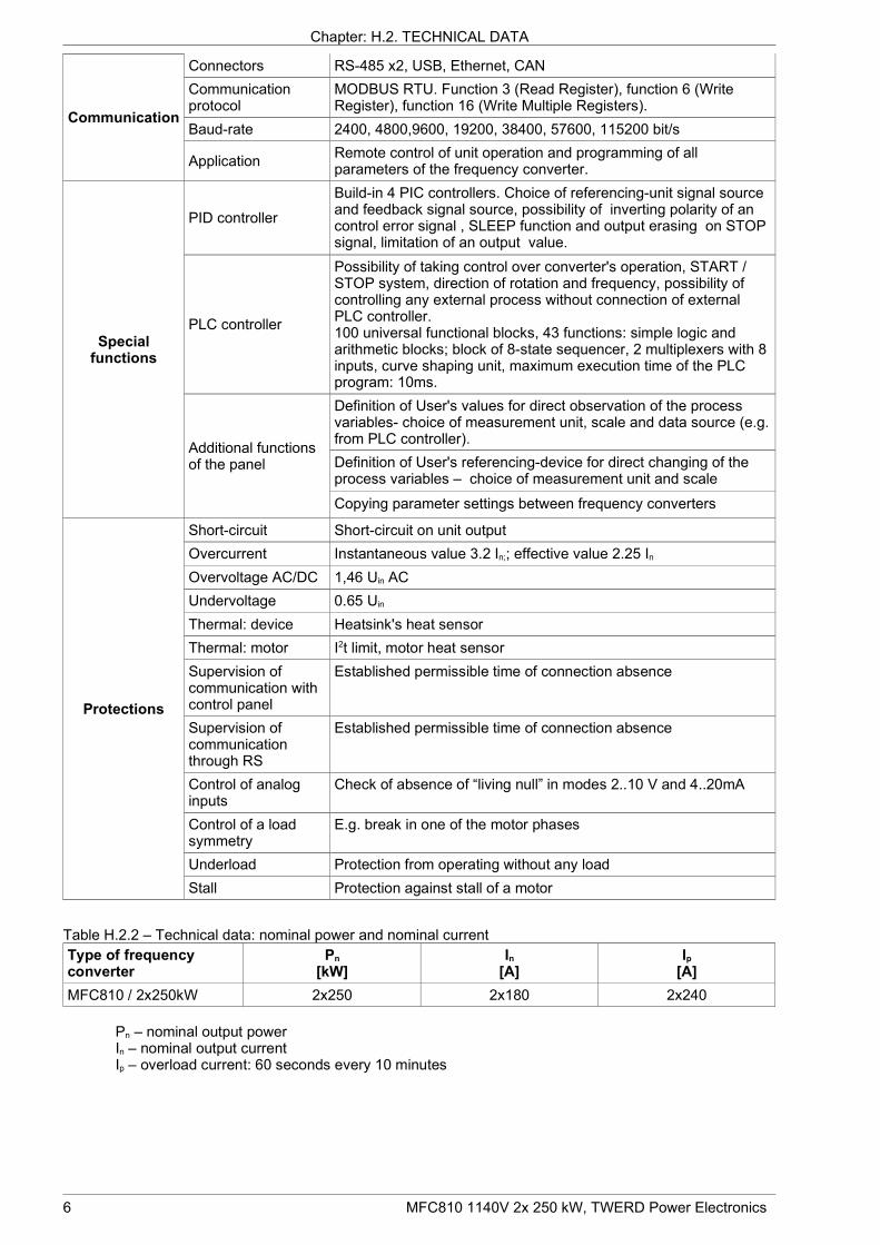
Chapter: H.2. TECHNICAL DATA
H.2. TECHNICAL DATA
Table H.2.1 shows the technical data.
Table H.2.1 – Technical data
Power supply Voltage Uin / freq. Three-phase power: 1100..1140 V (-15%, +5%), 45..66Hz
Output
Output voltage 0..Uіn [V]
Frequency0,0..400 Hz - U/f operation mode0,0..100 Hz – Vector operation mode
Frequency resolution
0.01Hz
Cooling system
Coolant Water / glycol
Inlet fluid temperature
20 – 50 0C
Coolant flow 20 l / min
Operating pressure 2.5 bar
Maximum pressure 5 bar
Internal diameter of the water/glycol supply wires
19 mm
Control system
Modulator SVPWM
Operation modeU/f (linear, exponential),Vector DTC-SVM without sensorVector DTC-SVM with sensor of the rotor position
Switching frequency 2..5 kHz (2,5 kHz for nominal power)
Rotation speed setting
Analog inputs, control panel, motopotentiometer, PID controller, communication unit RS-485 and other possibilities. Resolution of 0.1% for analog inputs or 0.1Hz / 1 rpm for the control panel and RS.
Controlinputs/outputs
Analog inputs
5 analog inputs (1 voltage mode, 4 voltage-current mode):AI0: voltage mode 0(2) ... 10V, Rin ≥ 200kΩ;AI1, AI2, AI3, AI4: voltage mode 0(2) ... 10V, Rin ≥ 100kΩ; current mode 0(4)...20mA, Rin = 250Ω,Operation mode and polarity are chosen by parameters. Accuracy:0.5 % of the full range.
Digital inputs10 digital separated inputs 0/(15...24)V, Rin ≥ 3kΩ.The possibility of obtaining up to 30 digital inputs on expansion cards.
Analog outputs
2 analog outputs (voltage-current mode)AO1, AO2: Voltage mode 0(2)...10 V Current mode 0(4)...20 mAConfigured by parameters, accuracy: 0.5%.The possibility of obtaining up to 10 digital inputs on expansion cards (2 inputs on one each expansion card).
Digital outputs
6 output relays K1 T K6 – breaking capacity: 250V/1A AC, 24V/1ADC.Fully programmable signal source. The possibility of obtaining up to 5 digital inputs on expansion cards.
Encoder interfacePossibility of direct connection of incremental encoder (A B Z optical connectors on the MFC810 / 05 board). Recommended pulse rate: 1024-2048.
Temperature sensor Pt100
MFC810 1140V 2x 250 kW, TWERD Power Electronics 5
Chapter: H.2. TECHNICAL DATA
Communication
Connectors RS-485 x2, USB, Ethernet, CAN
Communication protocol
MODBUS RTU. Function 3 (Read Register), function 6 (Write Register), function 16 (Write Multiple Registers).
Baud-rate 2400, 4800,9600, 19200, 38400, 57600, 115200 bit/s
ApplicationRemote control of unit operation and programming of all parameters of the frequency converter.
Specialfunctions
PID controller
Build-in 4 PIC controllers. Choice of referencing-unit signal source and feedback signal source, possibility of inverting polarity of an control error signal , SLEEP function and output erasing on STOP signal, limitation of an output value.
PLC controller
Possibility of taking control over converter's operation, START / STOP system, direction of rotation and frequency, possibility of controlling any external process without connection of external PLC controller.100 universal functional blocks, 43 functions: simple logic and arithmetic blocks; block of 8-state sequencer, 2 multiplexers with 8 inputs, curve shaping unit, maximum execution time of the PLC program: 10ms.
Additional functions of the panel
Definition of User's values for direct observation of the process variables- choice of measurement unit, scale and data source (e.g.from PLC controller).
Definition of User's referencing-device for direct changing of the process variables – choice of measurement unit and scale
Copying parameter settings between frequency converters
Protections
Short-circuit Short-circuit on unit output
Overcurrent Instantaneous value 3.2 In;; effective value 2.25 In
Overvoltage AC/DC 1,46 Uin AC
Undervoltage 0.65 Uin
Thermal: device Heatsink's heat sensor
Thermal: motor I2t limit, motor heat sensor
Supervision of communication with control panel
Established permissible time of connection absence
Supervision of communication through RS
Established permissible time of connection absence
Control of analog inputs
Check of absence of “living null” in modes 2..10 V and 4..20mA
Control of a load symmetry
E.g. break in one of the motor phases
Underload Protection from operating without any load
Stall Protection against stall of a motor
Table H.2.2 – Technical data: nominal power and nominal current
Type of frequency converter
Pn
[kW]In[A]
Ip[A]
MFC810 / 2x250kW 2x250 2x180 2x240
Pn – nominal output powerIn – nominal output currentIp – overload current: 60 seconds every 10 minutes
6 MFC810 1140V 2x 250 kW, TWERD Power Electronics
Chapter: H.2. TECHNICAL DATA
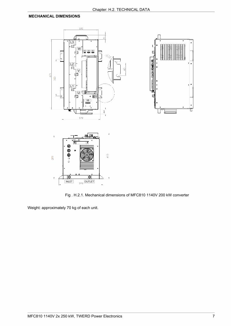
MECHANICAL DIMENSIONS
L3
L2
L1
U
V
W
X8
X2X4X3
X0
INLET OUTLET
Fig . H.2.1. Mechanical dimensions of MFC810 1140V 200 kW converter
Weight: approximately 70 kg of each unit.
MFC810 1140V 2x 250 kW, TWERD Power Electronics 7
Chapter: H.3. FREQUENCY CONVERTER INSTALLATION
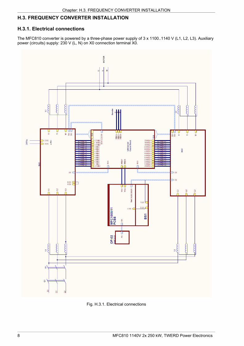
H.3. FREQUENCY CONVERTER INSTALLATION
H.3.1. Electrical connections
The MFC810 converter is powered by a three-phase power supply of 3 x 1100..1140 V (L1, L2, L3). Auxiliary power (circuits) supply: 230 V (L, N) on X0 connection terminal X0.
Fig. H.3.1. Electrical connections
8 MFC810 1140V 2x 250 kW, TWERD Power Electronics
Chapter: H.3. FREQUENCY CONVERTER INSTALLATION
L3
L2
L1
U
V
W
X8
X2X4X3
X0
L3
L2
L1
U
V
W
X8
X2X4X3
X0
X1
8
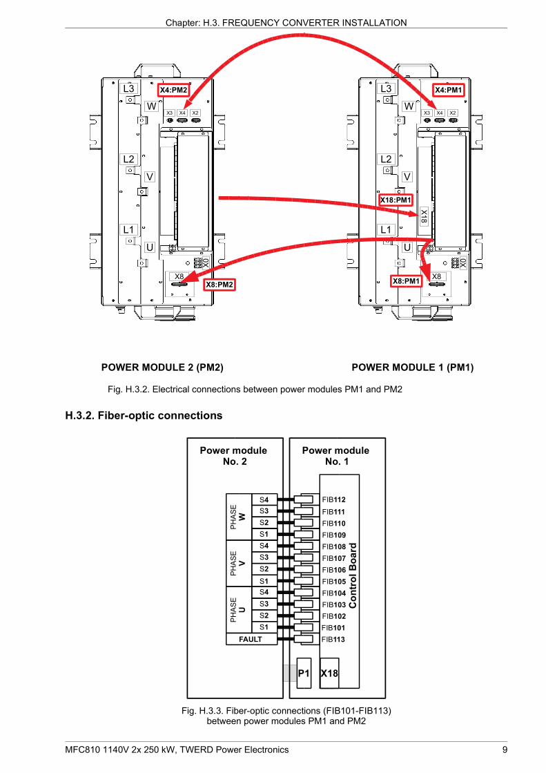
POWER MODULE 2 (PM2) POWER MODULE 1 (PM1)
X4:PM2 X4:PM1
X8:PM1
X18:PM1
X8:PM2
Fig. H.3.2. Electrical connections between power modules PM1 and PM2
H.3.2. Fiber-optic connections
FAULT
S1
S2
S3
S4
PH
AS
E
U
S1
S2
S3
S4
PH
AS
E
V
S1
S2
S3
S4
PH
AS
E
W
Power module No. 2
Control Board
FIB113
FIB101
FIB102
FIB103
FIB104
FIB105
FIB106
FIB107
FIB108
FIB109
FIB110
FIB111
FIB112
X18P1
Power module No. 1
Fig. H.3.3. Fiber-optic connections (FIB101-FIB113)between power modules PM1 and PM2
MFC810 1140V 2x 250 kW, TWERD Power Electronics 9
Chapter: H.3. FREQUENCY CONVERTER INSTALLATION
H.3.2. Liquid cooling
It is necessary to connect hoses and to provide a stream of cooling liquid to every power block (fig. H.2.1 - inlet/outlet), according to the data from the table H.2.1.
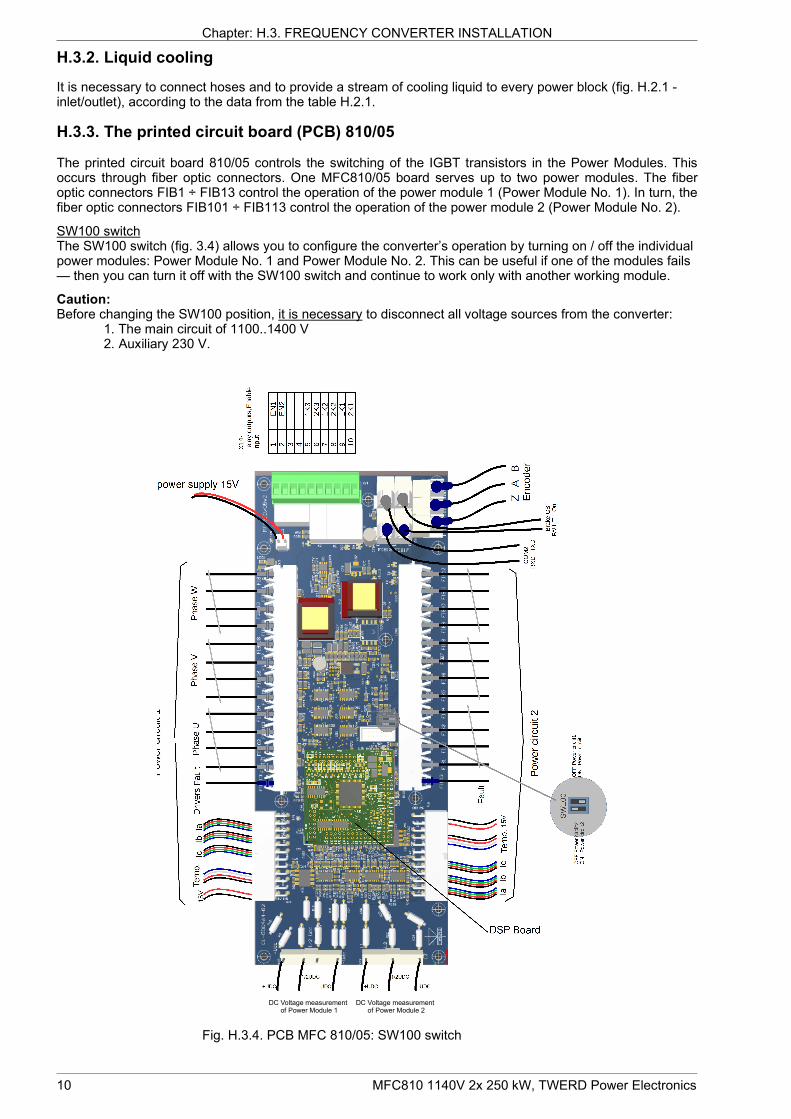
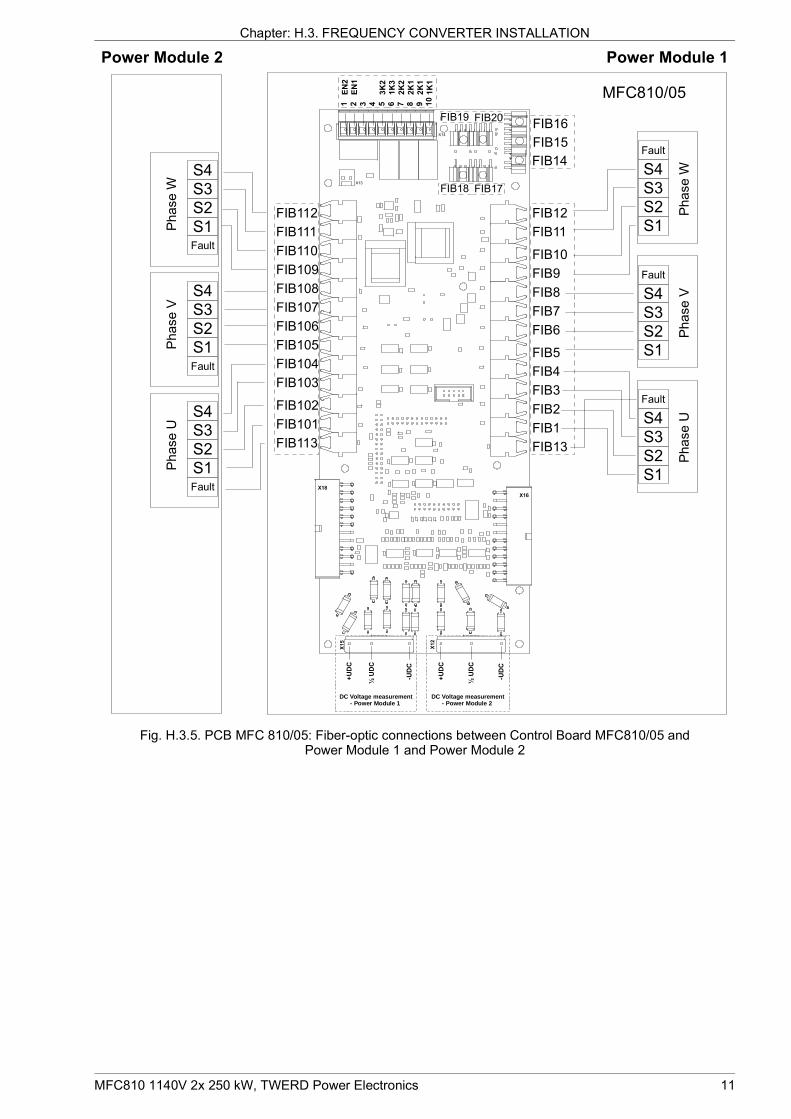
H.3.3. The printed circuit board (PCB) 810/05
The printed circuit board 810/05 controls the switching of the IGBT transistors in the Power Modules. Thisoccurs through fiber optic connectors. One MFC810/05 board serves up to two power modules. The fiberoptic connectors FIB1 ÷ FIB13 control the operation of the power module 1 (Power Module No. 1). In turn, thefiber optic connectors FIB101 ÷ FIB113 control the operation of the power module 2 (Power Module No. 2).
SW100 switchThe SW100 switch (fig. 3.4) allows you to configure the converter’s operation by turning on / off the individual power modules: Power Module No. 1 and Power Module No. 2. This can be useful if one of the modules fails — then you can turn it off with the SW100 switch and continue to work only with another working module.
Caution:Before changing the SW100 position, it is necessary to disconnect all voltage sources from the converter:
1. The main circuit of 1100..1400 V2. Auxiliary 230 V.
DC Voltage measurement of Power Module 1
DC Voltage measurement of Power Module 2
Fig. H.3.4. PCB MFC 810/05: SW100 switch
10 MFC810 1140V 2x 250 kW, TWERD Power Electronics
Chapter: H.3. FREQUENCY CONVERTER INSTALLATION
Fig. H.3.5. PCB MFC 810/05: Fiber-optic connections between Control Board MFC810/05 andPower Module 1 and Power Module 2
MFC810 1140V 2x 250 kW, TWERD Power Electronics 11
FIB12
FIB11
FIB10
FIB9
FIB8
FIB6
FIB5
FIB4
FIB3
FIB2
FIB1
FIB13
FIB7
FIB112
MFC810/05
FIB111
FIB110
FIB109
FIB108
FIB107
FIB106
FIB105
FIB104
FIB103
FIB102
FIB101
FIB113
S4
S3
S2
S1
Phase W
Fault
S4
S3
S2
S1Phase W
Fault
S4
S3
S2
S1
Phase V
Fault
S4
S3
S2
S1
Phase U
Fault
Power Module 1
S4
S3
S2S1P
hase V
Fault
S4
S3
S2
S1Phase U
Fault
X15
+UDC
½ UDC
-UDC
X12
FIB14
FIB15
FIB16
FIB18 FIB17
FIB19 FIB20
1 2 3 4 5 6 7 8 9 10
EN2
EN1
3K2
1K3
2K2
2K1
2K1
1K1
X14
X13
X18
X16
Power Module 2
+UDC
½ UDC
-UDC
DC Voltage measurement- Power Module 1
DC Voltage measurement- Power Module 2
Chapter: H.3. FREQUENCY CONVERTER INSTALLATION
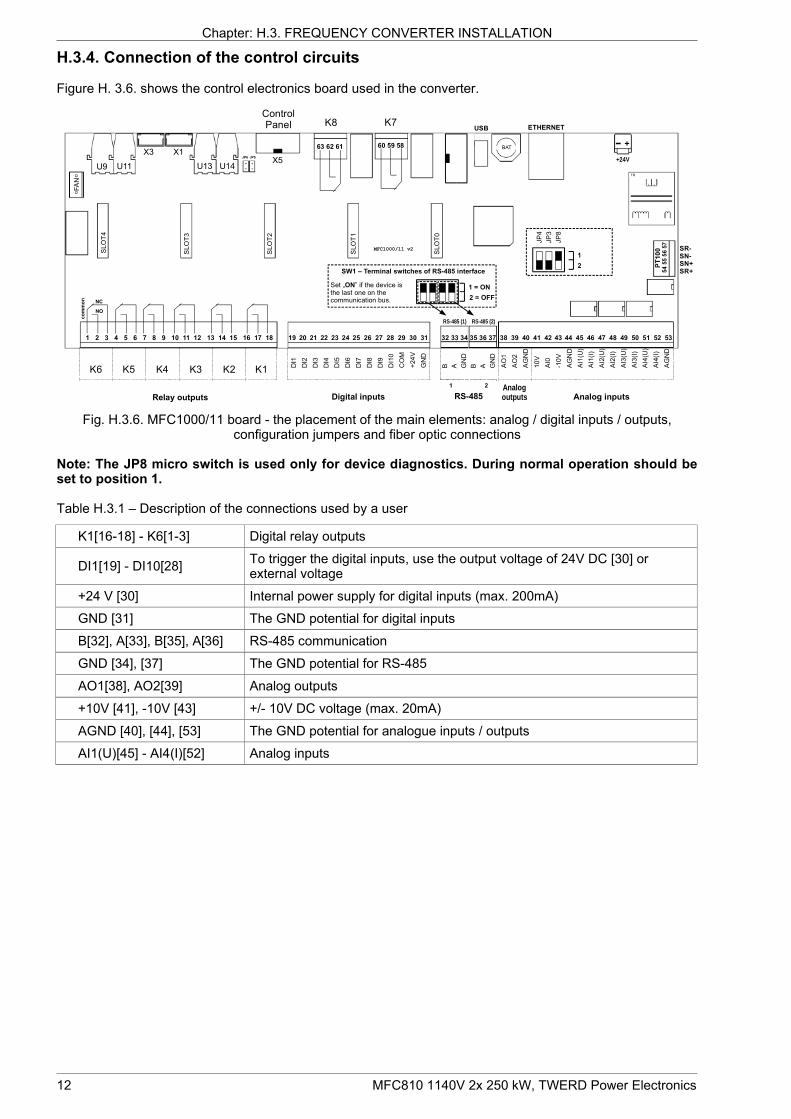
H.3.4. Connection of the control circuits
Figure H. 3.6. shows the control electronics board used in the converter.
1 2 3 4 5 6 7 8 9 10 11 12 13 14 15 16 17 18 19 20 21 22 23 24 25 26 27 28 29 30 31 32 33 34 35 36 37 38 39 40 41 42 43 44 45 46 47 48 49 50 51 52 53
DI1
DI2
DI3
DI4
DI5
DI6
DI7
DI8
DI9
DI1
0
CO
M
+24
V
GN
D
B A GN
D
B A GN
D
AO
1
AO
2
AG
ND
10
V
AI0
-10
V
AG
ND
AI1
(U)
AI1
(I)
AI2
(U)
AI2
(I)
AI3
(U)
AI3
(I)
AI4
(U)
AI4
(I)
AG
ND
SLO
T4
SLO
T3
SLO
T2
SLO
T1
FA
N
SLO
T0
54 55 56 57
SR-SN-SN+SR+
PT100
+24V
ETHERNET
BAT
USB
JTAG
K7
60 59 58 63 62 61
K8
TR
JP6 JP5
TR
common NC
NO
U9 U11 U13 U14
K1K2K3K4K5K6
ControlPanel
X3 X1X5
+
Relay outputs Digital inputs Analog inputsAnalogoutputs
2 = OFF
1 = ON
SW1 – Terminal switches of RS-485 interface
Set „ON” if the device isthe last one on thecommunication bus.
2
1
JP
4
JP
3
JP
8
MFC1000/11 v2
RS-485 (1) RS-485 (2)
RS-485
1 2
Fig. H.3.6. MFC1000/11 board - the placement of the main elements: analog / digital inputs / outputs,configuration jumpers and fiber optic connections
Note: The JP8 micro switch is used only for device diagnostics. During normal operation should beset to position 1.
Table H.3.1 – Description of the connections used by a user
K1[16-18] - K6[1-3] Digital relay outputs
DI1[19] - DI10[28]To trigger the digital inputs, use the output voltage of 24V DC [30] or external voltage
+24 V [30] Internal power supply for digital inputs (max. 200mA)
GND [31] The GND potential for digital inputs
B[32], A[33], B[35], A[36] RS-485 communication
GND [34], [37] The GND potential for RS-485
AO1[38], AO2[39] Analog outputs
+10V [41], -10V [43] +/- 10V DC voltage (max. 20mA)
AGND [40], [44], [53] The GND potential for analogue inputs / outputs
AI1(U)[45] - AI4(I)[52] Analog inputs
12 MFC810 1140V 2x 250 kW, TWERD Power Electronics

Chapter: H.3. FREQUENCY CONVERTER INSTALLATION
Digital inputs can work in two variants: common ground or common + 24V. The choice of the variant is made by shortening the clamps on the terminal block: variant 1 - common mass: COM - GND terminals variant 2 - common + 24V: COM terminals - + 24V
DI1 DI2 DI3 DI4 DI5 DI6 DI7 DI8 DI9 DI10 COM +24V GND
S1 S2 S3 S4 S5 S6 S7 S8 S9 S10
DI1 DI2 DI3 DI4 DI5 DI6 DI7 DI8 DI9 DI10 COM +24V GND
S1 S2 S3 S4 S5 S6 S7 S8 S9 S10
Variant 1
Variant 2
Fig. 3.7: Two variants of using digital inputs: variant 1 and 2. The internal connections of the boardare marked by a dashed line.S1 ÷ S10: exemplary connectors to switch on/off the digital inputs.
H.3.5. Expansion cards
Expansion cards enable extending the drive with additional inputs / outputs. There are 5 slots available: 0 ÷ 4.In each of them, one expansion card can be installed. Expansion boards are available:
- 6 digital inputs,- 6 digital outputs,- 3 relay outputs,- 2 analog outputs.
MFC810 1140V 2x 250 kW, TWERD Power Electronics 13
Chapter: H.3. FREQUENCY CONVERTER INSTALLATION
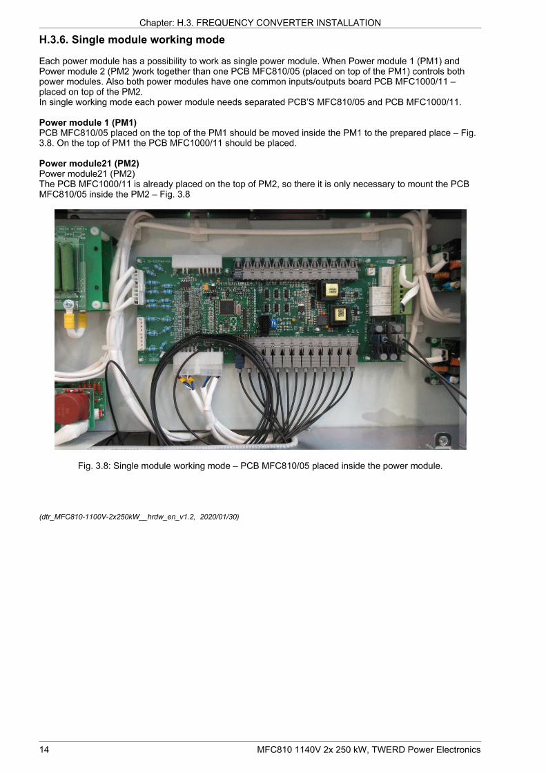
H.3.6. Single module working mode
Each power module has a possibility to work as single power module. When Power module 1 (PM1) and Power module 2 (PM2 )work together than one PCB MFC810/05 (placed on top of the PM1) controls both power modules. Also both power modules have one common inputs/outputs board PCB MFC1000/11 – placed on top of the PM2. In single working mode each power module needs separated PCB’S MFC810/05 and PCB MFC1000/11.
Power module 1 (PM1)PCB MFC810/05 placed on the top of the PM1 should be moved inside the PM1 to the prepared place – Fig.3.8. On the top of PM1 the PCB MFC1000/11 should be placed.
Power module21 (PM2)Power module21 (PM2) The PCB MFC1000/11 is already placed on the top of PM2, so there it is only necessary to mount the PCB MFC810/05 inside the PM2 – Fig. 3.8
Fig. 3.8: Single module working mode – PCB MFC810/05 placed inside the power module.
(dtr_MFC810-1100V-2x250kW__hrdw_en_v1.2, 2020/01/30)
14 MFC810 1140V 2x 250 kW, TWERD Power Electronics
MFC810, MFC1000 Appendix A: Configuration Parameters A.1/33
Appendix A: Configuration Parameters
Software version: 1.98 rev.3Document version: 1.4
Read-only parameters
Group Name The description
GROUP 00 – Electric motor
00.00 N processSpeed of process. It depends on current rotation speed of the electric motor. It is possible to set up scale, measurement unit and number of decimal places for this parameter using parameters 42.01, 42.02 and 42.03
00.01 Motor n Current rotation speed of the electric motor in rotations per one minute [rpm]
00.02 Ref. n Value of the referenced rotation speed [rpm]
00.03 f out Current output frequency of the converter [Hz]
00.04 f ref. Referenced frequency [Hz]
00.05 Mot torque The moment of the drive compared to the nominal moment [%]
00.06 Motor curr. Average value of current in windings of the motor [A]
00.07 Motor volt. An output voltage AC of the converter [V] (voltage of the motor) – interfacial voltage
00.08 Motor temp. Higher of temperatures indicated by parameters 00.28 and 00.48 [%]
00.09 Output power Current output power of the converter at [kW]
00.10 Power factor Output power factor
00.11Energy Value of energy which has been transferred to the electric motor from the time of first
switching on the converter [kWh]
00.12 Psi st. Stator stream [Wb]
00.13 Ia curr. RMS current of a phase A of the motor [A]
00.14 Ib curr. RMS current of a phase B of the motor [A]
00.15 Ic curr. RMS current of a phase C of the motor [A]
00.16 Encoder n Encoder speed [rpm]
00.28 Motor temp. 1 Calculated relative temperature of the motor 1 [%]
00.33 Ia 1 curr. RMS current of a phase A of the motor 1 [A]
00.34 Ib 1 curr. RMS current of a phase B of the motor 1 [A]
00.35 Ic 1 curr. RMS current of a phase C of the motor 1 [A]
00.48 Motor temp. 2 Calculated relative temperature of the motor 2 [%]
00.53 Ia 2 curr. RMS current of a phase A of the motor 2 [A]
00.54 Ib 2 curr. RMS current of a phase B of the motor 2 [A]
00.55 Ic 2 curr. RMS current of a phase C of the motor 2 [A]
GROUP 01 – Power circuit
01.01 DC volt. Voltage of the DC-link circuit of the converter [V]
01.02 DC volt. 1Voltage of the first half DC-link circuit of the converter [V] (only three-level inverters)
01.03 DC volt. 2Voltage of the second half DC-link circuit of the converter [V] (only three-level inverters)
01.04 DC balanceBalance between DC volt 1 and DC volt 2 [%](only three-level inverters)
01.05 Grid volt.Power line supply AC voltage [V] – estimated. The calculation is based on the DC-link voltageUdc measurement.
01.06 Grid freq. Line Voltage frequency [Hz]
01.07 Active pow Active power
01.08 Reactive pow Reactive power
01.09 L1 curr. RMS current of a phase L1 of the line [A]
01.10 L2 curr. RMS current of a phase L2 of the line [A]
01.11 L3 curr. RMS current of a phase L3 of the line [A]
GROUP 02 – Temperature
02.01 VSD temp 1 Temperature of the VSD's IGBT module 1 [°C]
02.02 VSD temp 2 Temperature of the VSD's IGBT module 2 [°C]
02.03 VSD temp 3 Temperature of the VSD's IGBT module 3 [°C]
02.04 VSD inlet Temperature of the VSD inlet (only in liquid cooled inverter) [°C]
TWERD Power Electronics – www.twerd.pl

A.2/33 Appendix A: Configuration Parameters MFC810, MFC1000
Group Name The description
02.05 VSD outlet Temperature of the VSD outlet (only in liquid cooled inverter) [°C]
02.06 VSD temp 4 Temperature of the VSD's IGBT module 4 [°C]
02.07 VSD temp 5 Temperature of the VSD's IGBT module 5 [°C]
02.08 VSD temp 6 Temperature of the VSD's IGBT module 6 [°C]
02.09 VSD temp 7 Temperature of the VSD's IGBT module 7 [°C]
02.10 VSD temp 8 Temperature of the VSD's IGBT module 8 [°C]
02.11 VSD temp 9 Temperature of the VSD's IGBT module 9 [°C]
02.12 VSD temp 10 Temperature of the VSD's IGBT module 10 [°C]
02.13 VSD temp 11 Temperature of the VSD's IGBT module 11 [°C]
02.14 VSD temp 12 Temperature of the VSD's IGBT module 12 [°C]
02.15 VSD temp max The highest temperature of “VSD temp 1” .. “VSD temp 12” [°C]
02.23 ACR temp 1 Temperature of the ACR's IGBT module 1 [°C]
02.22 ACR temp 2 Temperature of the ACR's IGBT module 2 [°C]
02.23 ACR temp 3 Temperature of the ACR's IGBT module 3 [°C]
02.24 ACR inlet Temperature of the ACR inlet (only in liquid cooled inverter) [°C]
02.25 ACR outlet Temperature of the ACR outlet (only in liquid cooled inverter) [°C]
02.26 ACR temp 4 Temperature of the ACR's IGBT module 4 [°C]
02.27 ACR temp 5 Temperature of the ACR's IGBT module 5 [°C]
02.28 ACR temp 6 Temperature of the ACR's IGBT module 6 [°C]
02.29 ACR temp 7 Temperature of the ACR's IGBT module 7 [°C]
02.30 ACR temp 8 Temperature of the ACR's IGBT module 8 [°C]
02.31 ACR temp 9 Temperature of the ACR's IGBT module 9 [°C]
02.32 ACR temp 10 Temperature of the ACR's IGBT module 10 [°C]
02.33 ACR temp 11 Temperature of the ACR's IGBT module 11 [°C]
02.34 ACR temp 12 Temperature of the ACR's IGBT module 12 [°C]
02.35 ACR temp max The highest temperature of “ACR temp 1” .. “ACR temp 12” [°C]
02.40 PT 100 Temperature of the PT100 sensor
02.41 Ctrl temp 1 Service parameter
02.42 Ctrl temp 2 Service parameter
02.43 Ctrl temp 3 Service parameter
02.44 Ctrl temp 4 Service parameter
02.45 Ctrl temp 5 Service parameter
02.46 Ctrl temp 6 Service parameter
02.47 Ctrl temp 7 Service parameter
02.48 Ctrl temp 8 Service parameter
02.49 Ctrl temp 9 Service parameter
02.50 Ctrl temp 10 Service parameter
02.51 Ctrl temp 11 Service parameter
02.52 Ctrl temp 12 Service parameter
02.53 Ctrl temp 13 Service parameter
02.54 Ctrl temp 14 Service parameter
02.55 Ctrl temp 15 Service parameter
GROUP 03 – Inputs / outputs
03.01 DI state 1 Status of digital inputs 1..10
03.02 DI state 2 Status of digital inputs 11..20
03.03 DI state 3 Status of digital inputs 21..30
03.04 DI state 4 Status of digital inputs 31..40
03.05 DI state 5 Status of digital inputs 41..50
03.06 DI state 6 Status of digital inputs 51..60
03.11 DO state 1 Status of digital outputs 1..8
03.12 DO state 2 Status of digital outputs 11..18
03.13 DO state 3 Status of digital outputs 21..28
03.14 DO state 4 Status of digital outputs 31..38
03.15 DO state 5 Status of digital outputs 41..48
03.16 DO state 6 Status of digital outputs 51..58
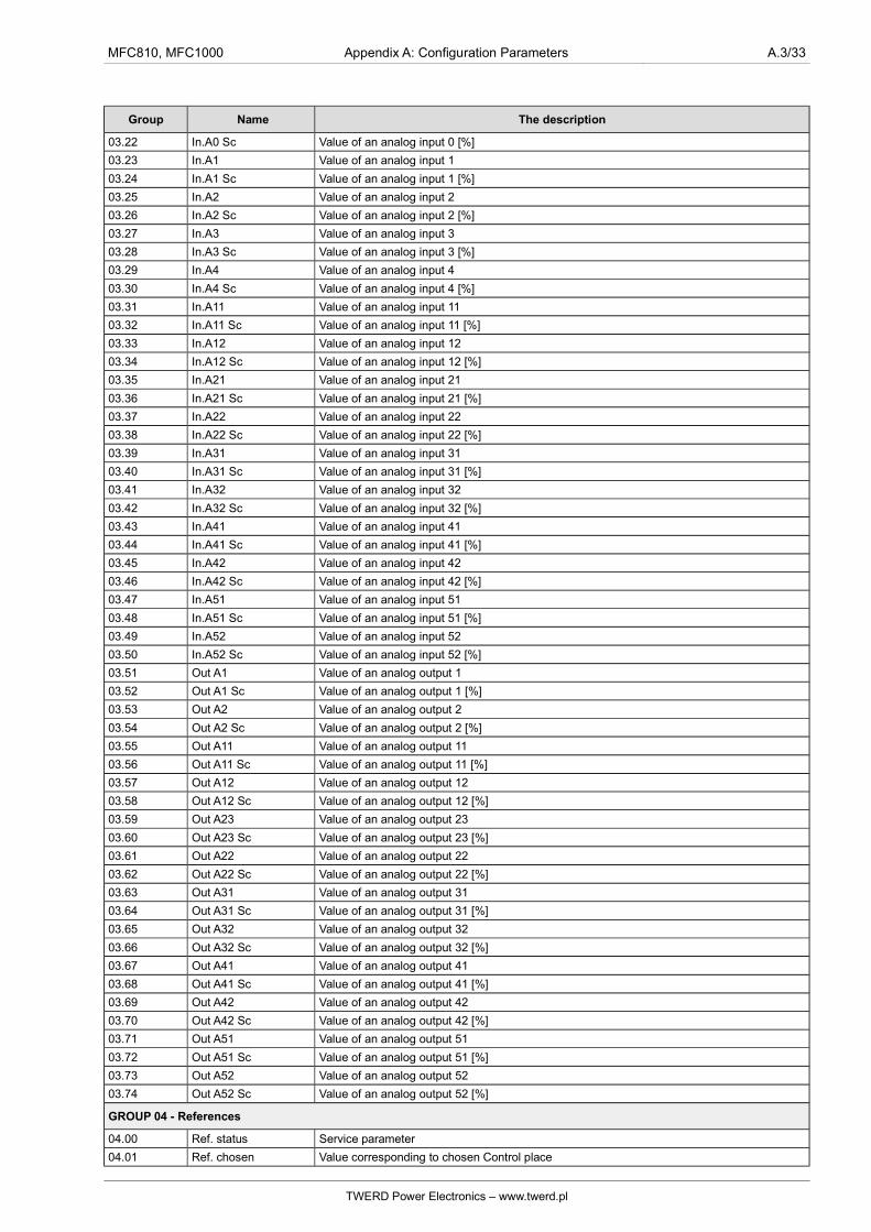
03.23 In.A0 Value of an analog input 0
TWERD Power Electronics – www.twerd.pl
MFC810, MFC1000 Appendix A: Configuration Parameters A.3/33
Group Name The description
03.22 In.A0 Sc Value of an analog input 0 [%]
03.23 In.A1 Value of an analog input 1
03.24 In.A1 Sc Value of an analog input 1 [%]
03.25 In.A2 Value of an analog input 2
03.26 In.A2 Sc Value of an analog input 2 [%]
03.27 In.A3 Value of an analog input 3
03.28 In.A3 Sc Value of an analog input 3 [%]
03.29 In.A4 Value of an analog input 4
03.30 In.A4 Sc Value of an analog input 4 [%]
03.31 In.A11 Value of an analog input 11
03.32 In.A11 Sc Value of an analog input 11 [%]
03.33 In.A12 Value of an analog input 12
03.34 In.A12 Sc Value of an analog input 12 [%]
03.35 In.A21 Value of an analog input 21
03.36 In.A21 Sc Value of an analog input 21 [%]
03.37 In.A22 Value of an analog input 22
03.38 In.A22 Sc Value of an analog input 22 [%]
03.39 In.A31 Value of an analog input 31
03.40 In.A31 Sc Value of an analog input 31 [%]
03.41 In.A32 Value of an analog input 32
03.42 In.A32 Sc Value of an analog input 32 [%]
03.43 In.A41 Value of an analog input 41
03.44 In.A41 Sc Value of an analog input 41 [%]
03.45 In.A42 Value of an analog input 42
03.46 In.A42 Sc Value of an analog input 42 [%]
03.47 In.A51 Value of an analog input 51
03.48 In.A51 Sc Value of an analog input 51 [%]
03.49 In.A52 Value of an analog input 52
03.50 In.A52 Sc Value of an analog input 52 [%]
03.51 Out A1 Value of an analog output 1
03.52 Out A1 Sc Value of an analog output 1 [%]
03.53 Out A2 Value of an analog output 2
03.54 Out A2 Sc Value of an analog output 2 [%]
03.55 Out A11 Value of an analog output 11
03.56 Out A11 Sc Value of an analog output 11 [%]
03.57 Out A12 Value of an analog output 12
03.58 Out A12 Sc Value of an analog output 12 [%]
03.59 Out A23 Value of an analog output 23
03.60 Out A23 Sc Value of an analog output 23 [%]
03.61 Out A22 Value of an analog output 22
03.62 Out A22 Sc Value of an analog output 22 [%]
03.63 Out A31 Value of an analog output 31
03.64 Out A31 Sc Value of an analog output 31 [%]
03.65 Out A32 Value of an analog output 32
03.66 Out A32 Sc Value of an analog output 32 [%]
03.67 Out A41 Value of an analog output 41
03.68 Out A41 Sc Value of an analog output 41 [%]
03.69 Out A42 Value of an analog output 42
03.70 Out A42 Sc Value of an analog output 42 [%]
03.71 Out A51 Value of an analog output 51
03.72 Out A51 Sc Value of an analog output 51 [%]
03.73 Out A52 Value of an analog output 52
03.74 Out A52 Sc Value of an analog output 52 [%]
GROUP 04 - References
04.00 Ref. status Service parameter
04.01 Ref. chosen Value corresponding to chosen Control place
TWERD Power Electronics – www.twerd.pl

A.4/33 Appendix A: Configuration Parameters MFC810, MFC1000
Group Name The description
04.02 Ref. act. A1 Ref. value of Control place A1
04.03 Ref. act. A2 Ref. value of Control place A2
04.04 Ref. act. B1 Ref. value of Control place B1
04.05 Ref. act. B2 Ref. value of Control place B2
04.11 PID 1 ref Value of current referencing-unit of the PID 1 controller [%]
04.12 PID 1 inp. Current input value of the PID 1 controller [%]
04.13 PID 1 err. Error of the PID 1 controller [%]
04.14 PID 1 out. Current output value of the PID 1 controller [%]
04.23 PID 2 ref Value of current referencing-unit of the PID 2 controller [%]
04.22 PID 2 inp. Current input value of the PID 2 controller [%]
04.23 PID 2 err. Error of the PID 2 controller [%]
04.24 PID 2 out. Current output value of the PID 2 controller [%]
04.31 PID 3 ref Value of current referencing-unit of the PID 3 controller [%]
04.32 PID 3 inp. Current input value of the PID 3 controller [%]
04.33 PID 3 err. Error of the PID 3 controller [%]
04.34 PID 3 out. Current output value of the PID 3 controller [%]
04.41 PID 4 ref Value of current referencing-unit of the PID 4 controller [%]
04.42 PID 4 inp. Current input value of the PID 4 controller [%]
04.43 PID 4 err. Error of the PID 4 controller [%]
04.44 PID 4 out. Current output value of the PID 4 controller [%]
04.51 Ref user 1 User 1 reference
04.52 Ref user 2 User 2 reference
04.53 Ref user 3 User 3 reference
04.54 Ref user 4 User 4 reference
04.55 Ref user 5 User 5 reference
04.56 Ref user 6 User 6 reference
04.57 Ref user 7 User 7 reference
04.58 Ref user 8 User 8 reference
04.59 Ref user 9 User 9 reference
04.60 Ref user 10 User 10 reference
GROUP 05 - Status
05.00 Act. motor Status of active electric motor
05.01 Run status Service parameter
05.02 Statusword Service parameter
05.03 Ref. place Service parameter
05.11 Encoder 1 Encoder speed [rpm]
05.20 U. par 1 User parameter 1
05.21 U. par 2 User parameter 2
05.22 U. par 3 User parameter 3
05.23 U. par 4 User parameter 4
05.24 U. par 5 User parameter 5
05.25 U. par 6 User parameter 6
05.26 U. par 7 User parameter 7
05.27 U. par 8 User parameter 8
05.28 U. par 9 User parameter 9
05.29 U. par 10 User parameter 10
05.30 U. par 11 User parameter 11
05.31 U. par 12 User parameter 12
05.32 U. par 13 User parameter 13
05.33 U. par 14 User parameter 14
05.34 U. par 15 User parameter 15
05.35 U. par 16 User parameter 16
05.36 U. par 17 User parameter 17
05.37 U. par 18 User parameter 18
05.38 U. par 19 User parameter 19
05.39 U. par 20 User parameter 20
TWERD Power Electronics – www.twerd.pl

MFC810, MFC1000 Appendix A: Configuration Parameters A.5/33
Group Name The description
GROUP 06 - Advanced
06.01 Pump state State of operation the Control unit of Pumps Group
06.02 Pump 1 time Pump's 1 operating hours [h]
06.03 Pump 2 time Pump's 2 operating hours [h]
06.04 Pump 3 time Pump's 3 operating hours [h]
06.05 Pump 4 time Pump's 4 operating hours [h]
06.06 Pump 5 time Pump's 5 operating hours [h]
06.07 Pump 6 time Pump's 6 operating hours [h]
06.10 Diameter Service parameter
GROUP 07 - Communication
07.01 RS refer. Service parameter
07.02 RS CW Service parameter
07.03 RS SW Service parameter
07.11 Recv pack. 1 Number of received packets on channel 1
07.12 Send pack. 1 Number of sent packets on channel 1
07.13 Act. prot. 1 Active protocol on channel 1
07.21 Recv pack. 2 Number of received packets on channel 2
07.22 Send pack. 2 Number of sent packets on channel 2
07.23 Act. prot. 2 Active protocol on channel 2
07.31 Recv pack. 3 Number of received packets on channel 3
07.32 Send pack. 3 Number of sent packets on channel 3
07.33 Act. prot. 3 Active protocol on channel 3
07.40 Eth. IP 1 Ethernet IP address 1
07.41 Eth. IP 2 Ethernet IP address 2
07.42 Eth. IP 3 Ethernet IP address 3
07.43 Eth. IP 4 Ethernet IP address 4
07.44 Eth. MASK 1 Ethernet mask 1
07.45 Eth. MASK 2 Ethernet mask 2
07.46 Eth. MASK 3 Ethernet mask 3
07.47 Eth. MASK 4 Ethernet mask 4
07.48 Eth. GW 1 Ethernet gateway 1
07.49 Eth. GW 2 Ethernet gateway 2
07.50 Eth. GW 3 Ethernet gateway 3
07.51 Eth. GW 4 Ethernet gateway 4
07.52 Eth. state Status of Ethernet connection
GROUP 09 - Special info
09.01 Run time Quantity of hours of converter's operation [h]
09.10 Ctrl version Version of a main control program
09.11 Ctrl revision Revision of a main control program
09.12 VSD version Version of a VSD control program
09.13 VSD revision Revision of a VSD control program
09.14 ACR version Version of an AcR control program
09.15 ACR revision Revision of an AcR control program
09.20 Timer 1 hour Number of hours elapsed in Timer 1
09.23 Timer 1 minute Number of minutes elapsed in Timer 1
09.22 Timer 2 hour Number of hours elapsed in Timer 2
09.23 Timer 2 minute Number of minutes elapsed in Timer 2
09.24 Timer 3 hour Number of hours elapsed in Timer 3
09.25 Timer 3 minute Number of minutes elapsed in Timer 3
09.26 Timer 4 hour Number of hours elapsed in Timer 4
09.27 Timer 4 minute Number of minutes elapsed in Timer 4
09.28 Timer 5 hour Number of hours elapsed in Timer 5
09.29 Timer 5 minute Number of minutes elapsed in Timer 5
TWERD Power Electronics – www.twerd.pl

A.6/33 Appendix A: Configuration Parameters MFC810, MFC1000
Read-write parameters
Parameter / Name Function Available options / measurement unit Factory settingChange during
operation
GROUP 10 – Nominal par. motor.
10.00 Motor countNumber of connected motors to inverter
1, 2 1 No
10.01 Nom. power Nominal motor power0.0 .. 2 x [Nominal power of the freq. converter] kW
Nominalpower of thefrequencyconverter
No
10.02 Nom. speed Nominal motor speed 0 .. 30000 rpm 1450 rpm No
10.03 Nom. current Nominal motor current0.0 .. 2 x [Nominal current of the freq. converter] A
Nominalcurrent of thefrequencyconverter
No
10.04 Nom. voltage Nominal motor voltage 0 .. 1200 V
Nominalvoltage of thefrequencyconverter
No
10.05 Nom. freq. Nominal motor frequency 0.0 .. 550.0 Hz 50.0 Hz No
10.06 Nom. PFNominal cos φn of the motor
0.00 ... 0.99 0.80 No
10.11 RsResistance stator windings
0.00 .. 650.00 Ohm 0.00 Ohm No
10.12 RrResistance of rotor windings
0.00 ... 650.00 Ohm 0.00 Ohm No
10.13 Lm Main inductance Lm 0 .. 65000 mH 0 mH No
10.14 Ls Stator inductance Ls 0 .. 65000 mH 0 mH No
10.15 Lr Rotor inductance Lr 0 .. 65000 mH 0 mH No
10.16 L addit.Additional inductance in stator's circuit (inductance of wires)
0 .. 65000 mHService parameter
0 mH
10.18 Save motorSaving present motors parameters
Memory buffers designed for writing:001 Motor 1002 Motor 2003 Motor 3004 Motor 4
001 Motor 1 No
10.19 Read motorRestoring previously saved motors parameters.
Memory buffers designed for reading previously saved motor parameters:001 Motor 1002 Motor 2003 Motor 3004 Motor 4
001 Motor 1 No
10.20 ID runIdentification of motor's equivalent circuit parameters
000 --- - without any identification001 Dont run - identification performed on stopped motor002 Run fn/2 - identification performed at 25 Hz003 Run fn - identification performed at 50 Hz
--- No
GROUP 11 – Motor configuration
11.02 Oper. mode Device operating mode
000 U/f lin. – operation in scalar mode (linear characteristic)001 U/f sq. – as above (square-law characteristic)002 Vector s. less – vector mode withoutsensors003 Vector sensor – vector mode with encoder
U/f lin. No
11.03 Switch. freq.Switching frequency of the converter’s power transistors
0.5 ... 16.0 kHzNote: The setting range depends on the converter's nominal power
5.0 kHz No
11.20 Stop modeStopping by coast or according to characteristic
000 Ramp – deceleration to 0 Hz at first, then shutting down001 Coast – stopping by running out afterSTOP command (voltage taken off immediately)002 BSC - Backspin mode
000 Ramp Yes
TWERD Power Electronics – www.twerd.pl
MFC810, MFC1000 Appendix A: Configuration Parameters A.7/33
Parameter / Name Function Available options / measurement unit Factory settingChange during
operation
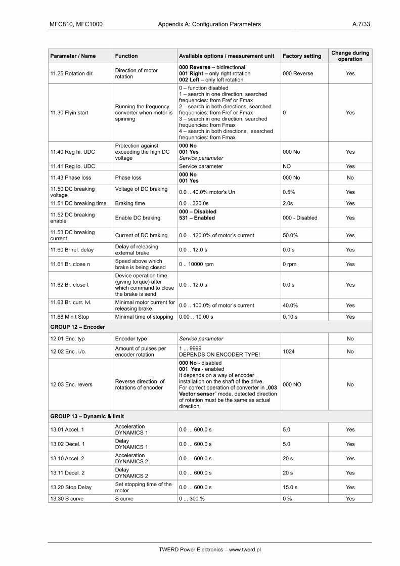
11.25 Rotation dir.Direction of motor rotation
000 Reverse – bidirectional001 Right – only right rotation002 Left – only left rotation
000 Reverse Yes
11.30 Flyin startRunning the frequency converter when motor is spinning
0 – function disabled1 – search in one direction, searched frequencies: from Fref or Fmax2 – search in both directions, searched frequencies: from Fref or Fmax3 – search in one direction, searched frequencies: from Fmax4 – search in both directions, searched frequencies: from Fmax
0 Yes
11.40 Reg hi. UDCProtection against exceeding the high DC voltage
000 No001 YesService parameter
000 No Yes
11.41 Reg lo. UDC Service parameter NO Yes
11.43 Phase loss Phase loss000 No001 Yes
000 No No
11.50 DC breaking voltage
Voltage of DC braking0.0 .. 40.0% motor's Un 0.5% Yes
11.51 DC breaking time Braking time 0.0 .. 320.0s 2.0s Yes
11.52 DC breaking enable
Enable DC braking000 – Disabled531 – Enabled 000 - Disabled Yes
11.53 DC breaking current
Current of DC braking 0.0 .. 120.0% of motor’s current 50.0% Yes
11.60 Br rel. delayDelay of releasing external brake
0.0 .. 12.0 s 0.0 s Yes
11.61 Br. close nSpeed above which brake is being closed
0 .. 10000 rpm 0 rpm Yes
11.62 Br. close t
Device operation time (giving torque) after which command to closethe brake is send
0.0 .. 12.0 s 0.0 s Yes
11.63 Br. curr. lvl. Minimal motor current forreleasing brake
0.0 .. 100.0% of motor’s current 40.0% Yes
11.68 Min t Stop Minimal time of stopping 0.00 .. 10.00 s 0.10 s Yes
GROUP 12 – Encoder
12.01 Enc. typ Encoder type Service parameter No
12.02 Enc .i./o.Amount of pulses per encoder rotation
1 ... 9999 DEPENDS ON ENCODER TYPE!
1024 No
12.03 Enc. reversReverse direction of rotations of encoder
000 No - disabled001 Yes - enabledIt depends on a way of encoder installation on the shaft of the drive.For correct operation of converter in „003 Vector sensor” mode, detected direction of rotation must be the same as actual direction.
000 NO No
GROUP 13 – Dynamic & limit
13.01 Accel. 1AccelerationDYNAMICS 1
0.0 ... 600.0 s 5.0 Yes
13.02 Decel. 1DelayDYNAMICS 1
0.0 ... 600.0 s 5.0 Yes
13.10 Accel. 2AccelerationDYNAMICS 2
0.0 ... 600.0 s 20 s Yes
13.11 Decel. 2DelayDYNAMICS 2
0.0 ... 600.0 s 20 s Yes
13.20 Stop DelaySet stopping time of the motor
0.0 ... 600.0 s 15.0 s Yes
13.30 S curve S curve 0 ... 300 % 0 % Yes
TWERD Power Electronics – www.twerd.pl
A.8/33 Appendix A: Configuration Parameters MFC810, MFC1000
Parameter / Name Function Available options / measurement unit Factory settingChange during
operation
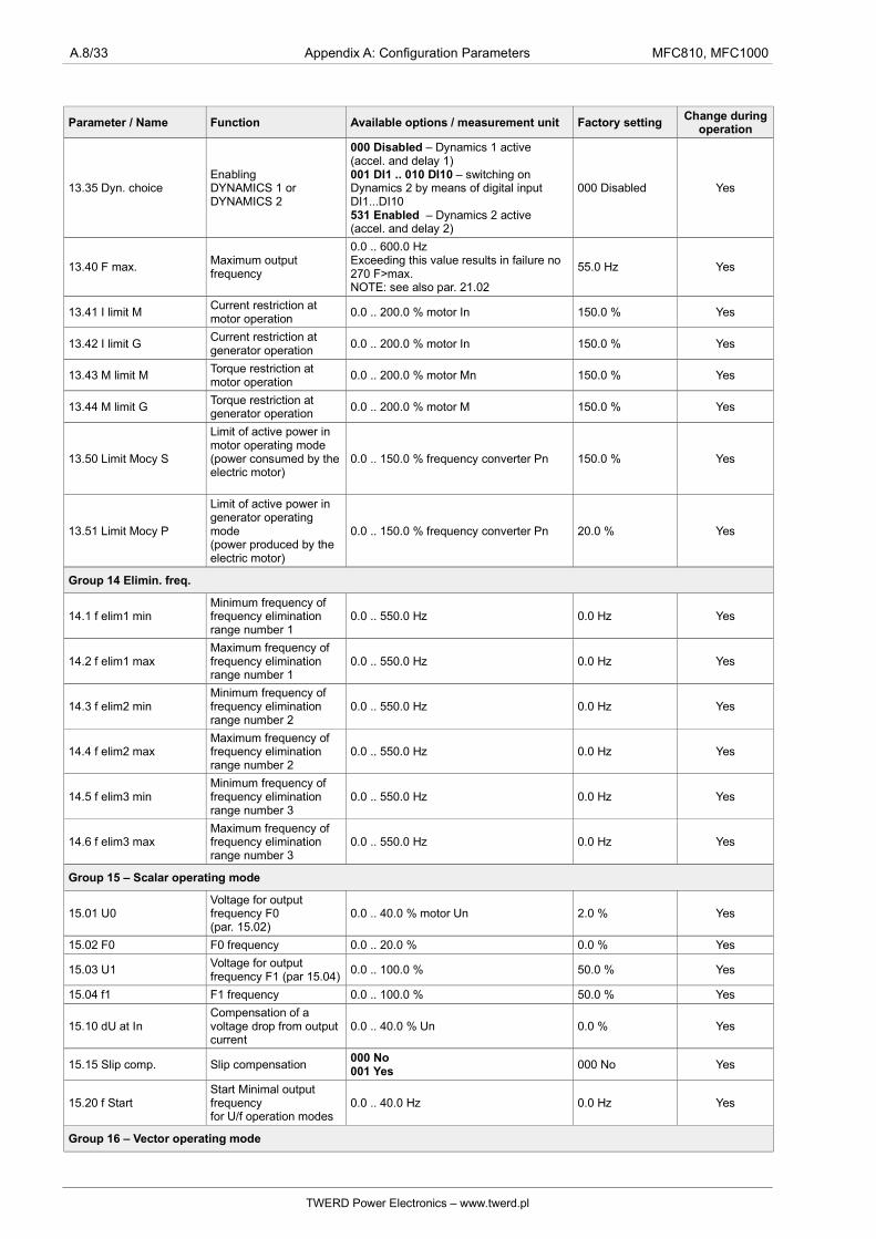
13.35 Dyn. choiceEnablingDYNAMICS 1 or DYNAMICS 2
000 Disabled – Dynamics 1 active(accel. and delay 1)001 DI1 .. 010 DI10 – switching on Dynamics 2 by means of digital input DI1...DI10531 Enabled – Dynamics 2 active(accel. and delay 2)
000 Disabled Yes
13.40 F max.Maximum output frequency
0.0 .. 600.0 HzExceeding this value results in failure no 270 F>max.NOTE: see also par. 21.02
55.0 Hz Yes
13.41 I limit MCurrent restriction at motor operation
0.0 .. 200.0 % motor In 150.0 % Yes
13.42 I limit GCurrent restriction at generator operation
0.0 .. 200.0 % motor In 150.0 % Yes
13.43 M limit MTorque restriction at motor operation
0.0 .. 200.0 % motor Mn 150.0 % Yes
13.44 M limit GTorque restriction at generator operation
0.0 .. 200.0 % motor M 150.0 % Yes
13.50 Limit Mocy S
Limit of active power in motor operating mode(power consumed by theelectric motor)
0.0 .. 150.0 % frequency converter Pn 150.0 % Yes
13.51 Limit Mocy P
Limit of active power in generator operating mode(power produced by the electric motor)
0.0 .. 150.0 % frequency converter Pn 20.0 % Yes
Group 14 Elimin. freq.
14.1 f elim1 minMinimum frequency of frequency elimination range number 1
0.0 .. 550.0 Hz 0.0 Hz Yes
14.2 f elim1 maxMaximum frequency of frequency elimination range number 1
0.0 .. 550.0 Hz 0.0 Hz Yes
14.3 f elim2 minMinimum frequency of frequency elimination range number 2
0.0 .. 550.0 Hz 0.0 Hz Yes
14.4 f elim2 maxMaximum frequency of frequency elimination range number 2
0.0 .. 550.0 Hz 0.0 Hz Yes
14.5 f elim3 minMinimum frequency of frequency elimination range number 3
0.0 .. 550.0 Hz 0.0 Hz Yes
14.6 f elim3 maxMaximum frequency of frequency elimination range number 3
0.0 .. 550.0 Hz 0.0 Hz Yes
Group 15 – Scalar operating mode
15.01 U0Voltage for output frequency F0(par. 15.02)
0.0 .. 40.0 % motor Un 2.0 % Yes
15.02 F0 F0 frequency 0.0 .. 20.0 % 0.0 % Yes
15.03 U1Voltage for output frequency F1 (par 15.04)
0.0 .. 100.0 % 50.0 % Yes
15.04 f1 F1 frequency 0.0 .. 100.0 % 50.0 % Yes
15.10 dU at InCompensation of a voltage drop from output current
0.0 .. 40.0 % Un 0.0 % Yes
15.15 Slip comp. Slip compensation000 No001 Yes
000 No Yes
15.20 f StartStart Minimal output frequencyfor U/f operation modes
0.0 .. 40.0 Hz 0.0 Hz Yes
Group 16 – Vector operating mode
TWERD Power Electronics – www.twerd.pl
MFC810, MFC1000 Appendix A: Configuration Parameters A.9/33
Parameter / Name Function Available options / measurement unit Factory settingChange during
operation
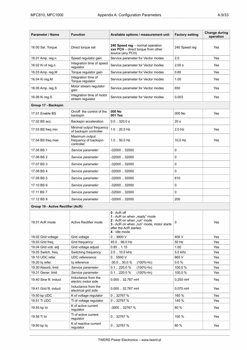
16.00 Sel. Torque Direct torque set240 Speed reg – normal operationxxx PCH – direct torque from other source (any PCH)
240 Speed reg Yes
16.01 Amp. reg.n Speed regulator gain Service parameter for Vector modes 2.0 Yes
16.02 Ki of reg.nIntegration time of speedregulator
Service parameter for Vector modes 2.00 s Yes
16.03 Amp. reg.M Torque regulator gain Service parameter for Vector modes 0.60 Yes
16.04 Ki reg.MIntegration time of Torque regulator
Service parameter for Vector modes 1.00 Yes
16.05 Amp. reg.SMotor stream regulator gain
Service parameter for Vector modes 650 Yes
16.06 Ki reg.SIntegration time of motor stream regulator
Service parameter for Vector modes 0.003 Yes
Group 17 - Backspin
17.01 Enable BSOn/off the control of the backspin
000 No001 Yes
000 No Yes
17.02 BS acc. Backspin acceleration 0.0 .. 320.0 s 20 s
17.03 BS freq minMinimal output frequencyof backspin controller
1.0 .. 20.0 Hz 2.0 Hz Yes
17.04 BS freq maxMaximum output frequency of backspin controller
1.0 .. 50.0 Hz 10.0 Hz Yes
17.05 BS 1 Service parameter -32000 .. 32000 0
17.06 BS 2 Service parameter -32000 .. 32000 0
17.07 BS 3 Service parameter -32000 .. 32000 0
17.08 BS 4 Service parameter -32000 .. 32000 0
17.09 BS 5 Service parameter -32000 .. 32000 610
17.10 BS 6 Service parameter -32000 .. 32000 0
17.11 BS 7 Service parameter -32000 .. 32000 0
17.12 BS 8 Service parameter -32000 .. 32000 200
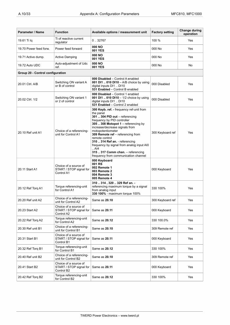
Group 19 - Active Rectifier (AcR)
19.01 AcR mode Active Rectifier mode
0 - AcR off1 - AcR on when „ready” mode2 - AcR on when „run” mode3 - AcR on when „run” mode, motor startsafter the AcR started.4 - Idle mode
0 Yes
19.02 Grid voltage Grid voltage 0 .. 3800 V 400 V Yes
19.03 Grid freq. Grid frequency 45.0 .. 66.0 Hz 50 Hz Yes
19.04 Grid volt. adj Grid voltage adjust 0.85 .. 1.15 1.00 Yes
19.05 Switch. freq. Switching frequency 2.0 .. 10.0 kHz 5.0 kHz Yes
19.10 UDC refer. UDC refererence 0 .. 5500 V 665 V Yes
19.20 Iq refer. Iq reference -30.0 .. 30.0 % (100%=In) 0.0 % Yes
19.30 Absorb. limit Service parameter 0.1 .. 220.0 % (100%=In) 100,0 % Yes
19.31 Gener. limit Service parameter 0.1 .. 220.0 % (100%=In) 100,0 % Yes
19.40 Sine fil. inductInductance from the electric motor side
0.000 .. 32.767 mH 0.250 mH Yes
19.41 Grid fil. inductInductance from the electrical grid side
0.000 .. 32.767 mH 0.070 mH Yes
19.50 kp UDC K of voltage regulator 0 .. 32767 % 160 % Yes
19.51 Ti UDC Ti of voltage regulator 0 .. 32767 % 140 % Yes
19.55 kp IdK of active current regulator
-3000 .. 32767 % 80 % Yes
19.56 Ti IdTi of active current regulator
0 .. 32767 % 100 % Yes
19.60 kp IqK of reactive current regulator
0 .. 32767 % 80 % Yes
TWERD Power Electronics – www.twerd.pl
A.10/33 Appendix A: Configuration Parameters MFC810, MFC1000
Parameter / Name Function Available options / measurement unit Factory settingChange during
operation
19.61 Ti IqTi of reactive current regulator
0 .. 32767 100 % Yes
19.70 Power feed forw. Power feed forward000 NO001 YES
000 No Yes
19.71 Active dump. Active Damping000 NO001 YES
000 No Yes
19.72 Auto UDCAuto-adjustment of Udc ref.
000 NO001 YES
000 No No
Group 20 - Control configuration
20.01 Ctrl. A/BSwitching ON variant A or B of control
000 Disabled – Control A enabled001 DI1 .. 010 DI10 – A/B choice by usingdigital inputs DI1 .. DI10531 Enabled – Control B enabled
000 Disabled Yes
20.02 Ctrl. 1/2Switching ON variant 1 or 2 of control
000 Disabled – Control 1 enabled001 DI1 .. 010 DI10 – 1/2 choice by usingdigital inputs DI1 .. DI10531 Enabled – Control 2 enabled
000 Disabled Yes
20.10 Ref unit A1Choice of a referencing-unit for Control A1
300 Keyb. ref. - frequency ref-unit from the panel301 .. 304 PID out – referencing frequency by PID controller305 .. 308 Motopot 1 – referencing by increase/decrease signals from motopotentiometer309 Remote ref – referencing from remote control310 .. 314 Ref an. - referencing frequency by signal from analog input AI0.. AI4 315 .. 317 Comm chan. – referencing frequency from communication channel
300 Keyboard ref Yes
20.11 Start A1Choice of a source of START / STOP signal forControl A1
000 Keyboard001 RS002 Remote 1003 Remote 2004 Remote 3005 Remote 4
000 Keyboard Yes
20.12 Ref Torq A1Torque referencing-unit for Control A1
310 .. 314 , 320 .. 329 Ref an. - referencing maximum torque by a signal from analog input330 100% - maximum torque 100%
330 100% Yes
20.20 Ref unit A2Choice of a referencing-unit for Control A2
Same as 20.10 300 Keyboard ref Yes
20.23 Start A2Choice of a source of START / STOP signal forControl A2
Same as 20.11 000 Keyboard Yes
20.22 Ref Torq A2Torque referencing-unit for Control A2
Same as 20.12 330 100.0% Yes
20.30 Ref unit B1Choice of a referencing-unit for Control B1
Same as 20.10 309 Remote ref Yes
20.31 Start B1Choice of a source of START / STOP signal forControl B1
Same as 20.11 000 Keyboard Yes
20.32 Ref Torq B1Torque referencing-unit for Control B1
Same as 20.12 330 100% Yes
20.40 Ref unit B2Choice of a referencing-unit for Control B2
Same as 20.10 309 Remote ref Yes
20.41 Start B2Choice of a source of START / STOP signal forControl B2
Same as 20.11 000 Keyboard Yes
20.42 Ref Torq B2Torque referencing-unit for Control B2
Same as 20.12 330 100% Yes
TWERD Power Electronics – www.twerd.pl
MFC810, MFC1000 Appendix A: Configuration Parameters A.11/33
Parameter / Name Function Available options / measurement unit Factory settingChange during
operation
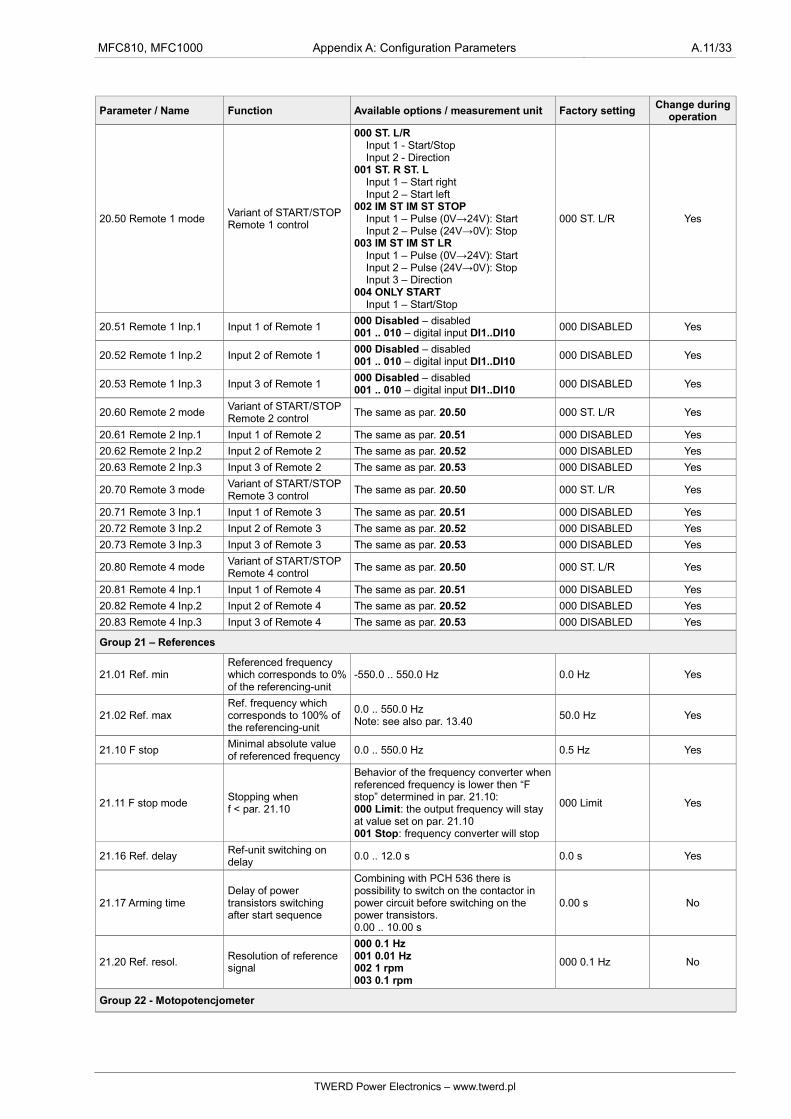
20.50 Remote 1 modeVariant of START/STOP Remote 1 control
000 ST. L/R Input 1 - Start/Stop Input 2 - Direction001 ST. R ST. L Input 1 – Start right Input 2 – Start left002 IM ST IM ST STOP Input 1 – Pulse (0V→24V): Start Input 2 – Pulse (24V→0V): Stop003 IM ST IM ST LR Input 1 – Pulse (0V→24V): Start Input 2 – Pulse (24V→0V): Stop Input 3 – Direction004 ONLY START Input 1 – Start/Stop
000 ST. L/R Yes
20.51 Remote 1 Inp.1 Input 1 of Remote 1 000 Disabled – disabled001 .. 010 – digital input DI1..DI10
000 DISABLED Yes
20.52 Remote 1 Inp.2 Input 2 of Remote 1 000 Disabled – disabled001 .. 010 – digital input DI1..DI10
000 DISABLED Yes
20.53 Remote 1 Inp.3 Input 3 of Remote 1000 Disabled – disabled001 .. 010 – digital input DI1..DI10
000 DISABLED Yes
20.60 Remote 2 modeVariant of START/STOP Remote 2 control
The same as par. 20.50 000 ST. L/R Yes
20.61 Remote 2 Inp.1 Input 1 of Remote 2 The same as par. 20.51 000 DISABLED Yes
20.62 Remote 2 Inp.2 Input 2 of Remote 2 The same as par. 20.52 000 DISABLED Yes
20.63 Remote 2 Inp.3 Input 3 of Remote 2 The same as par. 20.53 000 DISABLED Yes
20.70 Remote 3 modeVariant of START/STOP Remote 3 control
The same as par. 20.50 000 ST. L/R Yes
20.71 Remote 3 Inp.1 Input 1 of Remote 3 The same as par. 20.51 000 DISABLED Yes
20.72 Remote 3 Inp.2 Input 2 of Remote 3 The same as par. 20.52 000 DISABLED Yes
20.73 Remote 3 Inp.3 Input 3 of Remote 3 The same as par. 20.53 000 DISABLED Yes
20.80 Remote 4 modeVariant of START/STOP Remote 4 control
The same as par. 20.50 000 ST. L/R Yes
20.81 Remote 4 Inp.1 Input 1 of Remote 4 The same as par. 20.51 000 DISABLED Yes
20.82 Remote 4 Inp.2 Input 2 of Remote 4 The same as par. 20.52 000 DISABLED Yes
20.83 Remote 4 Inp.3 Input 3 of Remote 4 The same as par. 20.53 000 DISABLED Yes
Group 21 – References
21.01 Ref. minReferenced frequency which corresponds to 0%of the referencing-unit
-550.0 .. 550.0 Hz 0.0 Hz Yes
21.02 Ref. maxRef. frequency which corresponds to 100% of the referencing-unit
0.0 .. 550.0 HzNote: see also par. 13.40
50.0 Hz Yes
21.10 F stopMinimal absolute value of referenced frequency
0.0 .. 550.0 Hz 0.5 Hz Yes
21.11 F stop modeStopping when f < par. 21.10
Behavior of the frequency converter whenreferenced frequency is lower then “F stop” determined in par. 21.10:000 Limit: the output frequency will stay at value set on par. 21.10001 Stop: frequency converter will stop
000 Limit Yes
21.16 Ref. delayRef-unit switching on delay
0.0 .. 12.0 s 0.0 s Yes
21.17 Arming timeDelay of power transistors switching after start sequence
Combining with PCH 536 there is possibility to switch on the contactor in power circuit before switching on the power transistors.0.00 .. 10.00 s
0.00 s No
21.20 Ref. resol.Resolution of reference signal
000 0.1 Hz001 0.01 Hz002 1 rpm003 0.1 rpm
000 0.1 Hz No
Group 22 - Motopotencjometer
TWERD Power Electronics – www.twerd.pl

A.12/33 Appendix A: Configuration Parameters MFC810, MFC1000
Parameter / Name Function Available options / measurement unit Factory settingChange during
operation
22.01 Mtp1 adr up
Source of “increase” signal for Motopotentiometer 1 referencing-unit
000 Disabled001 DI1 .. 010 DI10 - increase ref.-unit, when there is a voltage supplied on digital input DI1 .. DI10
000 Disabled Yes
22.02 Mtp1 adr down
Source of “decrease” signal for Motopotentiometer 1 referencing-unit
000 Disabled001 DI1 .. 010 DI10 - decrease ref.-unit, when there is a voltage supplied on digital input DI1 .. DI10
000 Disabled Yes
22.03 Motopot1 modeMotopotentiometer 1 mode
000 – sending STOP signal (by pushing STOP button, through RS or other possibilities) causes resetting of motopotentiometer settings.
001 – value of motopotentiometer setting is stored in memory. There is no possibility of changing this setting during stoppage.
002 – value of current referencing-unit setting traced by motopotentiometer. Applied for gentle transmission from current ref.-unit to motopotentiometer
003 – value of motopotentiometer setting stored in the memory. There is a possibility of changing this setting during stoppage.
Note:000, 001, 002: modes applied when current ref.-unit (par. 20.10, 20.20, 20.30,20.40) is set on Motopot 1 .. Motopot 4003: mode independent of current ref.-unit choice
002 Refer. traced Yes
22.04 Motopot1 time
Time of increase/decrease of Motopotentiometer 1 referencing-unit
0.0 .. 320.0 s 10.0 s Yes
22.11 Mtp2 adr up
Source of “increase” signal for Motopotentiometer 2 referencing-unit
The same as par. 22.01See par. 22.01
000 Disabled Yes
22.12 Mtp2 adr down
Source of “decrease” signal for Motopotentiometer 2 referencing-unit
The same as par. 22.02See par. 22.02
000 Disabled Yes
22.13 Motopot2 modeMotopotentiometer 2 mode
The same as par. 22.03See par. 22.03
002 Refer. traced Yes
22.14 Motopot2 time
Time of increase/decrease of Motopotentiometer 2 referencing-unit
The same as par. 22.04See par. 22.04
10.0 s Yes
22.23 Mtp3 adr up
Source of “increase” signal for Motopotentiometer 3 referencing-unit
The same as par. 22.01See par. 22.01
000 Disabled Yes
22.22 Mtp3 adr down
Source of “decrease” signal for Motopotentiometer 3 referencing-unit
The same as par. 22.02See par. 22.02
000 Disabled Yes
22.23 Motopot3 modeMotopotentiometer 3 mode
The same as par. 22.03See par. 22.03
002 Refer. traced Yes
22.24 Motopot3 time
Time of increase/decrease of Motopotentiometer 3 referencing-unit
The same as par. 22.04See par. 22.04
10.0 s Yes
22.31 Mtp4 adr up
Source of “increase” signal for Motopotentiometer 4 referencing-unit
The same as par. 22.01See par. 22.01
000 Disabled Yes
TWERD Power Electronics – www.twerd.pl

MFC810, MFC1000 Appendix A: Configuration Parameters A.13/33
Parameter / Name Function Available options / measurement unit Factory settingChange during
operation
22.32 Mtp4 adr down
Source of “decrease” signal for Motopotentiometer 4 referencing-unit
The same as par. 22.02See par. 22.02
000 Disabled Yes
22.33 Motopot4 modeMotopotentiometer 4 mode
The same as par. 22.03See par. 22.03
002 Refer. traced Yes
22.34 Motopot4 time
Time of increase/decrease of Motopotentiometer 4 referencing-unit
The same as par. 22.04See par. 22.04
10.0 s Yes
Group 23 - Const. speed
23.01 Adr const 0Source of signal for referencing Constant 0 speeds
000 Disabled - Off001 DI1 .. 010 DI10 - On when there is a voltage supplied on digital inputDI1 .. DI10531 Yes – always On
000 Disabled Yes
23.02 Adr const 1Source of signal for referencing Constant 1 speeds
The same as par. 23.01 000 Disabled Yes
23.03 Adr const 2Source of signal for referencing Constant 2 speeds
The same as par. 23.01 000 Disabled Yes
23.04 Adr const 3Source of signal for referencing Constant 3 speeds
The same as par. 23.01 000 Disabled Yes
23.06 Const 1 Constant frequency 1 -550.0 .. 500.0 Hz 10.0 Hz Yes
23.07 Const 2 Constant frequency 2 -550.0 .. 500.0 Hz 20.0 Hz Yes
23.08 Const 3 Constant frequency 3 -550.0 .. 500.0 Hz 25.0 Hz Yes
23.09 Const 4 Constant frequency 4 -550.0 .. 500.0 Hz 30.0 Hz Yes
23.10 Const 5 Constant frequency 5 -550.0 .. 500.0 Hz 40.0 Hz Yes
23.11 Const 6 Constant frequency 6 -550.0 .. 500.0 Hz 45.0 Hz Yes
23.12 Const 7 Constant frequency 7 -550.0 .. 500.0 Hz 50.0 Hz Yes
23.13 Const 8 Constant frequency 8 -550.0 .. 500.0 Hz 50.0 Hz Yes
23.14 Const 9 Constant frequency 9 -550.0 .. 500.0 Hz 50.0 Hz Yes
23.15 Const 10 Constant frequency 10 -550.0 .. 500.0 Hz 50.0 Hz Yes
23.16 Const 11 Constant frequency 11 -550.0 .. 500.0 Hz 50.0 Hz Yes
23.17 Const 12 Constant frequency 12 -550.0 .. 500.0 Hz 50.0 Hz Yes
23.18 Const 13 Constant frequency 13 -550.0 .. 500.0 Hz 50.0 Hz Yes
23.19 Const 14 Constant frequency 14 -550.0 .. 500.0 Hz 50.0 Hz Yes
23.20 Const 15 Constant frequency 15 -550.0 .. 500.0 Hz 50.0 Hz Yes
Group 24 - Analog in.
24.01 Cfg. A0 inpConfiguration of analog input AI0
000 0-10 V: 0V=0%, 10V=100%001 10-0 V: 10V=100%, 0V=0%002 2-10 V: 2V=0%, 10V=100%
000 0-10 V Yes
24.02 Scale A0 inpScale of analog referencing-unit Ref. AI0
-500.0 .. 500.0 % 100.0% Yes
24.03 Offs. A0 inpOffset of analog referencing-unit Ref. AI0
-500.0 .. 500.0 % 0.0 % Yes
24.04 Filter A0 inpConstant of time of lowpass AI0 filter
0.00 .. 50.00 s 0.10 s Yes
24.11 Cfg. A1 inpConfiguration of analog input AI1
000 0-10 V: 0V=0%, 10V=100%001 10-0 V: 10V=100%, 0V=0%002 2-10 V: 2V=0%, 10V=100%003 10-2 V: 10V=100%, 2V=0%004 0-20 mA: 0mA=0%, 20mA=100%005 20-0 mA: 20mA=100%, 0mA=0%006 4-20mA: 4mA=0%, 20mA=100%007 20-4 mA: 20mA=100%, 4mA=0%
000 0-10 V Yes
24.12 Scale A1 inpScale of analog referencing-unit Ref. AI1
-500.0 .. 500.0 % 100.0% Yes
24.13 Offs. A1 inpOffset of analog referencing-unit Ref. AI1
-500.0 .. 500.0 % 0.0 % Yes
24.14 Filter A1 inpConstant of time of lowpass AI1 filter
0.00 .. 50.00 s 0.10 s Yes
TWERD Power Electronics – www.twerd.pl

A.14/33 Appendix A: Configuration Parameters MFC810, MFC1000
Parameter / Name Function Available options / measurement unit Factory settingChange during
operation
24.23 Cfg. A2 inpConfiguration of analog input AI2
The same as par. 24.11 000 0-10 V Yes
24.22 Scale A2 inpScale of analog referencing-unit Ref. AI2
-500.0 .. 500.0 % 100.0% Yes
24.23 Offs. A2 inpOffset of analog referencing-unit Ref. AI2
-500.0..500.0 % 0.0 % Yes
24.24 Filter A2 inpConstant of time of lowpass AI2 filter
0.00 .. 50.00 s 0.10 s Yes
24.31 Cfg. A3 inpConfiguration of analog input AI3
The same as par. 24.11 000 0-10 V Yes
24.32 Scale A3 inpScale of analog referencing-unit Ref. AI3
-500.0..500.0 % 100.0% Yes
24.33 Offs. A3 inpOffset of analog referencing-unit Ref. AI3
-500.0 .. 500.0 % 0.0 % Yes
24.34 Filter A3 inpConstant of time of lowpass AI3 filter
0.00 .. 50.00 s 0.10 s Yes
24.41 Cfg. A4 inpConfiguration of analog input AI4
The same as par. 24.11 000 0-10 V Yes
24.42 Scale A4 inpScale of analog referencing-unit Ref. AI4
-500.0 .. 500.0 % 100% Yes
24.43 Offs. A4 inpOffset of analog referencing-unit Ref. AI4
-500.0 .. 500.0 % 0% Yes
24.44 Filter A4 inpConstant of time of lowpass AI4 filter
0.00 .. 50.00 s 0.10 s Yes
Group 25 - Analog out.
25.01 Cfg. A1 outConfiguration of analog output AO1
000 0-10V: 0V=0%, 10V=100%001 10-0 V: 10V=0%, 0V=100%002 2-10 V: 2V=0%, 10V=100%003 10-2 V: 10V=0%, 2V=100%004 0-20 mA: 0mA=0%, 20mA=100%005 20-0 mA: 20mA=0%, 0mA=100%006 4-20 mA: 4mA=0%, 20mA=100%007 20-4 mA: 20mA=0%, 4mA=100%
000 0-10V Yes
25.02 Src. A1 outChoice of signal for analog output AO1
230 Rotation %
speed with a sign0.0 % = -Nn,50.0 % = 0,100.0 % = nn
231 Out freq %
output frequency100.0 % = fn
232 Ref freq %
reference frequency100.0 % = fn
233 Curr % output current100.0 % = In
234 Torq % load with a sign100.0 % = 2Mn,50.0 % = 0,0.0 % = -2Mn
235 Power % Output power %236 Drive volt%
Output voltage %
230 Rotation % Yes
25.03 Scale A1 outScale of analog output AO1
0.0 .. 500.0 % 100 % Yes
25.04 Offset A1 outOffset of analog output AO1
-500.0 .. 500.0 0,0 % Yes
25.05 Filter A1 outConstant of time of lowpass AO1 filter
0.00 .. 50.00 0.10 Yes
25.11 Cfg. A2 outConfiguration of analog output AO2
The same as par. 25.01 000 0-10V Yes
25.12 Src. A2 outChoice of signal for analog output AO2
The same as par. 25.02 232 Ref freq % Yes
25.13 Scale A2 outScale of analog output AO2
0.0 .. 500.0 % 100.0 % Yes
25.14 Offset A2 outOffset of analog output AO2
-500.0 .. 500.0 0.0 % Yes
25.15 Filter A2 outConstant of time of lowpass AO2 filter
0.00 .. 50.00 0.10 s Yes
TWERD Power Electronics – www.twerd.pl

MFC810, MFC1000 Appendix A: Configuration Parameters A.15/33
Parameter / Name Function Available options / measurement unit Factory settingChange during
operation
Group 26 - Digital inputs
26.01 Op. perm.External operation permission
000 Denied – operation denied001 Input 1 .. 010 Input 10 – operation allowed when there is a voltage supplied on digital input DI1 .. DI10531 Enabled - operation allowed
531 Allowed Yes
26.02 Op. block.External operation blocking
000 Disabled - without operation blocking001 Input 1 .. 010 Input 10 - blocking active, when there is voltage supplied ondigital inputs DI1 .. DI10
000 Disabled Yes
26.03 Em. stop Emergency Stop
000 Disabled - no possibility of emergency stopping001 Input 1 .. 010 Input 10 - emergency stop by one of a digital inputs DI1 .. DI10
000 Disabled Yes
26.10 Enable ACREnable active rectifier AcR
000 Denied - Off001 DI1 .. 010 DI10 - On when there is a voltage supplied on digital inputsDI1 .. DI10531 Allowed - always On
000 Denied Yes
26.11 Ext. reset Source of external reset
000 Disabled - no possibility of external erasing a fault message001 Input 1 .. 010 Input 10 - erasing a fault by digital inputs DI1 .. DI10
000 Disabled Yes
Group 27 - Digital outputs: 1 - 16
27.01 F thresh. 1 Threshold frequency 1 0.0 .. 550.0 Hz 25.0 Hz Yes
27.02 F thresh. 2 Threshold frequency 2 0.0 .. 550.0 Hz 45.0 Hz Yes
27.03 Temp.1 minMinimum of temperature 1 (PCH 524)
0 .. 120 0C 50 0C Yes
27.04 Temp.1 maxMaximum of temperature 1 (PCH 524)
0 .. 120 0C 75 0C Yes
27.05 Temp.2 minMinimum of temperature 2 (PCH 525)
0 .. 120 0C 37 0C Yes
27.06 Temp.2 maxMaximum of temperature 2 (PCH 525)
0 .. 120 0C 40 0C Yes
27.10 PT100 1 minMinimum temperature of PT100 1 (PCH 528)
-200.0 .. 800.0 0C 0 0C Yes
27.11 PT100 1 max Maximum temperature ofPT100 1 (PCH 528)
-200.0 .. 800.0 0C 0 0C Yes
27.12 PT100 2 minMinimum temperature of PT100 2 (PCH 529)
-200.0 .. 800.0 0C 0 0C Yes
27.13 PT100 2 maxMaximum temperature ofPT100 2 (PCH 529)
-200.0 .. 800.0 0C 0 0C Yes
TWERD Power Electronics – www.twerd.pl
A.16/33 Appendix A: Configuration Parameters MFC810, MFC1000
Parameter / Name Function Available options / measurement unit Factory settingChange during
operation
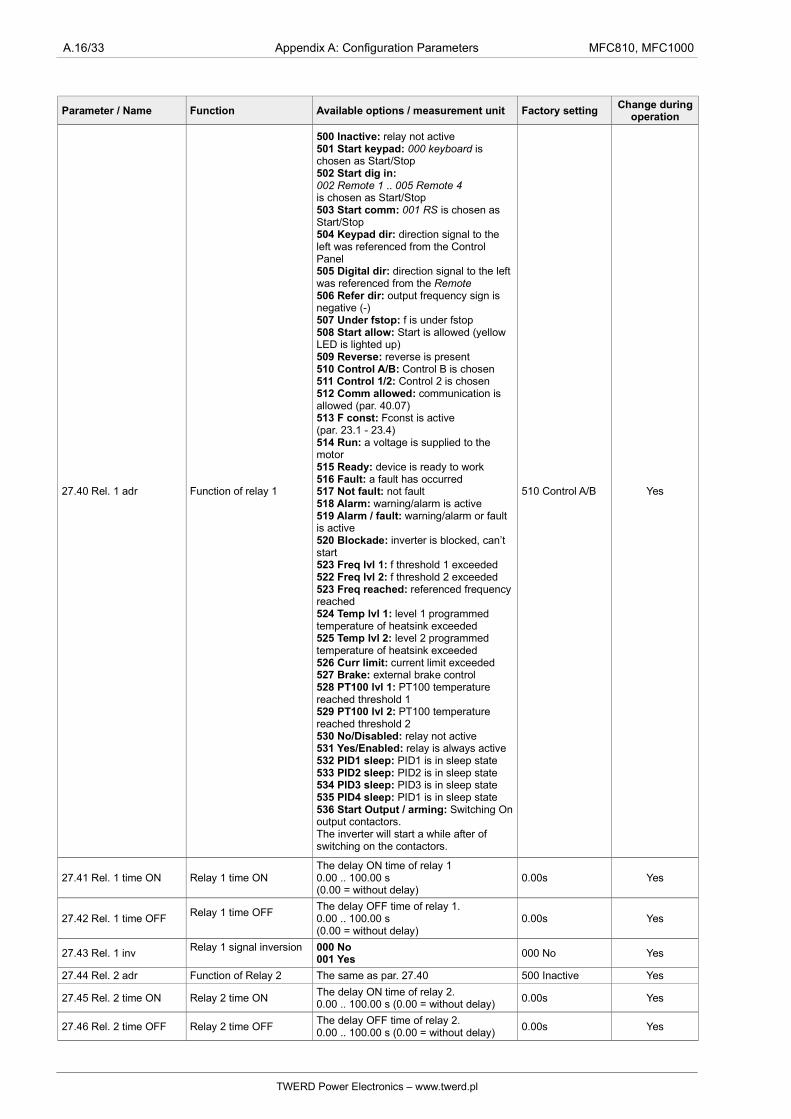
27.40 Rel. 1 adr Function of relay 1
500 Inactive: relay not active501 Start keypad: 000 keyboard is chosen as Start/Stop502 Start dig in:002 Remote 1 .. 005 Remote 4 is chosen as Start/Stop503 Start comm: 001 RS is chosen as Start/Stop504 Keypad dir: direction signal to the left was referenced from the Control Panel505 Digital dir: direction signal to the left was referenced from the Remote506 Refer dir: output frequency sign is negative (-)507 Under fstop: f is under fstop508 Start allow: Start is allowed (yellow LED is lighted up)509 Reverse: reverse is present510 Control A/B: Control B is chosen511 Control 1/2: Control 2 is chosen512 Comm allowed: communication is allowed (par. 40.07)513 F const: Fconst is active(par. 23.1 - 23.4)514 Run: a voltage is supplied to the motor515 Ready: device is ready to work516 Fault: a fault has occurred517 Not fault: not fault518 Alarm: warning/alarm is active519 Alarm / fault: warning/alarm or fault is active520 Blockade: inverter is blocked, can’t start523 Freq lvl 1: f threshold 1 exceeded522 Freq lvl 2: f threshold 2 exceeded523 Freq reached: referenced frequencyreached524 Temp lvl 1: level 1 programmed temperature of heatsink exceeded525 Temp lvl 2: level 2 programmed temperature of heatsink exceeded526 Curr limit: current limit exceeded527 Brake: external brake control528 PT100 lvl 1: PT100 temperature reached threshold 1529 PT100 lvl 2: PT100 temperature reached threshold 2530 No/Disabled: relay not active531 Yes/Enabled: relay is always active532 PID1 sleep: PID1 is in sleep state533 PID2 sleep: PID2 is in sleep state534 PID3 sleep: PID3 is in sleep state535 PID4 sleep: PID1 is in sleep state536 Start Output / arming: Switching Onoutput contactors.The inverter will start a while after of switching on the contactors.
510 Control A/B Yes
27.41 Rel. 1 time ON Relay 1 time ONThe delay ON time of relay 10.00 .. 100.00 s (0.00 = without delay)
0.00s Yes
27.42 Rel. 1 time OFFRelay 1 time OFF
The delay OFF time of relay 1.0.00 .. 100.00 s(0.00 = without delay)
0.00s Yes
27.43 Rel. 1 invRelay 1 signal inversion 000 No
001 Yes000 No Yes
27.44 Rel. 2 adr Function of Relay 2 The same as par. 27.40 500 Inactive Yes
27.45 Rel. 2 time ON Relay 2 time ONThe delay ON time of relay 2.0.00 .. 100.00 s (0.00 = without delay)
0.00s Yes
27.46 Rel. 2 time OFF Relay 2 time OFFThe delay OFF time of relay 2.0.00 .. 100.00 s (0.00 = without delay)
0.00s Yes
TWERD Power Electronics – www.twerd.pl
MFC810, MFC1000 Appendix A: Configuration Parameters A.17/33
Parameter / Name Function Available options / measurement unit Factory settingChange during
operation
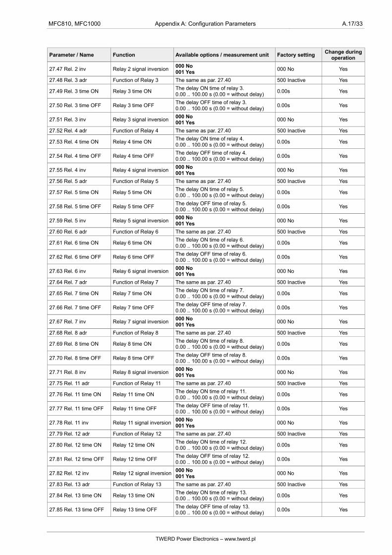
27.47 Rel. 2 inv Relay 2 signal inversion000 No001 Yes
000 No Yes
27.48 Rel. 3 adr Function of Relay 3 The same as par. 27.40 500 Inactive Yes
27.49 Rel. 3 time ON Relay 3 time ONThe delay ON time of relay 3.0.00 .. 100.00 s (0.00 = without delay)
0.00s Yes
27.50 Rel. 3 time OFF Relay 3 time OFFThe delay OFF time of relay 3.0.00 .. 100.00 s (0.00 = without delay)
0.00s Yes
27.51 Rel. 3 inv Relay 3 signal inversion000 No001 Yes
000 No Yes
27.52 Rel. 4 adr Function of Relay 4 The same as par. 27.40 500 Inactive Yes
27.53 Rel. 4 time ON Relay 4 time ONThe delay ON time of relay 4.0.00 .. 100.00 s (0.00 = without delay)
0.00s Yes
27.54 Rel. 4 time OFF Relay 4 time OFFThe delay OFF time of relay 4.0.00 .. 100.00 s (0.00 = without delay)
0.00s Yes
27.55 Rel. 4 inv Relay 4 signal inversion000 No001 Yes
000 No Yes
27.56 Rel. 5 adr Function of Relay 5 The same as par. 27.40 500 Inactive Yes
27.57 Rel. 5 time ON Relay 5 time ONThe delay ON time of relay 5.0.00 .. 100.00 s (0.00 = without delay)
0.00s Yes
27.58 Rel. 5 time OFF Relay 5 time OFFThe delay OFF time of relay 5.0.00 .. 100.00 s (0.00 = without delay)
0.00s Yes
27.59 Rel. 5 inv Relay 5 signal inversion000 No001 Yes
000 No Yes
27.60 Rel. 6 adr Function of Relay 6 The same as par. 27.40 500 Inactive Yes
27.61 Rel. 6 time ON Relay 6 time ONThe delay ON time of relay 6.0.00 .. 100.00 s (0.00 = without delay)
0.00s Yes
27.62 Rel. 6 time OFF Relay 6 time OFFThe delay OFF time of relay 6.0.00 .. 100.00 s (0.00 = without delay)
0.00s Yes
27.63 Rel. 6 inv Relay 6 signal inversion000 No001 Yes
000 No Yes
27.64 Rel. 7 adr Function of Relay 7 The same as par. 27.40 500 Inactive Yes
27.65 Rel. 7 time ON Relay 7 time ONThe delay ON time of relay 7.0.00 .. 100.00 s (0.00 = without delay)
0.00s Yes
27.66 Rel. 7 time OFF Relay 7 time OFFThe delay OFF time of relay 7.0.00 .. 100.00 s (0.00 = without delay)
0.00s Yes
27.67 Rel. 7 inv Relay 7 signal inversion000 No001 Yes
000 No Yes
27.68 Rel. 8 adr Function of Relay 8 The same as par. 27.40 500 Inactive Yes
27.69 Rel. 8 time ON Relay 8 time ONThe delay ON time of relay 8.0.00 .. 100.00 s (0.00 = without delay)
0.00s Yes
27.70 Rel. 8 time OFF Relay 8 time OFFThe delay OFF time of relay 8.0.00 .. 100.00 s (0.00 = without delay)
0.00s Yes
27.71 Rel. 8 inv Relay 8 signal inversion000 No001 Yes
000 No Yes
27.75 Rel. 11 adr Function of Relay 11 The same as par. 27.40 500 Inactive Yes
27.76 Rel. 11 time ON Relay 11 time ONThe delay ON time of relay 11.0.00 .. 100.00 s (0.00 = without delay)
0.00s Yes
27.77 Rel. 11 time OFF Relay 11 time OFFThe delay OFF time of relay 11.0.00 .. 100.00 s (0.00 = without delay)
0.00s Yes
27.78 Rel. 11 inv Relay 11 signal inversion000 No001 Yes
000 No Yes
27.79 Rel. 12 adr Function of Relay 12 The same as par. 27.40 500 Inactive Yes
27.80 Rel. 12 time ON Relay 12 time ONThe delay ON time of relay 12.0.00 .. 100.00 s (0.00 = without delay)
0.00s Yes
27.81 Rel. 12 time OFF Relay 12 time OFFThe delay OFF time of relay 12.0.00 .. 100.00 s (0.00 = without delay)
0.00s Yes
27.82 Rel. 12 inv Relay 12 signal inversion000 No001 Yes
000 No Yes
27.83 Rel. 13 adr Function of Relay 13 The same as par. 27.40 500 Inactive Yes
27.84 Rel. 13 time ON Relay 13 time ONThe delay ON time of relay 13.0.00 .. 100.00 s (0.00 = without delay)
0.00s Yes
27.85 Rel. 13 time OFF Relay 13 time OFFThe delay OFF time of relay 13.0.00 .. 100.00 s (0.00 = without delay)
0.00s Yes
TWERD Power Electronics – www.twerd.pl
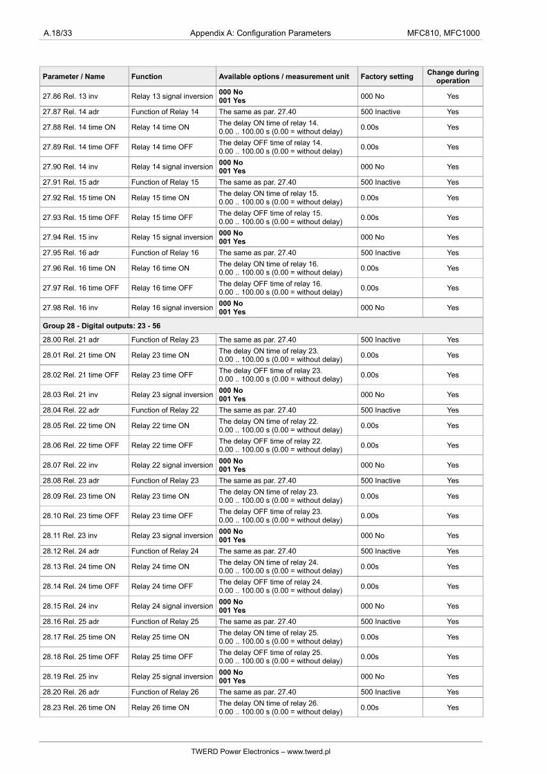
A.18/33 Appendix A: Configuration Parameters MFC810, MFC1000
Parameter / Name Function Available options / measurement unit Factory settingChange during
operation
27.86 Rel. 13 inv Relay 13 signal inversion000 No001 Yes
000 No Yes
27.87 Rel. 14 adr Function of Relay 14 The same as par. 27.40 500 Inactive Yes
27.88 Rel. 14 time ON Relay 14 time ONThe delay ON time of relay 14.0.00 .. 100.00 s (0.00 = without delay)
0.00s Yes
27.89 Rel. 14 time OFF Relay 14 time OFFThe delay OFF time of relay 14.0.00 .. 100.00 s (0.00 = without delay)
0.00s Yes
27.90 Rel. 14 inv Relay 14 signal inversion000 No001 Yes
000 No Yes
27.91 Rel. 15 adr Function of Relay 15 The same as par. 27.40 500 Inactive Yes
27.92 Rel. 15 time ON Relay 15 time ONThe delay ON time of relay 15.0.00 .. 100.00 s (0.00 = without delay)
0.00s Yes
27.93 Rel. 15 time OFF Relay 15 time OFFThe delay OFF time of relay 15.0.00 .. 100.00 s (0.00 = without delay)
0.00s Yes
27.94 Rel. 15 inv Relay 15 signal inversion000 No001 Yes
000 No Yes
27.95 Rel. 16 adr Function of Relay 16 The same as par. 27.40 500 Inactive Yes
27.96 Rel. 16 time ON Relay 16 time ONThe delay ON time of relay 16.0.00 .. 100.00 s (0.00 = without delay)
0.00s Yes
27.97 Rel. 16 time OFF Relay 16 time OFFThe delay OFF time of relay 16.0.00 .. 100.00 s (0.00 = without delay)
0.00s Yes
27.98 Rel. 16 inv Relay 16 signal inversion000 No001 Yes
000 No Yes
Group 28 - Digital outputs: 23 - 56
28.00 Rel. 21 adr Function of Relay 23 The same as par. 27.40 500 Inactive Yes
28.01 Rel. 21 time ON Relay 23 time ONThe delay ON time of relay 23.0.00 .. 100.00 s (0.00 = without delay)
0.00s Yes
28.02 Rel. 21 time OFF Relay 23 time OFFThe delay OFF time of relay 23.0.00 .. 100.00 s (0.00 = without delay)
0.00s Yes
28.03 Rel. 21 inv Relay 23 signal inversion000 No001 Yes
000 No Yes
28.04 Rel. 22 adr Function of Relay 22 The same as par. 27.40 500 Inactive Yes
28.05 Rel. 22 time ON Relay 22 time ONThe delay ON time of relay 22.0.00 .. 100.00 s (0.00 = without delay)
0.00s Yes
28.06 Rel. 22 time OFF Relay 22 time OFFThe delay OFF time of relay 22.0.00 .. 100.00 s (0.00 = without delay)
0.00s Yes
28.07 Rel. 22 inv Relay 22 signal inversion000 No001 Yes
000 No Yes
28.08 Rel. 23 adr Function of Relay 23 The same as par. 27.40 500 Inactive Yes
28.09 Rel. 23 time ON Relay 23 time ONThe delay ON time of relay 23.0.00 .. 100.00 s (0.00 = without delay)
0.00s Yes
28.10 Rel. 23 time OFF Relay 23 time OFFThe delay OFF time of relay 23.0.00 .. 100.00 s (0.00 = without delay)
0.00s Yes
28.11 Rel. 23 inv Relay 23 signal inversion000 No001 Yes
000 No Yes
28.12 Rel. 24 adr Function of Relay 24 The same as par. 27.40 500 Inactive Yes
28.13 Rel. 24 time ON Relay 24 time ONThe delay ON time of relay 24.0.00 .. 100.00 s (0.00 = without delay)
0.00s Yes
28.14 Rel. 24 time OFF Relay 24 time OFFThe delay OFF time of relay 24.0.00 .. 100.00 s (0.00 = without delay)
0.00s Yes
28.15 Rel. 24 inv Relay 24 signal inversion000 No001 Yes
000 No Yes
28.16 Rel. 25 adr Function of Relay 25 The same as par. 27.40 500 Inactive Yes
28.17 Rel. 25 time ON Relay 25 time ONThe delay ON time of relay 25.0.00 .. 100.00 s (0.00 = without delay)
0.00s Yes
28.18 Rel. 25 time OFF Relay 25 time OFFThe delay OFF time of relay 25.0.00 .. 100.00 s (0.00 = without delay)
0.00s Yes
28.19 Rel. 25 inv Relay 25 signal inversion000 No001 Yes
000 No Yes
28.20 Rel. 26 adr Function of Relay 26 The same as par. 27.40 500 Inactive Yes
28.23 Rel. 26 time ON Relay 26 time ONThe delay ON time of relay 26.0.00 .. 100.00 s (0.00 = without delay)
0.00s Yes
TWERD Power Electronics – www.twerd.pl
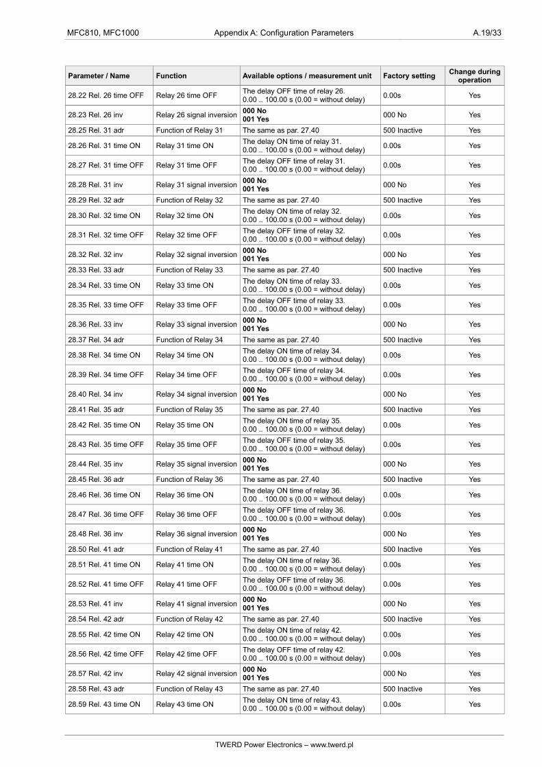
MFC810, MFC1000 Appendix A: Configuration Parameters A.19/33
Parameter / Name Function Available options / measurement unit Factory settingChange during
operation
28.22 Rel. 26 time OFF Relay 26 time OFFThe delay OFF time of relay 26.0.00 .. 100.00 s (0.00 = without delay)
0.00s Yes
28.23 Rel. 26 inv Relay 26 signal inversion000 No001 Yes
000 No Yes
28.25 Rel. 31 adr Function of Relay 31 The same as par. 27.40 500 Inactive Yes
28.26 Rel. 31 time ON Relay 31 time ONThe delay ON time of relay 31.0.00 .. 100.00 s (0.00 = without delay)
0.00s Yes
28.27 Rel. 31 time OFF Relay 31 time OFFThe delay OFF time of relay 31.0.00 .. 100.00 s (0.00 = without delay)
0.00s Yes
28.28 Rel. 31 inv Relay 31 signal inversion000 No001 Yes
000 No Yes
28.29 Rel. 32 adr Function of Relay 32 The same as par. 27.40 500 Inactive Yes
28.30 Rel. 32 time ON Relay 32 time ONThe delay ON time of relay 32.0.00 .. 100.00 s (0.00 = without delay)
0.00s Yes
28.31 Rel. 32 time OFF Relay 32 time OFFThe delay OFF time of relay 32.0.00 .. 100.00 s (0.00 = without delay)
0.00s Yes
28.32 Rel. 32 inv Relay 32 signal inversion000 No001 Yes
000 No Yes
28.33 Rel. 33 adr Function of Relay 33 The same as par. 27.40 500 Inactive Yes
28.34 Rel. 33 time ON Relay 33 time ONThe delay ON time of relay 33.0.00 .. 100.00 s (0.00 = without delay)
0.00s Yes
28.35 Rel. 33 time OFF Relay 33 time OFFThe delay OFF time of relay 33.0.00 .. 100.00 s (0.00 = without delay)
0.00s Yes
28.36 Rel. 33 inv Relay 33 signal inversion000 No001 Yes
000 No Yes
28.37 Rel. 34 adr Function of Relay 34 The same as par. 27.40 500 Inactive Yes
28.38 Rel. 34 time ON Relay 34 time ONThe delay ON time of relay 34.0.00 .. 100.00 s (0.00 = without delay)
0.00s Yes
28.39 Rel. 34 time OFF Relay 34 time OFFThe delay OFF time of relay 34.0.00 .. 100.00 s (0.00 = without delay)
0.00s Yes
28.40 Rel. 34 inv Relay 34 signal inversion000 No001 Yes
000 No Yes
28.41 Rel. 35 adr Function of Relay 35 The same as par. 27.40 500 Inactive Yes
28.42 Rel. 35 time ON Relay 35 time ONThe delay ON time of relay 35.0.00 .. 100.00 s (0.00 = without delay)
0.00s Yes
28.43 Rel. 35 time OFF Relay 35 time OFFThe delay OFF time of relay 35.0.00 .. 100.00 s (0.00 = without delay)
0.00s Yes
28.44 Rel. 35 inv Relay 35 signal inversion000 No001 Yes
000 No Yes
28.45 Rel. 36 adr Function of Relay 36 The same as par. 27.40 500 Inactive Yes
28.46 Rel. 36 time ON Relay 36 time ONThe delay ON time of relay 36.0.00 .. 100.00 s (0.00 = without delay)
0.00s Yes
28.47 Rel. 36 time OFF Relay 36 time OFFThe delay OFF time of relay 36.0.00 .. 100.00 s (0.00 = without delay)
0.00s Yes
28.48 Rel. 36 inv Relay 36 signal inversion000 No001 Yes
000 No Yes
28.50 Rel. 41 adr Function of Relay 41 The same as par. 27.40 500 Inactive Yes
28.51 Rel. 41 time ON Relay 41 time ONThe delay ON time of relay 36.0.00 .. 100.00 s (0.00 = without delay)
0.00s Yes
28.52 Rel. 41 time OFF Relay 41 time OFFThe delay OFF time of relay 36.0.00 .. 100.00 s (0.00 = without delay)
0.00s Yes
28.53 Rel. 41 inv Relay 41 signal inversion000 No001 Yes
000 No Yes
28.54 Rel. 42 adr Function of Relay 42 The same as par. 27.40 500 Inactive Yes
28.55 Rel. 42 time ON Relay 42 time ONThe delay ON time of relay 42.0.00 .. 100.00 s (0.00 = without delay)
0.00s Yes
28.56 Rel. 42 time OFF Relay 42 time OFFThe delay OFF time of relay 42.0.00 .. 100.00 s (0.00 = without delay)
0.00s Yes
28.57 Rel. 42 inv Relay 42 signal inversion000 No001 Yes
000 No Yes
28.58 Rel. 43 adr Function of Relay 43 The same as par. 27.40 500 Inactive Yes
28.59 Rel. 43 time ON Relay 43 time ONThe delay ON time of relay 43.0.00 .. 100.00 s (0.00 = without delay)
0.00s Yes
TWERD Power Electronics – www.twerd.pl

A.20/33 Appendix A: Configuration Parameters MFC810, MFC1000
Parameter / Name Function Available options / measurement unit Factory settingChange during
operation
28.60 Rel. 43 time OFF Relay 43 time OFFThe delay OFF time of relay 43.0.00 .. 100.00 s (0.00 = without delay)
0.00s Yes
28.61 Rel. 43 inv Relay 43 signal inversion000 No001 Yes
000 No Yes
28.62 Rel. 44 adr Function of Relay 44 The same as par. 27.40 500 Inactive Yes
28.63 Rel. 44 time ON Relay 44 time ONThe delay ON time of relay 44.0.00 .. 100.00 s (0.00 = without delay)
0.00s Yes
28.64 Rel. 44 time OFF Relay 44 time OFFThe delay OFF time of relay 44.0.00 .. 100.00 s (0.00 = without delay)
0.00s Yes
28.65 Rel. 44 inv Relay 44 signal inversion000 No001 Yes
000 No Yes
28.66 Rel. 45 adr Function of Relay 45 The same as par. 27.40 500 Inactive Yes
28.67 Rel. 45 time ON Relay 45 time ONThe delay ON time of relay 45.0.00 .. 100.00 s (0.00 = without delay)
0.00s Yes
28.68 Rel. 45 time OFF Relay 45 time OFFThe delay OFF time of relay 45.0.00 .. 100.00 s (0.00 = without delay)
0.00s Yes
28.69 Rel. 45 inv Relay 45 signal inversion000 No001 Yes
000 No Yes
28.70 Rel. 46 adr Function of Relay 46 The same as par. 27.40 500 Inactive Yes
28.71 Rel. 46 time ON Relay 46 time ONThe delay ON time of relay 46.0.00 .. 100.00 s (0.00 = without delay)
0.00s Yes
28.72 Rel. 46 time OFF Relay 46 time OFFThe delay OFF time of relay 46.0.00 .. 100.00 s (0.00 = without delay)
0.00s Yes
28.73 Rel. 46 inv Relay 46 signal inversion000 No001 Yes
000 No Yes
28.75 Rel. 51 adr Function of Relay 51 The same as par. 27.40 500 Inactive Yes
28.76 Rel. 51 time ON Relay 51 time ONThe delay ON time of relay 51.0.00 .. 100.00 s (0.00 = without delay)
0.00s Yes
28.77 Rel. 51 time OFF Relay 51 time OFFThe delay OFF time of relay 51.0.00 .. 100.00 s (0.00 = without delay)
0.00s Yes
28.78 Rel. 51 inv Relay 51 signal inversion000 No001 Yes
000 No Yes
28.79 Rel. 52 adr Function of Relay 52 The same as par. 27.40 500 Inactive Yes
28.80 Rel. 52 time ON Relay 52 time ONThe delay ON time of relay 52.0.00 .. 100.00 s (0.00 = without delay)
0.00s Yes
28.81 Rel. 52 time OFF Relay 52 time OFFThe delay OFF time of relay 52.0.00 .. 100.00 s (0.00 = without delay)
0.00s Yes
28.82 Rel. 52 inv Relay 52 signal inversion000 No001 Yes
000 No Yes
28.83 Rel. 53 adr Function of Relay 53 The same as par. 27.40 500 Inactive Yes
28.84 Rel. 53 time ON Relay 53 time ONThe delay ON time of relay 53.0.00 .. 100.00 s (0.00 = without delay)
0.00s Yes
28.85 Rel. 53 time OFF Relay 53 time OFFThe delay OFF time of relay 53.0.00 .. 100.00 s (0.00 = without delay)
0.00s Yes
28.86 Rel. 53 inv Relay 53 signal inversion000 No001 Yes
000 No Yes
28.87 Rel. 54 adr Function of Relay 54 The same as par. 27.40 500 Inactive Yes
28.88 Rel. 54 time ON Relay 54 time ONThe delay ON time of relay 54.0.00 .. 100.00 s (0.00 = without delay)
0.00s Yes
28.89 Rel. 54 time OFF Relay 54 time OFFThe delay OFF time of relay 54.0.00 .. 100.00 s (0.00 = without delay)
0.00s Yes
28.90 Rel. 54 inv Relay 54 signal inversion000 No001 Yes
000 No Yes
28.91 Rel. 55 adr Function of Relay 55 The same as par. 27.40 500 Inactive Yes
28.92 Rel. 55 time ON Relay 55 time ONThe delay ON time of relay 55.0.00 .. 100.00 s (0.00 = without delay)
0.00s Yes
28.93 Rel. 55 time OFF Relay 55 time OFFThe delay OFF time of relay 55.0.00 .. 100.00 s (0.00 = without delay)
0.00s Yes
28.94 Rel. 55 inv Relay 55 signal inversion000 No001 Yes
000 No Yes
28.95 Rel. 56 adr Function of Relay 56 The same as par. 27.40 500 Inactive Yes
28.96 Rel. 56 time ON Relay 56 time ONThe delay ON time of relay 56.0.00 .. 100.00 s (0.00 = without delay)
0.00s Yes
TWERD Power Electronics – www.twerd.pl
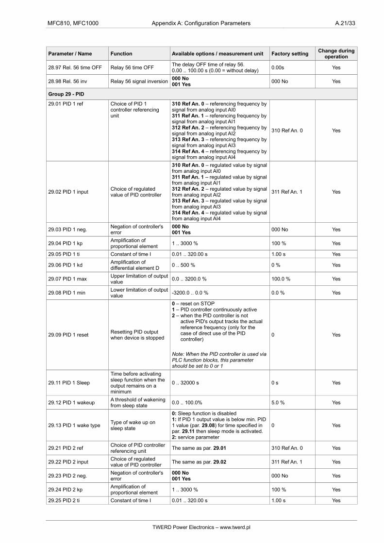
MFC810, MFC1000 Appendix A: Configuration Parameters A.21/33
Parameter / Name Function Available options / measurement unit Factory settingChange during
operation
28.97 Rel. 56 time OFF Relay 56 time OFFThe delay OFF time of relay 56.0.00 .. 100.00 s (0.00 = without delay)
0.00s Yes
28.98 Rel. 56 inv Relay 56 signal inversion000 No001 Yes
000 No Yes
Group 29 - PID
29.01 PID 1 ref Choice of PID 1 controller referencing unit
310 Ref An. 0 – referencing frequency bysignal from analog input AI0311 Ref An. 1 – referencing frequency bysignal from analog input AI1312 Ref An. 2 – referencing frequency bysignal from analog input AI2313 Ref An. 3 – referencing frequency bysignal from analog input AI3314 Ref An. 4 – referencing frequency bysignal from analog input AI4
310 Ref An. 0 Yes
29.02 PID 1 inputChoice of regulated value of PID controller
310 Ref An. 0 – regulated value by signalfrom analog input AI0311 Ref An. 1 – regulated value by signalfrom analog input AI1312 Ref An. 2 – regulated value by signalfrom analog input AI2313 Ref An. 3 – regulated value by signalfrom analog input AI3314 Ref An. 4 – regulated value by signalfrom analog input AI4
311 Ref An. 1 Yes
29.03 PID 1 neg.Negation of controller's error
000 No001 Yes
000 No Yes
29.04 PID 1 kpAmplification of proportional element
1 .. 3000 % 100 % Yes
29.05 PID 1 ti Constant of time I 0.01 .. 320.00 s 1.00 s Yes
29.06 PID 1 kdAmplification of differential element D
0 .. 500 % 0 % Yes
29.07 PID 1 maxUpper limitation of outputvalue
0.0 .. 3200.0 % 100.0 % Yes
29.08 PID 1 minLower limitation of outputvalue
-3200.0 .. 0.0 % 0.0 % Yes
29.09 PID 1 resetResetting PID output when device is stopped
0 – reset on STOP1 – PID controller continuously active2 – when the PID controller is not active PID's output tracks the actual reference frequency (only for the case of direct use of the PID controller)
Note: When the PID controller is used viaPLC function blocks, this parameter should be set to 0 or 1
0 Yes
29.11 PID 1 Sleep
Time before activating sleep function when the output remains on a minimum
0 .. 32000 s 0 s Yes
29.12 PID 1 wakeupA threshold of wakening from sleep state
0.0 .. 100.0% 5.0 % Yes
29.13 PID 1 wake typeType of wake up on sleep state
0: Sleep function is disabled1: If PID 1 output value is below min. PID 1 value (par. 29.08) for time specified in par. 29.11 then sleep mode is activated.2: service parameter
0 Yes
29.21 PID 2 refChoice of PID controller referencing unit
The same as par. 29.01 310 Ref An. 0 Yes
29.22 PID 2 inputChoice of regulated value of PID controller
The same as par. 29.02 311 Ref An. 1 Yes
29.23 PID 2 neg.Negation of controller's error
000 No001 Yes
000 No Yes
29.24 PID 2 kpAmplification of proportional element
1 .. 3000 % 100 % Yes
29.25 PID 2 ti Constant of time I 0.01 .. 320.00 s 1.00 s Yes
TWERD Power Electronics – www.twerd.pl
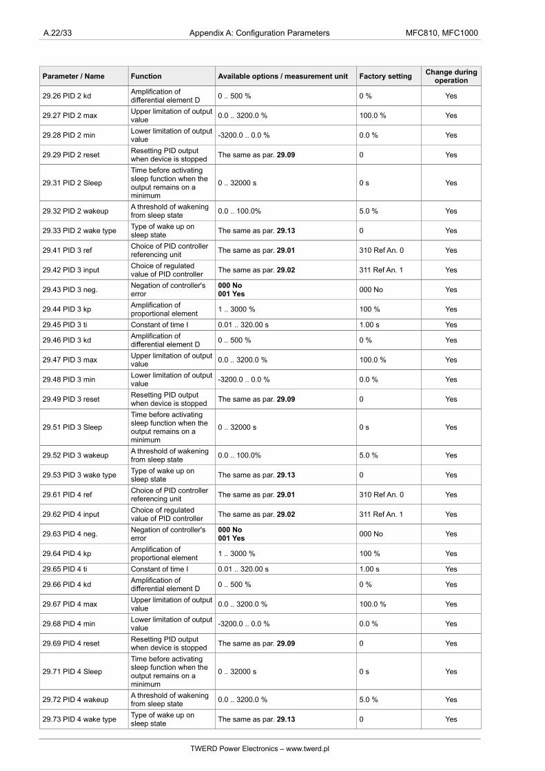
A.22/33 Appendix A: Configuration Parameters MFC810, MFC1000
Parameter / Name Function Available options / measurement unit Factory settingChange during
operation
29.26 PID 2 kdAmplification of differential element D
0 .. 500 % 0 % Yes
29.27 PID 2 maxUpper limitation of outputvalue
0.0 .. 3200.0 % 100.0 % Yes
29.28 PID 2 minLower limitation of outputvalue
-3200.0 .. 0.0 % 0.0 % Yes
29.29 PID 2 resetResetting PID output when device is stopped
The same as par. 29.09 0 Yes
29.31 PID 2 Sleep
Time before activating sleep function when the output remains on a minimum
0 .. 32000 s 0 s Yes
29.32 PID 2 wakeupA threshold of wakening from sleep state
0.0 .. 100.0% 5.0 % Yes
29.33 PID 2 wake typeType of wake up on sleep state
The same as par. 29.13 0 Yes
29.41 PID 3 refChoice of PID controller referencing unit
The same as par. 29.01 310 Ref An. 0 Yes
29.42 PID 3 inputChoice of regulated value of PID controller
The same as par. 29.02 311 Ref An. 1 Yes
29.43 PID 3 neg.Negation of controller's error
000 No001 Yes
000 No Yes
29.44 PID 3 kpAmplification of proportional element
1 .. 3000 % 100 % Yes
29.45 PID 3 ti Constant of time I 0.01 .. 320.00 s 1.00 s Yes
29.46 PID 3 kdAmplification of differential element D
0 .. 500 % 0 % Yes
29.47 PID 3 maxUpper limitation of outputvalue
0.0 .. 3200.0 % 100.0 % Yes
29.48 PID 3 minLower limitation of outputvalue
-3200.0 .. 0.0 % 0.0 % Yes
29.49 PID 3 resetResetting PID output when device is stopped
The same as par. 29.09 0 Yes
29.51 PID 3 Sleep
Time before activating sleep function when the output remains on a minimum
0 .. 32000 s 0 s Yes
29.52 PID 3 wakeupA threshold of wakening from sleep state
0.0 .. 100.0% 5.0 % Yes
29.53 PID 3 wake typeType of wake up on sleep state
The same as par. 29.13 0 Yes
29.61 PID 4 refChoice of PID controller referencing unit
The same as par. 29.01 310 Ref An. 0 Yes
29.62 PID 4 inputChoice of regulated value of PID controller
The same as par. 29.02 311 Ref An. 1 Yes
29.63 PID 4 neg.Negation of controller's error
000 No001 Yes
000 No Yes
29.64 PID 4 kpAmplification of proportional element
1 .. 3000 % 100 % Yes
29.65 PID 4 ti Constant of time I 0.01 .. 320.00 s 1.00 s Yes
29.66 PID 4 kdAmplification of differential element D
0 .. 500 % 0 % Yes
29.67 PID 4 maxUpper limitation of outputvalue
0.0 .. 3200.0 % 100.0 % Yes
29.68 PID 4 minLower limitation of outputvalue
-3200.0 .. 0.0 % 0.0 % Yes
29.69 PID 4 resetResetting PID output when device is stopped
The same as par. 29.09 0 Yes
29.71 PID 4 Sleep
Time before activating sleep function when the output remains on a minimum
0 .. 32000 s 0 s Yes
29.72 PID 4 wakeupA threshold of wakening from sleep state
0.0 .. 3200.0 % 5.0 % Yes
29.73 PID 4 wake typeType of wake up on sleep state
The same as par. 29.13 0 Yes
TWERD Power Electronics – www.twerd.pl

MFC810, MFC1000 Appendix A: Configuration Parameters A.23/33
Parameter / Name Function Available options / measurement unit Factory settingChange during
operation
Group 30 - Motor protect.
30.01 Therm. faultResponse to thermistor fault
000 None - no response001 Warning - a warning will be displayed002 Fault - device will stop and message will be displayed
000 None Yes
30.02 Therm. source Thermistor source
000 Disabled – disabled001 Input 1 .. 010 Input 10 – digital signal for thermistor123 An. Inp 1 .. 124 An. Inp 4 - analog input for thermistor
30.10 I2T block.Switching on blocking from thermal overload
000 No - disabled001 Yes - enabled
001 Yes Yes
30.11 I therm.Setting of drive thermal protection current
0.0 .. 200.0 % 100.0 % Yes
30.12 I therm. 0Setting of thermorelay for stopped drive
0.0 .. 200.0 % 50.0 % Yes
30.13 Therm. const.Constant of el. motor heating 0 .. 200 min 2 min Yes
30.25 Motor existReaction to motor exist.
If motor current is lower than percentage of nominal motor current during specified time after start, reaction will be applied:000 None - no response001 Warning - a warning will be displayed002 Fault - device will stop and message will be displayed
000 None Yes
30.26 Motor ex. curr. Percentage of motor nominal current
10 .. 100 % 10 % Yes
30.27 Motor ex. time Motor exist check time 0.1s .. 10.0 s 0.5 s Yes
30.35 I groundValue of leakage current at which device will be shut down
10.0 .. 100.0 % 30.0 % Yes
30.37 Low DC Service parameter 200 .. 1000 V 200 V Yes
30.40 Re.Sym. lackResponse to asymmetry of the load
000 None - no response001 Warning - a warning will be displayed002 Fault - device will stop and message will be displayed
000 None Yes
30.45 Re. underload Response to underload
000 None - no response001 Warning - a warning will be displayed002 Fault - device will stop and message will be displayed
000 None Yes
30.46 Underl. time Time of underload 0 .. 1200s 0 s Yes
30.47 Underl. torque Torque of underload 0.0 .. 100.0 % 0.0 % Yes
30.50 Stall re.Response to stall of the drive
000 None - no response001 Warning - a warning will be displayed002 Fault - device will stop and message will be displayed
000 None Yes
30.51 Stall freq. Stall frequency 0.0 .. 30 0 Hz 0.0 Hz Yes
30.52 Stall time Stall time 0 .. 600 s 0 s Yes
30.60 Speed err re.Response to error of output speed
000 None - no response001 Warning - a warning will be displayed002 Fault - device will stop and message will be displayed
000 None Yes
30.61 Delta n-nz
Acceptable difference between referenced speed and speed of the el. motor.
0 .. 500 rpm 0 rpm Yes
30.62 D time max.Maximum time of acceptable error
0.0 .. 12.0 s 0.0 s Yes
TWERD Power Electronics – www.twerd.pl
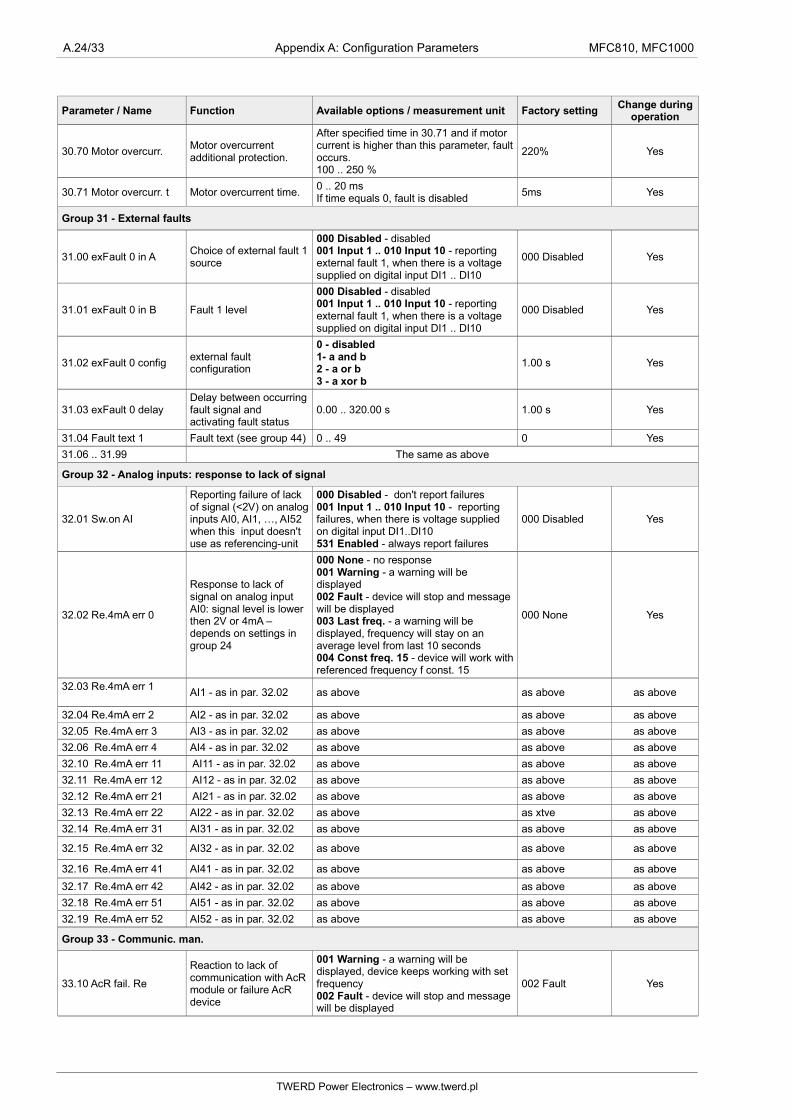
A.24/33 Appendix A: Configuration Parameters MFC810, MFC1000
Parameter / Name Function Available options / measurement unit Factory settingChange during
operation
30.70 Motor overcurr.Motor overcurrent additional protection.
After specified time in 30.71 and if motor current is higher than this parameter, faultoccurs.100 .. 250 %
220% Yes
30.71 Motor overcurr. t Motor overcurrent time.0 .. 20 msIf time equals 0, fault is disabled
5ms Yes
Group 31 - External faults
31.00 exFault 0 in AChoice of external fault 1source
000 Disabled - disabled001 Input 1 .. 010 Input 10 - reporting external fault 1, when there is a voltage supplied on digital input DI1 .. DI10
000 Disabled Yes
31.01 exFault 0 in B Fault 1 level
000 Disabled - disabled001 Input 1 .. 010 Input 10 - reporting external fault 1, when there is a voltage supplied on digital input DI1 .. DI10
000 Disabled Yes
31.02 exFault 0 configexternal fault configuration
0 - disabled1- a and b2 - a or b3 - a xor b
1.00 s Yes
31.03 exFault 0 delayDelay between occurringfault signal and activating fault status
0.00 .. 320.00 s 1.00 s Yes
31.04 Fault text 1 Fault text (see group 44) 0 .. 49 0 Yes
31.06 .. 31.99 The same as above
Group 32 - Analog inputs: response to lack of signal
32.01 Sw.on AI
Reporting failure of lack of signal (<2V) on analoginputs AI0, AI1, T, AI52 when this input doesn't use as referencing-unit
000 Disabled - don't report failures001 Input 1 .. 010 Input 10 - reporting failures, when there is voltage supplied on digital input DI1..DI10531 Enabled - always report failures
000 Disabled Yes
32.02 Re.4mA err 0
Response to lack of signal on analog input AI0: signal level is lower then 2V or 4mA – depends on settings in group 24
000 None - no response001 Warning - a warning will be displayed002 Fault - device will stop and message will be displayed 003 Last freq. - a warning will be displayed, frequency will stay on an average level from last 10 seconds004 Const freq. 15 - device will work withreferenced frequency f const. 15
000 None Yes
32.03 Re.4mA err 1AI1 - as in par. 32.02 as above as above as above
32.04 Re.4mA err 2 AI2 - as in par. 32.02 as above as above as above
32.05 Re.4mA err 3 AI3 - as in par. 32.02 as above as above as above
32.06 Re.4mA err 4 AI4 - as in par. 32.02 as above as above as above
32.10 Re.4mA err 11 AI11 - as in par. 32.02 as above as above as above
32.11 Re.4mA err 12 AI12 - as in par. 32.02 as above as above as above
32.12 Re.4mA err 21 AI21 - as in par. 32.02 as above as above as above
32.13 Re.4mA err 22 AI22 - as in par. 32.02 as above as xtve as above
32.14 Re.4mA err 31 AI31 - as in par. 32.02 as above as above as above
32.15 Re.4mA err 32 AI32 - as in par. 32.02 as above as above as above
32.16 Re.4mA err 41 AI41 - as in par. 32.02 as above as above as above
32.17 Re.4mA err 42 AI42 - as in par. 32.02 as above as above as above
32.18 Re.4mA err 51 AI51 - as in par. 32.02 as above as above as above
32.19 Re.4mA err 52 AI52 - as in par. 32.02 as above as above as above
Group 33 - Communic. man.
33.10 AcR fail. Re
Reaction to lack of communication with AcR module or failure AcR device
001 Warning - a warning will be displayed, device keeps working with set frequency002 Fault - device will stop and message will be displayed
002 Fault Yes
TWERD Power Electronics – www.twerd.pl

MFC810, MFC1000 Appendix A: Configuration Parameters A.25/33
Parameter / Name Function Available options / measurement unit Factory settingChange during
operation
33.11 Re. RS lackResponse to lack of communication through RS link
000 None - no response001 Warning - a warning will be displayed002 Fault - device will stop and message will be displayed 003 Last freq. - a warning will be displayed, frequency will stay on an average level from last 10s004 Const freq. 15 - device will work withreferenced frequency f const. 15
000 None Yes
33.12 Rs lackAcceptable time of lack of communication through RS link
0 .. 600 s 30 s Yes
33.50 Re. key lack
Response to lack of keyboard (only for referencing from keyboard)
The same as par. 33.11 000 None Yes
33.51 Key lack timeAcceptable time of lack of keyboard
0 .. 300 s 30 s Yes
Group 34 - Other man.
34.01 R breaking tMaximum operate resistor's time in DC voltage
0.00 .. 650.00 s 5.00 s Yes
34.02 Re. RbrakeReaction to the excess braking time
000 None - no response001 Warning - a warning will be displayed002 Fault - device will stop and messagewill be displayed
001 WarningYes
34.03 R break powerPower of breaking resistors
0.00 - 650.00 kW 0 Yes
34.04 R break resisResistance of breaking resistors
0.00 - 650.00 ohm 0 Yes
Group 35 Autorestarts
35.01 AR. numberMax number of automatic restarts
0 - no restarts1 ... 6 – number of restarts in time determined by par 35.02
0 YES
35.02 AR. time Time of restarts 0 ... 1200.0 s 60 s YES
35.03 AR. delay Restart delay 0.0 ... 10.0 s 1.0 s YES
35.04 AR.low UdcAutomatic restart after Low Udc failure
NO - no restartYES - permission
NO YES
35.05 AR.hi.UdcAutomatic restart after High Udc failure
NO - no restartYES - permission
NO YES
35.06 AR.hi.IAutomatic restart after High Current failure
NO - no restartYES - permission
NO YES
35.07 AR.hi.temp.Automatic restart after High temperature of the heatsink failure
NO - no restartYES - permission
NO YES
Group 40 Unit control
40.01 Par. block Parameters blocking
000 No : modification of parameters is unblocked001 Yes : modification of parameters is blocked
000 No Yes
40.03 LanguageLanguage of the Control Panel
000 English001 Polish
000 English Yes
40.04 Default param. Load default parameters 1 1 No
40.05 Enable EEPROMAccess to save changes in EEPROM memory
000 No : Switching on blocking of writing to EEPROM memory (parameters can bechanged, however they won't be remembered after shut down of power)001 Yes : parameters are normally writtento EEPROM (the access level Lvl2 is necessary)
001 Yes Yes
40.06 Full PCHFull list of Characteristic Points (PCH) are available
000 No001 Yes : values of parameters which arepointers (e.g. par. 40.07) are possible to change in full range PCH.000...PCH.999
000 No Yes
TWERD Power Electronics – www.twerd.pl

A.26/33 Appendix A: Configuration Parameters MFC810, MFC1000
Parameter / Name Function Available options / measurement unit Factory settingChange during
operation
40.07 Enable RS
Permission to control converter through RS communication: e.g. Start/Stop
000 Denied001 Input 1 .. 010 Input 10531 AllowedNote: without this permission you can connect with the frequency inverter and read/save parameters, but you cannot control the drive
531 Allowed Yes
40.11 Unit numberIdentification number of device
1 .. 247 12 Yes
Group 41
41.00 Scr. 1 number Service parameter 1 .. 4 3 Yes
41.01 Scr. 2 number Service parameter 1 .. 4 3
41.02 Scr. 3 number Service parameter 1 .. 4 3
41.10 1.1 start type Service parameter 0 0
41.11 1.1 start Service parameter All parameters from group Monitor 00.03F out
41.12 1.2 start type Service parameter 0 0
41.13 1.2 start Service parameter All parameters from group Monitor 00.06Motor curr
41.14 1.3 start type Service parameter 0 0
41.15 1.3 start Service parameter All parameters from group Monitor 00.05Mot torque
41.16 1.4 start type Service parameter 0 0
41.17 1.4 start Service parameter All parameters from group Monitor 00.00
41.18 1.1 stop type Service parameter 0 0
41.19 1.1 stop Service parameter All parameters from group Monitor 000.03F out
41.20 1.2 stop type Service parameter 0 0
41.23 1.2 stop Service parameter All parameters from group Monitor 00.06Motor curr
41.22 1.3 stop type Service parameter 0 0
41.23 1.3 stop Service parameter All parameters from group Monitor 00.05Mot torque
41.24 1.4 stop type Service parameter 0 0
41.25 1.4 stop Service parameter All parameters from group Monitor 00.00
41.30 2.1 type Service parameter 0 0
41.31 2.1 Service parameter All parameters from group Monitor 00.13Ia curr.
41.32 2.2 type Service parameter 0 0
41.33 2.2 Service parameter All parameters from group Monitor 00.14Ib curr
41.34 2.3 type Service parameter 0 0
41.35 2.3 Service parameter All parameters from group Monitor 00.15Ic curr
41.36 2.4 type Service parameter 0 0
41.37 2.4 Service parameter All parameters from group Monitor 00.00
41.40 3.1 type Service parameter 0 0
41.41 3.1 Service parameter All parameters from group Monitor 01.01Motor n
41.42 3.2 type Service parameter 0 0
41.43 3.2 Service parameter All parameters from group Monitor 01.05Mot torque
41.44 3.3 type Service parameter 0 0
41.45 3.3 Service parameter All parameters from group Monitor01.09Output power
41.46 3.4 type Service parameter 0 0
41.47 3.4 Service parameter All parameters from group Monitor 00.00
TWERD Power Electronics – www.twerd.pl
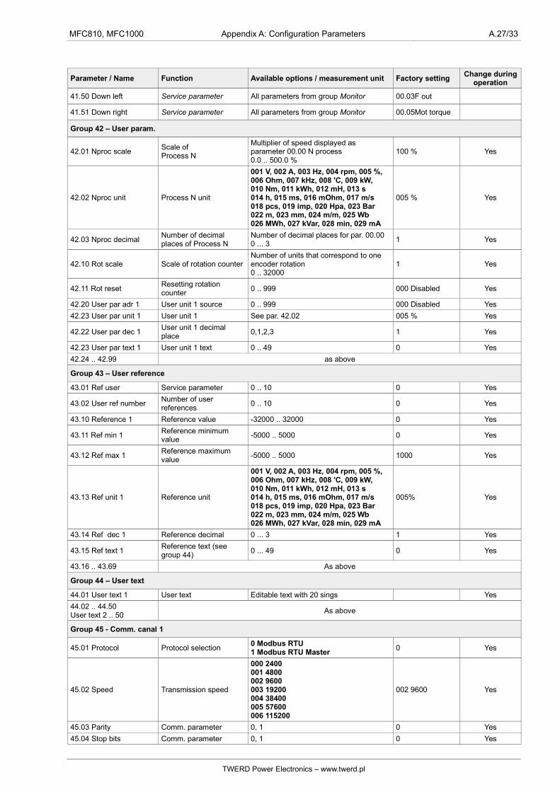
MFC810, MFC1000 Appendix A: Configuration Parameters A.27/33
Parameter / Name Function Available options / measurement unit Factory settingChange during
operation
41.50 Down left Service parameter All parameters from group Monitor 00.03F out
41.51 Down right Service parameter All parameters from group Monitor 00.05Mot torque
Group 42 – User param.
42.01 Nproc scaleScale ofProcess N
Multiplier of speed displayed as parameter 00.00 N process0.0 .. 500.0 %
100 % Yes
42.02 Nproc unit Process N unit
001 V, 002 A, 003 Hz, 004 rpm, 005 %,006 Ohm, 007 kHz, 008 'C, 009 kW,010 Nm, 011 kWh, 012 mH, 013 s014 h, 015 ms, 016 mOhm, 017 m/s018 pcs, 019 imp, 020 Hpa, 023 Bar022 m, 023 mm, 024 m/m, 025 Wb026 MWh, 027 kVar, 028 min, 029 mA
005 % Yes
42.03 Nproc decimalNumber of decimal places of Process N
Number of decimal places for par. 00.00 0 ... 3
1 Yes
42.10 Rot scale Scale of rotation counterNumber of units that correspond to one encoder rotation0 .. 32000
1 Yes
42.11 Rot resetResetting rotation counter
0 .. 999 000 Disabled Yes
42.20 User par adr 1 User unit 1 source 0 .. 999 000 Disabled Yes
42.23 User par unit 1 User unit 1 See par. 42.02 005 % Yes
42.22 User par dec 1User unit 1 decimal place
0,1,2,3 1 Yes
42.23 User par text 1 User unit 1 text 0 .. 49 0 Yes
42.24 .. 42.99 as above
Group 43 – User reference
43.01 Ref user Service parameter 0 .. 10 0 Yes
43.02 User ref numberNumber of user references
0 .. 10 0 Yes
43.10 Reference 1 Reference value -32000 .. 32000 0 Yes
43.11 Ref min 1Reference minimum value
-5000 .. 5000 0 Yes
43.12 Ref max 1Reference maximum value
-5000 .. 5000 1000 Yes
43.13 Ref unit 1 Reference unit
001 V, 002 A, 003 Hz, 004 rpm, 005 %,006 Ohm, 007 kHz, 008 'C, 009 kW,010 Nm, 011 kWh, 012 mH, 013 s014 h, 015 ms, 016 mOhm, 017 m/s018 pcs, 019 imp, 020 Hpa, 023 Bar022 m, 023 mm, 024 m/m, 025 Wb026 MWh, 027 kVar, 028 min, 029 mA
005% Yes
43.14 Ref dec 1 Reference decimal 0 ... 3 1 Yes
43.15 Ref text 1Reference text (see group 44)
0 ... 49 0 Yes
43.16 .. 43.69 As above
Group 44 – User text
44.01 User text 1 User text Editable text with 20 sings Yes
44.02 .. 44.50User text 2 .. 50
As above
Group 45 - Comm. canal 1
45.01 Protocol Protocol selection0 Modbus RTU1 Modbus RTU Master
0 Yes
45.02 Speed Transmission speed
000 2400001 4800002 9600003 19200004 38400005 57600006 115200
002 9600 Yes
45.03 Parity Comm. parameter 0, 1 0 Yes
45.04 Stop bits Comm. parameter 0, 1 0 Yes
TWERD Power Electronics – www.twerd.pl

A.28/33 Appendix A: Configuration Parameters MFC810, MFC1000
Parameter / Name Function Available options / measurement unit Factory settingChange during
operation
45.05 Terminator Comm. parameter 0, 1 0 Yes
45.06 Timeout Comm. parameter 0 .. 600 s 30 s Yes
45.07 Tout reactResponse to lack of communication through RS link
000 None - no response001 Warning - a warning will be displayed, device will keepworking with referenced frequency002 Fault - device will stop and message will be displayed 003 Last freq. - a warning will be displayed, frequency will stay on an average level from last 10s004 Const freq. 15 - device will work withreferenced frequency f const. 15
000 None Yes
Group 46 - Comm. canal 2
46.01 Protocol Protocol selection0 Modbus RTU1 Modbus RTU Master2 CAN
0 Yes
46.02 Speed Transmission speed
000 2400001 4800002 9600003 19200004 38400005 57600006 115200
002 9600 Yes
46.03 Parity Comm. parameter 0, 1 0 Yes
46.04 Stop bits Comm. parameter 0, 1 0 Yes
46.05 Terminator Comm. parameter 0, 1 0 Yes
46.06 Timeout Comm. parameter 0 .. 600 s 30 s Yes
46.07 Tout reactResponse to lack of communication through RS link
000 None - no response001 Warning - a warning will be displayed, device will keepworking with referenced frequency002 Fault - device will stop and message will be displayed 003 Last freq. - a warning will be displayed, frequency will stay on an average level from last 10s004 Const freq. 15 - device will work withreferenced frequency f const. 15
000 None Yes
46.10 CAN ID 1..127 12 Yes1)
46.11 CAN Speed
000 50 kbit001 100kbit002 125 kbit003 250 kbit004 500 kbit005 1000 kbit
004 500 kbit Yes1)
46.12 CAN Profile000 CiA 402011 USER1
000 CiA 402 Yes1)
46.20 Rpdo cobId 1 0 .. 1407 (0x0 .. 0x57F) Yes1)
46.23 Rpdo type 1 0 .. 255 254 Yes1)
46.22 Rpdo event time 1 0 .. 65535 ms 100ms Yes1)
46.25 Tpdo cobId 1 0 .. 1407 (0x0 .. 0x57F) 0 Yes1)
46.26 Tpdo type 1 0 .. 255 254 Yes1)
46.35 Tpdo cobId 5 0 .. 1407 (0x0 .. 0x57F) 0 Yes1)
46.36 Tpdo type 5 0 .. 255 254 Yes1)
46.40 Rpdo cobId 6 0 .. 1407 (0x0 .. 0x57F) 0 Yes1)
46.41 Rpdo type 6 0 .. 255 254 Yes1)
46.42 Rpdo event time 6 0 .. 65535 ms 100ms Yes1)
46.45 Tpdo cobId 6 0 .. 1407 (0x0 .. 0x57F) 0 Yes1)
46.46 Tpdo type 6 0 .. 255 254 Yes1)
46.50 Rpdo cobId 23 0 .. 1407 (0x0 .. 0x57F) 0 Yes1)
46.51 Rpdo type 23 0 .. 255 254 Yes1)
46.52 Rpdo event time 23 0 .. 65535 ms 100ms Yes1)
1) The frequency converter must be restarted
TWERD Power Electronics – www.twerd.pl
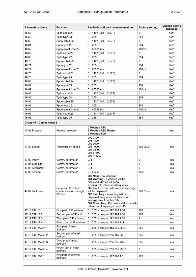
MFC810, MFC1000 Appendix A: Configuration Parameters A.29/33
Parameter / Name Function Available options / measurement unit Factory settingChange during
operation
46.55 Tpdo cobId 23 0 .. 1407 (0x0 .. 0x57F) 0 Yes1)
46.56 Tpdo type 23 0 .. 255 254 Yes1)
46.60 Rpdo cobId 22 0 .. 1407 (0x0 .. 0x57F) 0 Yes1)
46.61 Rpdo type 22 0 .. 255 254 Yes1)
46.62 Rpdo event time 22 0 .. 65535 ms 100ms Yes1)
46.65 Tpdo cobId 22 0 .. 1407 (0x0 .. 0x57F) 0 Yes1)
46.66 Tpdo type 22 0 .. 255 254 Yes1)
46.70 Rpdo cobId 23 0 .. 1407 (0x0 .. 0x57F) 0 Yes1)
46.71 Rpdo type 23 0 .. 255 254 Yes1)
46.72 Rpdo event time 23 0 .. 65535 ms 100ms Yes1)
46.75 Tpdo cobId 23 0 .. 1407 (0x0 .. 0x57F) 0 Yes1)
46.76 Tpdo type 23 0 .. 255 254 Yes1)
46.80 Rpdo cobId 24 0 .. 1407 (0x0 .. 0x57F) 0 Yes1)
46.81 Rpdo type 24 0 .. 255 254 Yes1)
46.82 Rpdo event time 24 0 .. 65535 ms 100ms Yes1)
46.85 Tpdo cobId 24 0 .. 1407 (0x0 .. 0x57F) 0 Yes1)
46.86 Tpdo type 24 0 .. 255 254 Yes1)
46.90 Rpdo cobId 25 0 .. 1407 (0x0 .. 0x57F) 0 Yes1)
46.91 Rpdo type 25 0 .. 255 254 Yes1)
46.92 Rpdo event time 25 0 .. 65535 ms 100ms Yes1)
46.95 Tpdo cobId 25 0 .. 1407 (0x0 .. 0x57F) 0 Yes1)
46.96 Tpdo type 25 0 .. 255 254 Yes1)
Group 47 - Comm. canal 3
47.01 Protocol Protocol selection0 Modbus RTU1 Modbus RTU Master2 Modbus TCP
0 Yes
47.02 Speed Transmission speed
000 2400001 4800002 9600003 19200004 38400005 57600006 115200
002 9600 Yes
47.03 Parity Comm. parameter 0, 1 0 Yes
47.04 Stop bits Comm. parameter 0, 1 0 Yes
47.05 Terminator Comm. parameter 0, 1 0 Yes
47.06 Timeout Comm. parameter 0 .. 600 s 30 s Yes
47.07 Tout reactResponse to lack of communication through RS link
000 None - no response001 Warning - a warning will be displayed, device will keepworking with referenced frequency002 Fault - device will stop and message will be displayed 003 Last freq. - a warning will be displayed, frequency will stay on an average level from last 10s004 Const freq. 15 - device will work withreferenced frequency f const. 15
000 None Yes
47.10 ETH IP 1 First part of IP address 0 .. 255, example: 192.168.1.50 192 Yes
47.11 ETH IP 2 Second part of IP addr. 0 .. 255, example: 192.168.1.50 168 Yes
47.12 ETH IP 3 Third part of IP address 0 .. 255, example: 192.168.1.50 1 Yes
47.13 ETH IP 4 Fourth part of IP address 0 .. 255, example: 192.168.1..2 Yes
47.14 ETH MASK 1First part of mask address
0 .. 255, example: 255.255.255.0 255 Yes
47.15 ETH MASK 2Second part of mask address
0 .. 255, example: 255.255.255.0 255 Yes
47.16 ETH MASK 3Third part of mask address
0 .. 255, example: 255.255.255.0 255 Yes
47.17 ETH MASK 4Fourth part of mask address
0 .. 255, example: 255.255.255.0 0 Yes
47.18 ETH GW 1First part of gateway address
0 .. 255, example: 192.168.1.1 192 Yes
TWERD Power Electronics – www.twerd.pl

A.30/33 Appendix A: Configuration Parameters MFC810, MFC1000
Parameter / Name Function Available options / measurement unit Factory settingChange during
operation
47.19 ETH GW 2Second part of gateway address
0 .. 255, example: 192.168.1.1 168 Yes
47.20 ETH GW 3Third part of gateway address
0 .. 255, example: 192.168.1.1 1 Yes
47.23 ETH GW 4Fourth part of gateway address
0 .. 255, example: 192.168.1.1 1 Yes
47.22 ETH port Ethernet port 0 .. 65535 502 Yes
47.23 ETH dhcp Ethernet DHCP0: No1: Yes
No Yes
47.24 ETH timeout TCP connection timeout 0 .. 600 s 10 s Yes
Group 49 – Parameter mapping
49.00 Fast Read1Selection of the variable assigned to ACTR1
All parameters and PCH PCH770 Yes
49.01 Fast Read2Selection of the variable assigned to ACTR2
All parameters and PCH PCH771 Yes
49.02 Fast Read3Selection of the variable assigned to ACTR3
All parameters and PCH PCH772 Yes
49.03 Fast Read4Selection of the variable assigned to ACTR4
All parameters and PCH PCH773 Yes
49.04 Fast Read5Selection of the variable assigned to ACTR5
All parameters and PCH PCH774 Yes
49.05 Fast Read6Selection of the variable assigned to ACTR6
All parameters and PCH PCH775 Yes
49.06 Fast Read7Selection of the variable assigned to ACTR7
All parameters and PCH PCH776 Yes
49.07 Fast Read8Selection of the variable assigned to ACTR8
All parameters and PCH PCH777 Yes
49.08 Fast Read9Selection of the variable assigned to ACTR9
All parameters and PCH PCH778 Yes
49.09 Fast Read10Selection of the variable assigned to ACTR10
All parameters and PCH PCH779 Yes
49.10 Fast Read11Selection of the variable assigned to ACTR11
All parameters and PCH PCH780 Yes
49.11 Fast Read12Selection of the variable assigned to ACTR12
All parameters and PCH PCH781 Yes
49.12 Fast Read13Selection of the variable assigned to ACTR13
All parameters and PCH PCH782 Yes
49.13 Fast Read14Selection of the variable assigned to ACTR14
All parameters and PCH PCH783 Yes
49.14 Fast Read15Selection of the variable assigned to ACTR15
All parameters and PCH PCH784 Yes
49.15 Fast Read16Selection of the variable assigned to ACTR16
All parameters and PCH PCH785 Yes
49.16 Fast Read17Selection of the variable assigned to ACTR17
All parameters and PCH PCH786 Yes
49.15 Fast Read18Selection of the variable assigned to ACTR18
All parameters and PCH PCH787 Yes
49.18 Fast Read19Selection of the variable assigned to ACTR19
All parameters and PCH PCH788 Yes
49.19 Fast Read20Selection of the variable assigned to ACTR20
All parameters and PCH PCH789 Yes
49.20 Fast write1Selection of the variable assigned to ACTW01
All parameters and PCH PCH750 Yes
49.23 Fast write2Selection of the variable assigned to ACTW02
All parameters and PCH PCH751 Yes
49.22 Fast write3Selection of the variable assigned to ACTW03
All parameters and PCH PCH752 Yes
49.23 Fast write4Selection of the variable assigned to ACTW04
All parameters and PCH PCH753 Yes
49.24 Fast write5Selection of the variable assigned to ACTW05
All parameters and PCH PCH754 Yes
49.25 Fast write6Selection of the variable assigned to ACTW06
All parameters and PCH PCH755 Yes
TWERD Power Electronics – www.twerd.pl
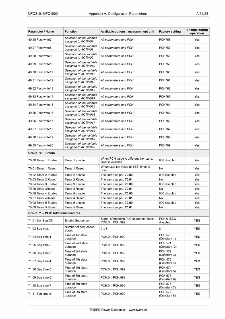
MFC810, MFC1000 Appendix A: Configuration Parameters A.31/33
Parameter / Name Function Available options / measurement unit Factory settingChange during
operation
49.26 Fast write7Selection of the variable assigned to ACTW07
All parameters and PCH PCH756 Yes
49.27 Fast write8Selection of the variable assigned to ACTW08
All parameters and PCH PCH757 Yes
49.28 Fast write9Selection of the variable assigned to ACTW09
All parameters and PCH PCH758 Yes
49.29 Fast write10Selection of the variable assigned to ACTW010
All parameters and PCH PCH759 Yes
49.30 Fast write11Selection of the variable assigned to ACTW011
All parameters and PCH PCH760 Yes
49.31 Fast write12Selection of the variable assigned to ACTW012
All parameters and PCH PCH761 Yes
49.32 Fast write13Selection of the variable assigned to ACTW013
All parameters and PCH PCH762 Yes
49.33 Fast write14Selection of the variable assigned to ACTW014
All parameters and PCH PCH763 Yes
49.34 Fast write15Selection of the variable assigned to ACTW015
All parameters and PCH PCH764 Yes
49.35 Fast write16Selection of the variable assigned to ACTW016
All parameters and PCH PCH765 Yes
49.36 Fast write17Selection of the variable assigned to ACTW017
All parameters and PCH PCH766 Yes
49.37 Fast write18Selection of the variable assigned to ACTW018
All parameters and PCH PCH767 Yes
49.38 Fast write19Selection of the variable assigned to ACTW019
All parameters and PCH PCH768 Yes
49.39 Fast write20Selection of the variable assigned to ACTW020
All parameters and PCH PCH769 Yes
Group 70 – Timers
70.00 Timer 1 Enable Timer 1 enableWhen PCH value is different then zero, timer is enabled
000 disabled Yes
70.01 Timer 1 Reset Timer 1 ResetWhen user set value to YES, timer is reset.
No Yes
70.02 Timer 2 Enable Timer 2 enable The same as par. 70.00 000 disabled Yes
70.03 Timer 2 Reset Timer 2 Reset The same as par. 70.01 No Yes
70.04 Timer 3 Enable Timer 3 enable The same as par. 70.00 000 disabled Yes
70.05 Timer 3Reset Timer 3 Reset The same as par. 70.01 No Yes
70.06 Timer 4 Enable Timer 4 enable The same as par. 70.00 000 disabled Yes
70.07 Timer 4Reset Timer 4 Reset The same as par. 70.01 No Yes
70.08 Timer 5 Enable Timer 5 enable The same as par. 70.00 000 disabled Yes
70.09 Timer 5 Reset Timer 5 Reset The same as par. 70.01 No Yes
Group 71 – PLC: Additional features
71.01 Sw. Seq ON Enable SequencerSignal of enabling PLC sequencer blockPCH.0 .. PCH.999
PCH.0 (SEQ disabled)
YES
71.03 Seq maxNumber of sequencer states
2 .. 8 8 YES
71.04 Seq time 1Time of 1st state duration
PCH.0 .. PCH.999PCH.570 (Constant 1)
YES
71.05 Seq time 2Time of 2nd state duration
PCH.0 .. PCH.999PCH.571 (Constant 2)
YES
71.06 Seq time 3Time of 3rd state duration
PCH.0 .. PCH.999PCH.572 (Constant 3)
YES
71.07 Seq time 4Time of 4th state duration
PCH.0 .. PCH.999PCH.573 (Constant 4)
YES
71.08 Seq time 5Time of 5th state duration
PCH.0 .. PCH.999PCH.574 (Constant 5)
YES
71.09 Seq time 6Time of 6th state duration
PCH.0 .. PCH.999PCH.575 (Constant 6)
YES
71.10 Seq time 7Time of 7th state duration
PCH.0 .. PCH.999PCH.576 (Constant 7)
YES
71.11 Seq time 8Time of 8th state duration
PCH.0 .. PCH.999PCH.577 (Constant 8)
YES
TWERD Power Electronics – www.twerd.pl
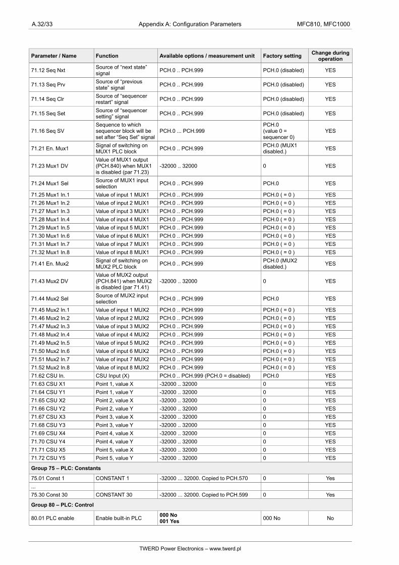
A.32/33 Appendix A: Configuration Parameters MFC810, MFC1000
Parameter / Name Function Available options / measurement unit Factory settingChange during
operation
71.12 Seq NxtSource of “next state” signal
PCH.0 .. PCH.999 PCH.0 (disabled) YES
71.13 Seq PrvSource of “previous state” signal
PCH.0 .. PCH.999 PCH.0 (disabled) YES
71.14 Seq ClrSource of “sequencer restart” signal
PCH.0 .. PCH.999 PCH.0 (disabled) YES
71.15 Seq SetSource of “sequencer setting” signal
PCH.0 .. PCH.999 PCH.0 (disabled) YES
71.16 Seq SVSequence to which sequencer block will be set after “Seq Set” signal
PCH.0 ... PCH.999PCH.0(value 0 = sequencer 0)
YES
71.21 En. Mux1Signal of switching on MUX1 PLC block
PCH.0 .. PCH.999PCH.0 (MUX1 disabled.)
YES
71.23 Mux1 DVValue of MUX1 output (PCH.840) when MUX1 is disabled (par 71.23)
-32000 .. 32000 0 YES
71.24 Mux1 SelSource of MUX1 input selection
PCH.0 .. PCH.999 PCH.0 YES
71.25 Mux1 In.1 Value of input 1 MUX1 PCH.0 .. PCH.999 PCH.0 ( = 0 ) YES
71.26 Mux1 In.2 Value of input 2 MUX1 PCH.0 .. PCH.999 PCH.0 ( = 0 ) YES
71.27 Mux1 In.3 Value of input 3 MUX1 PCH.0 .. PCH.999 PCH.0 ( = 0 ) YES
71.28 Mux1 In.4 Value of input 4 MUX1 PCH.0 .. PCH.999 PCH.0 ( = 0 ) YES
71.29 Mux1 In.5 Value of input 5 MUX1 PCH.0 .. PCH.999 PCH.0 ( = 0 ) YES
71.30 Mux1 In.6 Value of input 6 MUX1 PCH.0 .. PCH.999 PCH.0 ( = 0 ) YES
71.31 Mux1 In.7 Value of input 7 MUX1 PCH.0 .. PCH.999 PCH.0 ( = 0 ) YES
71.32 Mux1 In.8 Value of input 8 MUX1 PCH.0 .. PCH.999 PCH.0 ( = 0 ) YES
71.41 En. Mux2Signal of switching on MUX2 PLC block
PCH.0 .. PCH.999PCH.0 (MUX2 disabled.)
YES
71.43 Mux2 DVValue of MUX2 output (PCH.841) when MUX2 is disabled (par 71.41)
-32000 .. 32000 0 YES
71.44 Mux2 SelSource of MUX2 input selection
PCH.0 .. PCH.999 PCH.0 YES
71.45 Mux2 In.1 Value of input 1 MUX2 PCH.0 .. PCH.999 PCH.0 ( = 0 ) YES
71.46 Mux2 In.2 Value of input 2 MUX2 PCH.0 .. PCH.999 PCH.0 ( = 0 ) YES
71.47 Mux2 In.3 Value of input 3 MUX2 PCH.0 .. PCH.999 PCH.0 ( = 0 ) YES
71.48 Mux2 In.4 Value of input 4 MUX2 PCH.0 .. PCH.999 PCH.0 ( = 0 ) YES
71.49 Mux2 In.5 Value of input 5 MUX2 PCH.0 .. PCH.999 PCH.0 ( = 0 ) YES
71.50 Mux2 In.6 Value of input 6 MUX2 PCH.0 .. PCH.999 PCH.0 ( = 0 ) YES
71.51 Mux2 In.7 Value of input 7 MUX2 PCH.0 .. PCH.999 PCH.0 ( = 0 ) YES
71.52 Mux2 In.8 Value of input 8 MUX2 PCH.0 .. PCH.999 PCH.0 ( = 0 ) YES
71.62 CSU In. CSU Input (X) PCH.0 .. PCH.999 (PCH.0 = disabled) PCH.0 YES
71.63 CSU X1 Point 1, value X -32000 .. 32000 0 YES
71.64 CSU Y1 Point 1, value Y -32000 .. 32000 0 YES
71.65 CSU X2 Point 2, value X -32000 .. 32000 0 YES
71.66 CSU Y2 Point 2, value Y -32000 .. 32000 0 YES
71.67 CSU X3 Point 3, value X -32000 .. 32000 0 YES
71.68 CSU Y3 Point 3, value Y -32000 .. 32000 0 YES
71.69 CSU X4 Point 4, value X -32000 .. 32000 0 YES
71.70 CSU Y4 Point 4, value Y -32000 .. 32000 0 YES
71.71 CSU X5 Point 5, value X -32000 .. 32000 0 YES
71.72 CSU Y5 Point 5, value Y -32000 .. 32000 0 YES
Group 75 – PLC: Constants
75.01 Const 1 CONSTANT 1 -32000 ... 32000. Copied to PCH.570 0 Yes
...
75.30 Const 30 CONSTANT 30 -32000 ... 32000. Copied to PCH.599 0 Yes
Group 80 – PLC: Control
80.01 PLC enable Enable built-in PLC000 No001 Yes
000 No No
TWERD Power Electronics – www.twerd.pl
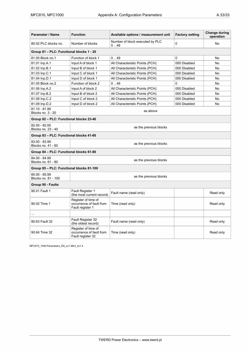
MFC810, MFC1000 Appendix A: Configuration Parameters A.33/33
Parameter / Name Function Available options / measurement unit Factory settingChange during
operation
80.02 PLC blocks no. Number of blocksNumber of block executed by PLC0 .. 48
0 No
Group 81 – PLC: Functional blocks 1 - 20
81.00 Block no.1 Function of block 1 0 .. 49 0 No
81.01 Inp.A.1 Input A of block 1 All Characteristic Points (PCH) 000 Disabled No
81.02 Inp.B.1 Input B of block 1 All Characteristic Points (PCH) 000 Disabled No
81.03 Inp.C.1 Input C of block 1 All Characteristic Points (PCH) 000 Disabled No
81.04 Inp.D.1 Input D of block 1 All Characteristic Points (PCH) 000 Disabled No
81.05 Block no.2 Function of block 2 0 .. 49 0 No
81.06 Inp.A.2 Input A of block 2 All Characteristic Points (PCH) 000 Disabled No
81.07 Inp.B.2 Input B of block 2 All Characteristic Points (PCH) 000 Disabled No
81.08 Inp.C.2 Input C of block 2 All Characteristic Points (PCH) 000 Disabled No
81.09 Inp.D.2 Input D of block 2 All Characteristic Points (PCH) 000 Disabled No
81.10 - 81.99 Blocks no. 3 - 20
as above
Group 82 – PLC: Functional blocks 23-40
82.00 - 82.00Blocks no. 23 - 40
as the previous blocks
Group 83 – PLC: Functional blocks 41-60
83.00 - 83.99Blocks no. 41 - 60
as the previous blocks
Group 84 – PLC: Functional blocks 61-80
84.00 - 84.99Blocks no. 61 - 80
as the previous blocks
Group 85 – PLC: Functional blocks 81-100
85.00 - 85.99Blocks no. 81 - 100
as the previous blocks
Group 90 - Faults
90.01 Fault 1 Fault Register 1(the most current record)
Fault name (read only) Read only
90.02 Time 1Register of time of occurrence of fault from Fault register 1
Time (read only) Read only
...
90.63 Fault 32Fault Register 32(the oldest record)
Fault name (read only) Read only
90.64 Time 32Register of time of occurrence of fault from Fault register 32
Time (read only) Read only
MFC810_1000-Parameters_EN_sv1.98r3_dv1.4
TWERD Power Electronics – www.twerd.pl

MFC810, MFC1000 Appendix B: Failures and warnings codes B.1/9
Appendix B: Failures and warnings codes
Software version: 1.98 rev. 3Document version: 1.1
Failure/warningcode(CANopen)
Displayedname
Description Possible reason Counteraction Status
100...200: control circuits errors
101(6200h)
Program error 1 Program error: ST
Corrupted program memory, external electromagnetic disturbance
Turn the power off and on again. Contact service
Failure
102(6200h)
Program error 2Program error: VSD
Failure
103(6200h)
Program error 3Program error: AcR
Warning
110(6310h)
EEPROM CRC error
Parameters memory error
Corrupted parameter memory, external electromagnetic disturbance
Turn the power off and on again. Upload factory parameters.Contact service
WarningFailure
111(6200h)
No VSD dataMissing data from VSD module
Missing/wrong connection between control board andVSD board
Turn the power off and on again. Check connection between boards. Contact service.
Failure
112(6200h)
No ACR dataMissing data from ACR module
Missing/wrong connection between control board andACR board
Turn the power off and on again. Check connection between boards. Contact service
Failure
120(7500h) No keypad
Failure of the communication with Control panel
Damage of the control panel or connecting cable.
Check connections: wires, plugs
WarningFailure
121(7500h)
Comm. err. VSDLack of communication with VSD module
Failure of the VSD moduleor internal connection cable
Contact service
Failure
122(7500h)
Comm. err. ACRLack of communication with AcR module
Failure of the AcR module or internal connection cable
Warning
123(7500h)
Comm. error „1” Communication canal 1 failure
Failure of a cable, parameters of the transmission are incorrectly set up
Check external connectionsand validity of communication canals parameters
WarningFailure
124(7500h)
Comm. error „2”Communication canal 2 failure
Failure of a cable, parameters of the transmission are incorrectly set up
Check external connectionsand validity of communication canals parameters
WarningFailure
125 Comm. error „3”Communication canal 3 failure
Failure of a cable, parameters of the transmission are incorrectly set up
Check external connectionsand validity of communication canals parameters
WarningFailure
TWERD Power Electronics – www.twerd.pl
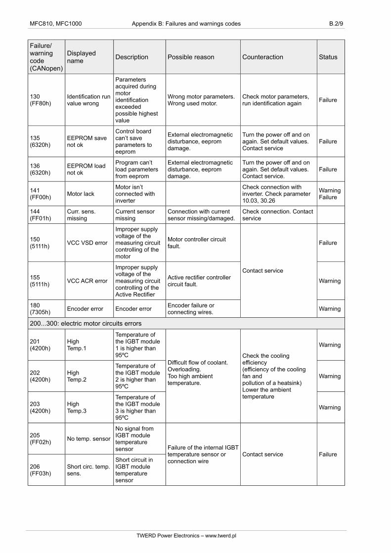
MFC810, MFC1000 Appendix B: Failures and warnings codes B.2/9
Failure/warningcode(CANopen)
Displayedname
Description Possible reason Counteraction Status
130(FF80h)
Identification runvalue wrong
Parameters acquired during motor identification exceeded possible highest value
Wrong motor parameters. Wrong used motor.
Check motor parameters, run identification again
Failure
135(6320h)
EEPROM save not ok
Control board can’t save parameters to eeprom
External electromagnetic disturbance, eeprom damage.
Turn the power off and on again. Set default values. Contact service
Failure
136(6320h)
EEPROM load not ok
Program can’t load parameters from eeprom
External electromagnetic disturbance, eeprom damage.
Turn the power off and on again. Set default values. Contact service.
Failure
141(FF00h)
Motor lackMotor isn’t connected with inverter
Check connection with inverter. Check parameter 10.03, 30.26
WarningFailure
144(FF01h)
Curr. sens. missing
Current sensor missing
Connection with current sensor missing/damaged.
Check connection. Contact service
150(5111h)
VCC VSD error
Improper supply voltage of the measuring circuit controlling of the motor
Motor controller circuit fault.
Contact service
Failure
155(5111h)
VCC ACR error
Improper supply voltage of the measuring circuit controlling of the Active Rectifier
Active rectifier controller circuit fault.
Warning
180(7305h)
Encoder error Encoder errorEncoder failure or connecting wires.
Warning
200...300: electric motor circuits errors
201(4200h)
HighTemp.1
Temperature of the IGBT module 1 is higher than 95ºC
Difficult flow of coolant.Overloading.Too high ambient temperature.
Check the cooling efficiency(efficiency of the cooling fan andpollution of a heatsink)Lower the ambient temperature
Warning
202(4200h)
HighTemp.2
Temperature of the IGBT module 2 is higher than 95ºC
Warning
203(4200h)
HighTemp.3
Temperature of the IGBT module 3 is higher than 95ºC
Warning
205(FF02h)
No temp. sensor
No signal from IGBT module temperature sensor Failure of the internal IGBT
temperature sensor or connection wire
Contact service Failure
206(FF03h)
Short circ. temp.sens.
Short circuit in IGBT module temperature sensor
TWERD Power Electronics – www.twerd.pl

MFC810, MFC1000 Appendix B: Failures and warnings codes B.3/9
Failure/warningcode(CANopen)
Displayedname
Description Possible reason Counteraction Status
211(4200h)
Too high Temp.1
Temperature of the IGBT module 1 is higher than 100ºC
Hindered flow of air of FC.Overloading.Too high ambient temperature.
Check the cooling efficiency(efficiency of the cooling fan andpollution of a heatsink)Lower the ambient temperature
Failure212(4200h)
Too high Temp.2
Temperature of the IGBT module 2 is higher than 100ºC
213(4200h)
Too high Temp.3
Temperature of the IGBT module 3 is higher than 100ºC
217(7520h)
VSD comm. error 2
Communication failure of the VSD module
Failure of the VSD moduleor connection wire
Contact service Failure
220(3211h)
High UDC hardware
High voltage in DC circuit - hardware notification
Too high voltage in the circuit.Too intensive braking of the electric motor
Check the supply voltage.Increase a time of deceleration in(par. 13.02 or 13.11.Deactivate the parameter 13.20 (setting 0.0) or increase its value.
Failure
221(3212h)
High UDCsoftware 1
High voltage in DC circuit - software notification
Failure
222(3212h)
High UDCsoftware 2
High voltage in DC circuit - software notification
Failure
223(3212h)
High UDCsoftware 3
High voltage in DC circuit - software notification
Failure
230(4310h)
High temp. Motor
Electric motor temperature reached I or II threshold
Hindered flow of air of an electric motor.Too high ambient temperature.Working on an overloaded engine or long operating time at heavy load andlow speed.
Check loading of the motor - currentof the motor.Additional cooling fan may be required at low speeds of the electric motor
Warning
231(4310h)
Too high motor temp.
Electric motor temperature reached III threshold
Failure
240(2300h)
High current 1
The output currentof the FC is to high - hardware notification
Too high intensity of acceleration of an electric motor.A sudden change of electric motor loading.
Increase an acceleration time of the electric motor. Failure
241(2300h)
High current 2
The output currentof the FC is to high - software notification
244(2311h)
Inverter overloadThermal i2t overload of the converter
The inverter is overloaded - output current is to high (Iout>1.5In@60sec)
Reduce the inverter load. Failure
245(2300h)
High current motor
Overload of the electric motor
Electric motor is overloaded - to high current.
Reduce the electric motor load
Failure
TWERD Power Electronics – www.twerd.pl

MFC810, MFC1000 Appendix B: Failures and warnings codes B.4/9
Failure/warningcode(CANopen)
Displayedname
Description Possible reason Counteraction Status
248(2330h)
Earthing
The sum of el. motor currents isnot equal to null
Defective insulation of windings of the el. motoror connecting wires
Check isolation resistance of thewires connecting the el. motor and theconverter and isolation resistance ofwindings of the el. motor.
Failure
250(2320h)
VSD IGBT driverfault
Short circuit on output of theconverter or failure of VSD IGBT module
Short circuit in the el. motor or in thewires feeding the el. motor.
Disconnect the el. motor and testpresence of a short circuit, if presentcall service to repair FC, and if isnot present test isolation of wires andwindings of the el. motor
Failure
251VSD IGBT supply
Failure
252VSD IGBT 1", "driver fault"
Short circuit on output of theconverter or failure of VSD IGBT module
Short circuit in the el. motor or in thewires feeding the el. motor.
Disconnect the el. motor and testpresence of a short circuit, if presentcall service to repair FC, and if isnot present test isolation of wires andwindings of the el. motor
Failure
253"VSD IGBT 1", "supply"
Failure
254"VSD IGBT 2", "driver fault"
Short circuit on output of theconverter or failure of VSD IGBT module
Short circuit in the el. motor or in thewires feeding the el. motor.
Disconnect the el. motor and testpresence of a short circuit, if presentcall service to repair FC, and if isnot present test isolation of wires andwindings of the el. motor
Failure
255VSD IGBT 2", "supply"
Failure
256VSD IGBT U", "driver fault"
Short circuit on output of theconverter or failure of VSD IGBT module
Short circuit in the el. motor or in thewires feeding the el. motor.
Disconnect the el. motor and testpresence of a short circuit, if presentcall service to repair FC, and if isnot present test isolation of wires andwindings of the el. motor
Failure
257"VSD IGBT V", "driver fault"
Short circuit on output of theconverter or failure of VSD IGBT module
Short circuit in the el. motor or in thewires feeding the el. motor.
Disconnect the el. motor and testpresence of a short circuit, if presentcall service to repair FC, and if isnot present test isolation of wires andwindings of the el. motor
Failure
TWERD Power Electronics – www.twerd.pl

MFC810, MFC1000 Appendix B: Failures and warnings codes B.5/9
Failure/warningcode(CANopen)
Displayedname
Description Possible reason Counteraction Status
258"VSD IGBT W", "driver fault"
Short circuit on output of theconverter or failure of VSD IGBT module
Short circuit in the el. motor or in thewires feeding the el. motor.
Disconnect the el. motor and testpresence of a short circuit, if presentcall service to repair FC, and if isnot present test isolation of wires andwindings of the el. motor
Failure
259"VSD IGBT BR","driver fault"
Short circuit on output of theconverter or failure of VSD IGBT module
Short circuit in the el. motor or in thewires feeding the el. motor.
Disconnect the el. motor and testpresence of a short circuit, if presentcall service to repair FC, and if isnot present test isolation of wires andwindings of the el. motor
Failure
260(FF04h)
Output asymmetry
Asymmetrical loading
The el. motor failure or absence ofoutput phase (damage of awire)
Check connections of theFC - el. motor, check resistance ofel. motor windings, replace the el. motor.
Warning
265(3230h)
Underload
Operation with loading whichis much lower than nominal
Parameters of a underloadareincorrectly determined
Check and correct parameter settingswhich refer to underload of theconverter
Warning
268(7121h)
Stall
The el. motor has stopped underact of too high loading.
Too high anti-torque, failure of theoperating device, to low power ofthe converter
Check operating device (jam).Increase boost U0 voltage (par. 15.01) of the frequency converter - only in scalar mode.Reduce the load on the electric motor
Failure
270(FF05h)
F>MAX
Output frequency of thefrequency converter is higherthan the maximum frequency
Operation device rolls the motor upor there is a big readjustment ofthe speed regulator
Modify the speed regulator settings
Failure
275(FF06h)
Speed control
Error of output speed -difference between referenceand output speed exceedacceptable difference (par.30.61) or time (par. 30.62).
Incorrect setting the dynamics ofthe drive; output values offrequency converter reachedoperational limits of: current, torqueand/or voltage
Check the drive system, the driveload. Change the parameters settings 30.60, 30.61, 30.62
Warning
TWERD Power Electronics – www.twerd.pl

MFC810, MFC1000 Appendix B: Failures and warnings codes B.6/9
Failure/warningcode(CANopen)
Displayedname
Description Possible reason Counteraction Status
277(2310h)
I2T motor 1
Overheating of the el. motor 1
Overheating of the motor or operation with high loading at smallspeeds
Check loading of the motor (currentof the motor); check parameters ofthermal el. motor model
Failure
278(2310h)
I2T motor 2
Overheating of the el. motor 2
Overheating of the motor or operation with high loading at smallspeeds
Check loading of the el. motor (currentof the el. motor); check parameters ofthermal el. motor model
Failure
280
(FF0Ah)
Ext. block VSD
Internal failure - Contact service -
285
(FF07h)
Motor param. error
Wrong motor parameters
Parameters 10.01÷ 10.06 defined in group 10 are incorrect.
Check motor parameters entered in group 10.
Failure
290(FF08h)
Current testInverter current test
Current time exceeded value from parameter 38.02
Failure
291 VSD fan failure Failure
295
(7112h)
Chopper Overload
Chopper temperature overloaded
Improper brake resistor.Improper brake resistor parameters.
Choose the right braking resistors.Check parameters 34.01 - 34.04
WarningFailure
296
(7111h) Chopper ErrorChopper IGBT driver failure
Contact service Failure
300...400: line circuits errors
301(4200h)
HighTemp.ACR1
Temperature of the IGBT module 1 is higher than 100ºC
Difficult flow of coolant.Overloading.Too high ambient temperature.
Check the cooling efficiency(efficiency of the cooling fan andpollution of a heatsink)Lower the ambient temperature
Warning302(4200h)
HighTemp.ACR2
Temperature of the IGBT module 2 is higher than 100ºC
303(4200h)
HighTemp.ACR3
Temperature of the IGBT module 3 is higher than 100ºC
305(FF42h)
No temp. sensor
No signal from IGBT module temperature sensor Failure of the internal IGBT
temperature sensor or connection wire
Contact service Warning
306(FF43h)
Short cric. temp.sens.
Short circuit in IGBT module temperature sensor
311(4200h)
Too hightemp. ACR1
Temperature of the IGBT module 1 is higher than 110ºC
Difficult flow of coolant.Overloading.Too high ambient temperature.
Check the cooling efficiency(efficiency of the cooling fan and
Warning+Stop AcR
TWERD Power Electronics – www.twerd.pl

MFC810, MFC1000 Appendix B: Failures and warnings codes B.7/9
Failure/warningcode(CANopen)
Displayedname
Description Possible reason Counteraction Status
pollution of a heatsink)Lower the ambient temperature
312(4200h)
Too hightemp. ACR2
Temperature of the AcR IGBT module 1 is higherthan 110ºC
313(4200h)
Too hightemp. ACR3
Temperature of the AcR IGBT module 1 is higherthan 110ºC
317(7520h)
ACR comm. error 2
Communication failure of the VSD module
Failure of the VSD moduleor connection wire
Contact service Warning
320(3221h)
Low DCLow voltage in DCcircuit
Low supply voltage, absence ofone phase of a supply voltage.
Check a connecting cables and a supply voltage on a mains terminals
Warning+Stop AcR
321(3130h)
Phase missingNo one phase in the supply voltage
Absence ofone phase of a supply voltage.Disconnected or damaged power supply cable.
325(FF44h)
Load circ. error 1
Pre-charging circuit isn’t switched on
Failure in pre-charging circuit.
Check the pre-charge circuit.
Failure
326(FF45h)
Load circ. error 2
Too long pre-charging time
Failure
330(3211h)
High UDC hardware
High voltage in DC circuit - hardware notification
Too high voltage in the circuit.Too intensive braking of the electric motor
Check grid voltage.Increase breaking time (delay) par 13.02 or 13.11
Failure
331(3212h)
High UDC software
High voltage in DC circuit - software notification
Failure
332High UDC hardware
High voltage in half DC circuit (3lvl inverter)
Contact service. Failure
333High UDC hardware
Too much difference between capacitors (3lvl inverter)
Contact service. Failure
340(2100h)
High curr. grid
The input current of the FC is to high - hardware notification
Too high intensity of acceleration of an electric motorA sudden change of electric motor loading.
Increase an acceleration time of the electric motor
Warning+Stop AcR
341(2100h)
High curr. grid
The input current of the FC is to high - software notification
Warning+Stop AcR
TWERD Power Electronics – www.twerd.pl
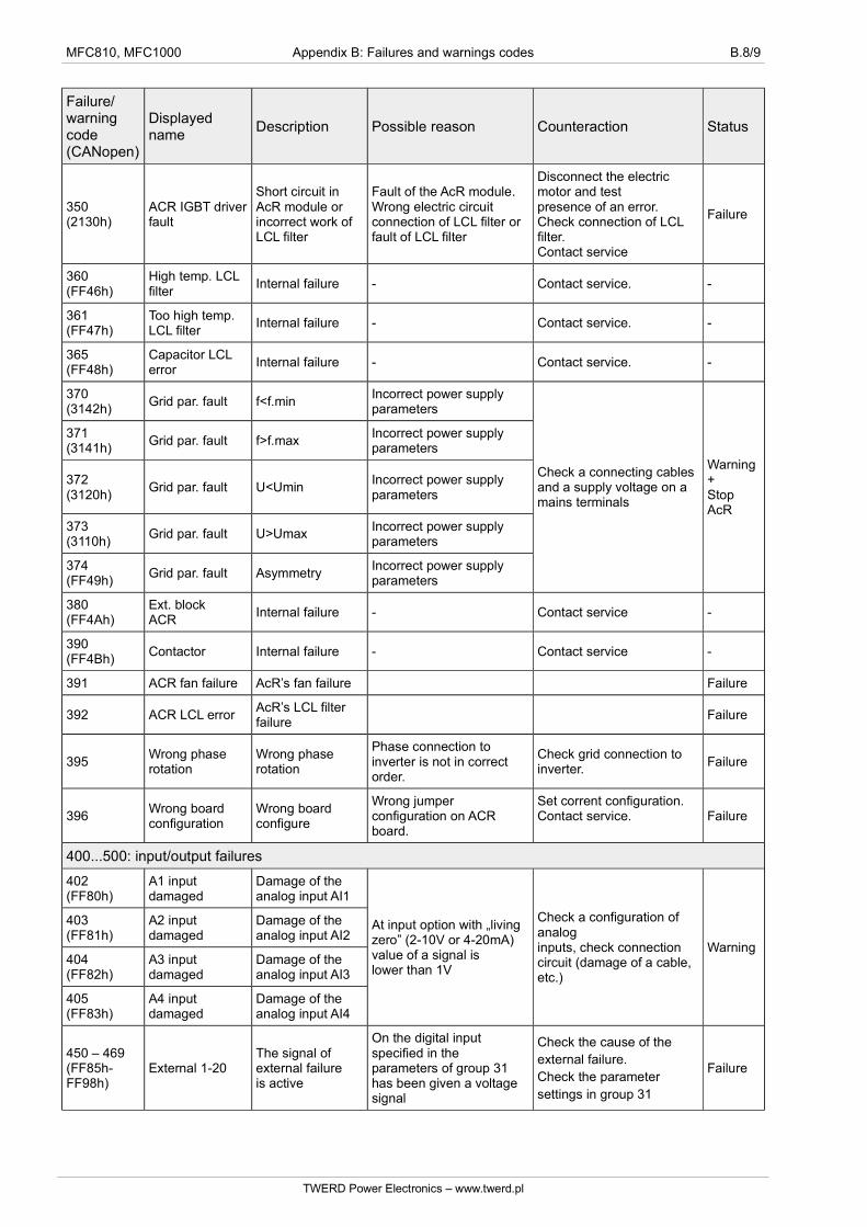
MFC810, MFC1000 Appendix B: Failures and warnings codes B.8/9
Failure/warningcode(CANopen)
Displayedname
Description Possible reason Counteraction Status
350(2130h)
ACR IGBT driverfault
Short circuit in AcR module or incorrect work of LCL filter
Fault of the AcR module.Wrong electric circuit connection of LCL filter or fault of LCL filter
Disconnect the electric motor and testpresence of an error.Check connection of LCL filter.Contact service
Failure
360(FF46h)
High temp. LCL filter
Internal failure - Contact service. -
361(FF47h)
Too high temp. LCL filter
Internal failure - Contact service. -
365(FF48h)
Capacitor LCL error
Internal failure - Contact service. -
370(3142h)
Grid par. fault f<f.minIncorrect power supply parameters
Check a connecting cables and a supply voltage on a mains terminals
Warning+Stop AcR
371(3141h)
Grid par. fault f>f.maxIncorrect power supply parameters
372(3120h)
Grid par. fault U<UminIncorrect power supply parameters
373(3110h)
Grid par. fault U>UmaxIncorrect power supply parameters
374(FF49h)
Grid par. fault AsymmetryIncorrect power supply parameters
380(FF4Ah)
Ext. blockACR
Internal failure - Contact service -
390(FF4Bh)
Contactor Internal failure - Contact service -
391 ACR fan failure AcR’s fan failure Failure
392 ACR LCL errorAcR’s LCL filter failure
Failure
395Wrong phaserotation
Wrong phaserotation
Phase connection to inverter is not in correct order.
Check grid connection to inverter.
Failure
396Wrong board configuration
Wrong board configure
Wrong jumper configuration on ACR board.
Set corrent configuration.Contact service. Failure
400...500: input/output failures
402(FF80h)
A1 input damaged
Damage of the analog input AI1
At input option with „living zero” (2-10V or 4-20mA) value of a signal islower than 1V
Check a configuration of analoginputs, check connection circuit (damage of a cable, etc.)
Warning
403(FF81h)
A2 input damaged
Damage of the analog input AI2
404(FF82h)
A3 input damaged
Damage of the analog input AI3
405(FF83h)
A4 input damaged
Damage of the analog input AI4
450 – 469(FF85h-FF98h)
External 1-20The signal of external failureis active
On the digital input specified in the parameters of group 31 has been given a voltage signal
Check the cause of the
external failure.
Check the parameter
settings in group 31
Failure
TWERD Power Electronics – www.twerd.pl

MFC810, MFC1000 Appendix B: Failures and warnings codes B.9/9
Failure/warningcode(CANopen)
Displayedname
Description Possible reason Counteraction Status
470No temp. cab. sensor
Lack of cabinet’s temperature sensor
Sensor is damaged or unconnected
Check if the sensor is
working correctly. Check
the sensor’s wiring.
Warning
471High temp. cabinet
The temperature inside cabinet is too high
Cabinet fans failure or hindered flow of air
Check fans, check the
cabinet air filter clogging.Warning
480(FF84h)
Emergency stopActive emergencystop
The emergency stop has been activated
Check and remove the
cause of emergency stop
activation.
Check parameter 26.03
Failure
490(4220h)
Too low temperature
Temperature of the heatsink is lower than -100C
Temperature of converter’senvironment it too low
Check efficiency of heating Failure
MF810_1000-Faults_EN_sv1.98r3_dv1.1.odt
TWERD Power Electronics – www.twerd.pl

MFC810, MFC1000 Appendix C: Characteristic Points PCH C.1/11
Appendix C: Characteristic Points PCH
Software version: 1.98 rev. 3Document version: 1.1
PCH PCH name Function / value / note
000 DISABLED Value always = L (logical 0)
001 Input 1 State of digital input 1; L = 0V, H = 24V
002 Input 2 State of digital input 2; L = 0V, H = 24V
003 Input 3 State of digital input 3; L = 0V, H = 24V
004 Input 4 State of digital input 4; L = 0V, H = 24V
005 Input 5 State of digital input 5; L = 0V, H = 24V
006 Input 6 State of digital input 6; L = 0V, H = 24V
007 Input 7 State of digital input 7; L = 0V, H = 24V
008 Input 8 State of digital input 8; L = 0V, H = 24V
009 Input 9 State of digital input 9; L = 0V, H = 24V
010 Input 10 State of digital input 10; L = 0V, H = 24V
011..018 Input 11 .. Input 18 State of additional digital inputs 11..18 on SLOT 0; L = 0V, H = 24V
021..026 Input 21 .. Input 26 State of additional digital inputs 21..26 on SLOT 1; L = 0V, H = 24V
031..036 Input 31 .. Input 36 State of additional digital inputs 31..36 on SLOT 2; L = 0V, H = 24V
041..046 Input 41 .. Input 46 State of additional digital inputs 41..46 on SLOT 3; L = 0V, H = 24V
051..056 Input 51 .. Input 56 State of additional digital inputs 51..56 on SLOT 4; L = 0V, H = 24V
061..068 Output 1 .. Output 8 State of relay outputs K1..K8. H = it is switched ON
071..076 Output 11 .. Output 16
State of additional relay outputs K11..K16 on SLOT 0. H = it is switched ON
081..086 Output 21 .. Output 26
State of additional relay outputs K21..K26 on SLOT 1. H = it is switched ON
091..096 Output 31 .. Output 36
State of additional relay outputs K31..K36 on SLOT 2. H = it is switched ON
101..106 Output 41 .. Output 46
State of additional relay outputs K41..K46 on SLOT 3. H = it is switched ON
111..116 Output 51 .. Output 56
State of additional relay outputs K51..K56 on SLOT 4. H = it is switched ON
120 An. inp 0 Value corresponding to voltage of analog input 0.Resolution 0.1 %, range 0..1000 = 0.0..100.0 %.
121 An. inp 1 Value corresponding to voltage or current of analog input 1.Resolution 0.1 %, range 0..1000 = 0.0..100.0 %.
122 An. inp 2 Value corresponding to voltage or current of analog input 2.Resolution 0.1 %, range 0..1000 = 0.0..100.0 %.
123 An. inp 3 Value corresponding to voltage or current of analog input 3.Resolution 0.1 %, range 0..1000 = 0.0..100.0 %.
124 An. inp 4 Value corresponding to voltage or current of analog input 4.Resolution 0.1 %, range 0..1000 = 0.0..100.0 %.
130 An. inp 11 Value corresponding to voltage of additional analog input 11 on SLOT 0Resolution 0.1 %, range 0..1000 = 0.0..100.0 %.
TWERD Power Electronics - www.twerd.pl

MFC810, MFC1000 Appendix C: Characteristic Points PCH C.2/11
PCH PCH name Function / value / note
131 An. inp 12 Value corresponding to voltage or current of additional analog input 12 on SLOT 0Resolution 0.1 %, range 0..1000 = 0.0..100.0 %.
132 An. inp 21 Value corresponding to voltage or current of additional analog input 21 on SLOT 1Resolution 0.1 %, range 0..1000 = 0.0..100.0 %.
133 An. inp 22 Value corresponding to voltage or current of additional analog input 22 on SLOT 1Resolution 0.1 %, range 0..1000 = 0.0..100.0 %.
134 An. inp 31 Value corresponding to voltage or current of additional analog input 31 on SLOT 2Resolution 0.1 %, range 0..1000 = 0.0..100.0 %.
135 An. inp 32 Value corresponding to voltage or current of additional analog input 32 on SLOT 2Resolution 0.1 %, range 0..1000 = 0.0..100.0 %.
136 An. inp 41 Value corresponding to voltage or current of additional analog input 41 on SLOT 3Resolution 0.1 %, range 0..1000 = 0.0..100.0 %.
137 An. inp 42 Value corresponding to voltage or current of additional analog input 42 on SLOT 3Resolution 0.1 %, range 0..1000 = 0.0..100.0 %.
138 An. inp 51 Value corresponding to voltage or current of additional analog input 51 on SLOT 4Resolution 0.1 %, range 0..1000 = 0.0..100.0 %.
139 An. inp 52 Value corresponding to voltage or current of additional analog input 52 on SLOT 4Resolution 0.1 %, range 0..1000 = 0.0..100.0 %.
140 Freq DI1 Value corresponds to the frequency on the Digital Input DI1
141 Freq DI2 Value corresponds to the frequency on the Digital Input DI2
142 Freq DI3 Value corresponds to the frequency on the Digital Input DI3
143 Freq DI4 Value corresponds to the frequency on the Digital Input DI4
144 Freq DI5 Value corresponds to the frequency on the Digital Input DI5
145 Freq DI6 Value corresponds to the frequency on the Digital Input DI6
146 Freq DI7 Value corresponds to the frequency on the Digital Input DI7
147 Freq DI8 Value corresponds to the frequency on the Digital Input DI8
148 Freq DI9 Value corresponds to the frequency on the Digital Input DI9
149 Freq DI10 Value corresponds to the frequency on the Digital Input DI10
200 Out rpm Current rotation speed of the electric motor [rpm] - a copy of the value from the par. 0.01
201 Ref rpm Value of the referenced rotation speed [rpm] - a copy of the value from the par. 0.02
202 Out freq Current output frequency of the converter [Hz] - a copy of the value from the par. 0.03
203 Ref freq Referenced frequency [Hz] - a copy of the value from the par. 0.04
210 Motor IA RMS current of a phase A of the motor [A]. A copy of the value from the par.0.13
TWERD Power Electronics - www.twerd.pl
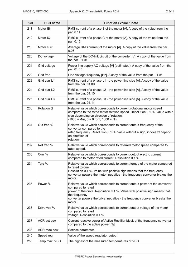
MFC810, MFC1000 Appendix C: Characteristic Points PCH C.3/11
PCH PCH name Function / value / note
211 Motor IB RMS current of a phase B of the motor [A]. A copy of the value from the par. 0.14
212 Motor IC RMS current of a phase C of the motor [A]. A copy of the value from the par. 0.15
213 Motor curr Average RMS current of the motor [A]. A copy of the value from the par. 0.06
220 DC voltage Voltage of the DC-link circuit of the converter [V]. A copy of the value from the par. 01.01
221 Grid voltage Power line supply AC voltage [V] (estimated). A copy of the value from the par. 01.05
222 Grid freq Line Voltage frequency [Hz]. A copy of the value from the par. 01.06
223 Grid curr L1 RMS current of a phase L1 - the power line side [A]. A copy of the value from the par. 01.09
224 Grid curr L2 RMS current of a phase L2 - the power line side [A]. A copy of the value from the par. 01.10
225 Grid curr L3 RMS current of a phase L3 - the power line side [A]. A copy of the value from the par. 01.11
230 Rotation % Relative value which corresponds to current rotational motor speed compared to the rated motor rotation speed. Resolution 0.1 %. Value with asign depending on direction of rotation:-1000 = -Nn, 0 = 0 rpm, 1000 = Nn
231 Out freq % Relative value which corresponds to current output frequency of the converter compared to therated frequency. Resolution 0.1 %. Value without a sign, it doesn’t depend on direction ofrotation.
232 Ref freq % Relative value which corresponds to referred motor speed compared to rated speed.
233 Curr % Relative value which corresponds to current output electric current compared to motor rated current. Resolution 0.1 %
234 Torq % Relative value which corresponds to current torque of the motor compared to rated torque.Resolution 0.1 %. Value with positive sign means that the frequency converter powers the motor, negative - the frequency converter brakes the motor.
235 Power % Relative value which corresponds to current output power of the converter compared to ratedpower of the drive. Resolution 0.1 %. Value with positive sign means that the frequencyconverter powers the drive, negative - the frequency converter breaks the motor.
236 Drive volt % Relative value which corresponds to current output voltage of the motor compared to ratedvoltage. Resolution 0.1 %.
237 ACR act pow Current reactive power of Active Rectifier block of the frequency converter compared to the active power [%]
238 ACR reac pow Service parameter
240 Speed reg Value of the speed regulator output
250 Temp max. VSD The highest of the measured temperatures of VSD
TWERD Power Electronics - www.twerd.pl
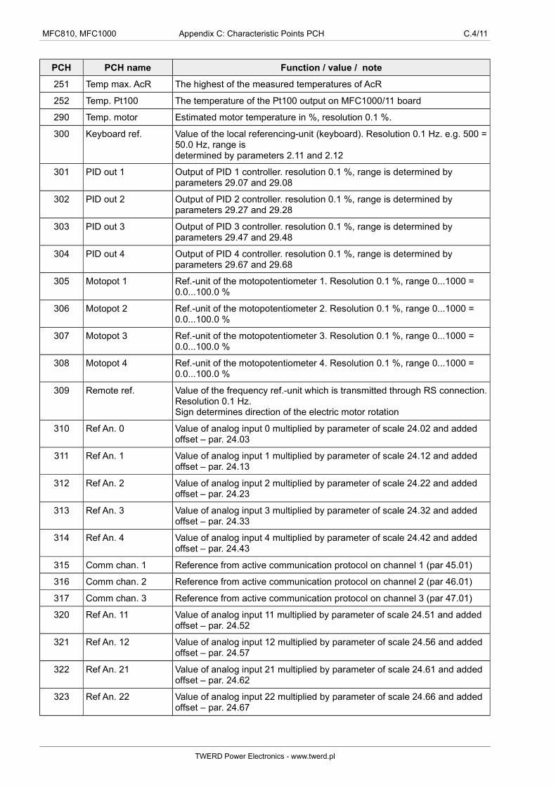
MFC810, MFC1000 Appendix C: Characteristic Points PCH C.4/11
PCH PCH name Function / value / note
251 Temp max. AcR The highest of the measured temperatures of AcR
252 Temp. Pt100 The temperature of the Pt100 output on MFC1000/11 board
290 Temp. motor Estimated motor temperature in %, resolution 0.1 %.
300 Keyboard ref. Value of the local referencing-unit (keyboard). Resolution 0.1 Hz. e.g. 500 =50.0 Hz, range isdetermined by parameters 2.11 and 2.12
301 PID out 1 Output of PID 1 controller. resolution 0.1 %, range is determined by parameters 29.07 and 29.08
302 PID out 2 Output of PID 2 controller. resolution 0.1 %, range is determined by parameters 29.27 and 29.28
303 PID out 3 Output of PID 3 controller. resolution 0.1 %, range is determined by parameters 29.47 and 29.48
304 PID out 4 Output of PID 4 controller. resolution 0.1 %, range is determined by parameters 29.67 and 29.68
305 Motopot 1 Ref.-unit of the motopotentiometer 1. Resolution 0.1 %, range 0...1000 = 0.0...100.0 %
306 Motopot 2 Ref.-unit of the motopotentiometer 2. Resolution 0.1 %, range 0...1000 = 0.0...100.0 %
307 Motopot 3 Ref.-unit of the motopotentiometer 3. Resolution 0.1 %, range 0...1000 = 0.0...100.0 %
308 Motopot 4 Ref.-unit of the motopotentiometer 4. Resolution 0.1 %, range 0...1000 = 0.0...100.0 %
309 Remote ref. Value of the frequency ref.-unit which is transmitted through RS connection.Resolution 0.1 Hz.Sign determines direction of the electric motor rotation
310 Ref An. 0 Value of analog input 0 multiplied by parameter of scale 24.02 and added offset – par. 24.03
311 Ref An. 1 Value of analog input 1 multiplied by parameter of scale 24.12 and added offset – par. 24.13
312 Ref An. 2 Value of analog input 2 multiplied by parameter of scale 24.22 and added offset – par. 24.23
313 Ref An. 3 Value of analog input 3 multiplied by parameter of scale 24.32 and added offset – par. 24.33
314 Ref An. 4 Value of analog input 4 multiplied by parameter of scale 24.42 and added offset – par. 24.43
315 Comm chan. 1 Reference from active communication protocol on channel 1 (par 45.01)
316 Comm chan. 2 Reference from active communication protocol on channel 2 (par 46.01)
317 Comm chan. 3 Reference from active communication protocol on channel 3 (par 47.01)
320 Ref An. 11 Value of analog input 11 multiplied by parameter of scale 24.51 and added offset – par. 24.52
321 Ref An. 12 Value of analog input 12 multiplied by parameter of scale 24.56 and added offset – par. 24.57
322 Ref An. 21 Value of analog input 21 multiplied by parameter of scale 24.61 and added offset – par. 24.62
323 Ref An. 22 Value of analog input 22 multiplied by parameter of scale 24.66 and added offset – par. 24.67
TWERD Power Electronics - www.twerd.pl
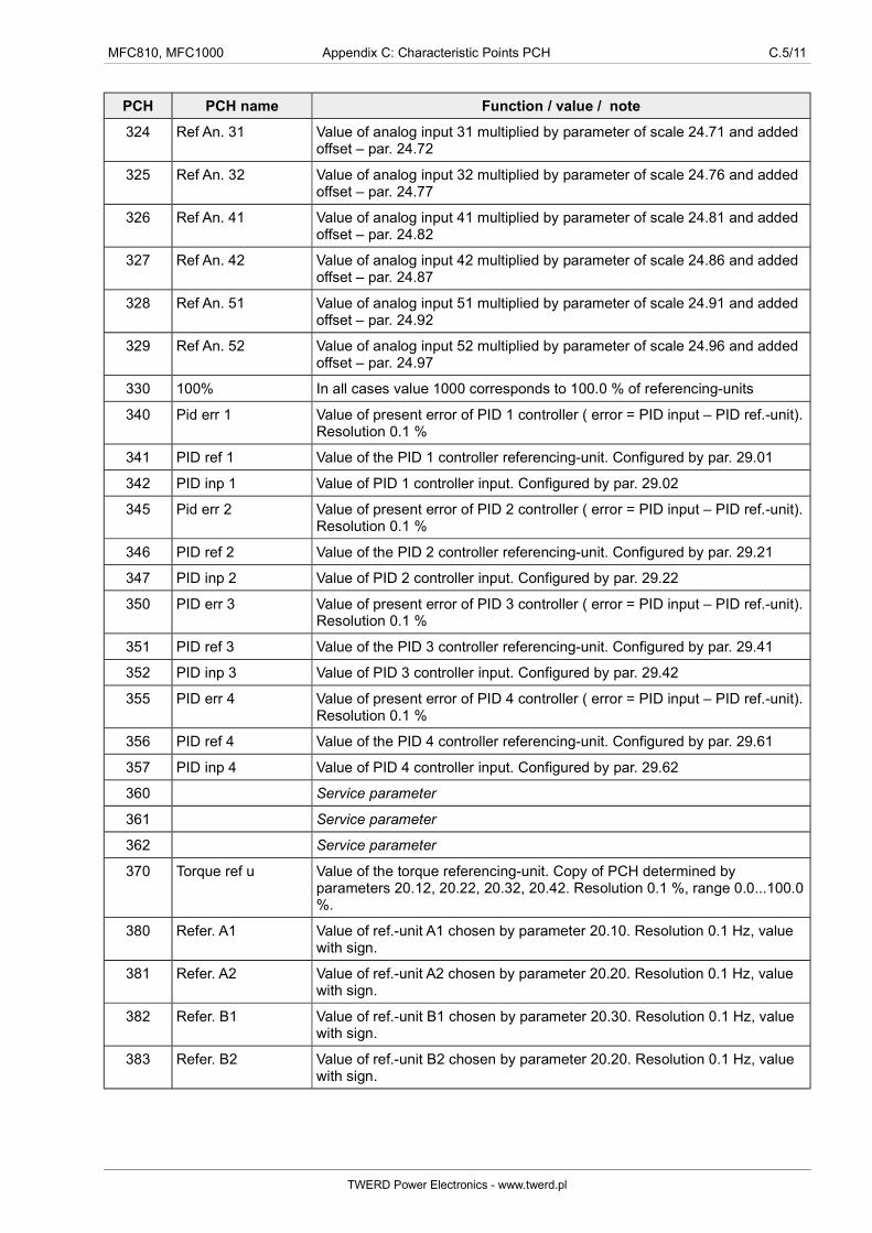
MFC810, MFC1000 Appendix C: Characteristic Points PCH C.5/11
PCH PCH name Function / value / note
324 Ref An. 31 Value of analog input 31 multiplied by parameter of scale 24.71 and added offset – par. 24.72
325 Ref An. 32 Value of analog input 32 multiplied by parameter of scale 24.76 and added offset – par. 24.77
326 Ref An. 41 Value of analog input 41 multiplied by parameter of scale 24.81 and added offset – par. 24.82
327 Ref An. 42 Value of analog input 42 multiplied by parameter of scale 24.86 and added offset – par. 24.87
328 Ref An. 51 Value of analog input 51 multiplied by parameter of scale 24.91 and added offset – par. 24.92
329 Ref An. 52 Value of analog input 52 multiplied by parameter of scale 24.96 and added offset – par. 24.97
330 100% In all cases value 1000 corresponds to 100.0 % of referencing-units
340 Pid err 1 Value of present error of PID 1 controller ( error = PID input – PID ref.-unit).Resolution 0.1 %
341 PID ref 1 Value of the PID 1 controller referencing-unit. Configured by par. 29.01
342 PID inp 1 Value of PID 1 controller input. Configured by par. 29.02
345 Pid err 2 Value of present error of PID 2 controller ( error = PID input – PID ref.-unit).Resolution 0.1 %
346 PID ref 2 Value of the PID 2 controller referencing-unit. Configured by par. 29.21
347 PID inp 2 Value of PID 2 controller input. Configured by par. 29.22
350 PID err 3 Value of present error of PID 3 controller ( error = PID input – PID ref.-unit).Resolution 0.1 %
351 PID ref 3 Value of the PID 3 controller referencing-unit. Configured by par. 29.41
352 PID inp 3 Value of PID 3 controller input. Configured by par. 29.42
355 PID err 4 Value of present error of PID 4 controller ( error = PID input – PID ref.-unit).Resolution 0.1 %
356 PID ref 4 Value of the PID 4 controller referencing-unit. Configured by par. 29.61
357 PID inp 4 Value of PID 4 controller input. Configured by par. 29.62
360 Service parameter
361 Service parameter
362 Service parameter
370 Torque ref u Value of the torque referencing-unit. Copy of PCH determined by parameters 20.12, 20.22, 20.32, 20.42. Resolution 0.1 %, range 0.0...100.0%.
380 Refer. A1 Value of ref.-unit A1 chosen by parameter 20.10. Resolution 0.1 Hz, value with sign.
381 Refer. A2 Value of ref.-unit A2 chosen by parameter 20.20. Resolution 0.1 Hz, value with sign.
382 Refer. B1 Value of ref.-unit B1 chosen by parameter 20.30. Resolution 0.1 Hz, value with sign.
383 Refer. B2 Value of ref.-unit B2 chosen by parameter 20.20. Resolution 0.1 Hz, value with sign.
TWERD Power Electronics - www.twerd.pl

MFC810, MFC1000 Appendix C: Characteristic Points PCH C.6/11
PCH PCH name Function / value / note
385 Refer. unit Output of control unit – the final value of the referencing unit, value with a sign determiningthe direction of rotation (plus = to the right, minus = to the left). Resolution 0.1 Hz.
390 F. const 1 Constant frequency number 1, Copy of parameter 23.06
391 F. const 2 Constant frequency number 2, Copy of parameter 23.07
392 F. const 3 Constant frequency number 3, Copy of parameter 23.08
393 F. const 4 Constant frequency number 4, Copy of parameter 23.09
394 F. const 5 Constant frequency number 5, Copy of parameter 23.10
395 F. const 6 Constant frequency number 6, Copy of parameter 23.11
396 F. const 7 Constant frequency number 7, Copy of parameter 23.12
397 F. const 8 Constant frequency number 8, Copy of parameter 23.13
398 F. const 9 Constant frequency number 9, Copy of parameter 23.14
399 F. const 10 Constant frequency number 10, Copy of parameter 23.15
400 F. const 11 Constant frequency number 11, Copy of parameter 23.16
401 F. const 12 Constant frequency number 12, Copy of parameter 23.17
402 F. const 13 Constant frequency number 13, Copy of parameter 23.18
403 F. const 14 Constant frequency number 14, Copy of parameter 23.19
404 F. const 15 Constant frequency number 15, Copy of parameter 23.20
410 Freq last Average frequency
411 Service parameter
412 Service parameter
420 Ref. user 1 Value of the user referencing-unit number 1
421 Ref. user 2 Value of the user referencing-unit number 2
422 Ref. user 3 Value of the user referencing-unit number 3
423 Ref. user 4 Value of the user referencing-unit number 4
424 Ref. user 5 Value of the user referencing-unit number 5
425 Ref. user 6 Value of the user referencing-unit number 6
426 Ref. user 7 Value of the user referencing-unit number 7
427 Ref. user 8 Value of the user referencing-unit number 8
428 Ref. user 9 Value of the user referencing-unit number 9
429 Ref. user 10 Value of the user referencing-unit number 10
430 Ref. A1 % Value corresponds to PCH.380 (referencing-unit A1) converted to relative value (compared torated motor frequency). Value without a sign, resolution 0.1 %.
431 Ref. A2% Value corresponds to PCH.381 (referencing-unit A2) converted to relative value (compared torated motor frequency). Value without a sign, resolution 0.1 %.
432 Ref. B1 % Value corresponds to PCH.382 (referencing-unit B1) converted to relative value (compared torated motor frequency). Value without a sign, resolution 0.1 %.
TWERD Power Electronics - www.twerd.pl

MFC810, MFC1000 Appendix C: Characteristic Points PCH C.7/11
PCH PCH name Function / value / note
433 Ref. B2 % Value corresponds to PCH.383 (referencing-unit B2) converted to relative value (compared torated motor frequency). Value without a sign, resolution 0.1 %.
434 Freq nom % Value corresponds to PCH.384 (referencing-unit) converted to relative value (compared to rated motor frequency). Value without a sign, resolution0.1 %.
435 Service parameter
436 Service parameter
440 Process n Speed of the process. Value of this PCH is a result of current rotation speed of the motor andscale factor determined with parameter 42.01. It serves for converting rotation speed to outputvalue (e.g. m/s).
460 Service parameter
461 Service parameter
462 Service parameter
500 Inactive Value always = L (logical 0)
501 Start local H = Local Control (control panel) permits STARTActive when 000 Keyboard is chosen as Start/Stop for active Control place (A1/A2/B1/B2)
502 Start remote H = Remote Control (digital inputs) permits STARTActive when 002 Remote 1 .. Remote 005 is chosen as Start/Stop for activeControl place (A1/A2/B1/B2)Note: This PCH do not determine rotation direction and only allows to start from digital inputs (remote 1..4) for active Control place (A1/A2/B1/B2)
503 Start comm H = Control through the connection RS allows START.Active when 001 Comm is chosen as Start/Stop for active Control place (A1/A2/B1/B2)
504 Keyboard dir Direction of operation with Local Control. 0 = determined with sign of referencing-unit, H =opposite (depends on pressing the key “Left” or “Right” on the control panel).
505 Digital dir Direction of operation with Remote Control. L = determined with sign of referencing-unit,H = opposite (depends on state of digital inputs and mode of Remote Start 002 Remote 1 .. 005 Remote 4).
506 Refer dir Ref.-unit sign (L = positive ref.-unit, H = negative ref.-unit)
507 Under fstop H = the converter is blocked because frequency referencing-unit is lower then STOP frequency determined by par. 21.10. This function will be switched on only in case of par. 21.11 = 001 Stop
508 Start allow L = general lack of permission to work, H = permission to work (yellow LEDon Control Panel is lighted up)
509 Rewers Operating direction at currently chosen control.L = is determined with a sign of referencing-unit,H = opposite.Equal to PCH.505 for remote control, PCH.504 for local control, L for RS control.
510Control A/B
Active when Control B is chosen
TWERD Power Electronics - www.twerd.pl
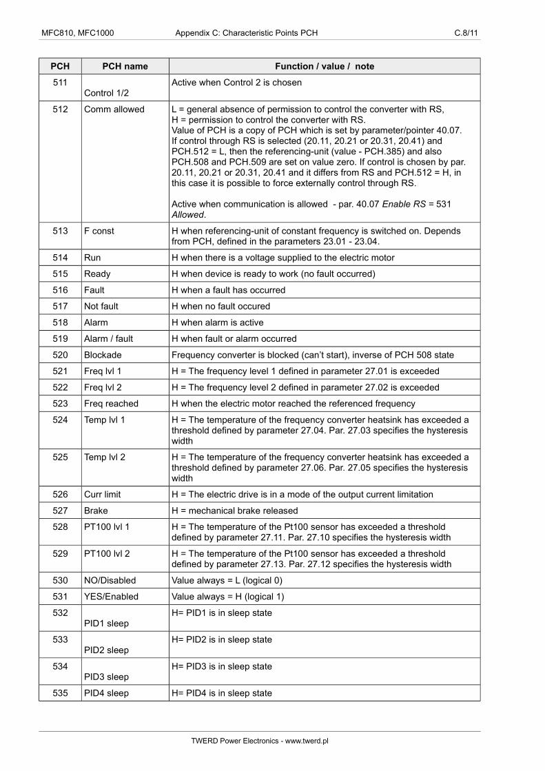
MFC810, MFC1000 Appendix C: Characteristic Points PCH C.8/11
PCH PCH name Function / value / note
511Control 1/2
Active when Control 2 is chosen
512 Comm allowed L = general absence of permission to control the converter with RS,H = permission to control the converter with RS.Value of PCH is a copy of PCH which is set by parameter/pointer 40.07.If control through RS is selected (20.11, 20.21 or 20.31, 20.41) and PCH.512 = L, then the referencing-unit (value - PCH.385) and also PCH.508 and PCH.509 are set on value zero. If control is chosen by par. 20.11, 20.21 or 20.31, 20.41 and it differs from RS and PCH.512 = H, in this case it is possible to force externally control through RS.
Active when communication is allowed - par. 40.07 Enable RS = 531 Allowed.
513 F const H when referencing-unit of constant frequency is switched on. Depends from PCH, defined in the parameters 23.01 - 23.04.
514 Run H when there is a voltage supplied to the electric motor
515 Ready H when device is ready to work (no fault occurred)
516 Fault H when a fault has occurred
517 Not fault H when no fault occured
518 Alarm H when alarm is active
519 Alarm / fault H when fault or alarm occurred
520 Blockade Frequency converter is blocked (can’t start), inverse of PCH 508 state
521 Freq lvl 1 H = The frequency level 1 defined in parameter 27.01 is exceeded
522 Freq lvl 2 H = The frequency level 2 defined in parameter 27.02 is exceeded
523 Freq reached H when the electric motor reached the referenced frequency
524 Temp lvl 1 H = The temperature of the frequency converter heatsink has exceeded a threshold defined by parameter 27.04. Par. 27.03 specifies the hysteresis width
525 Temp lvl 2 H = The temperature of the frequency converter heatsink has exceeded a threshold defined by parameter 27.06. Par. 27.05 specifies the hysteresis width
526 Curr limit H = The electric drive is in a mode of the output current limitation
527 Brake H = mechanical brake released
528 PT100 lvl 1 H = The temperature of the Pt100 sensor has exceeded a threshold defined by parameter 27.11. Par. 27.10 specifies the hysteresis width
529 PT100 lvl 2 H = The temperature of the Pt100 sensor has exceeded a threshold defined by parameter 27.13. Par. 27.12 specifies the hysteresis width
530 NO/Disabled Value always = L (logical 0)
531 YES/Enabled Value always = H (logical 1)
532PID1 sleep
H= PID1 is in sleep state
533PID2 sleep
H= PID2 is in sleep state
534PID3 sleep
H= PID3 is in sleep state
535 PID4 sleep H= PID4 is in sleep state
TWERD Power Electronics - www.twerd.pl
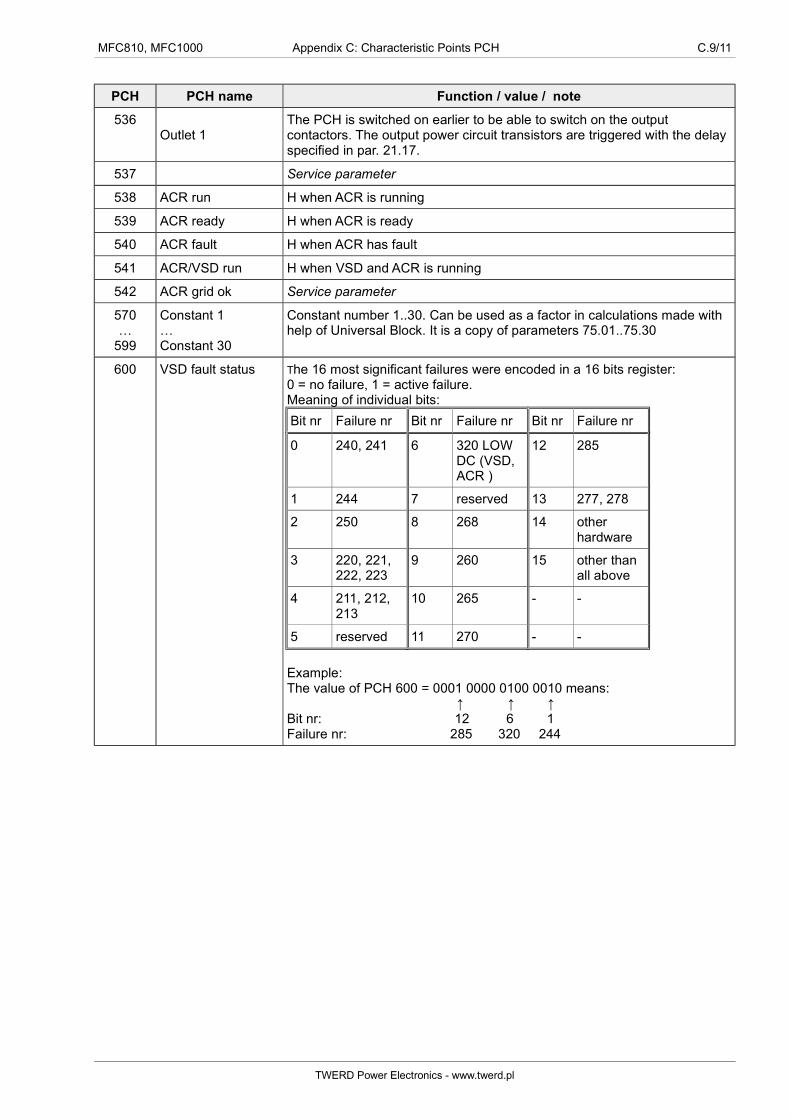
MFC810, MFC1000 Appendix C: Characteristic Points PCH C.9/11
PCH PCH name Function / value / note
536Outlet 1
The PCH is switched on earlier to be able to switch on the output contactors. The output power circuit transistors are triggered with the delay specified in par. 21.17.
537 Service parameter
538 ACR run H when ACR is running
539 ACR ready H when ACR is ready
540 ACR fault H when ACR has fault
541 ACR/VSD run H when VSD and ACR is running
542 ACR grid ok Service parameter
570K
599
Constant 1KConstant 30
Constant number 1..30. Can be used as a factor in calculations made with help of Universal Block. It is a copy of parameters 75.01..75.30
600 VSD fault status The 16 most significant failures were encoded in a 16 bits register:0 = no failure, 1 = active failure.Meaning of individual bits:
Bit nr Failure nr Bit nr Failure nr Bit nr Failure nr
0 240, 241 6 320 LOW DC (VSD, ACR )
12 285
1 244 7 reserved 13 277, 278
2 250 8 268 14 other hardware
3 220, 221, 222, 223
9 260 15 other than all above
4 211, 212, 213
10 265 - -
5 reserved 11 270 - -
Example:The value of PCH 600 = 0001 0000 0100 0010 means: ↑ ↑ ↑Bit nr: 12 6 1Failure nr: 285 320 244
TWERD Power Electronics - www.twerd.pl

MFC810, MFC1000 Appendix C: Characteristic Points PCH C.10/11
PCH PCH name Function / value / note
601 AcR fault status The 16 most significant failures were encoded in a 16 bit register:0 = no failure, 1 = active failure.Meaning of individual bits:
Bit nr Failure nr Bit nr Failure nr Bit nr Failure nr
0 340, 341 6 rezerwa 12 296
1 344 7 rezerwa 13 295
2 350 8 372 14 other hardware
3 330, 331 9 373 15 other than all above
4 311, 312, 313
10 321 - -
5 325, 326 11 370, 371 - -
Example:The value of PCH 601 = 0001 0001 0000 0010 means: ↑ ↑ ↑Bit no: 12 8 1Failure no: 296 372 344
630 AI0 fault H = lack of “living zero” on Analog input 0 (modes: 2...10V, 4...20mA)
632 Warning. Lack of the ''living zero''
H = a warning about the absence of a signal on analog inputs (1..4) in mode 2...10V and 4...20mA is active
650 Timeout 1 H when timeout on communication channel 1
651 Timeout 2 H when timeout on communication channel 2
652 Timeout 3 H when timeout on communication channel 3
700 ..749
PCH RS 1...50 Characteristic Points available do write thought RS. Therefore, it is possibleto control the process that takes data from these PCHs
750 ..769
PCH PD write After saving the value (eg via RS), the value is copied to a fixed parameter or PCH. Set by parameters 49.20-49.49.The value is not saved in the permanent memory of the inverter (eeprom)
770 ..789
PCH PD read Possibility of coping to a specific PCH a value from any parameter or other PCH. Set by parameters 49.0-49.19.
830 Seq state 1 .. 8 PLC controller. Sequencer system. Value H = active mode 1 .. 8(only one of the PCH.304...311 can assume value H at the same time and only if the sequencer is switched on)
838 SEKW NUMER SEQ
PLC controller. Sequencer system. Number of active mode. Value of this PCH can assumevalue 0...7.(0 = STATE 1...7 = STATE 8)
840 Multiplex 1 PLC controller. Output of Multiplexer 1. Value = L, when Multiplexer 1 is switched off.
841 Multiplex 2 PLC controller. Output of Multiplexer 2. Value = L, when Multiplexer 2 is switched off.
850 Output CSU PLC controller. Output Y of Curve Shaping Unit (CSU) X→Y
890 Timer 50 ms Signal of timer with 50ms period and 50% filling
TWERD Power Electronics - www.twerd.pl

MFC810, MFC1000 Appendix C: Characteristic Points PCH C.11/11
PCH PCH name Function / value / note
891 Timer 1s Signal of timer with 1s period and 50% filling
892 Timer 1min Signal of timer with 1min period and 50% filling
893 Timer 1 hour (t.1hour)
Signal of timer with 1 hour period and 50% filling
894 Timer 1ms Signal of timer with 1ms period and 50% filling
900..999 PLC out 1 .. 100 PLC controller. Output of the universal unit number 1..100. Depends on unitfunction. Value may be in the range from 0 to 65535.
MFC810_1000_PCH_EN_sv1.98r3_dv1.1.odt
TWERD Power Electronics - www.twerd.pl