Embed Size (px)
Citation preview

Euvis DST501-1
Rev 1
1
DST501-1 – High-Speed Modulated Arbitrary Chirping Module
PRODUCT DESCRIPTION The DST501-1 module generates modulated arbitrary chirping CW with frequency update rates up to 250 updates/microsecond (1/8 of the DDS clock rate). The output of the module is a single-ended RF output, OUT. The on-board SRAM provides 500K x 32-bit data memory. The DST can be controlled by a PC or can work alone with pre-stored linear-chirping waveform. The DDS clock input, DDSCK, can be operated up to 2 GHz with minimum power of 0 dBm. The carrier frequency input, LO, can be operated from 5 GHz up to 6 GHz. Both DDS clock and LO can be provided by two on-board PLLs and can be reconfigured to accept external clocks by simple hardware modifications. The PLL lock status of the DDS clock and LO are monitored by two LEDs.
KEY FEATURES: • 11-bit amplitude and 13-bit phase resolution DDS ROM • 32-bit frequency resolution with 8 clock update rate • 5 ~ 6 GHz LO frequency • 1 ~ 2 GHz DDS clock rate • High sideband and carrier suppression • 500K x 32-bit words memory depth with multiple userpage configuration • Minimum burst lengths of 256 ns in Triggered Burst Mode • Up to 2 millisecond chirping waveform at 2 GHz DDS clock • Programmable cyclic repetition: 1 ~ 65535 • Accepts external triggers and generates marker signal (programmable) • USB 2.0 compliant interface (other interfaces available upon request) • 17 W power consumption; Powered by a +12 VDC adapter (included) • User-friendly input data formats and various built-in chirping waveforms • Companion API and software drivers for easy system development

Euvis DST501-1
Rev 1
2
DETAILED SPECIFICATIONS
GENERAL
DDS Frequency Resolution 32 bits
Amplitude Resolution 11 bits
Phase Resolution 13 bits
Frequency Update Rate 1/8 of input clock
Running Modes Continuous Mode
Triggered Continuous Mode Triggered Burst Mode
User Interface Windows GUI, USB
API CLR-Support Languages
• Visual C++
• Visual C#
• Visual Basic
• Visual J#
Options Pre-Stored Linear-Chirp Startup Waveform
DDS INPUT CLOCK
Type Single-Ended Sinusoidal or Square Wave
Termination 50 Ohms
Connector SMA
Min Typ Max Units
Frequency Range 1000 2000 MHz
Power Level -3 0 +10 dBm
Return Loss 10 dB

Euvis DST501-1
Rev 1
3
LO INPUT CLOCK
Type Single-Ended Sinusoidal
Termination 50 Ohms
Connector SMA
Min Typ Max Units
Frequency Range 5 6 GHz
Power Level 0 +3 +6 dBm
Return Loss 10 dB
OUTPUT
Type Single-Ended
Termination 50 Ohms
Connectors SMA
Min Typ Max Units
Frequency Range 5 6 GHz
Power Level 0 dBm
IF Residual Phase Noise @ 1 kHz from Carrier with external DDS and LO clocks
-140 dBc / Hz
Return Loss 8 dB
Carrier Suppression 35 dBc
Sideband Suppression 35 dBc
Euvis DST501-1
Rev 1
4
WAVEFORMS
Max Waveform Length 522,240 frequency words
Max Number of User Pages 127
Minimum Waveform Length 64 frequency words in Free Run or Triggered Free Run modes
256 ns in Burst Mode Multi-Loop (number of frequency words depends on input clock and
frequency update rate)
TRIGGER
Connector SMA
Source External or Software
Trigger Input Threshold Levels Min Max Units
VIL 0 0.8 V
VIH 2.0 3.3 V
MARKER
Number of Markers 1
Marker Length Programmable
Minimum Marker Length 4 words
Marker Output Levels Min Typ Max Units
VOL 0 0 0.4 V
VOH 2.9 3.3 3.3 V

Euvis DST501-1
Rev 1
5
OPERATING CHARACTERISTICS
Min Typ Max Units
Operating Temperature 25 ° C
Power Supply Voltage 11.5 12.0 12.5 V
Power Supply Current @ 1.0 GSPS DDS Clock 1.4 A
Power Dissipation @ 1.0 GSPS DDS Clock 16.8 W

Euvis DST501-1
Rev 1
6
FUNCTIONAL OVERVIEW
The DST501-1 consists of two DDS chips to provide the baseband in-phase and quadrature waveforms. Both DDS’s can be independently configured as in-phase or quadrature phase. Three side-band configurations are available: upper side band (USB), lower-side band (LSB) and double-side band (DSB). Side-band configuration can be selected in GUI or by API methods. To derive an upper-side-band (USB) up-convert chirping, DDS A is the in-phase input into the modulator and DDS B is the quadrature input into the modulator. Both the DDS A and DDS B outputs go through a low-pass filter before entering into the modulator.
The LO frequency needs to be between 5 and 6 GHz. Both DDS clock and LO are provided by two on-board PPL-based VCO’s and can be configured to accept external clocks by simple hardware modifications. Two LVTTL (0/3.3 V square wave) 10-MHz reference clocks are required for the PLL’s. The PLL lock status of the DDS clock and LO are monitored by two LED’s. Reference clock frequency (10~100 MHz) can be specified upon order.

Euvis DST501-1
Rev 1
7
WAVEFORM GENERATION MODES
The module can be operated in three waveform generation modes: Free Run/Continuous mode, Triggered Free Run mode and Triggered Burst mode.
Continuous Mode
In Continuous mode, the module starts waveform generation by a Restart command from the GUI or API-based applications. Once the waveform starts, the module repeats the waveform continuously. There is no latency between two consecutive waveforms. The following waveform starts right after the end of the preceding waveform. The waveform generation can be aborted by an Abort command from the GUI or API-based applications.
Triggered Continuous Run Mode In Triggered Continuous mode, the operation manner is similar to that in Continuous mode except for the start of waveform. The waveform generation is initiated by a trigger signal. In order to accept the upcoming trigger signals, the module has to be armed prior to the instance of the trigger signals. Trigger signals happening before the module is armed will be ignored. An Arm command from the GUI or API-based applications can be used to arm the module. Once the module is armed, it waits for the trigger signal. The waveform generation starts after the falling edge of the trigger signal. The trigger signal can be mainly applied via the TRIGGER SMA connector or provided by a command Trigger via the GUI or API-based applications.
Euvis DST501-1
Rev 1
8
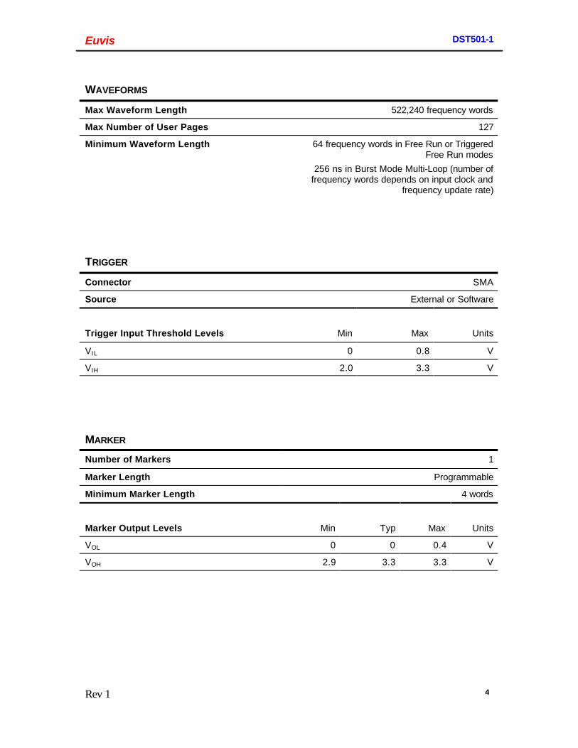
Triggered Burst Mode In Triggered Burst mode, the module starts waveform generation when it is armed and receives the trigger signal as in the Triggered Continuous mode. Instead of repeating continuously, the waveform starts, repeats, and stops after finite repetitions. The number of the repetitions can be specified by a property Loop Count via the GUI or the API-based applications. The Loop Count can be set from 1 to 255. Similarly, trigger signals happening before the waveform stops will be ignored. Once the waveform stops, the module will arm itself automatically and wait for the next trigger signal.

Euvis DST501-1
Rev 1
9
The following figure shows waveform generation for different Loop Counts: 1, 2, and 3.

Euvis DST501-1
Rev 1
10
0
Null NullStyled WaveformNull NullStyled Waveform
Delay
Delay + Data Length
Delay + Data Length + Padding Length
Data Length
Padding Length
Null NullStyled WaveformNull NullStyled Waveform Null NullStyled WaveformNull NullStyled Waveform
Styled WaveformStyled Waveform Styled WaveformStyled Waveform
Delay=0, Data Length = N * MUX factor
Waveform repetition; Loop Count = 2
BASEBAND WAVEFORM DETAILS The DST module equips with a 500K x 32-bit static memory chip. The maximum available chirping depth is 522,240 x 32 bit. Each 32-bit data represent a DDS output frequency, which lasts for 8 DDS clocks. All the time units used in common parameters (delay, data length, marker start/width, DDS reset T1, T2, and T3) in the GUI and API are in data point (8 DDS clocks.)
The minimum waveform length depends on the mode of the DST. In Continuous or Triggered Continuous Mode, the waveform length can be as short as 16 data points, which translates to about 64 ns at 2.0 GSPS. The minimum waveform length in Burst mode can be as short as 256 ns. The minimum waveform length is defined as an absolute time in Burst mode whereas the minimum waveform length in Continuous mode is defined in the number of data points. At 2.0 GHz, 256 ns translate to about 64 data points.
Styled waveforms can be generated with built-in linear chirping in GUI. There are three styles of the built-in waveforms: 1) linear upward chirp, 2) triangle chirp, 3) linear downward chirp. To generate the linear chirp, simply specify the chirping parameters: start, stop, and step frequencies. Arbitrary waveforms can be generated by using user-defined files or user-define bulk in GUI or API-based applications. Beside chirping parameters, common parameters are sued to composed the waveform in timely manner. The effects of delay and datalength parameters are shown in the following figure. MUX factor for DST is 4.
Markers are useful in synchronizing the waveforms. There is one marker available for the DST. The properties of the marker are Start, Width, Polarity, and Enable. The Start property specifies when the marker becomes active, and the Width property specifies how long the active marker lasts. However, because the markers are not multiplexed, their statuses are checked and updated only at each period of the Marker Sample Factor. A marker specified to start not at an integer multiple of the Marker Sample Factor will actually start at the next larger multiple of the Marker Sample Factor. A marker ceases to be active at the next integer multiple of the Marker Sample Factor at or after the position Start + Width.

Euvis DST501-1
Rev 1
11
The oscilloscope photos below demonstrate some of the capabilities of the DST. All three waveforms in the photos are chirping from 1/256 of the input clock frequency to 1/16 of the input clock frequency in steps of 1/256 of the input clock frequency. The three example waveforms differ in how many times they repeat this chirping segment. As you can see in Chart 1, each segment will take the waveform through 4.25 phase cycles.
Chart 1
The input clock in the waveforms are all 2.0 GHz, so for each segment of the waveform, the DST is chirping from 7.8125 MHz (2000MHz / 256) all the way up to 125 MHz (2000MHz / 16) in 7.8125 MHz steps for a total of 16 data points. There are 8 data points at the beginning of each waveform that is used for reset and where the phase and frequency is 0. The signal at the bottom of each photo is the Marker and goes high at the beginning of the waveform and stays high for the first 8 data points before going back low again.
Photo 1 In Photo 1, the DST is chirping 4 segments back to back for one complete waveform. The loop count is set to 1 so the DST runs the complete waveform one time when it senses a trigger. At

Euvis DST501-1
Rev 1
12
the end of the waveform, the module stops output and waits for the next trigger. The total waveform length is 72 data points (8 reset frequencies + 4 * (16 data points per segment) = 72), which translates to about 288 ns. Figure 1 shows the ideal waveform of Photo 1.
Figure 1
Chart 2 Each frequency “triangle” shown in red in Chart 2 represents one of the four chirping segments of the waveform in Photo 1. The phase is shown in blue. Recall that each segment will take the waveform through 4.25 phase cycles. After the first segment, the waveform has completed 4.25 phase cycles. After the second segment, the waveform has completed 8.5 phase cycles. After the third segment, the waveform has completed 12.75 phase cycles. Finally, after the fourth segment, the waveform has completed 17 phase cycles and is back at the original starting point. Figure 1 shows where the segments on the waveform are.

Euvis DST501-1
Rev 1
13
Figure 2
Photo 2 In Photo 2, the DST is chirping the same complete waveform as in Photo 1 but this time the loop count is set to 2. When the module senses a trigger, it will run the complete waveform two times in succession and at the end of the second complete waveform, the DST will stop output and wait for the next trigger. The total waveform length is about 544 ns at 2.0 GHz. Figure 3 shows ideal waveform of Photo 2.
Figure 3

Euvis DST501-1
Rev 1
14
Photo 3 Photo 3 demonstrates how short a waveform can be. This time, only one segment (1/256 of clock to 1/16 of clock in 1/256 of clock steps) is output as opposed to the 4 cycles in Photos 1 and 2. The first 8 data points consist of resets while the next 16 data points is the chirping segment. The total length is therefore 24 frequencies, which is only about 96 ns at 2.0 GHz. Figure 4 shows the ideal waveform of Photo 3.
Figure 4

Euvis DST501-1
Rev 1
15
Chart 2 Chart 2 shows the frequency and phase that the waveform in Photo 3 goes through. At the end of the waveform, it will have gone through 4.25 phase cycles.

Euvis DST501-1
Rev 1
16
BOARD DIAGRAM
DIMENSIONS
Length 7.75 inches
Width 5.50 inches
Height 0.7 inches with heatsink (nominal)

Euvis DST501-1
Rev 1
17
MOUNTHOLE LOCATIONS
X
(inches) Y
(inches)
0.125 0.125
5.375 0.125
0.125 3.875
5.375 3.875
0.125 7.625
Mountholes Origin at Bottom Left Corner
5.375 7.625
TERMINAL DESCRIPTION
Function I/O Signal
+12 V JACK Power Jack for +12 V DC Power DC
DDSCK DDS Clock Input Input RF
LO Local Oscillator Input Input RF
OUT Modulated Signal Output Output RF
TRIG Trigger; Used in Master Mode Input
SYNCIN Synchronize In; Used in Slave Mode Input
CKRST ASIC Clock Reset Input
MARKER1 Marker 1 Output
MARKER2 Marker 2 Output
SYNCOUT Synchronize Out; Used in Master Mode
Output
FPGA0 Auxiliary 0 Output
FPGA1 Auxiliary 1 Output
FPGA2 Auxiliary 2 Output
USB HEADER USB Control Bidirectional

Euvis DST501-1
Rev 1
18
Euvis Inc. Ordering Information: Email to: [email protected] Or call: (805) 583-9888 x108 Sales Department Or fax: (805) 583-9889 The information contained in this document is based on measured data. Characteristic data and other specifications are subject to change without notice. Customers are advised to confirm information in this advanced datasheet prior to using this information or placing the order. Euvis Inc. does not assume any liability arising from the application or use of any product or circuit described herein, neither does it convey any license under its patents or any other rights.