Embed Size (px)
Citation preview

1IEEE 802.3aeNew OrleansSeptember 12-14, 2000
DSP-Based Equalization forDSP-Based Equalization forOptical ChannelsOptical Channels
Feasibility of a VLSI ImplementationFeasibility of a VLSI Implementation
IEEE 802.3ae Meeting, New Orleans
September 12-14, 2000
Oscar Agazzi, Venu Gopinathan, and Keshab Parhi (Broadcom)
Kishore Kota (Cicada Semiconductor)
Abhijit Phanse (National Semiconductor)

2IEEE 802.3aeNew OrleansSeptember 12-14, 2000
IntroductionIntroduction
• This talk will discuss a receiver based on Decision-FeedbackEqualization (DFE) and its implementation using DSP techniques
• The proposed equalization technique is entirely done at the receiver. Itdoes not require any modification to the current PMD proposalsconsidered by 802.3ae
• It is not necessary to know the channel a priori, since the equalizer isadaptive and it automatically identifies the channel response
• The time constant for the equalizer adaptation is <<1ms (typically a fewmicroseconds at 10Gb/s data rates)
• The DSP-based architecture described in this presentation is onlyintended to be an example of a possible implementation. Alternativeimplementations are also possible and they will be investigated by thead-hoc group

3IEEE 802.3aeNew OrleansSeptember 12-14, 2000
Block Diagram of ReceiverBlock Diagram of Receiver
TIAHighpass
FilterProg. GainAmpifier
AGC
A/DNo 1
A/DNo 2
A/DNo 3
A/DNo 4
A/DNo 5
A/DNo 6
A/DNo 7
A/DNo 8
RETIMING ForwardEqualizer
DFE PCSSystem
Interface
TimingRecovery
fD
fC
fC fC
NOTE: Block diagram assumes a parallelization factor of 8

4IEEE 802.3aeNew OrleansSeptember 12-14, 2000
Block Diagram of EqualizerBlock Diagram of Equalizer
A/DInput
Z-1Z-1Z-1
Z-1Z-1Z-1
Σ
Σ
Σ
-
+
c0 c1 cN-1
d1 d2 dM
xn
an
yn
The eye patterns at Test Points A, B, and C from simulations at 3.125Gb/s and 10Gb/s will be shown in slides 11 through 13 and 16 through 18
NOTE: This is a conceptual block diagram. It does not reflecta parallel implementation
Test Point A
Test Point BTest Point C

5IEEE 802.3aeNew OrleansSeptember 12-14, 2000
Digital EqualizationDigital Equalization
• The Feedforward Equalizer (FFE) does mostly phase equalization so thatthe intersymbol interference (ISI) at its output is caused by the“postcursors” (samples occurring after the main sample) of the channelimpulse response
• The Decision-Feedback Equalizer (DFE) cancels the postcursor ISI
• It is possible to design the DFE in such a way that it can deal effectivelywith nonlinear ISI
6IEEE 802.3aeNew OrleansSeptember 12-14, 2000
Simulation EnvironmentSimulation Environment
• Pulse Preprocessing:âRemove DC biasâResample pulse with a sampling rate fsâConvolve with trapezoidal pulse with rise and fall times tsâConvolve with single-pole high-pass filter with cutoff frequency fh and with single-
pole low-pass filter with cutoff frequency fl. The high-pass filter models AC couplingin the TIA, and the low-pass filter models the bandwidth limitation of the TIA
âThe pulse is normalized by dividing it by the power of the calibration pulse andmultiplying it by the assumed launch power
• Phase selection and decimation to the symbol rate:âThe pulse is decimated to the symbol rate using as sampling phase the phase that
maximizes the energy of the decimated pulse
• Equalization:âThe coefficients of the FFE and DFE are computed using the Minimum Mean
Squared Error algorithm (Ref.[4], pp. 521-524)

7IEEE 802.3aeNew OrleansSeptember 12-14, 2000
Assumptions in SimulationsAssumptions in Simulations
• The quasi-linear approximation (Ref.[1]) holds:âThe optical power at the input of the receiver can be represented as the
convolution of the transmitted bits with an impulse response that modelsthe attenuation and dispersion of the fiber
âThis requirement can be relaxed by using nonlinear equalizationtechniques
• Any time variations of the channel response aresufficiently slow that they can be tracked by theadaptation algorithm:
âThe time constant of any time dependence of the channel response mustbe equal to or larger than 1 microsecond

8IEEE 802.3aeNew OrleansSeptember 12-14, 2000
Parameters of SimulationsParameters of Simulations
Symbol Rate (fB)Time Resolution of Simulation (1/fs)Rise and Fall Times of Tx. PulseFull-width at half maximum (FWHM)TIA Bandwidth (fl)TIA High-Pass Corner (fh)Launch powerResponsivity of photodetectorTIA Input-Referred Noise Current(includes RIN, modal noise, shot noise, and thermal noise of TIA)Probability Density Function of the NoisePower Spectral Density of the NoiseNumber of FFE TapsNumber of DFE Taps
10/3.125 Gbaud5ps35ps65ps0.75fB2MHz-9dBm0.7Amp/Watt1µA
GaussianWhite86

9IEEE 802.3aeNew OrleansSeptember 12-14, 2000
Error Rate Error Rate vsvs. Electrical SNR for Binary. Electrical SNR for BinaryModulationModulation

10IEEE 802.3aeNew OrleansSeptember 12-14, 2000
Fiber Impulse ResponseFiber Impulse Response(An example of DMD pulse from 802.3z database; 1310nm, 320m MMF)(An example of DMD pulse from 802.3z database; 1310nm, 320m MMF)

11IEEE 802.3aeNew OrleansSeptember 12-14, 2000
Eye Pattern at Input of A/D (3.125Gb/s)Eye Pattern at Input of A/D (3.125Gb/s)(An example of DMD pulse from 802.3z database; 1310nm, 320m MMF)(An example of DMD pulse from 802.3z database; 1310nm, 320m MMF)
Test Point A

12IEEE 802.3aeNew OrleansSeptember 12-14, 2000
Eye Pattern at Output of A/D (3.125Gb/s)Eye Pattern at Output of A/D (3.125Gb/s)(An example of DMD pulse from 802.3z database; 1310nm, 320m MMF)(An example of DMD pulse from 802.3z database; 1310nm, 320m MMF)
Test Point B

13IEEE 802.3aeNew OrleansSeptember 12-14, 2000
Equalized Eye Pattern at Input of Equalized Eye Pattern at Input of SlicerSlicer (3.125Gb/s) (3.125Gb/s)(An example of DMD pulse from 802.3z database; 1310nm, 320m MMF)(An example of DMD pulse from 802.3z database; 1310nm, 320m MMF)
SNR at the Slicer = 28dB - BER <<
Test Point C

14IEEE 802.3aeNew OrleansSeptember 12-14, 2000
FFE Coefficients - 3.125Gb/sFFE Coefficients - 3.125Gb/s

15IEEE 802.3aeNew OrleansSeptember 12-14, 2000
DFE Coefficients - 3.125Gb/sDFE Coefficients - 3.125Gb/s

16IEEE 802.3aeNew OrleansSeptember 12-14, 2000
Eye Pattern at Input of A/D (10Gb/s)Eye Pattern at Input of A/D (10Gb/s)(An example DMD pulse from 802.3z database; 1310nm, 320m MMF)(An example DMD pulse from 802.3z database; 1310nm, 320m MMF)
Test Point A

17IEEE 802.3aeNew OrleansSeptember 12-14, 2000
Eye Pattern at Output of A/D (10Gb/s)Eye Pattern at Output of A/D (10Gb/s)(An example of DMD pulse from the 802.3z database; 1310nm, 320m MMF)(An example of DMD pulse from the 802.3z database; 1310nm, 320m MMF)
Test Point B
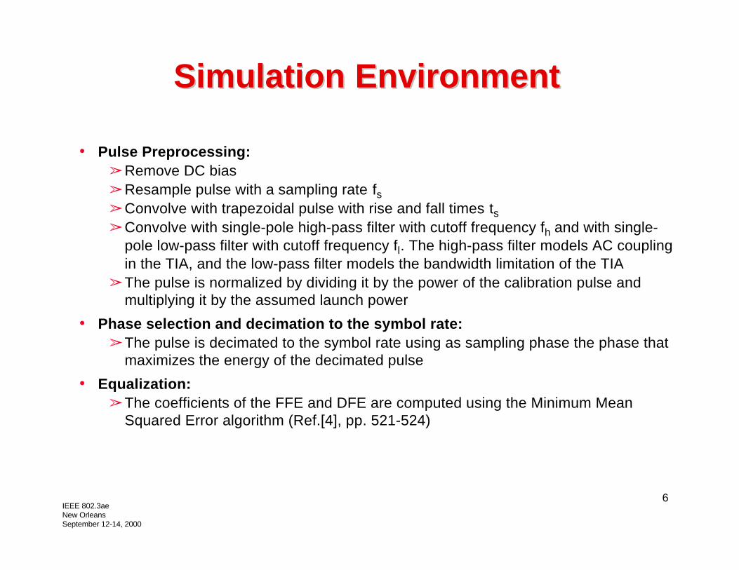
18IEEE 802.3aeNew OrleansSeptember 12-14, 2000
Equalized Eye Pattern at Input of Equalized Eye Pattern at Input of SlicerSlicer (10Gb/s) (10Gb/s)(An example of DMD pulse from the 802.3z database; 1310nm, 320m MMF)(An example of DMD pulse from the 802.3z database; 1310nm, 320m MMF)
SNR at the Slicer = 19dB - BER = 10-19
Test Point C

19IEEE 802.3aeNew OrleansSeptember 12-14, 2000
FFE Coefficients - 10Gb/sFFE Coefficients - 10Gb/s
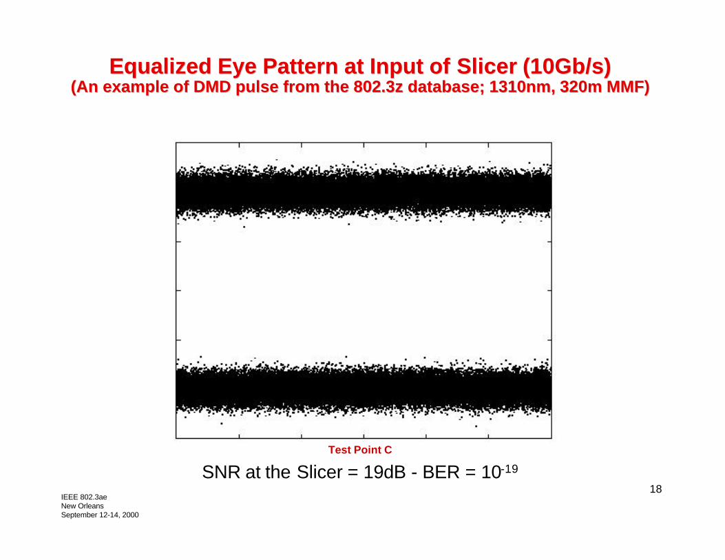
20IEEE 802.3aeNew OrleansSeptember 12-14, 2000
DFE Coefficients - 10Gb/sDFE Coefficients - 10Gb/s

21IEEE 802.3aeNew OrleansSeptember 12-14, 2000
DMD Channel ResponseDMD Channel Response
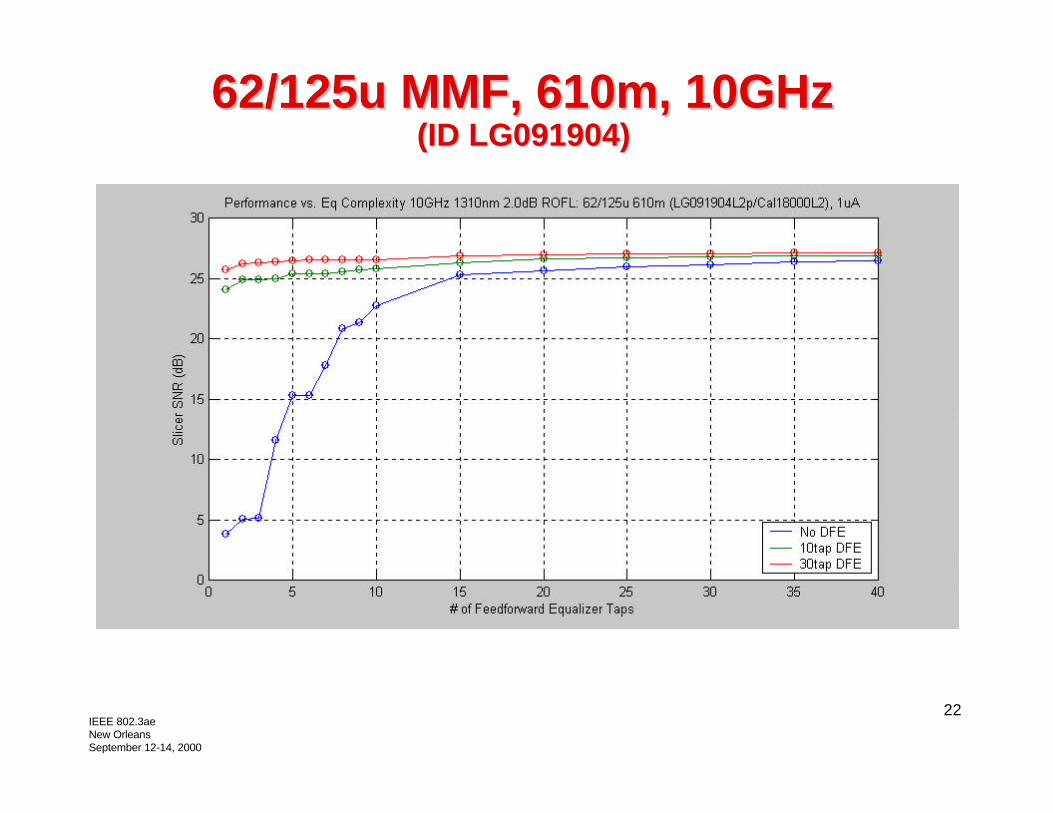
22IEEE 802.3aeNew OrleansSeptember 12-14, 2000
62/125u MMF, 610m, 10GHz62/125u MMF, 610m, 10GHz(ID LG091904)(ID LG091904)

23IEEE 802.3aeNew OrleansSeptember 12-14, 2000
62/125u MMF, 610m, 10GHz62/125u MMF, 610m, 10GHz(ID LG091904)(ID LG091904)
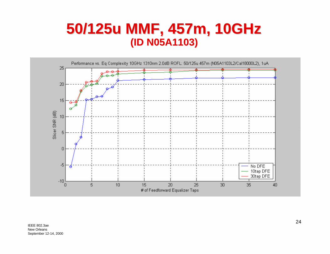
24IEEE 802.3aeNew OrleansSeptember 12-14, 2000
50/125u MMF, 457m, 10GHz50/125u MMF, 457m, 10GHz(ID N05A1103)(ID N05A1103)

25IEEE 802.3aeNew OrleansSeptember 12-14, 2000
50/125u MMF, 457m, 10GHz50/125u MMF, 457m, 10GHz(ID N05A1103)(ID N05A1103)
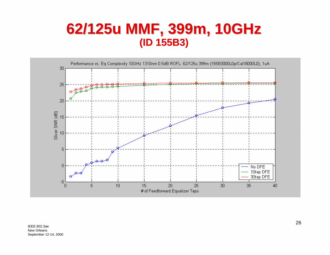
26IEEE 802.3aeNew OrleansSeptember 12-14, 2000
62/125u MMF, 399m, 10GHz62/125u MMF, 399m, 10GHz(ID 155B3)(ID 155B3)

27IEEE 802.3aeNew OrleansSeptember 12-14, 2000
62/125u MMF, 399m, 10GHz62/125u MMF, 399m, 10GHz(ID 155B3)(ID 155B3)

28IEEE 802.3aeNew OrleansSeptember 12-14, 2000
VLSI ImplementationVLSI Implementation
• Parallel FFE (Straightforward)
• DFE parallelization requires loop reformulationfollowed by application of look-ahead
• 8 FFE and 6 DFE taps assumed. This is the samenumber used in the simulations reported in slides 11through 20. No attempt was made to optimize thenumber of taps
• Interleaved A/D converter
• Power and area estimates
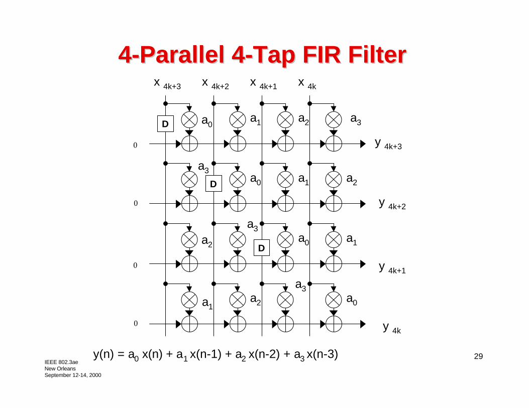
29IEEE 802.3aeNew OrleansSeptember 12-14, 2000
4-Parallel 4-Tap FIR Filter4-Parallel 4-Tap FIR Filter
D
D
D
0
0
0
0
y 4k+3
y 4k+2
y 4k+1
y 4k
x 4k+3 x 4k+2 x 4k+1 x 4k
a0
a0
a0
a0
a1
a1
a1
a2
a2
a3
a3
a3
a3
a2
a2a1
y(n) = a0 x(n) + a1 x(n-1) + a2 x(n-2) + a3 x(n-3)
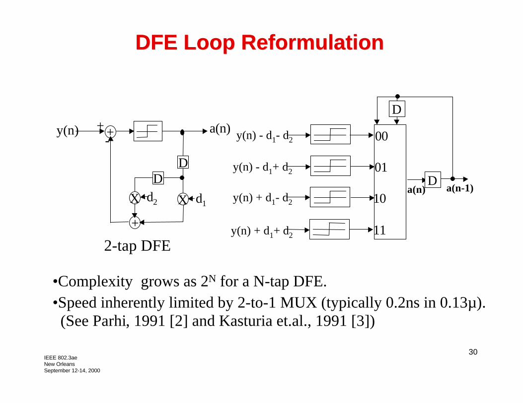
30IEEE 802.3aeNew OrleansSeptember 12-14, 2000
DFE Loop ReformulationDFE Loop Reformulation
•Complexity grows as 2N for a N-tap DFE.•Speed inherently limited by 2-to-1 MUX (typically 0.2ns in 0.13µ). (See Parhi, 1991 [2] and Kasturia et.al., 1991 [3])
2-tap DFE
01
00
10
11
D
D
a(n) a(n-1)
y(n) - d1- d2
y(n) - d1+ d2
y(n) + d1- d2
y(n) + d1+ d2
+
D
X
+
DX d2 d1
-+y(n) a(n)

31IEEE 802.3aeNew OrleansSeptember 12-14, 2000
2-Parallel Implementation2-Parallel Implementation
•Complexity ∼ L 2N for L-Parallel and N-tap DFE.
•Speed bounded by L multiplexers (L ≤ 5 for 1GHz clock).
a(2k)
y(2k) - d1- d2
y(2k) - d1+ d2
y(2k) + d1- d2
y(2k) + d1+ d2
a(2k+1)
y(2k+1) - d1- d2
y(2k+1) - d1+ d2
y(2k+1) + d1- d2
y(2k+1) + d1+ d2
D01
00
10
11
01
00
10
11
D

32IEEE 802.3aeNew OrleansSeptember 12-14, 2000
Look-AheadLook-Ahead
a(n) = f1(n)a(n-1)a(n-2) + f2(n)a(n-1)a(n-2) + f3(n)a(n-1)a(n-2) + f4(n)a(n-1)a(n-2) = [f1(n)f1(n-1) + f3(n)f1(n-1)] a(n-2)a(n-3) + [f1(n)f2(n-1) + f3(n)f2(n-1)] a(n-2)a(n-3) + [f2(n)f3(n-1) + f4(n)f3(n-1)] a(n-2)a(n-3) + [f2(n)f4(n-1) + f4(n)f4(n-1)] a(n-2)a(n-3)
• One step of look-ahead requires one column of multiplexers.
• Obtained by substituting expressions for a(n-1) and a(n-1) in terms of a(n-2) and a(n-3).

33IEEE 802.3aeNew OrleansSeptember 12-14, 2000
Highly Parallel ImplementationHighly Parallel Implementation
• Apply Look-Ahead to Reformulated DFE and eliminate dependence of a(n) on a(n-1).
• When unfolded or unrolled by factor 2 leads to 2-parallel architecture with a critical path of 1 multiplexer delay.• Loop critical path = L/2 multiplexer delays.• Attractive for L ≤ 10 for a critical path to be less than 5 MUX delays.
00
01
10
11
10
01
10
01
D
D
D
D
2D
D
y(n) - d1 - d2
y(n) - d1 + d2
y(n) + d1 - d2
y(n) + d1 + d2
a(n-2)

34IEEE 802.3aeNew OrleansSeptember 12-14, 2000
6-bit, Interleaved ADC6-bit, Interleaved ADC
• First T/H determines the dynamic performance of theADC
âSamples at 10GHz.âNeed at least 6-bits of precision.
• Gain and offset errors between the channels aredigitally corrected.
ADC06
ADC16
ADC76
fs0
fs7
fs0fs1
fclock

35IEEE 802.3aeNew OrleansSeptember 12-14, 2000
10-GHz Track & Hold10-GHz Track & Hold
• Required 6bits of S/(N+D)
• Makes the ADC sample a ‘held’ signalâSignificantly relieves the dynamic requirements of the ADC.
Technology:
• 90GHz peak-fT SiGe technology
• 0.18u linewidth
• 1.8V supply
10GHz
Analog in
SwitchBuffer

36IEEE 802.3aeNew OrleansSeptember 12-14, 2000
Simulated PerformanceSimulated Performance
• 6-bit THD for 10GHz sampling of a full-scale (800mVp-p) signal.
THD of SiGe S/H (10GHz sampling)
0
10
20
30
40
50
60
0.0 2.0 4.0 6.0 8.0 10.0
Input Frequency (GHz)
THD
(dB
)
THD6-bits

37IEEE 802.3aeNew OrleansSeptember 12-14, 2000
Area and Power EstimatesArea and Power Estimates(10-Gig Serial)(10-Gig Serial)
•Assumed technology: Digital 0.13µm CMOS, Analog 0.18µm SiGe•Receiver uses 8-tap FFE and 6-tap DFE (same as in simulations)•DSP parallelization factor 8 (1.25 GHz clock speed)•ADC parallelization factor 8
• 16-Parallel Implementation requires more area but slower clock and lower clock power.
Component Area PowerAnalog ---- 0.45 Watts
DSP 1mm2 0.80 WattsTotal ---- ∼ 1.25Watts

38IEEE 802.3aeNew OrleansSeptember 12-14, 2000
ConclusionsConclusions
• Digital equalization has potential to overcome DMD problems inmultimode fibers and extend link range
• Parallel processing makes it possible to implement advanceddigital equalization at symbol rates as high a 10GBaud
• Advanced CMOS and SiGe technologies offer great promise forinterleaved A/D converters at the required sampling rates
• In addition, advanced VLSI technologies offer potential for lowcost, low power implementations
• However, more studies are needed to conclusively establish thefeasibility of equalization for optical channels

39IEEE 802.3aeNew OrleansSeptember 12-14, 2000
ReferencesReferences
1. S.D.Personick, “Baseband Linearity and Equalization in Fiber Optic Digital Communication Systems,” Bell System Technical Journal, Vol.52, No.7, Sept.1973, pp.1175-1194
2. K.K.Parhi, “Pipelining in Algorithms with Quantizer Loops,” IEEE Transactions on Circuits and Systems, Vol.38, No.7, July 1991, pp.745-754
3. S.Kasturia and J.H.Winters, “Techniques for High-Speed Implementation of Nonlinear Cancellation,” IEEE Journal on Selected Areas in Communications, Vol.9, No.5, June 1991, pp.711-717
4. E.A.Lee and D.G.Messerschmitt, “Digital Communication,” 2nd edition, Kluwer Academic Publishers, 1994