Embed Size (px)
Citation preview

CAT#1918_TitlePage 7/21/03 2:34 PM Page 1
CRC PR ESSBoca Raton London New York Washington, D.C.
DSP-BASEDELECTROMECHANICAL
MOTION CONTROL
Hamid A. ToliyatSteven Campbell
Texas A&M UniversityDepartment of Electrical Engineering
College Station, Texas
Copyright © 2004 CRC Press, LLC

This book contains information obtained from authentic and highly regarded sources. Reprinted materialis quoted with permission, and sources are indicated. A wide variety of references are listed. Reasonableefforts have been made to publish reliable data and information, but the author and the publisher cannotassume responsibility for the validity of all materials or for the consequences of their use.
Neither this book nor any part may be reproduced or transmitted in any form or by any means, electronicor mechanical, including photocopying, microfilming, and recording, or by any information storage orretrieval system, without prior permission in writing from the publisher.
The consent of CRC Press LLC does not extend to copying for general distribution, for promotion, forcreating new works, or for resale. Specific permission must be obtained in writing from CRC Press LLCfor such copying.
Direct all inquiries to CRC Press LLC, 2000 N.W. Corporate Blvd., Boca Raton, Florida 33431.
Trademark Notice:
Product or corporate names may be trademarks or registered trademarks, and areused only for identification and explanation, without intent to infringe.
Visit the CRC Press Web site at www.crcpress.com
© 2004 by CRC Press LLC
No claim to original U.S. Government worksInternational Standard Book Number 0-8493-1918-8
Library of Congress Card Number 2003058462Printed in the United States of America 1 2 3 4 5 6 7 8 9 0
Printed on acid-free paper
Library of Congress Cataloging-in-Publication Data
Toliyat, Hamid A.DSP-Based electromechanical motion control / by Hamid A. Toliyat and Steven Campbell.
p. cm.-- (Power electronics and applications series)Includes bibliographical references and index.ISBN 0-8493-1918-8 (alk. paper)1. Digital control systems. 2. Electromechanical devices. 3. Signal processing--Digital
techniques. I. Campbell, Steven (Steven Gerard), 1979- II. Title. III. Series.
TJ223.M53.T64 2003629.8—dc22 2003058462
1918 disclaimer Page 1 Tuesday, August 19, 2003 12:15 PM
Copyright © 2004 CRC Press, LLC

To my wife Mina, and my sons Amir and Mohammad for their love
and patience while this book was being prepared.
To my parents for their continuous support and encouragement.
- H.T.
Copyright © 2004 CRC Press, LLC

PREFACE
This book was written to provide a general application guide for students and
engineers of all disciplines who want to begin utilizing a Digital Signal Processor (DSP) for the task of electromechanical motion control. While the act of learning to program and use the DSP itself is not overly difficult, utilizing the DSP in applications such as motor control can sometimes seem challenging to the first-time user.
Full mastery of all the topics and concepts presented in this text would take years of study and knowledge from many areas of engineering and science. For this reason, we will attempt to survey each topic, giving readers a basic understanding of each topic without going into great depth. We will thus leave it to the reader for in-depth study of particular topics of interest.
So why would we choose to integrate a DSP into a motion control system? Well, the advantages of such a design are numerous. DSP-based control gives us a large degree of freedom in developing computationally extensive algorithms that would otherwise be very difficult or impossible without a DSP. Advanced control algorithms can sometimes drastically increase the performance and efficiency of the electromechanical system being controlled.
For example, consider a typical Heating-Ventilation-and-Air-Conditioning (HVAC) system. A standard HVAC system contains at least three electric motors: compressor motor, condenser fan motor, and the air handler fan motor. Typically, indoor temperature is controlled by simply cycling (turning on and off) the system. This control method puts unnecessary wear on system components and is inefficient. An advanced motor drive system incorporating DSP control could continuously adjust both the air-conditioner compressor speed and indoor fan to maintain the desired temperature and optimal system performance. This control scheme would be much more energy efficient and could extend the operational lifespan of the system.
We will start by visiting the LF2407 DSP processor. Device functionality, integrated components, memory, and assembly programming will be covered. Several laboratory exercises will help the reader practice the information presented in each chapter. After several chapters are presented on the DSP, more advanced topics are presented involving several real-world applications in the area of motion control and motor drives.
Copyright © 2004 CRC Press, LLC

ACKNOWLEDGMENTS
As most readers can imagine, creating a book is no trivial task. Besides the authors listed on the cover of each book, there are usually many others who give their time and knowledge. These contributions range from the writing of a chapter to simply proofreading the book for mistakes. This book is no exception. There are many people I would like to thank who made invaluable contributions to the creation of this book.
During the past two years that this book was in development, the many undergraduate students who took my “DSP-Based Electromechanical Motion Control Devices” course in the Department of Electrical Engineering at Texas A&M University provided invaluable feedback on the material. I am in debt to all of them.
I would also like to extend my gratitude to Texas Instruments for permitting me to use the materials in its manuals. I would also like to extend a special acknowledgment to Gene Frantz and Christina Peterson from Texas Instruments, whose help and support for materializing this book were fundamental.
Several individuals, including my past and present graduate students, have contributed to this book. They are as follows: Sebastien Gay, Dr. Masoud Hajiaghajni - Chapter 7; Dr. Lei Hao and Leila Parsa - Chapters 8, 9, and 12; Mehdi Abolhassani - Chapter 10; Nasser Qahtani - Chapter 11; Peyman Niazi - Chapter 13; Sang-shin Kwak - Chapter 15; and Baris Ozturk the Appendix.
Dr. Babak Fahimi of University of Missouri-Rolla wrote Chapter 14 and Dr. Syed Madani of the University of Puerto Rico-Mayaguez contributed to Chapter 7. Rebecca Morrison proofread several chapters.
I would also like to thank Nora Konopka, Helena Redshaw, Susan Fox of CRC Press for their patience and support while this book was being prepared. Hamid A. Toliyat College Station, TX
Copyright © 2004 CRC Press, LLC

TABLE OF CONTENTS
Chapter 1 Introduction to the TMSLF2407 DSP Controller ....................................1
1.1 Introduction.......................................................................................1 1.2 Brief Introduction to Peripherals.......................................................3 1.3 Types of Physical Memory ...............................................................5 1.4 Software Tools..................................................................................6
Chapter 2 C2xx DSP CPU and Instruction Set ......................................................19
2.1 Introduction to the C2xx DSP Core and Code Generation .............19 2.2 The Components of the C2xx DSP Core ........................................19 2.3 Mapping External Devices to the C2xx Core and the Peripheral
Interface ...................................................................................21 2.4 System Configuration Registers......................................................22 2.5 Memory...........................................................................................26 2.6 Memory Addressing Modes............................................................31 2.7 Assembly Programming Using the C2xx DSP Instruction Set .......36
Chapter 3 General Purpose Input/Output (GPIO) Functionality............................49
3.1 Pin Multiplexing (MUX) and General Purpose I/O Overview .......49 3.2 Multiplexing and General Purpose I/O Control Registers ..............50 3.3 Using the General Purpose I/O Ports ..............................................57 3.4 General Purpose I/O Exercise .........................................................58
Chapter 4 Interrupts on the TMS320LF2407.........................................................61
4.1 Introduction to Interrupts ................................................................61 4.2 Interrupt Hierarchy .........................................................................61 4.3 Interrupt Control Registers .............................................................64 4.4 Initializing and Servicing Interrupts in Software ............................70 4.5 Interrupt Usage Exercise.................................................................75
Chapter 5 The Analog-to-Digital Converter (ADC) ..............................................77
5.1 ADC Overview ...............................................................................77 5.2 Operation of the ADC.....................................................................78 5.3 Analog to Digital Converter Usage Exercise ..................................98
Chapter 6 The Event Managers (EVA, EVB) ......................................................101
6.1 Overview of the Event Manager (EV) ..........................................101 6.2 Event Manager Interrupts .............................................................102 6.3 General Purpose (GP) Timers .......................................................115 6.4 Compare Units ..............................................................................134 6.5 Capture Units and Quadrature Encoded Pulse (QEP) Circuitry....147 6.6 General Event Manager Information ............................................158 6.7 Exercise: PWM Signal Generation ...............................................161
Copyright © 2004 CRC Press, LLC
Chapter 7 DSP-Based Implementation of DC-DC Buck-Boost Converters ........163 7.1 Introduction...................................................................................163 7.1 Converter Structure.......................................................................163 7.2 Continuous Conduction Mode ......................................................164 7.3 Discontinuous Conduction Mode..................................................165 7.4 Connecting the DSP to the Buck-Boost Converter .......................165 7.5 Controlling the Buck-Boost Converter .........................................168 7.6 Main Assembly Section Code Description ...................................171 7.7 Interrupt Service Routine..............................................................173 7.8 The Regulation Code Sequences...................................................175 7.9 Results...........................................................................................179
Chapter 8 DSP-Based Control of Stepper Motors ...............................................183
8.1 Introduction...................................................................................183 8.2 The Principle of Hybrid Stepper Motor ........................................183 8.3 The Basic Operation .....................................................................184 8.4 The Stepper Motor Drive System .................................................188 8.5 The Implementation of Stepper Motor Control System Using the
LF2407 DSP ................................................................................ 190 8.6 The Subroutine of Speed Control Module ....................................191 Reference ......................................................................................192
Chapter 9 DSP-Based Control of Permanent Magnet Brushless DC Machines...193
9.1 Introduction...................................................................................193 9.2 Principles of the BLDC Motor......................................................195 9.3 Torque Generation ........................................................................195 9.4 BLDC Motor Control System.......................................................196 9.5 Implementation of the BLDC Motor Control System Using the
LF2407..........................................................................................200 Chapter 10 Clarke’s and Park’s Transformations ................................................209
10.1 Introduction...................................................................................209 10.2 Clarke’s Transformation ...............................................................209 10.3 Park’s Transformation ..................................................................210 10.4 Transformations Between Reference Frames ...............................212 10.5 Field Oriented Control (FOC) Transformations............................213 10.6 Implementing Clarke’s and Park’s Transformations on the LF240X............................................................................. 214 10.7 Conclusion ....................................................................................222 References.....................................................................................222
Chapter 11 Space Vector Pulse Width Modulation .............................................223
11.1 Introduction...................................................................................223 11.2 Principle of Constant V/Hz Control for Induction Motors............223 11.3 Space Vector PWM Technique.....................................................224 11.4 DSP Implementation.....................................................................232
Copyright © 2004 CRC Press, LLC

References.....................................................................................240 Chapter 12 DSP-Based Control of Permanent Magnet Synchronous Machines..241
12.1 Introduction...................................................................................241 12.2 The Principle of the PMSM ..........................................................241 12.3 PMSM Control System.................................................................244 12.4 Implementation of the PMSM System Using the LF2407............248
Chapter 13 DSP-Based Vector Control of Induction Motors...............................255
13.1 Introduction...................................................................................255 13.2 Three-Phase Induction Motor Basic Theory .................................255 13.3 Model of the Three-Phase Induction Motor in Simulink ..............257 13.4 Reference Frame Theory...............................................................259 13.5 Induction Motor Model in the Arbitrary q-d-0 Reference Frame .260 13.6 Field Oriented Control ..................................................................261 13.7 DC Machine Torque Control ........................................................262 13.8 Field Oriented Control, Direct and Indirect Approaches ..............262 13.9 Simulation Results for the Induction Motor Control System........266 13.10 Induction Motor Speed Control System........................................266 13.11 System Components .....................................................................268 13.12 Implementation of Field-Oriented Speed Control of Induction Motor............................................................................270 13.13 Experimental Results ....................................................................287 13.14 Conclusion ....................................................................................288 References.....................................................................................288
Chapter 14 DSP-Based Control OF Switched Reluctance Motor Drives ............289
14.1 Introduction...................................................................................289 14.2 Fundamentals of Operation...........................................................290 14.3 Fundamentals of Control in SRM Drives......................................292 14.4 Open Loop Control Strategy for Torque.......................................293 14.5 Closed Loop Torque Control of the SRM Drive...........................301 14.6 Closed Loop Speed Control of the SRM Drive ............................304 14.7 Summary.......................................................................................305 14.8 Algorithm for Running SRM Drive using an Optical Encoder......305
Chapter 15 DSP-Based Control of Matrix Converters.........................................307
15.1 Introduction...................................................................................307 15.2 Topology and Characteristics........................................................308 15.3 Control Algorithms .......................................................................309 15.4 Space Vector Modulation .............................................................314 15.5 Bidirectional Switch......................................................................319 15.6 Current Commutation ...................................................................320 15.7 Overall Structure of Three-Phase Matrix Converter .....................321 15.8 Implementation of the Venturini Algorithm using the LF2407 ....322 References.....................................................................................325
Copyright © 2004 CRC Press, LLC

Appendix A Development of Field-Oriented Control Induction Motor Using
VisSim™ ...............................................................................327 A.1 Introduction...................................................................................327 A.2 Overview of VisSim™ Placing and Wiring Blocks......................327 A.3 Computer Simulation of Vector Control of Three-Phase
Induction Motor Using VisSim™ .................................................329 A.4 Summary and Improvements ........................................................341 References.....................................................................................342
Copyright © 2004 CRC Press, LLC

Chapter 1
INTRODUCTION TO THE TMSLF2407 DSP CONTROLLER
1.1 Introduction
The Texas Instruments TMS320LF2407 DSP Controller (referred to as the LF2407 in this text) is a programmable digital controller with a C2xx DSP central processing unit (CPU) as the core processor. The LF2407 contains the DSP core processor and useful peripherals integrated onto a single piece of silicon. The LF2407 combines the powerful CPU with on-chip memory and peripherals. With the DSP core and control-oriented peripherals integrated into a single chip, users can design very compact and cost-effective digital control systems.
The LF2407 DSP controller offers 40 million instructions per second (MIPS) performance. This high processing speed of the C2xx CPU allows users to compute parameters in real time rather than look up approximations from tables stored in memory. This fast performance is well suited for processing control parameters in applications such as notch filters or sensorless motor control algorithms where a large amount of calculations must be computed quickly.
While the “brain” of the LF2407 DSP is the C2xx core, the LF2407 contains several control-orientated peripherals onboard (see Fig. 1.1). The peripherals on the LF2407 make virtually any digital control requirement possible. Their applications range from analog to digital conversion to pulse width modulation (PWM) generation. Communication peripherals make possible the communication with external peripherals, personal computers, or other DSP processors. Below is a brief listing of the different peripherals onboard the LF2407 followed by a graphical layout depicted in Fig. 1.1.
The LF2407 peripheral set includes: • Two Event Managers (A and B) • General Purpose (GP) timers • PWM generators for digital motor control • Analog-to-digital converter • Controller Area Network (CAN) interface • Serial Peripheral Interface (SPI) – synchronous serial port • Serial Communications Interface (SCI) – asynchronous serial port • General-Purpose bi-directional digital I/O (GPIO) pins • Watchdog Timer (“time-out” DSP reset device for system integrity)
1
Copyright © 2004 CRC Press, LLC

Introduction to the TMSLF2407 DSP controller 2
XTAL1/CLKIN XTAL2
PLLVCCA
PLLF2
PLLF
VSSA
VREFHI
ADCIN08-ADCIN15 VCCA
ADCIN00-ADCIN07
SCIRXD/IOPA1 SPISIMO/IOPC2
XINT2/ADCSOC/IOPD0 SCITXD/IOPA0
VREFLO
Port A(0-7) IOPA[0:7]
SPICLK/IOPC4 SPISTE/IOPC5
SPISOMI/IOPC3
Port E(0-7) IOPE[0:7] Port F(0-6) IOPF[0:6]
Port C(0-7) IOPC[0:7] Port D(0) IOPD[0] Port B(0-7) IOPB[0:7]
TDO
TDI
CANRX/IOPC7
TRST
CANTX/IOPC6
EMU1
PDPINTB
TCK
EMU0
TMS
CAP5/QEP4/IOPF0 CAP4/QEP3/IOPE7
PWM7/IOPE1 PWM8/IOPE2 CAP6/IOPF1
PWM10/IOPE4 PWM9/IOPE3 PWM11/IOPE5 PWM12/IOPE6 T4PWM/T4CMP/IOPF3 T3PWM/T3CMP/IOPF2 TDIRB/IOPF4 TCLKINB/IOPF5
DARAM (B0)256 Words
DARAM (B1)256 Words
DARAM (B2)32 Words
C2xxDSPcore
PLL clock
10-Bit ADC(with twin
autosequencer)
RS CLKOUT/IOPE0
XINT1/IOPA2
BIO /IOPC1 MP/ MC
W/ R / IOPC0
TMS2
A0-A15 D0-D15
TP1 TP2
BOOT EN /XF
READY STRB
R/ W RD
PS , DS , IS
VIS OE ENA 144
WE
CAP3/IOPA5 PWM1/IOPA6
CAP1/QEP1/IOPA3 CAP2/QEP2/IOPA4
PDPINTA
PWM5/IOPB2 PWM6/IOPB3
PWM3/IOPB0 PWM4/IOPB1 PWM2/IOPA7
T2PWM/T2CMP/IOPB5 T1PWM/T1CMP/IOPB4
TCLKINA/IOPB7 TDIRA/IOPB6
V DD (3.3 V) V SS
V CCP (5V)
SARAM (2K Words)
Flash/ROM(32K Words:
4K/12K/12K/4K)
External memory interface
Event manager A- 3 Capture Inputs - 6 Compare/PWM Outputs- 2 GP Timers/PWM
SCI
SPI
WD
Digital I/O(shared with other pins)
CAN
JTAG port
Indicates optional modules in the 240x family. The memory size and peripheral selection of these modules change for different 240xA devices
Event manager B- 3 Capture Inputs - 6 Compare/PWM Outputs - 2 GP Timers/PWM
Figure 1.1 Graphical overview of DSP core and peripherals on the LF2407.
(Courtesy of Texas Instruments)
Copyright © 2004 CRC Press, LLC

Introduction to the TMSLF2407 DSP controller 3
1.2 Brief Introduction to Peripherals
The following peripherals are those that are integrated onto the LF2407 chip. Refer to Fig. 1.1 to view the pin-out associated with each peripheral.
Event Managers (EVA, EVB)
There are two Event Managers on the LF2407, the EVA and EVB. The Event Manager is the most important peripheral in digital motor control. It contains the necessary functions needed to control electromechanical devices. Each EV is composed of functional “blocks” including timers, comparators, capture units for triggering on an event, PWM logic circuits, quadrature-encoder–pulse (QEP) circuits, and interrupt logic.
The Analog-to-Digital Converter (ADC)
The ADC on the LF2407 is used whenever an external analog signal needs to be sampled and converted to a digital number. Examples of ADC applications range from sampling a control signal for use in a digital notch filtering algorithm or using the ADC in a control feedback loop to monitor motor performance. Additionally, the ADC is useful in motor control applications because it allows for current sensing using a shunt resistor instead of an expensive current sensor.
The Control Area Network (CAN) Module
While the CAN module will not be covered in this text, it is a useful peripheral for specific applications of the LF2407. The CAN module is used for multi-master serial communication between external hardware. The CAN bus has a high level of data integrity and is ideal for operation in noisy environments such as in an automobile, or industrial environments that require reliable communication and data integrity.
Serial Peripheral Interface (SPI) and Serial Communications Interface (SCI)
The SPI is a high-speed synchronous communication port that is mainly used for communicating between the DSP and external peripherals or another DSP device. Typical uses of the SPI include communication with external shift registers, display drivers, or ADCs.
The SCI is an asynchronous communication port that supports asynchronous serial (UART) digital communication between the CPU and other asynchronous peripherals that use the standard NRZ (non-return-to-zero) format. It is useful in communication between external devices and the DSP. Since these communication peripherals are not directly related to motion control applications, they will not be discussed further in this text.
Copyright © 2004 CRC Press, LLC

Introduction to the TMSLF2407 DSP controller 4
Watchdog Timer (WD)
The Watchdog timer (WD) peripheral monitors software and hardware operations and asserts a system reset when its internal counter overflows. The WD timer (when enabled) will count for a specific amount of time. It is necessary for the user’s software to reset the WD timer periodically so that an unwanted reset does not occur. If for some reason there is a CPU disruption, the watchdog will generate a system reset. For example, if the software enters an endless loop or if the CPU becomes temporarily disrupted, the WD timer will overflow and a DSP reset will occur, which will cause the DSP program to branch to its initial starting point. Most error conditions that temporarily disrupt chip operation and inhibit proper CPU function can be cleared by the WD function. In this way, the WD increases the reliability of the CPU, thus ensuring system integrity.
General Purpose Bi-Directional Digital I/O (GPIO) Pins
Since there are only a finite number of pins available on the LF2407 device, many of the pins are multiplexed to either their primary function or the secondary GPIO function. In most cases, a pin’s second function will be as a general-purpose input/output pin. The GPIO capability of the LF2407 is very useful as a means of controlling the functionality of pins and also provides another method to input or output data to and from the device. Nine 16-bit control registers control all I/O and shared pins. There are two types of these registers:
• I/O MUX Control Registers (MCRx) – Used to control the multiplexer selection that chooses between the primary function of a pin or the general-purpose I/O function.
• Data and Direction Control Registers (PxDATDIR) – Used to control the data and data direction of bi-directional I/O pins.
Joint Test Action Group (JTAG) Port
The JTAG port provides a standard method of interfacing a personal computer with the DSP controller for emulation and development. The XDS510PP or equivalent emulator pod provides the connection between the JTAG module on the LF2407 and the personal computer. The JTAG module allows the PC to take full control over the DSP processor while Code Composer StudioTM is running. Figure 1.2 shows the connection scheme from computer to the DSP board.
XDS510 PP
Plus Emulator
Pod
TI LF2407 Evaluation
Module (EVM)
Computer Parallel Port
Figure 1.2 PC to DSP connection scheme.
Copyright © 2004 CRC Press, LLC

Introduction to the TMSLF2407 DSP controller 5
Phase Locked Loop (PLL) Clock Module
The phase locked loop (PLL) module is basically an input clock multiplier that allows the user to control the input clocking frequency to the DSP core. External to the LF2407, a clock reference (can oscillator/crystal) is generated. This signal is fed into the LF2407 and is multiplied or divided by the PLL. This new (higher or lower frequency) clock signal is then used to clock the DSP core. The LF2407’s PLL allows the user to select a multiplication factor ranging from 0.5X to 4X that of the external clock signal. The default value of the PLL is 4X.
Memory Allocation Spaces
The LF2407 DSP Controller has three different allocations of memory it can use: Data, Program, and I/O memory space. Data space is used for program calculations, look-up tables, and any other memory used by an algorithm. Data memory can be in the form of the on-chip random access memory (RAM) or external RAM. Program memory is the location of user’s program code. Program memory on the LF2407 is either mapped to the off-chip RAM (MP/MC- pin =1) or to the on-chip flash memory (MP/MC- = 0), depending on the logic value of the MP/MC-pin.
I/O space is not really memory but a virtual memory address used to output data to peripherals external to the LF2407. For example, the digital-to-analog converter (DAC) on the Spectrum DigitalTM evaluation module is accessed with I/O memory. If one desires to output data to the DAC, the data is simply sent to the configured address of I/O space with the “OUT” command. This process is similar to writing to data memory except that the OUT command is used and the data is copied to and outputted on the DAC instead of being stored in memory.
1.3 Types of Physical Memory
Random Access Memory (RAM)
The LF2407 has 544 words of 16 bits each in the on-chip DARAM. These 544 words are partitioned into three blocks: B0, B1, and B2. Blocks B1 and B2 are allocated for use only as data memory. Memory block B0 is different than B1 and B2. This memory block is normally configured as Data Memory, and hence primarily used to hold data, but in the case of the B0 block, it can also be configured as Program Memory. B0 memory can be configured as program or data memory depending on the value of the core level “CNF” bit.
• (CNF=0) maps B0 to data memory. • (CNF=1) maps B0 to program memory.
The LF2407 also has 2K of single-access RAM (SARAM). The addresses
associated with the SARAM can be used for both data memory and program memory, and are software configurable to the internal SARAM or external memory.
Copyright © 2004 CRC Press, LLC

Introduction to the TMSLF2407 DSP controller 6
Non-Volatile Flash Memory
The LF2407 contains 32K of on-chip flash memory that can be mapped to program space if the MP/MC-pin is made logic 0 (tied to ground). The flash memory provides a permanent location to store code that is unaffected by cutting power to the device. The flash memory can be electronically programmed and erased many times to allow for code development. Usually, the external RAM on the LF2407 Evaluation Module (EVM) board is used instead of the flash for code development due to the fact that a separate “flash programming” routine must be performed to flash code into the flash memory. The on-chip flash is normally used in situations where the DSP program needs to be tested where a JTAG connection is not practical or where the DSP needs to be tested as a “stand-alone” device. For example, if a LF2407 was used to develop a DSP control solution to an automobile braking system, it would be somewhat impractical to have a DSP/JTAG/PC interface in a car that is undergoing performance testing.
1.4 Software Tools
Texas Instrument’s Code Composer StudioTM (CCS) is a user-friendly Windows-based debugger for developing and debugging software for the LF2407. CCS allows users to write and debug code in C or in TI assembly language. CCS has many features that can aid in developing code. CCS features include:
• User-friendly Windows environment • Ability to use code written in C and assembly • Memory displays and on-the-fly editing capability • Disassembly window for debugging • Source level debugging, which allows stepping through and setting
breakpoints in original source code • CPU register visibility and modification • Real-time debugging with watch windows and continuous refresh • Various single step/step over/ step-into command icons • Ability to display data in graph formats • General Extension Language (GEL) capability, allows the user to create
functions that extend the usefulness of CCSTM
1.4.1 Becoming Aquatinted with Code Composer Studio (CCS)
This exercise will help you become familiar with the software and emulation tools of the LF2407 DSP Controller. CCSTM, the current emulation and debugging software, is user-friendly and a powerful development tool.
The hardware required for this exercise and all others is the Spectrum Digital TMS320LF2407 EVM package, which includes LF2407 EVM board and the XDS510PP Plus JTAG emulator pole. You will also need a Windows-based
Copyright © 2004 CRC Press, LLC

Introduction to the TMSLF2407 DSP controller 7
personal computer with a parallel printer port. In this lab exercise you will learn how to:
• Open a program, build it, and load the program onto the DSP. • View the disassembly • View and edit memory locations • View and edit CPU registers • Open a Watch Window • Reset the DSP • Run the program in Real-time Mode • Set breakpoints • Single step through code • Save and load a workspace
Since some readers may not have connected their EVM to their PC, we will
start with the necessary PC to EVM connection and setup. Follow this procedure if you are first connecting the LF2407 EVM to your PC.
• First, if you have not done so, configure the parallel port of your PC and
connect the emulator and target board according to the documentation that came with the LF2407 EVM.
• Before you can start using CCSTM, CCS needs to be configured for the particular DSP emulator you are going to be using.
Run CC_setup.exe, which should be an icon under Start/Programs/Code
Composer or at C:\tic2xx\cc\bin\cc_setup.exe. You should see a window appear similar to that shown in Fig. 1.3.
Figure 1.3 Code Composer setup window (from running Setup.exe).
Copyright © 2004 CRC Press, LLC

Introduction to the TMSLF2407 DSP controller 8
Once you have entered Code Composer Setup window, the proper board/simulator needs to be added to the “System Configuration”.
a. Drag the appropriate icon from the “Available Board/Simulator Types” list to the “System Configuration” list. To use the LF2407 DSP select, use the sdgo2xx icon as shown in Fig. 1.4.
Figure 1.4 Simulator types.
b. Once you drag the sdgo2xx icon into the “System Configuration” section, a
“Board Properties” box (shown in Fig. 1.5) should appear. Click on the “Board Properties” tab and set the I/O port for 378.
Figure 1.5 Port setting for Printer/Parallel Port.
Copyright © 2004 CRC Press, LLC
Introduction to the TMSLF2407 DSP controller 9
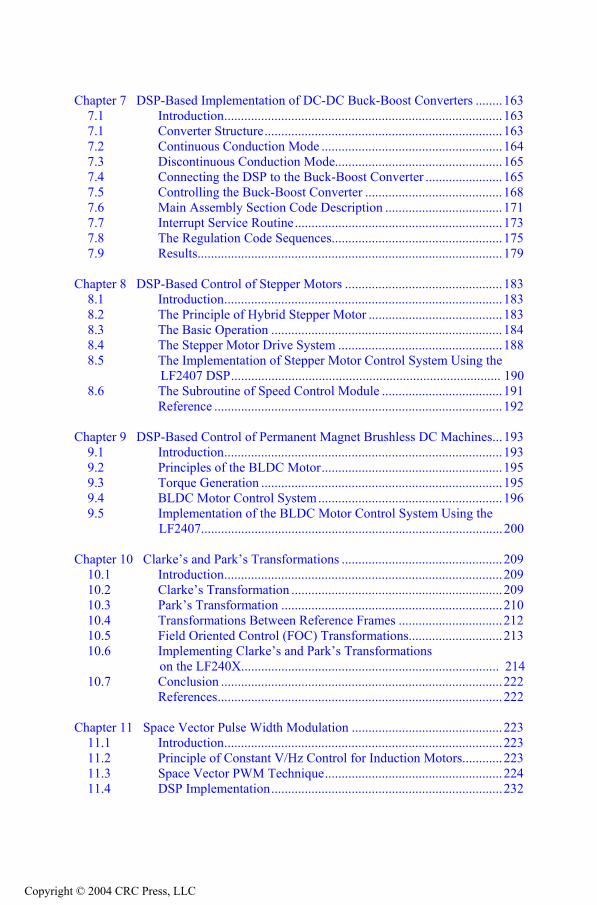
c. Click on the “Processor Configuration” tab and select the TMS320C2400 processor. Click on the “Add Single” button. You should the see “CPU_1” under the “processors on the board” list.
d. Click on the “Finish” button located at the lower right corner of the “Board
Properties” box. The setup is now complete. Go to File/Save to save the configuration. Close the Code Composer Setup window.
Now that everything is connected properly, we shall begin with the CCS
exercise:
1. Turn on the EVM. The green LED on the top right of the board will confirm that there is power to the board.
2. Open Code Composer Studio by running cc_app.exe either from the desktop icon, Start/Programs/Code Composer, or C:\tic2xx\cc\bin\cc_app.exe.
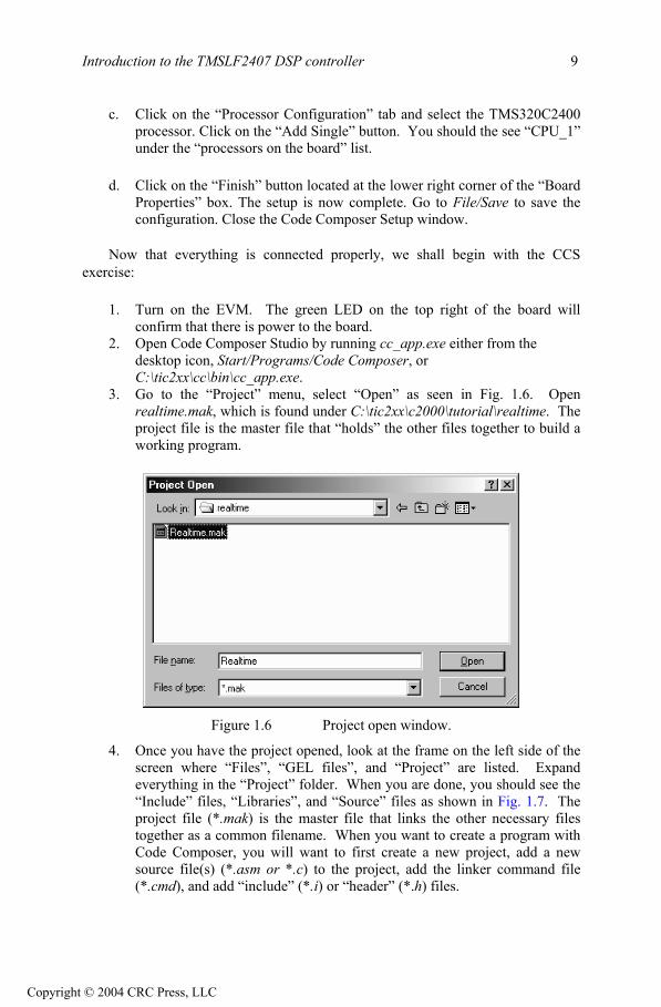
3. Go to the “Project” menu, select “Open” as seen in Fig. 1.6. Open realtime.mak, which is found under C:\tic2xx\c2000\tutorial\realtime. The project file is the master file that “holds” the other files together to build a working program.
Figure 1.6 Project open window.
4. Once you have the project opened, look at the frame on the left side of the screen where “Files”, “GEL files”, and “Project” are listed. Expand everything in the “Project” folder. When you are done, you should see the “Include” files, “Libraries”, and “Source” files as shown in Fig. 1.7. The project file (*.mak) is the master file that links the other necessary files together as a common filename. When you want to create a program with Code Composer, you will want to first create a new project, add a new source file(s) (*.asm or *.c) to the project, add the linker command file (*.cmd), and add “include” (*.i) or “header” (*.h) files.
Copyright © 2004 CRC Press, LLC

Introduction to the TMSLF2407 DSP controller 10
As in other programming languages, “include” (*.i) and “header” (*.h) files are user-defined files that are common to most programs. Functionally *.h and *.i files are the same. Both types of files can define constants, macros (user defined callable functions), or variables. In this case, we want to run our program in real-time mode. Therefore, we need a real-time monitor program (C200mntr.i in this program). The file X24x.h contains variable names for data memory mapped control registers. The code that is in the header (*.h) or include (*.i) file could be written in the actual source code, but it is easier to just make general register definitions as a header file that can be used with many projects.
The linker command file (*.cmd) is vital to the proper building of your code. It specifies where in the program memory to place sections of the program code, defines memory blocks, contains linker options, and names input files for the linker, names the (.out) etc. The linker command file also specifies memory allocations. Without a proper linker command file, CCS will not build the program properly. In this case, the linker command file is named realtime.cmd.
Source (*.c or *.asm) files contain the actual program that is to be run on the DSP. You must have at least one source file, but may have source files that call other source files. Be sure all relevant source files are added to the project.
Figure 1.7 CCS window with opened project.
Copyright © 2004 CRC Press, LLC
Introduction to the TMSLF2407 DSP controller 11
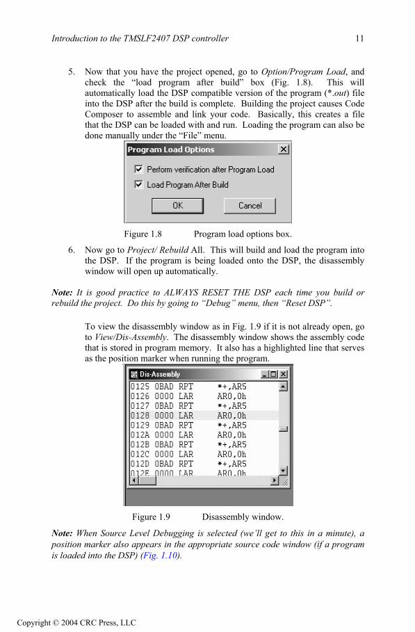
5. Now that you have the project opened, go to Option/Program Load, and check the “load program after build” box (Fig. 1.8). This will automatically load the DSP compatible version of the program (*.out) file into the DSP after the build is complete. Building the project causes Code Composer to assemble and link your code. Basically, this creates a file that the DSP can be loaded with and run. Loading the program can also be done manually under the “File” menu.
Figure 1.8 Program load options box.
6. Now go to Project/ Rebuild All. This will build and load the program into the DSP. If the program is being loaded onto the DSP, the disassembly window will open up automatically.
Note: It is good practice to ALWAYS RESET THE DSP each time you build or rebuild the project. Do this by going to “Debug” menu, then “Reset DSP”.
To view the disassembly window as in Fig. 1.9 if it is not already open, go to View/Dis-Assembly. The disassembly window shows the assembly code that is stored in program memory. It also has a highlighted line that serves as the position marker when running the program.
Figure 1.9 Disassembly window.
Note: When Source Level Debugging is selected (we’ll get to this in a minute), a position marker also appears in the appropriate source code window (if a program is loaded into the DSP) (Fig. 1.10).
Copyright © 2004 CRC Press, LLC

Introduction to the TMSLF2407 DSP controller 12
Figure 1.10 Source level debugging.
7. The CPU registers and CPU status registers are very helpful in debugging
code. To view these registers, go to View/CPU Registers (both registers are under this menu). Open both CPU registers. You should see the registers appear in new frames on the screen.
8. The ability to view memory locations is also vital to debugging. To view
memory, go to View/Memory. You should see a box pop up which will configure the memory window that is about to open (see Fig. 1.11). Enter 0x0300 for the start address.
Figure 1.11 Memory viewing window.
Copyright © 2004 CRC Press, LLC

Introduction to the TMSLF2407 DSP controller 13
You can also change the values for the CPU registers and memory locations by double clicking on the register or memory location. A box will pop up that will allow you to enter in a new value.
Double click on the 0x300 location in the memory window and change the value to 0x0555. The new value will appear in red signifying that the memory location has been changed.
Using the same technique, change a few registers in the CPU status and CPU register frames. Observe how the values in the registers change to the new value entered.
9. In MAIN.ASM scroll down until you see the line “.bss Main_counter,1”.
Highlight “Main_counter” and add that variable to the watch window.
A watch window allows us to view variables that we use in our code. Open a watch window by going to View/Watch Window. You can add variables to this window by highlighting the variable name in the source code and then right clicking the mouse button and selecting “add to watch window”. Now, let us edit the display format of this variable in the watch window. Double click on the variable name in the watch window. When the “edit variable” box appears, add the command “*(int*)” in front of the variable name (see Fig. 1.12). This configures the variable in the watch window to be displayed as an integer, thus ensuring that a decimal value is displayed. Otherwise, a hex value will be displayed.
Figure 1.12 Editing a variable while in the watch window.
10. Rebuild the project (which should load the program as well) and reset the
DSP by going to Debug Menu/Reset DSP.
Note: If a source code window opens up as well as the disassembly window when the project is built, Source Level Debugging is enabled. If not, enable Source Level Debugging by going to Project/Options/Assembler Tab and check the “enable source level debugging” (Fig. 1.13). Source level debugging lets you see where in the source code the program is running instead of having to decipher the disassembly window information. If you have just enabled Source Level Debugging, you need to rebuild the project before it takes effect.
Copyright © 2004 CRC Press, LLC

Introduction to the TMSLF2407 DSP controller 14
Figure 1.13 Build options menu box.
11. Enable Real Time mode by performing the following steps:
a. The DSP must have the program already loaded in order to enable real-time mode. (While in real-time mode, programs cannot be loaded to the DSP.)
b. Reset the DSP by going to Debug Menu / Reset DSP. c. Open the Command Window by going to Tools Menu / Command
Window. d. Type in the Command Window “go MON_GO”. e. Put CCS in Real-time mode by going to Debug Menu / Real-time
Mode. When in real-time mode, you will se the word “REALTIME” in the bottom of the code composer screen.
f. Reset the DSP again and the program is ready to RUN.
Copyright © 2004 CRC Press, LLC

Introduction to the TMSLF2407 DSP controller 15
Note: Real-time mode is a useful feature of CCS that allows you to see changes as they happen but is not necessary for program debugging. When CCS is not in real time mode, the values in all windows will update as soon as the program is halted or a break point occurs.
Right click on the watch window and choose “Continuous Refresh”. This will allow the values in the Watch window to change.
12. We are now ready to run the demonstration program. First make sure that
no breakpoints have been set or the DSP will stop when it reaches the breakpoint.
Run the program by going to Debug/Run. Running and halting the DSP can also be performed by hitting F5 to run and Shift-F5 to halt. Observe as the value of “Main_counter” in the watch window changes.
13. Halt the DSP by going to Debug/Halt. In the disassembly or source
window you should see that the program is halted somewhere in the area of code entitled “Loop” (hex address 0159-015D in the disassembly window (program memory)). Left click on a line in the “Loop” section and toggle a breakpoint by right clicking the mouse and selecting “toggle breakpoint”. You should see a purple line appear where the breakpoint is set (Fig. 1.14). Notice how the breakpoint appears in both the disassembly window and the window containing the assembly source code.
Figure 1.14 Breakpoint is located at the highlighted line (source level debug).
Copyright © 2004 CRC Press, LLC

Introduction to the TMSLF2407 DSP controller 16
14. Run the program and watch as the DSP stops at the breakpoint each time it passes through the “Loop” section. (You will need to “run” the DSP each time after it hits a breakpoint because the breakpoint essentially “pauses” the DSP.) Observe as the value of Main_counter increments by 1 in the watch window each time the code is restarted after the breakpoint. Remove the breakpoint by toggling it off.
Note: If you wish to single step through the code regardless of whether or not a breakpoint is set, you can do this by choosing Debug/Step Into or pressing F8.
15. If you wish to save the screen configuration (position of windows, what
appears on the screen, etc.) go to File Menu/Workspace/save workspace shown in Fig. 1.15.
Now, when you re-open CCS in the future, you will only have to load the workspace, saving you the trouble of opening the memory, CPU, and source code windows shown in Fig. 1.16. Saving a workspace not only saves window configuration, but project configuration as well. If a previously saved workspace is opened, the project that was open at the time of the workspace save will also open. While saving a workspace saves screen configuration, it does not save the contents of any files or the project!
Figure 1.15 Saving a workspace.
Copyright © 2004 CRC Press, LLC
Introduction to the TMSLF2407 DSP controller 17
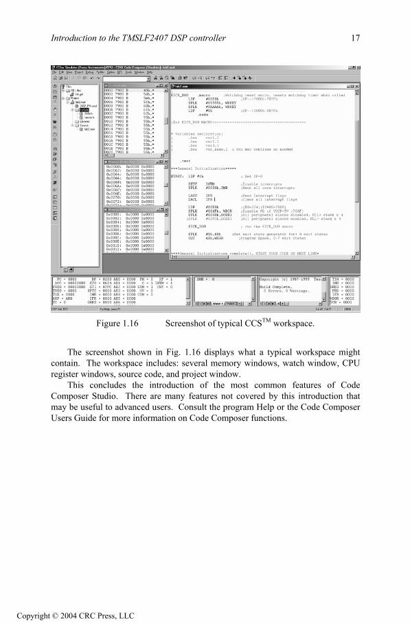
Figure 1.16 Screenshot of typical CCSTM workspace.
The screenshot shown in Fig. 1.16 displays what a typical workspace might
contain. The workspace includes: several memory windows, watch window, CPU register windows, source code, and project window.
This concludes the introduction of the most common features of Code Composer Studio. There are many features not covered by this introduction that may be useful to advanced users. Consult the program Help or the Code Composer Users Guide for more information on Code Composer functions.
Copyright © 2004 CRC Press, LLC

Chapter 2
C2xx DSP CPU AND INSTRUCTION SET
2.1 Introduction to the C2xx DSP Core and Code Generation
The heart of the LF2407 DSP Controller is the C2xx DSP core. This core is a 16-bit fixed point processor, meaning that it works with 16-bit binary numbers. One can think of the C2xx as the central processor in a personal computer. The LF2407 DSP consists of the C2xx DSP core plus many peripherals such as Event Managers, ADC, etc., all integrated onto one single chip. This chapter will discuss the C2xx DSP core, subcomponents, and instruction set.
The C2xx core has its own native instruction set of assembly mnemonics or commands. Through the use of CCS and the associated compiler, one has the freedom of writing code in both C language and the native assembly language. However, to write compact, fast executing programs, it is best to compose code in assembly language. Due to this reason, programming in assembly will be the focus of this book. However, we will also include an example of a software tool called VisSimTM, by Visual Solutions. VisSim allows users to simulate algorithms and develop code in “block” form. More on VisSim will be presented in the Appendix. 2.2 The Components of the C2xx DSP Core
The DSP core (like all microprocessors) consists of several subcomponents necessary to perform arithmetic operations on 16-bit binary numbers. The following is a list of the multiple subcomponents found in the C2xx core which we will discuss further:
• A 32-bit central arithmetic logic unit (CALU) • A 32-bit accumulator (used frequently in programs) • Input and output data-scaling shifters for the CALU • A (16-bit by 16-bit) multiplier • A product-scaling shifter • Eight auxiliary registers (AR0 – AR7) and an auxiliary register arithmetic
unit (ARAU)
Each of the above components is either accessed directly by the user code or is indirectly used during the execution of an assembly command. Central Arithmetic Logic Unit (CALU)
The C2xx performs 2s-complement arithmetic using the 32-bit CALU. The CALU uses 16-bit words taken from data memory, derived from an immediate instruction, or from the 32-bit multiplier result. In addition to arithmetic operations, the CALU can perform Boolean operations. The CALU is somewhat transparent to
19
Copyright © 2004 CRC Press, LLC

C2xx DSP CPU and Instruction Set 20
the user. For example, if an arithmetic command is used, the user only needs to write the command and later read the output from the appropriate register. In this sense, the CALU is “transparent” in that it is not accessed directly by the user. Accumulator
The accumulator stores the output from the CALU and also serves as another input to the CALU (many arithmetic commands perform operations on numbers that are currently stored in the accumulator; versus other memory locations). The accumulator is 32 bits wide and is divided into two sections, each consisting of 16 bits. The high-order bits consist of bits 31 through 16, and the low-order bits are made up of bits 15 through 0. Assembly language instructions are provided for storing the high- and low-order accumulator words to data memory. In most cases, the accumulator is written to and read from directly by the user code via assembly commands. In some instances, the accumulator is also transparent to the user (similar to the CALU operation in that it is accessed “behind the scenes”). Scaling Shifters
The C2xx has three 32-bit shifters that allow for scaling, bit extraction, extended arithmetic, and overflow-prevention operations. The scaling shifters make possible commands that shift data left or right. Like the CALU, the operation of the scaling shifters is “transparent” to the user. For example, the user needs only to use a shift command, and observe the result. Any one of the three shifters could be used by the C2xx depending on the specific instruction entered. The following is a description of the three shifters:
• Input data-scaling shifter (input shifter): This shifter left-shifts 16-bit
input data by 0 to 16 bits to align the data to the 32-bit input of the CALU. For example, when the user uses a command such as “ADD 300h, 5”, the input shifter is responsible for first shifting the data in memory address “300h” to the left by five places before it is added to the contents of the accumulator.
• Output data-scaling shifter (output shifter): This shifter left-shifts data
from the accumulator by 0 to 7 bits before the output is stored to data memory. The content of the accumulator remains unchanged. For example, when the user uses a command such as “SACL 300h, 4”, the output shifter is responsible for first shifting the contents of the accumulator to the left by four places before it is stored to the memory address “300h”.
Copyright © 2004 CRC Press, LLC

C2xx DSP CPU and Instruction Set 21
• Product-scaling shifter (product shifter): The product register (PREG) receives the output of the multiplier. The product shifter shifts the output of the PREG before that output is sent to the input of the CALU. The product shifter has four product shift modes (no shift, left shift by one bit, left shift by four bits, and right shift by six bits), which are useful for performing multiply/accumulate operations, fractional arithmetic, or justifying fractional products.
Multiplier
The multiplier performs 16-bit, 2s-complement multiplication and creates a 32-bit result. In conjunction with the multiplier, the C2xx uses the 16-bit temporary register (TREG) and the 32-bit product register (PREG).
The operation of the multiplier is not as “transparent” as the CALU or shifters. The TREG always needs to be loaded with one of the numbers that are to be multiplied. Other than this prerequisite, the multiplication commands do not require any more actions from the user code. The output of the multiply is stored in the PREG, which can later be read by the user code. Auxiliary Register Arithmetic Unit (ARAU) and Auxiliary Registers
The ARAU generates data memory addresses when an instruction uses indirect addressing to access data memory (more on indirect addressing will be covered later along with assembly programming). Eight auxiliary registers (AR0 through AR7) support the ARAU, each of which can be loaded with a 16-bit value from data memory or directly from an instruction. Each auxiliary register value can also be stored in data memory. The auxiliary registers are mainly used as “pointers” to data memory locations to more easily facilitate looping or repeating algorithms. They are directly written to by the user code and are automatically incremented or decremented by particular assembly instructions during a looping or repeating operation. The auxiliary register pointer (ARP) embedded in status register ST0 references the auxiliary register. The status registers (ST0, ST1) are core level registers where values such as the Data Page (DP) and ARP located. More on the operation and use of auxiliary registers will be covered in subsequent chapters.
2.3 Mapping External Devices to the C2xx Core and the Peripheral
Interface
Since the LF2407 contains many peripherals that need to be accessed by the C2xx core, the C2xx needs a way to read and write to the different peripherals. To make this possible, peripherals are mapped to data memory (memory will be covered shortly). Each peripheral is mapped to a corresponding block of data memory addresses. Where applicable, each corresponding block contains configuration registers, input registers, output registers, and status registers. Each peripheral is accessed by simply writing to the appropriate registers in data memory, provided the peripheral clock is enabled (see System Configuration registers).
Copyright © 2004 CRC Press, LLC

C2xx DSP CPU and Instruction Set 22
The peripherals are linked to the internal memory interface of the CPU through the PBUS interface shown in Fig. 2.1. All on-chip peripherals are accessed through the Peripheral Bus (PBUS). All peripherals, excluding the WD timer counter, are clocked by the CPU clock (which has a selectable frequency), and must be enabled via the system configuration registers.
C2xx CPU + JTAG + 544 x 16 DARAM
Mem I/F
Logic I/F
P bus I/F
I/O registers
ADC controlCAN WDSCI
ADC
P bus
Synthesized ASIC gates
Flash/ROM (up to 32K × 16)
SPI Event
Managers (EVA and EVB)
Interrupts reset, etc.
SARAM (up to 2K × 16)
Figure 2.1 Functional block diagram of the LF2407 DSP controller.
2.4 System Configuration Registers
The System Control and Status Registers (SCSR1, SCSR2) are used to configure or display fundamental settings of the LF2407. For example, these fundamental settings include the clock speed (clock pre-scale setting) of the LF2407, which peripherals are enabled, microprocessor/microcontroller mode, etc. Bits are controlled by writing to the corresponding data memory address or the logic level on an external pin as with the microprocessor/microcontroller (MP/MC) select bit. The bit descriptions of these two registers (mapped to data memory) are listed below.
System Control and Status Register 1 (SCSR1) — Address 07018h
15 14 13 12 11 10 9 8
Reserved CLKSRC LPM1 LPM0 CLK PS2 CLK PS1 CLK PS0 Reserved
R–0 RW–0 RW–0 RW–0 RW–1 RW–1 RW–1 R–0
7 6 5 4 3 2 1 0
ADC CLKEN
SCI CLKEN
SPI CLKEN
CAN CLKEN
EVB CLKEN
EVA CLKEN
Reserved ILLADR
RW–0 RW–0 RW–0 RW–0 RW–0 RW–0 R–0 RC–0 Note: R = read access, W = write access, C = clear, -0 = value after reset.
Copyright © 2004 CRC Press, LLC
C2xx DSP CPU and Instruction Set 23
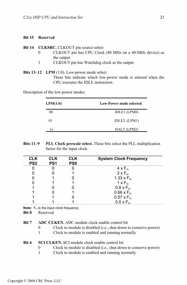
Bit 15 Reserved Bit 14 CLKSRC. CLKOUT pin source select
0 CLKOUT pin has CPU Clock (40 MHz on a 40-MHz device) as the output
1 CLKOUT pin has Watchdog clock as the output
Bits 13–12 LPM (1:0). Low-power mode select These bits indicate which low-power mode is entered when the CPU executes the IDLE instruction.
Description of the low-power modes:
LPM(1:0) Low-Power mode selected
00 IDLE1 (LPM0)
01 IDLE2. (LPM1)
1x HALT (LPM2) Bits 11–9 PLL Clock prescale select. These bits select the PLL multiplication
factor for the input clock.
CLK PS2
CLK PS1
CLK PS0
System Clock Frequency
0 0 0 4 x Fin 0 0 1 2 x Fin 0 1 0 1.33 x Fin 0 1 1 1 x Fin 1 0 0 0.8 x Fin 1 0 1 0.66 x Fin 1 1 0 0.57 x Fin 1 1 1 0.5 x Fin
Note: Fin is the input clock frequency. Bit 8 Reserved Bit 7 ADC CLKEN. ADC module clock enable control bit
0 Clock to module is disabled (i.e., shut down to conserve power) 1 Clock to module is enabled and running normally
Bit 6 SCI CLKEN. SCI module clock enable control bit
0 Clock to module is disabled (i.e., shut down to conserve power) 1 Clock to module is enabled and running normally
Copyright © 2004 CRC Press, LLC

C2xx DSP CPU and Instruction Set 24
Bit 5 SPI CLKEN. SPI module clock enable control bit
0 Clock to module is disabled (i.e., shut down to conserve power) 1 Clock to module is enabled and running normally
Bit 4 CAN CLKEN. CAN module clock enable control bit
0 Clock to module is disabled (i.e., shut down to conserve power) 1 Clock to module is enabled and running normally
Bit 3 EVB CLKEN. EVB module clock enable control bit
0 Clock to module is disabled (i.e., shut down to conserve power) 1 Clock to module is enabled and running normally
Bit 2 EVA CLKEN. EVA module clock enable control bit
0 Clock to module is disabled (i.e., shut down to conserve power) 1 Clock to module is enabled and running normally
Note: In order to modify/read the register contents of any peripheral, the clock to that peripheral must be enabled by writing a 1 to the appropriate bit. Bit 1 Reserved Bit 0 ILLADR. Illegal Address detect bit
If an illegal address has occurred, this bit will be set. It is up to software to clear this bit following an illegal address detect. This bit is cleared by writing a 1 to it and should be cleared as part of the initialization sequence. Note: An illegal address will cause a Non-Maskable Interrupt (NMI).
System Control and Status Register 2 (SCSR2) — Address 07019h
15-8
Reserved
RW–0
7 6 5 4 3 2 1 0
Reserved I/P QUAL WD OVERRIDE
XMIF HI–Z BOOT EN MP/MC DON PON
RW–0 RC–1 RW–0 RW–BOOT EN pin
RW– MP/MC pin
RW–1 RW–1
Note: R = read access, W = write access, C = clear, -0 = value after reset. Bits 15–7 Reserved. Writes have no effect; reads are undefined
Copyright © 2004 CRC Press, LLC

C2xx DSP CPU and Instruction Set 25
Bit 6 Input Qualifier Clocks. An input-qualifier circuitry qualifies the input signal to the CAP1–6, XINT1/2, ADCSOC, and PDPINTA/B pins in the 240xA devices. The I/O functions of these pins do not use the input-qualifier circuitry. The state of the internal input signal will change only after the pin is held high/low for 6 (or 12) clock edges. This ensures that a glitch smaller than (or equal to) 5 (or 11) CLKOUT cycles wide will not change the internal pin input state. The user must hold the pin high/low for 6 (or 12) cycles to ensure that the device will see the level change. This bit determines the width of the glitches (in number of internal clock cycles) that will be blocked. Note that the internal clock is not the same as CLKOUT, although its frequency is the same as CLKOUT.
0 The input-qualifier circuitry blocks glitches up to 5 clock cycles
long 1 The input-qualifier circuitry blocks glitches up to 11 clock cycles
long Note: This bit is applicable only for the 240xA devices, not for the 240x devices because they lack an input-qualifier circuitry. Bit 5 Watchdog Override. (WD protect bit)
After RESET, this bit gives the user the ability to disable the WD function through software (by setting the WDDIS bit = 1 in the WDCR). This bit is a clear-only bit and defaults to a 1 after reset.
Note: This bit is cleared by writing a 1 to it.
0 Protects the WD from being disabled by software. This bit cannot
be set to 1 by software. It is a clear-only bit, cleared by writing a 1 1 This is the default reset value and allows the user to disable the
WD through the WDDIS bit in the WDCR. Once cleared, however, this bit can no longer be set to 1 by software, thereby protecting the integrity of the WD timer
Bit 4 XMIF Hi-Z Control
This bit controls the state of the external memory interface (XMIF) signals.
0 XMIF signals in normal driven mode; i.e., not Hi-Z (high impedance)
1 All XMIF signals are forced to Hi-Z state
Copyright © 2004 CRC Press, LLC

C2xx DSP CPU and Instruction Set 26
Bit 3 Boot Enable This bit reflects the state of the BOOT_EN / XF pin at the time of reset. After reset and device has “booted up”, this bit can be changed in software to re-enable Flash memory visibility or return to active Boot ROM.
0 Enable Boot ROM — Address space 0000 — 00FF is now occupied by the on-chip Boot ROM Block. Flash memory is totally disabled in this mode. Note: There is no on-chip boot ROM in ROM devices (i.e., LC240xA)
1 Disable Boot ROM — Program address space 0000 — 7FFF is mapped to on-chip Flash memory in the case of LF2407A and LF2406A. In the case of LF2402A, addresses 0000 – 1FFF are mapped
Bit 2 Microprocessor/Microcontroller Select
This bit reflects the state of the MP/MC pin at time of reset. After reset, this bit can be changed in software to allow dynamic mapping of memory on and off chip.
0 Set to Microcontroller mode — Program Address range 0000 — 7FFF is mapped internally (i.e., Flash)
1 Set to Microprocessor mode — Program Address range 0000 — 7FFF is mapped externally (i.e., customer provides external memory device.)
Bits 1–0 SARAM Program/Data Space Select
DON PON SARAM status 0 0 SARAM not mapped (disabled), address space allocated to
external memory 0 1 SARAM mapped internally to Program space 1 0 SARAM mapped internally to Data space 1 1 SARAM block mapped internally to both Data and
Program spaces. This is the default or reset value
Note: See memory map for location of SARAM addresses
2.5 Memory
Memory is required to hold programs, perform operations, and execute programming instructions. There are three main blocks of memory which are present on the LF2407 chip: B0, B1, and B2. Additionally, there are two different memory “spaces” (program, data) in which blocks are used. We will discuss exactly what each memory “block” and memory “space” is, and what each is used for.
Copyright © 2004 CRC Press, LLC

C2xx DSP CPU and Instruction Set 27
2.5.1 Memory Blocks and Types
A block of memory on the LF2407 is simply a specified range of memory addresses (each address consists of a 16-bit word of memory). There are three main memory blocks on the LF2407 that can be specified via the Linker Command File (we will discuss the Linker Command File and other files types when we cover programming).
The LF2407 has 544 16-bit words of on-chip Double Access Random Access Memory (DARAM) that are divided into three main memory blocks named B0, B1, and B2. In addition to the DARAM, there are also 2000 16-bit words of Single Access Random Access Memory (SARAM). The main difference between DARAM and SARAM is that DARAM memory can be accessed twice per clock cycle and SARAM can only be accessed once per cycle. Thus, DARAM reads and writes twice as fast as SARAM.
In addition to the RAM present on the LF2407, there is also non-volatile Flash memory. Unlike RAM, the Flash memory does not lose its contents when the LF2407 loses power. Flash memory can only be written to by “flashing” the memory, which is a process that can only be done manually by a user. Therefore, Flash memory on the LF2407 is used only to store a program that is to be run. As stated in Chapter 1, it is only necessary to use the Flash memory if the DSP is to be run independently from a PC and JTAG interface. Though we introduce Flash memory, it will not be covered in this text. However, the reader is encouraged to consult the Texas Instruments documentation on Flash memory. Flash memory can prove to be a valuable code development tool when it comes time to test a LF2407 program where having a PC connected is impractical.
2.5.2 Memory Space and Allocation
There are two ways of using the physical memory on board the LF2407: storing a program or storing data.
A program that is to be run must be stored in memory that is mapped to program space. Likewise, only memory that is in data space may be used to store data. Program memory is written to when a program is loaded into the LF2407. Data memory is normally written to during the execution of a program, where the program might use the data memory as temporary storage for calculation variables and results.
Memory blocks B1 and B2 are configured as data memory. The B0 block is primarily intended to hold data, but can be configured to act as either program or data memory, depending on the value of the CNF bit in Status Register ST1. CNF = 0 maps B0 in data memory, while CNF = 1 maps B0 in program memory.
The memory addresses associated with the SARAM can be configured for both data memory and program memory, and are also software configurable to either
Copyright © 2004 CRC Press, LLC

C2xx DSP CPU and Instruction Set 28
access external memory or the internal SARAM. When configured for internal, the SARAM can be used as data or program memory. However, when configured as external, these addresses are used for off-chip program memory. SARAM is useful if more memory is needed for data than the B0, B1, and B2 blocks can provide. The SARAM addresses should be configured to either program or data space via the Linker Command File.
The on-chip flash in the LF2407 is mapped to program memory space when the external MP/MC-pin is pulled low. When the MP/MC-pin is pulled high, the program memory is mapped to external memory addresses, access via memory that is physically external to the LF2407. In the case of the Spectrum Digital EVM, external memory is installed on the board and a jumper pulls the MP/MC pin high or low.
2.5.3 Memory Maps
Program Memory
When a program is loaded into the LF2407, the code resides in and is run from program memory space. In addition to storing the user code, the program memory can also store immediate operands and table information. Figure 2.2 shows the various program memory addresses (in hexadecimal) and how they are used.
0000h
003Fh 0040h
FDFFh FE00h
FFFFh
0000h-0001h 0002h-0003h 0004h-0005h 0006h-0007h 0008h-0009h 000Ah-000Bh 000Ch-000Dh 000Eh-000Fh
0022h-0023h 0024h-0025h
External
Reset
Interrupt level 1
Interrupt level 2
Interrupt level 3
Interrupt level 4
Interrupt level 5
Interrupt level 6
TRAP
NMI
0010h-0021h Software interrupts
Reserved
Reserved 0026h-0027h
7FFFh 8000h
On-chip FEFFh FF00h
DARAM (B0) (CNF = 1)
(External if CNF = 0)
32K on-chip flash (MP/MC = 0)External (MP/MC = 1)
Software interrupts 0028h-003Fh
Reserved (CNF = 1)
(External if CNF = 0)
User code in flash memory
Interrupt vectors
Code security passwords0043h 0044h
Figure 2.2 Program memory map for LF2407. (Courtesy of Texas Instruments)
Copyright © 2004 CRC Press, LLC

C2xx DSP CPU and Instruction Set 29
Two factors determine the configuration of program memory:
CNF bit: The CNF bit determines if B0 memory is in on-chip program space: CNF = 0. The 256 words are mapped as external memory. CNF = 1. The 256 words of DARAM B0 are configured for program use.
At reset, B0 is mapped to data space (CNF = 0). MP/MC pin:
The level on the MP/MC pin determines if program instructions are read from on-chip Flash/ROM or external memory:
MP/MC = 0. The device is configured in microcontroller mode. The on-chip flash EEPROM is accessible. The device fetches the reset vector from on-chip memory.
MP/MC = 1. The device is configured in microprocessor mode. Program
memory is mapped to external memory.
Data Memory
For the execution of a program, it is necessary to store calculation results or look up tables in memory. The memory allocated for this function is called data memory. In order to store a value to a data memory address (dma), the corresponding memory block must reside in data memory space. Blocks B1 and B2 discussed earlier permanently reside in data space, while block B0 and the SARAM are configurable for either program or data.
Data memory space has the second functionality of providing an easy way to access on-chip configuration registers and peripherals. Each user configurable peripheral has associated registers in data memory addresses that may be written to or read from as needed. For example, the control registers for the analog-to-digital converter (ADC) are each located in the data memory range of 70A0h to 70BFh. The internal data memory includes the memory-mapped registers, DARAM blocks, and peripheral memory-mapped registers. The remaining 32K words of memory (8000h to FFFFh) form part of the external data memory.
Copyright © 2004 CRC Press, LLC

C2xx DSP CPU and Instruction Set 30
Reserved
Reserved
Reserved
70C0-70FF
General-purpose timer registers
flag registersInterrupt mask, vector, and
Event manager - EVB
deadband registersCompare, PWM, and
Capture and QEP registers
7500-7508 7511-7519 7520-7529 752C-7531 7532-753F
7432-743F 742C-7431 7420-7429 7411-7419 7400-7408
Illegal
Event manager - EVA
710F-71FF 7100-710E
70A0-70BF 7090-709F 7080-708F 7070-707F 7060-706F 7050-705F 7040-704F 7030-703F 7020-702F 7010-701F 7000-700F
CAN control registers
ADC control registers
Digital I/O control registers
External-interrupt registers
SCI
SPI
Watchdog timer registers
control registersSystem configuration and
Hex Hex
005F 0007 0006 0005 0004 0003 0000
and reservedEmulation registers
Interrupt flag register
Interrupt-mask register
FFFF
77F0 77EF 7540 753F 7500 74FF 7440 743F 7400 73FF 7000 6FFF 1000
07FF
0400 03FF 0300 02FF
0200 01FF
0080 007F 0060 005F
0000
External *
Peripheral frame 3 (PF3)
Peripheral frame 2 (PF2)
Peripheral frame 1 (PF1)
On-chip DARAM B1
On-chip DARAM B0
Reserved
On-chip DARAM B2
and reservedMemory-mapped registers
Indicates that access to these addresses causes a nonmaskable in-terrupt (NMI).
Reserved Indicates addresses that are re-served for test.
* Available in LF2407A only
Illegal
Illegal
Illegal
Illegal
Illegal
Illegal
Illegal
Illegal
Illegal
Illegal
Illegal
0100 00FF
Reserved
Illegal0500 04FF
SARAM (2K)0800 0FFF
CAN mailbox
Illegal 7230-73FF 7200-722F
Reserved
Code security passwords
Illegal
77F3
7800 7FFF 8000
General-purpose timer registers
flag registersInterrupt mask, vector, and
deadband registersCompare, PWM, and
Capture and QEP registers
77F4 77FF
Figure 2.3 Data memory map for the LF2407. (Courtesy of Texas Instruments)
Copyright © 2004 CRC Press, LLC

C2xx DSP CPU and Instruction Set 31
Input/Output (I/O) Space
I/O space is solely used for accessing external peripherals such as the digital-to-analog converter (DAC) on the LF2407 EVM. It is not to be confused with the I/O functionality of pins. The assembly instruction “OUT” is used to write to an address that is mapped to I/O space. Figure 2.4 depicts the basic memory map of the I/O space on the LF2407.
Wait-state generator control register*
0000h
External
FEFFFF00
FFFF
FF0E
FF0F
FF10
FFFE
Reserved
Reserved
Flash control mode register*
Figure 2.4 Memory map of I/O space. (Courtesy of Texas Instruments)
Within program, data, and I/O space are addresses that are reserved for system
functionality and may not be written to. It is important that the user pay attention to what memory ranges are used by the program and where the program is to be loaded. It is important to make sure the Linker Command File is configured properly and the correct Data Page (DP) is set to avoid inadvertently writing to an undesired or reserved memory address.
Detailed information on the memory map is given in the Texas Instruments TMS320LF/LC240xA DSP Controllers Reference Guide - System and Peripherals; Literature Number: SPRU357A.
2.6 Memory Addressing Modes
There are three basic memory addressing modes used by the C2xx instruction set. The three modes are:
• Immediate addressing mode (does not actually access memory) • Direct addressing mode • Indirect addressing mode
Copyright © 2004 CRC Press, LLC

C2xx DSP CPU and Instruction Set 32
2.6.1 Immediate Addressing Mode
In the immediate addressing mode, the instruction contains a constant to be manipulated by the instruction. Even though the name “immediate addressing” suggests that a memory location is accessed, immediate addressing is simply dealing with a user-specified constant which is usually included in the assembly command syntax. The “#” sign indicates that the value is an immediate address (just a constant). The two types of immediate addressing modes are: Short-immediate addressing. The instructions that use short-immediate addressing have an 8-bit, 9-bit, or 13-bit constant as the operand.
For example, the instruction: LACL #44h ;loads lower bits of accumulator with
;eight-bit constant (44h in this case)
Note: The LACL command will work only with a short 8-bit constant. If you want to load a long 16-bit constant, then use the LACC command.
Long-immediate addressing. Instructions that use long-immediate addressing have a 16-bit constant as an operand. This 16-bit value can be used as an absolute constant or as a 2s-complement value.
For example, the instruction:
LACC #4444h ;loads accumulator with up to a 16-bit
;constant (4444h in this case)
If you need to use registers or access locations in data memory, you must use
either direct or indirect addressing.
2.6.2 Direct Addressing Mode
In direct addressing, data memory is first addressed in blocks of 128 words called data pages. The entire 64K of data memory consists of 512 DPs labeled 0 through 511, as shown in the Fig. 2.5. The current DP is determined by the value in the 9-bit DP pointer in status register ST0. For example, if the DP value is “0 0000 0000”, the current DP is 0. If the DP value is “0 0000 0010”, the current data page is 2. The DP of a particular memory address can be found easily by dividing the address (in hexadecimal) by 80h. For example:
For the data memory address 0300h, 300h/80h = 6h so the DP pointer is 6h. Likewise, the DP pointer for 200h is 4h.
Copyright © 2004 CRC Press, LLC

C2xx DSP CPU and Instruction Set 33
1111 1111 1
0000 0000 1
0000 0001 0
0000 0001 0
0000 0000 0
Data Memory
Page 0: 0000h-007Fh
Page 1: 0080h-00FFh
Page 2: 0100h-017Fh
Page 511: FF80h-FFFFh
.
000 0000
OffsetDP Value
0000 0000 0
111 11110000 0000 1
1111 1111 1
000 0000
111 1111
000 0000
111 1111
000 0000
111 1111
.
.
.
.
.
.
.
.
.
.
.
.
.
.
.
.
.
.
..
.
..
.
..
. ...
..
.
..
.
..
. ...
Figure 2.5 Data pages and corresponding memory ranges. (Courtesy of Texas
Instruments)
In addition to the DP, the DSP must know the particular word being referenced
on that page. This is determined by a 7-bit offset. The 7-bit offset is simply the 7 least significant bits (LSBs) of the memory address. The DP and the offset make up the 16-bit memory address (see Fig. 2.6).
7 LSBs from IR
16-bit data-memory address
All 9 bits from DP
Data page pointer (DP)
Page (9 MSBs) Offset (7 LSBs)
Instruction register (IR)
8 MSBs 7 LSBs9 bits 0
Figure 2.6 Data page and offset make up a 16-bit memory address.
When you use direct addressing, the processor uses the 9 DP bits and the 7 LSBs of the instruction to obtain the true memory address. The following steps should be followed when using direct addressing:
Copyright © 2004 CRC Press, LLC

C2xx DSP CPU and Instruction Set 34
1. Set the DP. Load the appropriate value (from 0 to 511 in decimal or 0-1FF in hex) into the DP. The easiest way to do this is with the LDP instruction. The LDP instruction loads the DP directly to the ST0 register without affecting any other bits of the ST0.
LDP #0E1h ;sets the data page pointer to E1h
or LDP #225 ;sets the data page pointer to 225 decimal
;which is E1 in hexadecimal
2. Specify the offset. For example, if you want the ADD instruction to use the
value at the second address of the current data page, you would write: ADD 1h
If the data page points to 300h, then the above instruction will add the contents
of 301h to the accumulator Note: You do not have to set the data page prior to every instruction that uses direct addressing. If all the instructions in a block of code access the same data page, you can simply load the DP before the block. However, if various data pages are being accessed throughout the block of code, be sure the DP is changed accordingly.
2.6.3 Indirect Addressing Mode
Indirect addressing is a powerful way of addressing data memory. Indirect addressing mode is not dependent on the current data page as is direct addressing. Instead, when using indirect addressing you load the memory space that you would like to access into one of the auxiliary registers (ARx). The current auxiliary register acts as a pointer that points to a specific memory address.
The register pointed to by the ARP is referred to as the current auxiliary register or current AR. To select a specific auxiliary register, load the 3-bit auxiliary register pointer (ARP) with a value from 0 to 7. The ARP can be loaded with the MAR instruction or by the LARP instruction. An ARP value can also be loaded by using the ARx operand after any instruction that supports indirect addressing as seen below.
Example of using MAR:
ADD * , AR1 ;Adds using current * , then makes AR1 the
;new current AR for future uses
Example of using LARP
LARP #2 ;this will make AR2 the current AR
The C2xx provides four types of indirect addressing options:
Copyright © 2004 CRC Press, LLC

C2xx DSP CPU and Instruction Set 35
• No increment or decrement. The instruction uses the content of the current auxiliary register as the data memory address but neither increments nor decrements the content of the current auxiliary register.
• Increment or decrement by 1. The instruction uses the content of the current auxiliary register as the data memory address and then increments or decrements the content of the current auxiliary register by one.
• Increment or decrement by an index amount. The value in AR0 is the
index amount. The instruction uses the content of the current auxiliary register as the data memory address and then increments or decrements the content of the current auxiliary register by the index amount.
• Increment or decrement by an index amount using reverse carry. The
value in AR0 is the index amount. After the instruction uses the content of the current auxiliary register as the data memory address, that content is incremented or decremented by the index amount. The addition and subtraction process is accomplished with the carry propagation reversed and is useful in fast Fourier transforms algorithms.
Table 2.1 displays the various operands that are available for use with instructions while using indirect addressing mode.
Table 2.1 Indirect addressing operands.
Operand Option Example
* No increment or decrement LT * loads the temporary register TREG with the content of the data memory address referenced by the current AR.
*+ Increment by 1 LT *+ loads the TREG with the content of the data memory address referenced by the current AR and then adds 1 to the content of the current AR.
*- Decrement by 1 LT *- loads the TREG with the content of the data memory address referenced by the current AR and then subtracts 1 from the content of the current AR.
*0+ Increment by index amount LT *0+ loads the TREG with the content of the data memory address referenced by the current AR and then adds the content of AR0 to the content of the current AR.
*0- Decrement by index amount LT *0- loads the TREG with the content of the data memory address referenced by the current AR and then subtracts the content of AR0 from the content of the current AR.
*BR0+ Increment by index amount, adding with reverse carry
LT *BR0+ loads the TREG with the content of the data memory address referenced by the current AR and then adds the content of AR0 to the content of the current AR, adding with reverse carry propagation.
*BR0- Decrement by index amount, subtracting with reverse carry
LT *BR0- loads the TREG with the content of the data memory address referenced by the current AR and then subtracts the content of AR0 from the content of the current AR, subtracting with bit reverse carry propagation.
Copyright © 2004 CRC Press, LLC

C2xx DSP CPU and Instruction Set 36
2.7 Assembly Programming Using the C2xx DSP Instruction Set
This section is dedicated to developing code using the C2xx assembly instruction set and Code Composer Studio (CCS). We will start by introducing the basics of using the instruction set and provide examples of different options when using an assembly instruction. Then we will cover code development in CCS including an explanation of the main file types used to create and compile a working assembly program. Finally, an exercise will be presented to allow the reader to practice the new skills presented in this chapter.
2.7.1 Using the Assembly Instruction Set
The complete detailed instruction set for the C2xx DSP core can be found in the Texas Instruments TMS320F/C24x DSP Controllers Reference Guide: CPU and Instruction Set; Literature Number: SPRU160C. This reference guide contains a complete descriptive listing on syntax, operands, binary opcode, instruction execution order, status bits affected by the instruction, number of memory words required to store the instruction, and clock-cycles used by the instruction. The Texas Instruments documentation on the assembly instruction set is very well written. Each assembly instruction has a complete explanation of the instruction, all optional operands, and several examples of the instructions used. Since including the instruction set and complete documentation would make this book excessively long, we will assume the reader has access to the documentation referred to above.
We will therefore focus on developing code, not the instruction set itself. Each command starts with the basic assembly instruction. Each command supports specific addressing modes and options. For example, the ADD command will work with direct, indirect, and immediate addressing. In addition to the basic command, many instructions have additional options that may be used with the instruction. For example, the ADD command supports left shifting of the data before it is added to the accumulator.
The following is the instruction syntax for the ADD command:
ADD dma [, shift] ; Direct addressing
ADD dma, 16 ; Direct with left shift of 16 ADD ind [, shift [, ARn]] ; Indirect addressing ADD ind, 16 [, ARn] ; Indirect with left shift of 16
ADD #k ; Short immediate addressing ADD #lk [, shift] ; Long immediate addressing
The following is a list of the various notations used in C2xx syntax examples:
Italics Italic symbols in instruction syntax represent variables.
Copyright © 2004 CRC Press, LLC

C2xx DSP CPU and Instruction Set 37
Example: LACC dma , you can use several way to address the dma (data memory address).
LACC *
or LACC 200h
or LACC v ; where “v” is any variable assigned to data
memory
where *, 200h, and v are the data memory addresses
Boldface Characters Boldface characters must be included in the syntax.
Example: LAR dma, 16 ; direct addressing with left shift of 16
LAR AR1, 60h, 16 ; load auxiliary AR1 register with the
memory contents of 60h that was left shifted
16 bits
Example: LACC dma, [shift] ; optional left shift from 0, 15 ; defaults to 0
LACC main_counter, 8 ; shifts contents of the variable
“main_counter” data 8 places to the left
before loading accumulator
[ ] An optional operand may be placed in the placed here.
Example: LACC ind [, shift [, AR n]_] Indirect addressing
LACC * ;load Accum. w/contents of the memory
;location pointed to by the current AR.
LACC * ,5 ;load Accum. with the contents of the memory
;location pointed to by the current AR after
;the memory contents are left shifted by 5
;bits .
LACC * ,0, AR3 ;load Accum. with the contents of the memory
;location pointed to by the current AR after
;the memory contents are left shifted by 5
;bits . Now you have the option of choosing
;a new AR. In this case, AR3 will become the
;new AR.
[, x1 [, x2]] Operands x1 and x2 are optional, but you cannot
include x2 without also including x1.
Copyright © 2004 CRC Press, LLC

C2xx DSP CPU and Instruction Set 38
It is optional when using indirect addressing to modify the data. Once you supply a left shift value from 0…15 (even a shift of 0), then you have the option of changing to a new current auxiliary register (AR).
# The # sign is prefix that signifies that the number used is a constant as
opposed to memory location. Example: RPT #15 ; this syntax is using short immediate addressing. It
will repeat the next instruction 15+1 times.
LACC #60h ;this will load the accumulator with the
;constant 60h
LACC 60h ;However, this instruction will load the ;accumulator with the contents in the data
;memory location 60h, not the constant #60h
We will now provide a few examples of using the instruction set. Example 2.1
performs a few arithmetic functions with the DSP core and illustrates the nature of assembly programming. Programming with the assembly instruction set is somewhat different than languages such as C. In a high-level language, to add two numbers we might just code “c = a + b”. In assembly, the user must be sure to code everything that needs to happen in order for a task to be executed. Take the following example:
Example 2.1 - Add the two numbers “2” and “3”:
LDP #6h ;loads the proper DP for dma 300h
SPLK #2, 300h ;store the number “2” in memory address 300h
LACL #3 ;load the accumulator with the number “3”
ADD 300h ;adds contents of 300h (“2”) to the contents
;of the accumulator(“3”); accumulator = 5
Another way: LDP #6h ;loads the proper DP for dma 300h
SPLK #2h, 300h ;store the number “2h” in memory address
;300h
SPLK #3h, 301h ;stores the number “3h” into memory address
;301h
LACL 300h ;load the accumulator with the contents in
;memory location 300h
ADD 301h ;adds contents of memory address 301h (“3h”)
;to the contents of the accumulator (“2h”)
;accumulator = 5h
Looping algorithms are very common in all programming languages. In high-
level languages, the “For” and “While” loops can be used. However, in assembly, we need a slightly different approach to perform a repeating algorithm. The
Copyright © 2004 CRC Press, LLC

C2xx DSP CPU and Instruction Set 39
following example is an algorithm that stores the value “1” to memory locations 300h, 301h, 302h, 303h, and 304h.
Example 2.2- Looping Algorithm Using the Auxiliary Register LAR AR0, #4 ;load auxiliary register 0 with #4
LAR AR1, #300h ;this AR will be used as a memory pointer
LACL #1h ;loads “1” into the accumulator
LOOPER MAR *, AR1 ;makes AR1 the next current AR
SACL *+, AR0 ;writes contents of accumulator to address
;pointed to by AR1, the “+” increments AR1
;by 1, next current AR is AR0
BANZ LOOPER ;branch to LOOPER while current AR is not 0
;decrements current AR by 1 and branches
;back to LOOPER
One might wonder if assembly language is so tedious to use, why not just
program in a high-level language all the time. When code written in a high level language is compiled into assembly, the length of the code increases substantially. For example, if an assembly program takes up 50 lines, the same program written in C might take 150 lines after it is compiled. For this reason, code written in assembly almost always executed faster and uses less memory than high-level language code.
2.7.2 Code Generation in Code Composer Studio (CCS)
In order to develop a working program in CCS, one needs to understand the main file types and structure of the code composer project file. The project file (*.mak) is the main file that links the other necessary sub-files together. The sub-files mentioned include source files (*.asm for assembly), header (*.h) files, include (*.i) files, and linker command files (*.cmd).
During the “building” of a project, CCS “assembles” and “links” the source file(s) and creates a DSP compatible (*.out) file that will ultimately be loaded onto the DSP. The out file contains the user program and also information as to where in program memory it will be placed. We will start the explanation of files with the assembly source file.
The assembly source file contains the code that will be executed when the DSP program runs. While there may be many source files in large projects, it is really only necessary to have one source file. If many source files exist, the linking order must be specified in CCS in order to ensure that the code will be operational. The file that follows is template.asm. This template source file encompasses the basics of a source file. The file template.asm contains many lines of assembly instructions which include comments to explain their function.
Copyright © 2004 CRC Press, LLC

C2xx DSP CPU and Instruction Set 40
The Assembly Source File
Important Note: Only a comment ”;” or ” *” or label such as “KICK_DOG” may be written starting on the first space of a line. ALL assembly commands must start at least from the second space on a line! ;* Source File “template.asm” for 2407 DSP programs * ;* Target Hardware: 2407 DSP EVM *
. include 240x.h ;this is the register definition file, MUST
;INCLUDE!!
. include vector.h ;this is the interrupt vector file that you
;must include ;if you are using interrupts,
;if you are not using any interrupts, it
;doesn't hurt to include it anyway ;------------------------------------------------------------- ; M A C R O - Definition ;-------------------------------------------------------------
KICK_DOG .macro ;Watchdog reset macro, resets watchdog
LDP #00E0h ;DP-->7000h-707Fh
SPLK #05555h, WDKEY
SPLK #0AAAAh, WDKEY
LDP #0h ;DP-->0000h-007Fh
.endm ;********END KICK_DOG MACRO*** continued…….. continued from above ………… ;* Variables declaration: these are commented out, and are not needed unless you want to define a variable ; .bss var1,1 ; .bss var2,1 ; .bss var3,1 ; .bss var_name,1 ;you may continue as needed .text ; this is the start of the actual program ;***General Initialization*****
START: LDP #0h ;Set DP=0
SETC INTM ;Disable interrupts
SPLK #0000h, IMR ;Mask all core interrupts
LACC IFR ;Read Interrupt flags
SACL IFR ;Clear all interrupt flags
LDP #00E0h ;(E0=224)(E0*80=7000)
SPLK #006Fh, WDCR ;Disable WD if VCCP=5V (706F)
SPLK #0000h, SCSR1 ;All peripheral clocks disabled,
;PLL= clock x 4
SPLK #00FCh, SCSR1 ;All peripheral clocks enabled, PLL
;= clock x 4
KICK_DOG ; run the KICK_DOG macro
SPLK #0h, 60h ;Set wait state generator for: 0 wait states
Copyright © 2004 CRC Press, LLC

C2xx DSP CPU and Instruction Set 41
OUT 60h, WSGR ;Program Space, 0-7 wait states ;***General Initialization complete!!, START YOUR CODE ON NEXT LINE*** ;****END YOUR CODE HERE, if interrupts are used, add interrupt service ;routine under GISRx, if no interrupts are used, leave following code ;as is ******
PHANTOM KICK_DOG ;This dummy loop is just in case a wild
B PHANTOM ;interrupt happens, all non-used interrupts
;are set to branch to PHANTOM, this
;routine just resets the watchdog timer.
GISR1: RET ;Interrupt #1 service routine
GISR2: RET ;Interrupt #2 service routine
GISR3: RET ;Interrupt #3 service routine
GISR4: RET ;Interrupt #4 service routine
GISR5: RET ;Interrupt #5 service routine
GISR6: RET ;Interrupt #6 service routine
.end ;this tells the assembler that this is the
;end of the program, YOU MUST INCLUDE the
;".end"
Starting at the top of the file, we can see the comments indicated by the “*” or “;”s. Some versions of CCS might not recognize “*” as a comment indicator. Further down, the “.include” command tells CCS what header files will be included in the assembling of the project. We will discuss the purpose of header files shortly. After the header files, we see the KICK_DOG macro. The KICK_DOG macro is a subroutine that will run every time the line “KICK_DOG” is written. Basically, KICK_DOG resets the watchdog timer on the LF2407. The watchdog timer, fed by the system clock, counts up and will generate a general system reset if it reaches an overflow. This ensures that if some event (software error) causes an inadvertent system lock-up, then the DSP will be reset automatically. The basic idea is that after the lock-up subsequent reset by the watchdog, the DSP will reinitialize itself and start to function normally, thereby increasing system integrity (if the same event does not occur again!). For our learning purposes, we will disable the watchdog timer.
After the KICK_DOG macro declaration, we see an optional variable declaration section. The “.bss” command can be used to define variables, of which the values will be stored in sequential order in the memory locations specified by the “.bss” section in the linker command file. It is still necessary to set the data page for the corresponding memory address when using a variable.
The “.text” line signifies the start of the program. This is followed by the “START” label. Labels are the only syntax that may be placed on the first space of any line. The next lines initialize the LF2407, disable the watchdog timer, and set for zero wait states. Wait states introduce a delay into the external memory interface for accessing slow external memory, but are not needed for our purposes.
Copyright © 2004 CRC Press, LLC

C2xx DSP CPU and Instruction Set 42
After these instructions are written, the functional part of the user code can be considered.
Finally, we come to the interrupt vectors GISR1, GISR2, etc. The operation of interrupts will be explained in Chapter 5. Because no interrupts are currently being used, the interrupt vectors simply are set so that any hypothetical random interrupt will cause the DSP to return to the program and do nothing. We must include the (GISR1, GISR2,…) labels because they are referenced in the vector.h header file.
Header Files
Header files (*.h) like 240x.h and vector.h (both below) discussed previously serve the purpose of providing definitions or other information that would otherwise add a substantial amount of code lines to the source file. Although it is not absolutely necessary to include a header file in the source file, header files allow the user to avoid re-writing commonly used definitions from program to program. The information contained in the file 240x.h consists of setting variables in the name of actual registers to their respective data memory addresses. This allows the programmer to simply type the name of the intended control register rather than having to constantly look up the actual memory.
For example, the SCSR1 register is located at 7018h in data memory. In the file 240x.h you can see how register names are set as variables with the memory address as the value. The purpose for this is to provide for more user-friendly programming. Instead of coding:
SPLK #00FCh, 7018h ;which would work just fine for writing
;FCh to 7018h (the SCSR1 register)
we may write:
SPLK #00FCh, SCSR1 ;not only is this easier, but it aids in
;documentation as well
The file “240x.h” contains the control register definitions. A section of the file is included below: ;********************************************************************* ; File name: 240x.h ; Description:240x register definitions, Bit codes for BIT instruction ;********************************************************************* ; 240x CPU core registers IMR .set 0004h ; Interrupt Mask Register
IFR .set 0006h ; Interrupt Flag Register
; System configuration and interrupt registers
SCSR1 .set 7018h ; System Control & Status register. 1
SCSR2 .set 7019h ; System Control & Status register. 2
Copyright © 2004 CRC Press, LLC

C2xx DSP CPU and Instruction Set 43
DINR .set 701Ch ; Device Identification Number register.
PIVR .set 701Eh ; Peripheral Interrupt Vector register.
PIRQR0 .set 7010h ; Peripheral Interrupt Request register 0
PIRQR1 .set 7011h ; Peripheral Interrupt Request register 1
PIRQR2 .set 7012h ; Peripheral Interrupt Request register 2
.
.
The header file vector.h contains interrupt vector information. This file
specifies what section of source code the processor will branch to when an interrupt occurs. By looking at the file, we can see that we have many branch statements. When an interrupt occurs, the processor first branches to 0h in program memory. It then sequentially checks each program memory address for an identifiable interrupt label (INTx) that corresponds to the pending interrupt. When it finds a match, it executes the instruction on that line, which in this case is a “B GISRx” instruction. The branch instruction causes the DSP to branch to the GISRx label (which is in the source code) under which the interrupt service routine is written. The processor then starts executing the code under that section.
INT1 through INT6 are the corresponding labels for these interrupts in the vector file. Notice the “B GISRx” command after each “INTx”. More on interrupts will be covered later in Chapter 5.
The file “vector.h” contains the interrupt vectors for the LF2407. A section of this file is shown below: ;******************************************************************* ; File name: vector.h ; Interrupt Vector declarations ; This section contains the vectors for various interrupts in the ; 240x. Unused interrupts are shown to branch to a "phantom" interrupt ; service routine which loops to itself. Users should replace the ; label PHANTOM with the label of their interrupt subroutines in case ; these interrupts are used. ;******************************************************************* .sect "vectors"
RSVECT B START ; Reset Vector
INT1 B GISR1 ; Interrupt Level 1
INT2 B GISR2 ; Interrupt Level 2
INT3 B GISR3 ; Interrupt Level 3
INT4 B GISR4 ; Interrupt Level 4
INT5 B GISR5 ; Interrupt Level 5
INT6 B GISR6 ; Interrupt Level 6
RESERVED B PHANTOM ; Reserved
SW_INT8 B PHANTOM ; Software Interrupt
SW_INT9 B PHANTOM ; Software Interrupt
SW_INT10 B PHANTOM ; Software Interrupt
Copyright © 2004 CRC Press, LLC

C2xx DSP CPU and Instruction Set 44
SW_INT11 B PHANTOM ; Software Interrupt
SW_INT12 B PHANTOM ; Software Interrupt
SW_INT13 B PHANTOM ; Software Interrupt
SW_INT14 B PHANTOM ; Software Interrupt
SW_INT15 B PHANTOM ; Software Interrupt
SW_INT16 B PHANTOM ; Software Interrupt
TRAP B PHANTOM ; Trap vector
NMI B NMI ; Non-maskable Interrupt
EMU_TRAP B PHANTOM ; Emulator Trap
SW_INT20 B PHANTOM ; Software Interrupt
SW_INT21 B PHANTOM ; Software Interrupt
SW_INT22 B PHANTOM ; Software Interrupt
.
.
The linker command file (*.cmd) specifies to CCS where valid memory exists
in both program and data memory. It also specifies where the .text, .sect, .bss, and other sections will be placed in memory.
Looking at the linker command file, it is broken into three “pages”. Page 0 refers to program memory (memory where the user code actually resides). Page 1 refers to data memory that contains control registers and memory. Page 2 defines memory that is reserved for I/O using external peripherals (you do not normally use the I/O memory except for disabling the watchdog timer or writing to the DAC). In each page, we can see the declarations of different memory ranges, their start address, and their length. NOTE: Memory that is not defined in the linker command file will not be recognized by the program and cannot be used even if the memory physically exists.
The SECTIONS title lists assembler directives that are used to assign particular parts of code or variables to certain sections in memory. For example:
The .text directive tells the linker to put this section of the code in program memory starting at 0000h. The .bss directive tells the linker that all code written under this title should be placed in the location defined in the linker command file (in this case, the location BLK_B2 which starts at 60h in data memory and is 20h in length).
Each section is defined in either the source file or the header file. Near the top of the vector.h file, the line “.sect” and “.vectors” relates to the 2407.cmd file where the section “vectors” is defined. This tells CCS to place the following vector code in the memory defined in the linker command file as “vectors”. In this case, “vectors” is defined to start at 0h in program memory.
Copyright © 2004 CRC Press, LLC

C2xx DSP CPU and Instruction Set 45
NOTE: Both .text and .vectors sections are listed to start at 0h in program memory in “2407_PM.cmd”. .vectors will be placed before the .text section in program memory.
You are not necessarily required to use the above linker command file as shown. For example, if you wanted to start BLK_B1 at 301h instead of 300h, you can modify the ORIGIN of BLK_B1 to do so, but you would have to modify the LENGTH definition to account for the new memory range. The following file is the linker command file “2407_PM.cmd”.
MEMORY
PAGE 0: /* PROGRAM MEMORY */
PM :ORIGIN=0h, LENGTH=08000h /*On chip flash */
SARAM_P :ORIGIN=08000h, LENGTH=0800h /*SARAM*/ /*program
External RAM*/
EX1_PM :ORIGIN=08800h, LENGTH=07600h
B0_PM :ORIGIN=0FF00h, LENGTH=0100h /*On-chip*/ /*DARAM if
CNF=1, else external*/
/*B0_PM = FF00 to FFFF */
PAGE 1: /*DATA MEMORY */
REGS :ORIGIN=0h, LENGTH=60h /*Memory mapped*/
/*regs & reserved address */
BLK_B2 :ORIGIN=60h, LENGTH=20h /*Block B2*/
BLK_B0 :ORIGIN=200h , LENGTH=100h /*Block B0*/
/*On chip DARAM if CNF=0*/
BLK_B1 :ORIGIN=300h , LENGTH=100h /*Block B1*/
SARAM_D :ORIGIN=0800h , LENGTH=0800h /*2K SARAM*/
/*in data*/
PERIPH :ORIGIN=7000h , LENGTH=1000h /*Peripheral regs*/
EX2_DM :ORIGIN=8000h , LENGTH=8000h /*External RAM*/
PAGE 2: /* I/O MEMORY */
IO_EX :ORIGIN=0000h , LENGTH=0FFF0h /*External I/O*/
/*mapped peripherals */
IO_IN :ORIGIN=0FFF0h, LENGTH=0Fh /* On chip I/O */
/*mapped peripherals */
SECTIONS
vectors : > PM PAGE 0
.text : > PM PAGE 0
Copyright © 2004 CRC Press, LLC

C2xx DSP CPU and Instruction Set 46
.bss : > BLK_B2 PAGE 1
.data : > BLK_B1 PAGE 1
2.7.3 Code Generation Exercise Using Code Composer
This exercise will help you to become familiar with using the instruction set of the C2xx and the different modes of memory addressing. This exercise is intended to be an introduction to programming the C2xx core.
1. Start up CCS. 2. Open a new project by going to Project/New. Enter “lab2” for the project
name. 3. You are now ready to start adding files to your project. 4. Create a new source file called “lab2.asm”. Do this by going to
File/New/Source in CCS. Be sure to use the .include directive to include the 240x.h and vector.h header files as in template.asm.
5. Next add “lab2.asm” to the project. Go to Project/Add files to Project, and add “lab2.asm” to the project. See Fig. 2.7.
Figure 2.7 Adding files to a project.
6. Find the files “240x.h”, “vector.h”, and “2407_PM.cmd”. Copy the files to the same directory in which your project is stored.
7. Add “2407_PM.cmd” to the project in the same way as “lab2.asm”. 8. Now that the source file and linker command file are added to the project,
go to Project/Scan All Dependencies” (see Fig. 2.8). Notice how the files now appear under the “Include” folder in the project window.
Copyright © 2004 CRC Press, LLC

C2xx DSP CPU and Instruction Set 47
Figure 2.8 Scanning files for dependent sub-files.
9. Open “lab2.asm” by double-clicking on the file from the project menu. 10. In the “lab2.asm” source file, write a simple program that stores the
number “35” into data memory location “305h” and adds it to the number “10” stored in data memory location “306h”. Store the result in the data memory location “60h”.
Hint: The following commands might be useful: SPLK, LACL, LACC, SACL, and ADD. Refer to the C2xx Instruction Set for more information about assembly commands.
Always be sure to set the appropriate data page pointer for the memory addresses. (Remember, this can be done by simply dividing the memory address (in hexadecimal) by “80h”.)
If you get the build error “>> Warning: entry point symbol _c_int0 undefined” try changing the C Initialization from “ROM Auto initialization” to “No Auto initialization” by going to Project/Options/Linker tab/C Initialization.
11. Using indirect addressing and a looping routine, add another algorithm which writes #0h to 300h, writes #1h to 301h, writes #3h to 303h etc… all the way to 30Fh.
12. Add another routine to check memory 300h through 30Fh for the proper data (0h-Fh). If all the registers contain the proper data, your program
Copyright © 2004 CRC Press, LLC

C2xx DSP CPU and Instruction Set
48
should write “Ah” in memory location 310h. If even one memory location has the incorrect data in it, write “DEADh” to 310h.
13. Write another algorithm to multiply the hex numbers in memory locations 300h through 30Fh by “#5h” and stores them in memory locations 320h through 32Fh.
This laboratory exercise has now concluded.
Copyright © 2004 CRC Press, LLC

Chapter 3
GENERAL PURPOSE INPUT/OUTPUT (GPIO) FUNCTIONALITY
3.1 Pin Multiplexing (MUX) and General Purpose I/O Overview
Due to the limited number of physical pins on the LF2407 DSP, it is necessary to multiplex two functions onto most of the pins. That is, each pin can be programmed for either a primary or secondary (GPI/O) function (see Fig. 3.1). Once the pins on the LF2407 are multiplexed, the effective pin-out of the device is doubled. This provides enough effective pin-out for six General Purpose Input Output (GPIO) ports to be configured as the secondary function on most pins. Each Input/Output Port (IOP) consists of eight pins when they are configured to their secondary function.
Figure 3.1 Block diagram of the multiplexing of a single pin. (Courtesy of Texas
Instruments)
GPIO pins are grouped in sets of eight pins called ports. There are six ports total, ports A through F. Even though the pins are grouped in ports, each pin can be individually configured as primary or secondary (GPIO) functionality; and if GPIO, then either input or output. The multiplexing of primary pin functions with secondary GPIO functions provides a flexible method of controlling both the dedicated and secondary pin functions.
Each multiplexed pin’s primary/secondary functionality is controlled by a corresponding bit in the appropriate MUX control register. Additionally, when the pin is in GPIO mode, there are port data and direction (PxDATDIR) control
49
Copyright © 2004 CRC Press, LLC

General Purpose Input/Output (GPIO) Functionality 50
registers which control the direction (input or output) and data of the port/pin. If the pin is configured as an output, then the data (voltage) on the pin is determined by what value is written to the pin’s data bit. Inversely, if the pin is configured as an input, then the voltage level applied to the pin determines the value of the pin’s corresponding data bit.
If the pin is configured as an output pin, it can either be set to a logic high “1” (3.3 Volts) or a logic low “0” (0 Volts) by writing to its corresponding data bit in the corresponding PxDATDIR register. If the pin is configured as an input, the pin’s corresponding bit in the appropriate PxDATDIR register will be “1” if 3.3 Volts or “0” if 0 Volts is applied to the pin. The data bits in the PxDATDIR can then be read by the user code and the values used in the program. The input and output ports provide a convenient way to input or output binary data (each pin = 1 bit). For example, a seven-segment display could be controlled by a GPIO port configured as output. Note: There is no relationship between the GPIO pins and the I/O space of the LF2407. 3.2 Multiplexing and General Purpose I/O Control Registers
The three MUX control registers and six data/direction control registers are all mapped to data memory (see Table 3.1). They control all dedicated and shared pin functions:
• I/O MUX Control Registers (MCRA, MCRB, MCRC): These 16-bit
registers determine whether a pin will operate in its primary function or secondary GPIO function. Two ports are assigned to each MUX control register. For example, the MCRA register controls ports A and B.
• Data and Direction Control registers (PxDATDIR): Once a pin is
configured in I/O mode by the appropriate MUX control register, the appropriate PxDATDIR register is used to configure each pin as input or output; and if output, whether the pin is high (3.3 Volts) or low (0 Volts).
Table 3.1 GPIO Control Register Summary
Data Memory Address
Register Name Description
7090h MCRA I/O MUX Control Register A 7092h MCRB I/O MUX Control Register B 7094h MCRC I/O MUX Control Register C 7098h PADATDIR I/O Port A Data and Direction Register 709Ah PBDATDIR I/O Port B Data and Direction Register 709Ch PCDATDIR I/O Port C Data and Direction Register 709Eh PDDATDIR I/O Port D Data and Direction Register 7095h PEDATDIR I/O Port E Data and Direction Register 7096h PFDATDIR I/O Port F Data and Direction Register
Copyright © 2004 CRC Press, LLC

General Purpose Input/Output (GPIO) Functionality 51
3.2.1 I/O Multiplexing (MUX) Control Registers
I/O MUX Control Register A (MCRA) Configuration
15 14 13 12 11 10 9 8
MCRA.15 MCRA.14 MCRA.13 MCRA.12 MCRA.11 MCRA.10 MCRA.9 MCRA.8
RW–0 RW–0 RW–0 RW–0 RW–0 RW–0 RW–0 RW–0
7 6 5 4 3 2 1 0
MCRA.7 MCRA.6 MCRA.5 MCRA.4 MCRA.3 MCRA.2 MCRA.1 MCRA.0
RW–0 RW–0 RW–0 RW–0 RW–0 RW–0 RW–0 RW–0
Note: R = read access, W = write access, -0 = value after reset.
Pin Function Selected
Bit # Name.bit # (MCA.n = 1) (Primary)
(MCA.n = 0) (Secondary)
0 MCRA.0 SCITXD IOPA0
1 MCRA.1 SCIRXD IOPA1
2 MCRA.2 XINT1 IOPA2
3 MCRA.3 CAP1/QEP1 IOPA3
4 MCRA.4 CAP2/QEP2 IOPA4
5 MCRA.5 CAP3 IOPA5
6 MCRA.6 PWM1 IOPA6
7 MCRA.7 PWM2 IOPA7
8 MCRA.8 PWM3 IOPB0
9 MCRA.9 PWM4 IOPB1
10 MCRA.10 PWM5 IOPB2
11 MCRA.11 PWM6 IOPB3
12 MCRA.12 T1PWM/T1CMP IOPB4
13 MCRA.13 T2PWM/T2CMP IOPB5
14 MCRA.14 TDIRA IOPB6
15 MCRA.15 TCLKINA IOPB7
Copyright © 2004 CRC Press, LLC

General Purpose Input/Output (GPIO) Functionality 52
I/O MUX Control Register B (MCRB) Configuration
Note: R = read access, W = write access, -0 = value after reset.
Pin Function Selected
Bit # Name.bit # (MCB.n = 1) (Primary)
(MCB.n = 0) (Secondary)
0 MCRB.0 W/R IOPC0
1 MCRB.1 BIO IOPC1
2 MCRB.2 SPISIMO IOPC2
3 MCRB.3 SPISOMI IOPC3
4 MCRB.4 SPICLK IOPC4
5 MCRB.5 SPISTE IOPC5
6 MCRB.6 CANTX IOPC6
7 MCRB.7 CANRX IOPC7
8 MCRB.8 XINT2/ADCSOC IOPD0
9 MCRB.9 EMU0 Reserved
10 MCRB.10 EMU1 Reserved
11 MCRB.11 TCK Reserved
12 MCRB.12 TDI Reserved
13 MCRB.13 TDO Reserved
14 MCRB.14 TMS Reserved
15 MCRB.15 TMS2 Reserved
Copyright © 2004 CRC Press, LLC

General Purpose Input/Output (GPIO) Functionality 53
I/O MUX Control Register C (MCRC) Configuration
15 14 13 12 11 10 9 8
Reserved Reserved MCRC.13 MCRC.12 MCRC.11 MCRC.10 MCRC.9 MCRC.8
RW–0 RW–0 RW–0 RW–0 RW–0 RW–0
7 6 5 4 3 2 1 0
MCRC.7 MCRC.6 MCRC.5 MCRC.4 MCRC.3 MCRC.2 MCRC.1 MCRC.0
RW–0 RW–0 RW–0 RW–0 RW–0 RW–0 RW–0 RW–1
Note: R = read access, W = write access, -0 = value after reset.
Pin Function Selected
it # Name.bit # (MCC.n = 1) (Primary)
(MCC.n = 0) (Secondary)
0 MCRC.0 CLKOUT IOPE0
1 MCRC.1 PWM7 IOPE1
2 MCRC.2 PWM8 IOPE2
3 MCRC.3 PWM9 IOPE3
4 MCRC.4 PWM10 IOPE4
5 MCRC.5 PWM11 IOPE5
6 MCRC.6 PWM12 IOPE6
7 MCRC.7 CAP4/QEP3 IOPE7
8 MCRC.8 CAP5/QEP4 IOPF0
9 MCRC.9 CAP6 IOPF1
10 MCRC.10 T3PWM/T3CMP IOPF2
11 MCRC.11 T4PWM/T4CMP IOPF3
12 MCRC.12 TDIRB IOPF4
13 MCRC.13 TCLKINB IOPF5
14 MCRC.14 Reserved IOPF6
15 MCRC.15 Reserved Reserved
Copyright © 2004 CRC Press, LLC

General Purpose Input/Output (GPIO) Functionality 54
3.2.2 Port Data and Direction Control Registers
Port A Data and Direction Control Register (PADATDIR)
15 14 13 12 11 10 9 8
A7DIR A6DIR A5DIR A4DIR A3DIR A2DIR A1DIR A0DIR
RW–0 RW–0 RW–0 RW–0 RW–0 RW–0 RW–0 RW–0
7 6 5 4 3 2 1 0
IOPA7 IOPA6 IOPA5 IOPA4 IOPA3 IOPA2 IOPA1 IOPA0
RW–† RW–† RW–† RW–† RW–† RW–† RW–† RW–†
† The reset value of these bits depends upon the state of the respective pins. Note: R = read access, W = write access, -0 = value after reset. Bits 15–8 AnDIR – Direction Bits
0 Configure corresponding pin as an input 1 Configure corresponding pin as an output
Bits 7–0 IOPAn – Data Bits If AnDIR = 0, then:
0 Corresponding I/O pin is read as a low 1 Corresponding I/O pin is read as a high
If AnDIR = 1, then:
0 Set corresponding I/O pin low 1 Set corresponding I/O pin high
Port B Data and Direction Control Register (PADATDIR)
15 14 13 12 11 10 9 8
B7DIR B6DIR B5DIR B4DIR B3DIR B2DIR B1DIR B0DIR
RW–0 RW–0 RW–0 RW–0 RW–0 RW–0 RW–0 RW–0
7 6 5 4 3 2 1 0
IOPB7 IOPB6 IOPB5 IOPB4 IOPB3 IOPB2 IOPB1 IOPB0
RW–† RW–† RW–† RW–† RW–† RW–† RW–† RW–†
† The reset value of these bits depends upon the state of the respective pins. Note: R = read access, W = write access, -0 = value after reset.
Bits 15–8 BnDIR – Direction Bits
0 Configure corresponding pin as an input 1 Configure corresponding pin as an output
Copyright © 2004 CRC Press, LLC

General Purpose Input/Output (GPIO) Functionality 55
Bits 7–0 IOPBn – Data Bits If BnDIR = 0, then:
0 Corresponding I/O pin is read as a low 1 Corresponding I/O pin is read as a high
If BnDIR = 1, then: 0 Set corresponding I/O pin low 1 Set corresponding I/O pin high
Port C Data and Direction Control Register (PCDATDIR)
15 14 13 12 11 10 9 8
C7DIR C6DIR C5DIR C4DIR C3DIR C2DIR C1DIR C0DIR
RW–0 RW–0 RW–0 RW–0 RW–0 RW–0 RW–0 RW–0
7 6 5 4 3 2 1 0
IOPC7 IOPC6 IOPC5 IOPC4 IOPC3 IOPC2 IOPC1 IOPC0
RW–† RW–† RW–† RW–† RW–† RW–† RW–† RW–x
† The reset value of these bits depends upon the state of the respective pins. Note: R = read access, W = write access, -0 = value after reset, x = undefined. Bits 15–8 CnDIR – Direction Bits
0 Configure corresponding pin as an input 1 Configure corresponding pin as an output
Bits 7–0 IOPCn – Data Bits If CnDIR = 0, then:
0 Corresponding I/O pin is read as a low 1 Corresponding I/O pin is read as a high
If CnDIR = 1, then: 0 Set corresponding I/O pin low 1 Set corresponding I/O pin high
Port D Data and Direction Control Register (PDDATDIR)
15-9 8
Reserved D0DIR
RW–0
7-1 0
Reserved IOPD0
RW–†
† The reset value of this bit depends upon the state of the respective pins. Note: R = read access, W = write access, -0 = value after reset.
Copyright © 2004 CRC Press, LLC

General Purpose Input/Output (GPIO) Functionality 56
Bits 15–9 Reserved Bit 8 D0DIR – Direction Bits
0 Configure corresponding pin as an input 1 Configure corresponding pin as an output
Bits 7–1 Reserved Bit 0 IOPD0 – Data Bit If D0DIR = 0, then:
0 Corresponding I/O pin is read as a low 1 Corresponding I/O pin is read as a high
If D0DIR = 1, then: 0 Set corresponding I/O pin low 1 Set corresponding I/O pin high
Port E Data and Direction Control Register (PEDATDIR)
15 14 13 12 11 10 9 8
E7DIR E6DIR E5DIR E4DIR E3DIR E2DIR E1DIR E0DIR
RW–0 RW–0 RW–0 RW–0 RW–0 RW–0 RW–0 RW–0
7 6 5 4 3 2 1 0
IOPE7 IOPE6 IOPE5 IOPE4 IOPE3 IOPE2 IOPE1 IOPE0
RW–† RW–† RW–† RW–† RW–† RW–† RW–† RW–x
† The reset value of these bits depends upon the state of the respective pins. Note: R = read access, W = write access, -0 = value after reset, x = undefined.
Bits 15–8 EnDIR – Direction Bits 0 Configure corresponding pin as an input 1 Configure corresponding pin as an output
Bits 7–0 IOPEn – Data Bits If EnDIR = 0, then:
0 Corresponding I/O pin is read as a low 1 Corresponding I/O pin is read as a high
If EnDIR = 1, then: 0 Set corresponding I/O pin low 1 Set corresponding I/O pin high
Copyright © 2004 CRC Press, LLC

General Purpose Input/Output (GPIO) Functionality 57
Port F Data and Direction Control Register (PFDATDIR)
15 14 13 12 11 10 9 8
Reserved F6DIR F5DIR F4DIR F3DIR F2DIR F1DIR F0DIR
RW–0 RW–0 RW–0 RW–0 RW–0 RW–0 RW–0
7 6 5 4 3 2 1 0
Reserved IOPF6 IOPF5 IOPF4 IOPF3 IOPF2 IOPF1 IOPF0
RW–† RW–† RW–† RW–† RW–† RW–† RW–†
† The reset value of these bits depends upon the state of the respective pins. Note: R = read access, W = write access, -0 = value after reset. Bit 15 Reserved Bits 14–8 FnDIR – Direction Bits
0 Configure corresponding pin as an input 1 Configure corresponding pin as an output
Bit 7 Reserved Bits 6–0 IOPFn – Data Bits If FnDIR = 0, then:
0 Corresponding I/O pin is read as a low 1 Corresponding I/O pin is read as a high
If FnDIR = 1, then: 0 Set corresponding I/O pin low 1 Set corresponding I/O pin high
3.3 Using the General Purpose I/O Ports
The GPIO functionality is relatively simple to use and provides a valuable way of imputing and outputting data to and from the DSP. To use the GPIO functionality of a particular pin or groups of pins, the following steps must be followed to configure the DSP:
1. Set the bits in the appropriate MUX control register to configure the
desired pins for GPIO function. This can be done by writing a “0” to the corresponding bits in the appropriate MUX. It may not be absolutely necessary to do this due to the fact that upon a reset (power on) the pins in the LF2407 are by default in their GPIO functionally. However, configuring the MUX register anyway is good programming practice.
2. Now that the desired pins are configured as GPIO, set the Port Data and
Direction (PxDATDIR) register(s) that corresponds to the desired pins. When configuring the PxDATDIR, the most significant bits control the direction (input or output) and the lower bits determine (output) or display
Copyright © 2004 CRC Press, LLC

General Purpose Input/Output (GPIO) Functionality 58
(input) the pin data. If an input pin is desired, only the direction bit needs to be set since when the direction bit is set to input, writing to the data bit has no effect. The corresponding data bit will be used to display the logic value applied to that pin. If an output pin is required, both the direction and data bits need to be configured because the data bit will determine what logic value the pin will be set to.
3. The selected pins are now configured. The input data on pins can be
obtained by reading the entire PxDATDIR register and obtaining the data for desired bits. For output, new values can be written to the pins by writing to the corresponding entire PxDATDIR register.
Note: When a pin is configured as input, it is important to note whether the pin has either a pull-up or pull-down resistor. If the input pin is not connected to anything, the pin’s data bit will read “1” if a pull-up or “0” if a pull-down resistor exists. The pullup/down resistor comes into play only when the pin is an input and not connected. When the input pin is connected to either a logic “1” or logic “0” voltage, the pull-up/down resistor is overridden and has no effect. The reason behind the pullup/down resistor is that a digital input pin should never be completely floating. Example 3.1 illustrates configuring all the pins in a port for output and writing “1” to each of the eight pins in the port.
Example 3.1 Display the binary number “00100010”b with the eight pins on port A:
1. Configure the bits in MCRA so port A is I/O (“XXXXXXXX00000000”). The most significant bits in MCRA control port B; therefore, in this example, we do not care what we write to them.
2. Set pins to output in PADATDIR by setting bits 15-8 as “11111111”, with
“00100010”b as the data (bits 7-0). “X” designates “don’t care” bits.
3.4 General Purpose I/O Exercise
This exercise allows the reader to become familiar with using the GPIO functionality on the LF2407 DSP controller. Practical applications using the GPIO functionality are very similar to the algorithms presented in this exercise. In addition, this exercise helps the reader practice writing assembly programs.
The XF pin is introduced during this exercise. The XF pin on the LF2407 is a general purpose output pin which is controlled by the XF bit in the C2xx DSP core. Because it is core controlled, the XF bit can be set and cleared without having to write to a register. The XF is easily set (made 3.3V) by the “SETC XF” command or cleared (made 0V) by the CLRC XF command. This pin can be useful in testing
Copyright © 2004 CRC Press, LLC

General Purpose Input/Output (GPIO) Functionality 59
code to see if your code ran to a certain point, where the code would set or clear the XF bit. The level of the XF pin may be checked by either an oscilloscope or volt meter. In order to assure a correct signal is read, be sure the ground lead of the tester is connected to the digital ground of the LF2407 EVM.
1. Startup CCS and create a new project titled “lab3” in the same manner as
the exercise in the previous chapter. Name the source file “lab3.asm” and include the same header files as before.
2. Write a program that first stores a certain set of values into data memory
locations starting at memory address 300h. The values should be such that they control the “up counting” of a seven-segment display from “0” to “F”. The program should then read the memory locations and send the values out on port A; displaying each value for a second or so.
3. Place a seven-segment LED display on a breadboard and connect the port
A pins to the display in the appropriate positions. 4. Run the program and watch as the seven-segment display “counts” from 0
to F. 5. When the display has finished counting a 1000-hertz square wave should
be produced by toggling the XF pin. 6. Connect the oscilloscope to the XF pin and digital ground of the LF2407
EVM. Use the oscilloscope to view the 1000-hertz waveform. This exercise is now concluded.
Copyright © 2004 CRC Press, LLC

Chapter 4
INTERRUPTS ON THE TMS320LF2407
4.1 Introduction to Interrupts
The interrupts on the LF2407 allow the device hardware to trigger the CPU ofthe LF2407 (CPU=C2xx DSP core) to break from the current task, branch to a newsection of code and start a new task, then return back to the initial task. The “newtask” referred to in the previous sentence is known as the Interrupt Service Routine(ISR). The ISR is simply a separate user-written subroutine, which the core will branch to every time a certain interrupt occurs.
For example, say the ADC is being used and we want the program to load theconversion value into the accumulator every time the ADC finishes a conversion.The ADC can be configured to generate an interrupt whenever a conversion isfinished. When the ADC generates its interrupt, the interrupt signal makes its way through the interrupt hierarchy to the core and the core then branches to the appropriate ISR.
In a more general sense, when an interrupt occurs, the core branches to the ISR(GISR1, GISR2 etc… depending on the interrupt) where an interrupt service routineis located. In the ISR, after the instructions are executed, the interrupt hierarchy is“reset” to allow for future interrupts. This usually entails clearing the peripherallevel interrupt flag bit and clearing the INTM bit. These steps ensure that futureinterrupts of the same origin will be able to pass through to the core. The finalinstruction in the ISR is the RET command, which instructs the core to return to where it was before the interrupt occurred.
4.2 Interrupt Hierarchy
This section will explain the different hierarchical levels and how an interruptrequest signal propagates through them. The different control registers and theiroperations will be reviewed.
4.2.1 Interrupt Request Sequence
There are two levels of interrupt hierarchy in the LF2407 as seen in Fig. 4.1below. There is an interrupt flag bit and an interrupt enable bit located in each peripheral configuration register for each event that can generate an interrupt. Theperipheral interrupt flag bit is the first bit to be set when an interrupt generatingevent occurs. The interrupt enable bit acts as a “gate”. If the interrupt enable bit is not set, then the setting of the peripheral flag bit will not be able to generate an interrupt signal. If the enable bit is set, then the peripheral flag bit will generate an interrupt signal. That interrupt signal will then leave the peripheral level and go tothe next hierarchal level.
61
Copyright © 2004 CRC Press, LLC

62 Interrupts on the TMS320LF2407
Once an interrupt signal leaves the peripheral level, it is then multiplexed through the Peripheral Interrupt Expansion (PIE) module. The PIE module takes the many individual interrupts and groups them into six priority levels (INT1 through INT6). Once an interrupt reaches the PIE, a code identifying the individual interrupt is loaded into the Peripheral Interrupt Vector Register (PIVR). This allows the ISR to determine which interrupt was actually asserted when multiple interrupts from the same level occur. After passing through the PIE module, the interrupt request signal has now entered the upper level of hierarchy or the “CPU level”.
The six interrupt groupings from the PIE module feed into the CPU level. The final stage of the CPU level is the CPU itself (C2xx core). From Fig. 4.1, we can see the six interrupt levels and the many individual peripheral interrupts assigned to priority level. Each of the six levels has a corresponding flag bit in the Interrupt Flag Register (IFR). Additionally there is an Interrupt Mask Register (IMR) which acts similar to the interrupt enable bits at the peripheral level. Each of the six bits in the IMR behaves as a “gate” to each of the corresponding six bits in the IFR. If the corresponding bits in both the IFR and IMR are both set, then the interrupt request signal can continue through to the C2xx core itself.
Once the interrupt request signal has entered the CPU level and has passed through the IFR/IMR, there is one more gateway the signal must pass through in order to cause the core to service the interrupt. The Interrupt Mask (INTM) bit must be cleared for the interrupt signal to reach the core. When the core acknowledges a pending interrupt, the INTM bit is automatically set, thereby not allowing any more interrupts from reaching the core while a current interrupt is being serviced.
When the core is finished with the current interrupt, only the flag bit in the IFR is cleared automatically. The INTM bit and the peripheral level flag bit must be cleared “manually” via software. When this is done, the core will acknowledge the highest priority pending interrupt request signal.
Additionally, if an interrupt request signal occurs, but the signal never reaches the core, all flag bits “downstream” of the point where the signal was halted will still remain set until cleared by software. The IFR bits will be cleared if: (1) the interrupt path to the core is opened, and the interrupt is acknowledged normally or (2) the bit is cleared “manually” by software. If no interrupt request has occurred but the peripheral level IF bit is set and the peripheral IE bit is later set without clearing the IF bit, then an interrupt request signal will be asserted and the corresponding IFR bit will be set.
Furthermore, in the event that two interrupts of different priority groupings (INTx) occur at the same time, the highest priority interrupt will be acknowledged first by the core.
Copyright © 2004 CRC Press, LLC
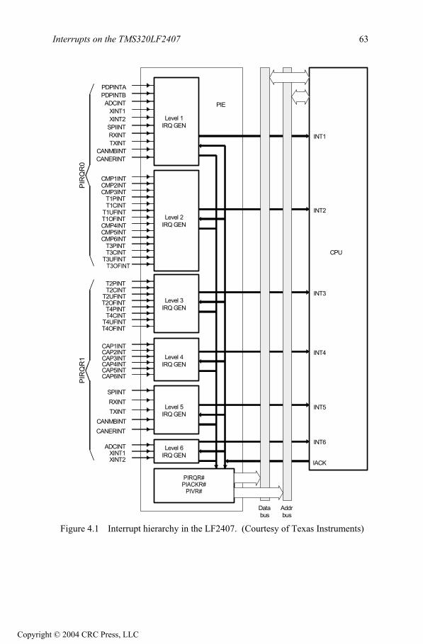
Interrupts on the TMS320LF2407 63
PIE
CPU
IACK
busAddr
busData
PIRQR#PIACKR#
PIVR#
IRQ GENLevel 6
IRQ GENLevel 5
IRQ GENLevel 4
IRQ GENLevel 2
IRQ GENLevel 1
XINT2XINT1
ADCINT
CANERINTCANMBINT
TXINTRXINTSPIINT
CAP3INTCAP2INTCAP1INT
T2OFINTT2UFINT
T2CINTT2PINT
T1OFINTT1UFINT
T1CINTT1PINT
CMP3INTCMP2INTCMP1INT
CANERINTCANMBINT
TXINTRXINTSPIINTXINT2XINT1
ADCINT
PDPINTA
IRQ GENLevel 3
INT1
INT2
INT3
INT4
INT5
INT6
PIR
QR
0PI
RQ
R1
PDPINTB
T3OFINTT3UFINT
T3CINTT3PINT
CMP6INTCMP5INTCMP4INT
T4OFINTT4UFINT
T4CINTT4PINT
CAP6INTCAP5INTCAP4INT
Figure 4.1 Interrupt hierarchy in the LF2407. (Courtesy of Texas Instruments)
Copyright © 2004 CRC Press, LLC

64 Interrupts on the TMS320LF2407
4.2.2 Reset and Non-Maskable Interrupts
There are two special interrupts on the LF2407 which have not been covered thus far; the Reset (RS) and the Non-Maskable Interrupt (NMI). Both of these interrupts bypass the usual interrupt hierarchy and feed straight to the DSP core. A reset causes the core to branch to address 0000h in program memory. Resets are activated during power on, when the external RESET pin is brought to logic “0” (O Volts), or by the Watchdog Timer. If the Watchdog is not disabled, it will pull the reset pin to “0” if not periodically reset.
When an illegal memory space is written to, the illegal address flag (ILLADR) in System Control and Status Register 1 (SCSR1) will be set. When this flag is set, a non-maskable interrupt (NMI) will be generated, causing the core to branch to address 0024h in program memory. The illegal address flag (ILLADR) will remain set following an illegal address condition until it is cleared by software or a DSP reset.
4.3 Interrupt Control Registers
This section will review the interrupt control registers. The IFR, IMR, and PIVR registers as well as the INTM bit discussed in the previous section will be presented in more detail. We will not discuss peripheral level interrupt bits in this chapter, as they will be discussed in each section dealing with the specific peripherals.
There are three registers used at the CPU level, the Interrupt Flag Register (IFR), the Interrupt Mask Register (IMR), and the Peripheral Interrupt Vector Register (PIVR). The IFR and IMR control the interrupt signal at the beginning of the CPU level. The PIVR register, while actually loaded in the PIE, provides information about the specific interrupt that occurred at the peripheral level. This information can be used by the ISR in determining the source of the interrupt signal. In addition to these registers, the INTM bit at the CPU level provides the final “gateway” that the interrupt signal must pass through to reach the core itself.
In addition to the peripheral interrupts, there are two External Interrupts (XINT1, XINT2). Their interrupt request operation is exactly like the peripheral interrupts. However, external interrupts are triggered by a logic edge transition on their external pin. The external interrupt control registers will also be discussed.
4.3.1 Interrupt Flag Register (IFR)
The IFR is a 16-bit (only 6 bits are really used) register mapped to address 0006h in data memory. The IFR is used to identify and clear pending interrupts at the CPU level and contains the interrupt flag bits for the maskable interrupt priorities INT1–INT6.
A flag bit in the IFR is set to “1” when an individual interrupt request signal makes its way out of the peripheral level and into the CPU level. The particular flag
Copyright © 2004 CRC Press, LLC

Interrupts on the TMS320LF2407 65
bit set depends on what priority the individual interrupt is grouped under. After theinterrupt is serviced, the IFR bit corresponding to the interrupt is automaticallycleared (to “0”) by the DSP.
In addition to triggering the CPU level during the standard interrupt process,the IFR can also be read by software. If a desired situation occurred where theINTM bit was set (meaning no interrupt signals make it to the core) and an interruptsignal was generated at the below levels, the corresponding bit in the IFR wouldstill be set. In this situation, the IFR could be read by software to identify pendinginterrupt requests.
If desired, to “manually” clear a bit in the IFR, software needs to write a “1” to the appropriate bit (see IFR bit descriptions). The flag bits can be thought of as“toggling” when a “1” is written to them. Loading the IFR into the accumulator,then storing the contents of the IFR back into itself clears all bits in the IFR. However, if the peripheral level interrupt flag bit is still set, the corresponding bit inthe IFR will immediately become set right after it is cleared.
Notes:
1. To clear an IFR bit, we must write a one to it, not a zero.2. When an interrupt is acknowledged, only the IFR bit is cleared
automatically. The flag bit in the corresponding peripheral controlregister is not automatically cleared. If an application requires that thecontrol register flag be cleared, the bit must be cleared by software.
3. IFR registers pertain to interrupts at the CPU level only. All peripheralshave their own interrupt mask and flag bits in their respectivecontrol/configuration registers.
4. When an interrupt is requested by the INTR assembly instruction and thecorresponding IFR bit is set, the CPU does not clear the bit automatically.If an application then requires that the IFR bit needs to be cleared, the bitmust be cleared by software.
Interrupt Flag Register (IFR) — Address 0006h
15-6 5 4 3 2 1 0
Reserved INT6 flag INT5 flag INT4 flag INT3 flag INT2 flag INT1 flag
0 RW1C–0 RW1C–0 RW1C–0 RW1C–0 RW1C–0 RW1C–0
Note: 0 = always read as zeros, R = read access, W1C = write 1 to this bit to clearit, -0 = value after reset.
Bits 15–6 Reserved. These bits are always read as zeros.
Bit 5 INT6. Interrupt 6 flag. This bit is the flag for interrupts connected to interrupt level INT6.0 No INT6 interrupt is pending
Copyright © 2004 CRC Press, LLC

66 Interrupts on the TMS320LF2407
1 At least one INT6 interrupt is pending. Write a 1 to this bit to clear it to 0 and clear the interrupt request
Bit 4 INT5. Interrupt 5 flag. This bit is the flag for interrupts connected to interrupt level INT5. 0 No INT5 interrupt is pending 1 At least one INT5 interrupt is pending. Write a 1 to this bit to
clear it to 0 and clear the interrupt request
Bit 3 INT4. Interrupt 4 flag. This bit is the flag for interrupts connected to interrupt level INT4. 0 No INT4 interrupt is pending 1 At least one INT4 interrupt is pending. Write a 1 to this bit to
clear it to 0 and clear the interrupt request
Bit 2 INT3. Interrupt 3 flag. This bit is the flag for interrupts connected to interrupt level INT3. 0 No INT3 interrupt is pending 1 At least one INT3 interrupt is pending. Write a 1 to this bit to
clear it to 0 and clear the interrupt request
Bit 1 INT2. Interrupt 2 flag. This bit is the flag for interrupts connected to interrupt level INT2. 0 No INT2 interrupt is pending 1 At least one INT2 interrupt is pending. Write a 1 to this bit to
clear it to 0 and clear the interrupt request
Bit 0 INT1. Interrupt 1 flag. This bit is the flag for interrupts connected to interrupt level INT1. 0 No INT1 interrupt is pending 1 At least one INT1 interrupt is pending. Write a 1 to this bit to
clear it to 0 and clear the interrupt request
4.3.2 Interrupt Mask Register (IMR)
The Interrupt Mask Register (IMR) is a 16-bit (only 6 bits are used) register located at address 0004h in data memory. It contains a mask bits for each of the six interrupt priority levels INT1–INT6. When an IMR bit is “0”, the corresponding interrupt is “masked”. When an interrupt is masked, the interrupt will be halted at the CPU level; the core will not be able to receive the interrupt request signal, regardless of the INTM bit status. When the interrupt’s IMR bit is set to “1”, the interrupt will be acknowledged if the corresponding IFR bit is “1” and the INTM bit is “0”. The IMR may also be read to identify which interrupts are masked or unmasked.
Copyright © 2004 CRC Press, LLC
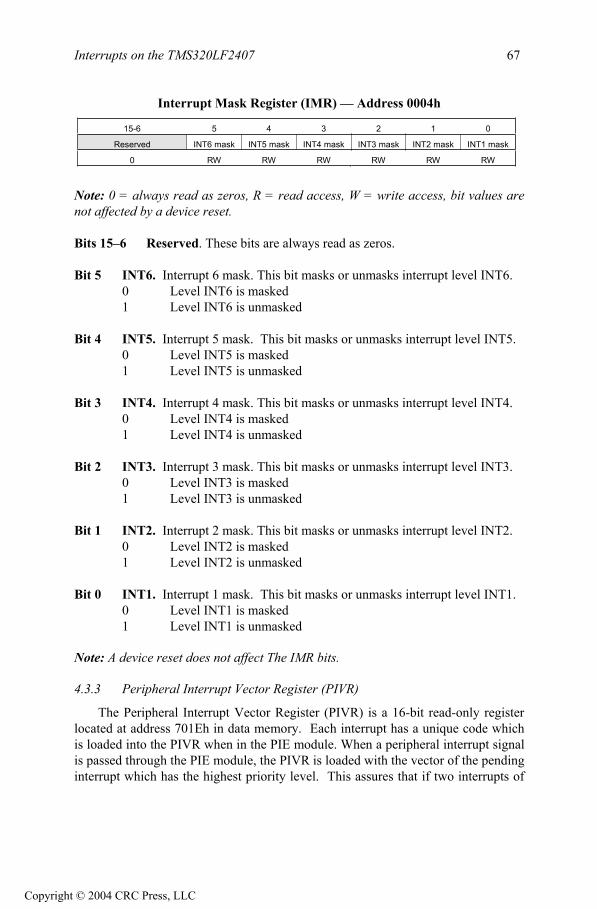
Interrupts on the TMS320LF2407 67
Interrupt Mask Register (IMR) — Address 0004h
15-6 5 4 3 2 1 0
Reserved INT6 mask INT5 mask INT4 mask INT3 mask INT2 mask INT1 mask
0 RW RW RW RW RW RW
Note: 0 = always read as zeros, R = read access, W = write access, bit values arenot affected by a device reset.
Bits 15–6 Reserved. These bits are always read as zeros.
Bit 5 INT6. Interrupt 6 mask. This bit masks or unmasks interrupt level INT6.0 Level INT6 is masked1 Level INT6 is unmasked
Bit 4 INT5. Interrupt 5 mask. This bit masks or unmasks interrupt level INT5.0 Level INT5 is masked1 Level INT5 is unmasked
Bit 3 INT4. Interrupt 4 mask. This bit masks or unmasks interrupt level INT4.0 Level INT4 is masked1 Level INT4 is unmasked
Bit 2 INT3. Interrupt 3 mask. This bit masks or unmasks interrupt level INT3.0 Level INT3 is masked1 Level INT3 is unmasked
Bit 1 INT2. Interrupt 2 mask. This bit masks or unmasks interrupt level INT2.0 Level INT2 is masked1 Level INT2 is unmasked
Bit 0 INT1. Interrupt 1 mask. This bit masks or unmasks interrupt level INT1.0 Level INT1 is masked1 Level INT1 is unmasked
Note: A device reset does not affect The IMR bits.
4.3.3 Peripheral Interrupt Vector Register (PIVR)
The Peripheral Interrupt Vector Register (PIVR) is a 16-bit read-only registerlocated at address 701Eh in data memory. Each interrupt has a unique code whichis loaded into the PIVR when in the PIE module. When a peripheral interrupt signalis passed through the PIE module, the PIVR is loaded with the vector of the pendinginterrupt which has the highest priority level. This assures that if two interrupts of
Copyright © 2004 CRC Press, LLC

68 Interrupts on the TMS320LF2407
different priorities happen simultaneously, the higher priority interrupt will beserviced first.
Peripheral Interrupt Vector Register (PIVR) — Address 701Eh
Note: R = read access, -0 = value after reset.
Bits 15–0 V15–V0. Interrupt vector. This register contains the peripheralinterrupt vector of the most recently acknowledged peripheral interrupt.
External Interrupt Control Registers
The external interrupts (XINT1, XINT2) are controlled by the XINT1CR and XINT2CR control registers, respectively. If these interrupts are enabled in theircontrol registers, an interrupt will be generated when the XINT1 or XINT2 logictransition occurs for at least 12 CPU clock cycles.
For example, if XINT1 was configured for generating an interrupt on a low (0Volts) to high (3.3 Volts) transition and the XINT1 pin only went high for 6 clockcycles, then back down to low, an interrupt request would not occur. However, if the pin was brought high for 12 or more cycles, an interrupt request signal would be generated.
External Interrupt 1 Control Register (XINT1CR) – Address 7070h
Note: R = read access, W = write access, C = clear by writing a 1, -0 = value afterreset.
Bit 15 XINT1 FlagThis bit indicates if the selected transition has been detected onthe XINT1 pin and is set whether or not the interrupt is enabled.This bit is cleared by software writing a 1 (writing a 0 has noeffect), or by a device reset.
0 No transition detected1 Transition detected
Copyright © 2004 CRC Press, LLC

Interrupts on the TMS320LF2407 69
Note: the description in the TI user guide can be misleading: this bit is not clearedautomatically during the interrupt acknowledge sequence.Bits 14–3 Reserved. Reads return zero; writes have no effect.
Bit 2 XINT1 PolarityThis read/write bit determines if interrupts are generated on therising edge or the falling edge of a signal on the pin.
0 Interrupt generated on a falling edge (high-to-low transition)1 Interrupt generated on a rising edge (low-to-high transition)
Bit 1 XINT1 PriorityThis read/write bit determines which interrupt priority isrequested. The CPU interrupt priority levels corresponding to lowand high priority are coded into the peripheral interrupt expansioncontroller. These priority levels are shown in Table 2–2, 240xAInterrupt Source Priority and Vectors, in Chapter 2 on page 2-9.
0 High priority1 Low priority
Bit 0 XINT1 EnableThis read/write bit enables or disables external interrupt XINT1.
0 Disable interrupt1 Enable interrupt
External Interrupt 2 Control Register (XINT2CR) – Address 7071h
Note: R = read access, W = write access, C = Clear by writing a 1, -0 = value afterreset.
Bit 15 XINT2 FlagThis bit indicates if the selected transition has been detected onthe XINT2 pin and is set whether or not the interrupt is enabled. This bit is cleared by software writing a 1 (writing a 0has no effect), or by a device reset.
0 No transition detected1 Transition detected
Note: the description in the TI user guide can be misleading: this bit is not clearedautomatically during the interrupt acknowledge sequence.
Copyright © 2004 CRC Press, LLC

70 Interrupts on the TMS320LF2407
Bits 14–3 Reserved. Reads return zero; writes have no effect.
Bit 2 XINT2 Polarity This read/write bit determines if interrupts are generated on the
rising edge or the falling edge of a signal on the pin. 0 Interrupt generated on a falling edge (high-to-low transition) 1 Interrupt generated on a rising edge (low-to-high transition)
Bit 1 XINT2 Priority This read/write bit determines which interrupt priority is
requested. The CPU interrupt priority levels corresponding to low and high priority are coded into the peripheral interrupt expansion controller. These priority levels are shown in Table 2–2, 240xA Interrupt Source Priority and Vectors, in Chapter 2 on page 2-9.
0 High priority 1 Low priority
Bit 0 XINT2 Enable This read/write bit enables or disables the external interrupt
XINT2. 0 Disable interrupt 1 Enable interrupt
4.4 Initializing and Servicing Interrupts in Software
In order to utilize the interrupt functions of the LF2407, several steps should be taken to initialize the DSP and interrupt related registers. This will assure that no false interrupts are asserted. While it is unlikely that a false interrupt would be generated, writing code that would ignore a false interrupt is good practice.
Servicing the interrupt requires that a few steps also be taken to “reset” the interrupt so that future interrupts of the same origin can also occur.
4.4.1 Configuring the LF2407 for Interrupt Operation
Several steps should be performed via software to prepare the DSP and interrupt system for use before any sort of algorithm is entered. The following provides for a general procedure for initializing the DSP interrupts and peripherals:
1. The first instruction after the START label should be to set the INTM bit. This assures that no interrupts can occur during initialization.
2. Once the INTM bit is set, then the second step is to mask each of the six CPU level interrupts by writing “0” to the IMR.
3. Once all bits in the IMR are “0”, the IFR value should be loaded into the accumulator, and then the accumulator should be written to the IFR. This writes the IFR back into itself, thereby clearing all flag bits.
Copyright © 2004 CRC Press, LLC

Interrupts on the TMS320LF2407 71
4. Now is the time to disable the Watchdog timer by writing “6Fh” to the WDCR (watchdog control register). Also, the DSP should be configured by setting the System Control Registers (SCSR1,SCSR2) for desired operation and the enabling the clock to desired peripherals.
5. If applicable, set the reset bit in the selected peripheral control registers. Configure peripheral for desired operation.
6. Configure the IMR to unmask only those interrupt levels which correspond to the selected peripheral.
7. Clear the INTM bit to allow future interrupts to reach the CPU. 8. If applicable, bring the selected peripherals out of reset/enable operation
via peripheral control register.
Example 4.1 - The following block is a segment of code which provides an example of interrupt initialization.
START:LDP #0h ;set DP=0 SETC INTM ;Disable interrupts SPLK #0000h,IMR ;Mask all core interrupts LACC IFR ;Read Interrupt flags SACL IFR ;Clear all interrupt flags LDP #WDKEY >> 7h ;Peripheral page SPLK #006Fh, WDCR ;Disable WD if VCCP=5V SPLK #0000h, SCSR1 ;
KICK_DOG SPLK #0h,GPR0 ;Set wait state generator for: OUT GPR0,WSGR ;Program Space, 0-7 wait states LDP #0E1h SPLK #00004h, MCRA ;Configure XINT pin for primary LDP #0E0h SPLK #5h, XINT1CR ;Configures XINT1 pin for
;polarity(low to high) priority(high), ;and enable bit
LDP # 0h SPLK #1, IMR ;XINT is INT1 so set IMR to “1” CLRC INTM ;Enables interrupts to core
LOOP B LOOP ;loops here until interrupt occurs
The above code will enable the XINT1 pin to generate an interrupt of INT1 when a “low to high” transition is detected on the pin.
4.4.2 Servicing Interrupts
Each of the interrupt priority levels INT1 through INT6 has a corresponding memory address 0001h through 0006h in program memory to which the core will branch upon receiving the interrupt. The header file vector.h assigns the labels “INT1, INT2, …INT6” to addresses 0001h through 0006h. This header file also instructs the core to branch to the corresponding General Interrupt Service Routines (GISR1 through GISR6) labels which are located in the assembly source file.
It is under the appropriate “GISRx” label in the source file where the interrupt service routine (ISR) is written. In the ISR, a variety of algorithms may be used. The ISR is simply an algorithm to which the core will execute whenever it
Copyright © 2004 CRC Press, LLC

72 Interrupts on the TMS320LF2407
encounters an interrupt. The first action in the ISR should be to perform a “context save” by saving the value of the accumulator, status registers, and anything else that could change as a result of the ISR, so that when the core exits from the interrupt, it is essentially in the same state as when it entered.
If multiple peripheral interrupts in the same priority level are enabled, then each of these interrupts would cause the core to branch to the same GISRx. In this case, it would be necessary to first run a PIVR reading and selection algorithm under the GISR which would determine what specific interrupt actually occurred. Then the algorithm would then branch to a Specific Interrupt Service Routine (SISR). Example 4.2 is pseudo-code which is an example of the selection algorithm discussed previously.
Example 4.2 – Two peripheral interrupts (RXINT and TXINT) are both assigned to priority level INT1. The following pseudo-code is a sample algorithm to determine which interrupt occurred and service the interrupt. ----------------------------------------------------------------------------------------------- GISR1 - GISR1 corresponds to ONLY INT1 interrupts Read the PIVR Does the PIVR contain the vector for RXINT ? Yes – Branch to R_ISR No – Continue to next instruction Does the PIVR contain the vector for TXINT? Yes – Branch to T_ISR No – Branch to ERROR R_ISR This would be the first SISR, the name of the SISR does not matter User defined algorithm plus reset interrupt for next occurrence and exit ISR
T_ISRThis would be the second SISR, the name of the SISR does not matter User defined algorithm plus reset interrupt for next occurrence and exit ISR ERRORUser defined algorithm plus reset interrupt for next occurrence and exit ISR ------------------------------------------------------------------------------------------------
Interrupt Vectors
Information on the different peripheral interrupts and their corresponding PIVR codes can be found in Table 4.1, which lists the peripheral interrupt vector codes that load into the PIVR. The vector is essentially an identification number for each interrupt. Note that an interrupt may have a different overall priority and grouping based on the (low or high) priority level that the interrupt is set to in its corresponding peripheral control register. For example, XINT1 (high priority) is assigned vector 0001h and is grouped INT1 with overall priority 7. XINT1 (low priority) is still assigned vector 0001h but is grouped INT6 with overall priority 33.
Copyright © 2004 CRC Press, LLC

Interrupts on the TMS320LF2407 73
Table 4.1 Interrupt vectors. (Courtesy of Texas Instruments)OverallPriority
InterruptName
CPUInterruptVector
PeripheralInterruptVector
Maskable? SourcePeripheral
Description
1 Reset RSN0000h
N/A N RS Pin,Watchdog
Reset from pin,watchdog time out
2 Reserved -0026h
N/A N CPU Emulator trap
3 NMI NMI0024h
N/A N Nonmaskableinterrupt
Nonmaskable interrupt
(a) INT1 (level 1)
OverallPriority
InterruptName
CPUInterruptVector
PeripheralInterruptVector
Maskable? SourcePeripheral
Description
4 PDPINTA INT10002h
0020h Y EVA Power drive protectioninterrupt pin
5 PDPINTB INT10002h
0019h Y EVB Power drive protectioninterrupt pin
6 ADCINT INT10002h
0004h Y ADC ADC interrupt in high–priority mode
7 XINT1 INT10002h
0001h Y Externalinterrupt logic
External interrupt pin inhigh–priority mode
8 XINT2 INT10002h
0011h Y Externalinterrupt logic
External interrupt pin inhigh–priority mode
9 SPIINT INT10002h
0005h Y SPI SPI interrupt in high–priority mode
10 RXINT INT10002h
0006h Y SCI SCI receiver interrupt inhigh–priority mode
11 TXINT INT10002h
0007h Y SCI SCI transmitter interruptin high–priority mode
12 CANMBINT INT10002h
0040h Y CAN CAN mailbox interrupt(high–priority mode)
13 CANERINT INT10002h
0041h Y CAN CAN error interrupt(high–priority mode)
(b) INT2 (level 2)
OverallPriority
InterruptName
CPUInterruptVector
PeripheralInterruptVector
Maskable? SourcePeripheral
Description
14 CMP1INT INT20004h
0021h Y EVA Compare 1 interrupt
15 CMP2INT INT20004h
0022h Y EVA Compare 2 interrupt
16 CMP3INT INT20004h
0023h Y EVA Compare 3 interrupt
17 T1PINT INT20004h
0027h Y EVA Timer 1 period interrupt
18 T1CINT INT20004h
0028h Y EVA Timer 1 compareinterrupt
19 T1UFINT INT20004h
0029h Y EVA Timer 1 underflowinterrupt
20 T1OFINT INT20004h
002Ah Y EVA Timer 1 overflowinterrupt
21 CMP4INT INT20004h
0024h Y EVB Compare 4 interrupt
22 CMP5INT INT20004h
0025h Y EVB Compare 5 interrupt
23 CMP6INT INT20004h
0026h Y EVB Compare 6 interrupt
24 T3PINT INT20004h
002Fh Y EVB Timer 3 period interrupt
25 T3CINT INT20004h
0030h Y EVB Timer 3 compareinterrupt
26 T3UFINT INT20004h
0031h Y EVB Timer 3 underflowinterrupt
27 T3OFINT INT20004h
0032h Y EVB Timer 3 overflowinterrupt
Copyright © 2004 CRC Press, LLC

74 Interrupts on the TMS320LF2407
(c) INT3 (level 3)
OverallPriority
InterruptName
CPUInterruptVector
PeripheralInterruptVector
Maskable? SourcePeripheral
Description
28 T2PINT INT30006h
002Bh Y EVA Timer 2 period interrupt
29 T2CINT INT30006h
002Ch Y EVA Timer 2 compareinterrupt
30 T2UFINT INT30006h
002Dh Y EVA Timer 2 underflowinterrupt
31 T2OFINT INT30006h
002Eh Y EVA Timer 2 overflowinterrupt
32 T4PINT INT30006h
0039h Y EVB Timer 4 period interrupt
33 T4CINT INT30006h
003Ah Y EVB Timer 4 compareinterrupt
34 T4UFINT INT30006h
003Bh Y EVB Timer 4 undeflowinterrupt
35 T4OFINT INT30006h
003Ch Y EVB Timer 4 overflowinterrupt
(d) INT4 (level 4)
OverallPriority
InterruptName
CPUInterruptVector
PeripheralInterruptVector
Maskable? SourcePeripheral
Description
36 CAP1INT INT40008h
0033h Y EVA Capture 1 interrupt
37 CAP2INT INT40008h
0034h Y EVA Capture 2 interrupt
38 CAP3INT INT40008h
0035h Y EVA Capture 3 interrupt
39 CAP4INT INT40008h
0036h Y EVB Capture 4 interrupt
40 CAP5INT INT40008h
0037h Y EVB Capture 5 interrupt
41 CAP6INT INT40008h
0038h Y EVB Capture 6 interrupt
(e) INT5 (level 5)
OverallPriority
InterruptName
CPUInterruptVector
PeripheralInterruptVector
Maskable? SourcePeripheral
Description
42 SPIINT INT5000Ah
0005h Y SPI SPI interrupt(low priority)
43 RXINT INT5000Ah
0006h Y SCI SCI receiver interrupt(low–priority mode)
44 TXINT INT5000Ah
0007h Y SCI SCI transmitterinterrupt (low–prioritymode)
45 CANMBINT INT5000Ah
0040h Y CAN CAN mailbox interrupt(low–priority mode)
46 CANERINT INT5000Ah
0041h Y CAN CAN error interrupt(low–priority mode)
(f) INT6 (level 6)
OverallPriority
InterruptName
CPUInterruptVector
PeripheralInterruptVector
Maskable? SourcePeripheral
Description
47 ADCINT INT6000Ch
0004h Y ADC ADC interrupt(low priority)
48 XINT1 INT6000Ch
0001h Y Externalinterrupt logic
External interrupt pins(low–priority mode)
49 XINT2 INT6000Ch
0011h Y Externalinterrupt logic
External interrupt pins(low–priority mode)
Reserved 000Eh N/A Y CPU Analysis interrupt
N/A TRAP 0022h N/A N/A CPU TRAP instruction
N/A PhantomInterruptVector
N/A 0000h N/A CPU Phantom interruptvector
Copyright © 2004 CRC Press, LLC

Interrupts on the TMS320LF2407 75
4.5 Interrupt Usage Exercise
This exercise will help the reader become familiar with interrupt operation and writing interrupt service routines in software. The skills practiced in this exercise are extremely relevant in sequential chapters where interrupts must be understood for peripheral use.
1. Create a new project and source file each named “lab4”. Add the same header files as in previous exercises.
2. Create a program which first properly configures the LF2407 and XINT1 interrupt registers for operation on a low to high clock edge. On the LF2407 EVM module, jumper the XF pin the XINT1. Configure the XF pin to initially output logic “0”. The program should utilize a looping algorithm and the XINT1 interrupt to perform the following tasks:
a. Start with the value “0h” in the accumulator. Store the number in the accumulator to the data memory address 300h. When this operation is complete, set the XF pin to be “1” (logic high). This should trigger an XINT1 interrupt.
b. In the ISR, keep count of the number of interrupts generated in the address “030Fh”. Start counting at “0” for the first interrupt generated. Reset the XF pin to logic “0”. Re-enable the interrupt.
c. Keep repeating steps (a) and (b), but use the numbers “0001h” through “000Ah” instead and store them to memory address 301h through 30Ah.
The program should store a total of 11 numbers (0h to Ah) to memory addresses 300h through 30Ah. There should be exactly 11 interrupts counted with the number “Ah” stored in memory address 30Fh.
d. After steps (a) through (c) are complete, perform the calculations “Ah” multiplied by “3h” , “1h” multiplied by “5h”, and “11h” multiplied by “7h” one after the other. Create a transition on the XF pin so an XINT1 interrupt will be generated after each calculation is complete. Count the number of these interrupts and store them in data memory address 310h.
When the program is finished with the task, have it loop infinitely until halted by the user. This exercise is now concluded.
Copyright © 2004 CRC Press, LLC

Chapter 5
THE ANALOG-TO-DIGITAL CONVERTER (ADC)
5.1 ADC Overview
The Analog-to-Digital Converter (ADC) on the LF2407 allows the DSP to sample analog or “real-world” voltage signals. The output of the ADC is an integernumber which represents the voltage level sampled. The integer number may be used for calculations in an algorithm. The resolution of the ADC is 10 bits,meaning that the ADC will generate a 10-bit number for every conversion itperforms. However, the ADC stores the conversion results in registers that are 16 bits wide. The 10 most significant bits are the ADC result, while the least significant bits (LSBs) are filled with “0”s. We usually want to truncate the uselesszeros, so the value in the result register is simply right shifted by six places.
If the ADC performs a conversion on a 3.3V signal, it will theoreticallygenerate “1111111111000000b” (or “FFC0h”) in the appropriate result register and“0h” if a 0V signal is sampled. In actuality, the least significant of the 10 bits will vary slightly; this is the result of random noise picked up by the ADC.
There are a total of 16 input channels to the single input ADC. The controllogic of the ADC consists of auto-sequencers, which control the sampling of the 16input channels to the ADC. The auto-sequencers not only control which channels(input channels) will be sampled by the ADC, but also the order of the channels thatthe ADC performs conversions on. The two 8-conversion auto-sequencers canoperate independently or cascade together as a “virtual” 16-conversion ADC.
5.1.1 Summary of the LF2407 ADC
10-bit ADC with built-in Sample and Hold (S/H)Fast conversion time of 500 nsSixteen (16) multiplexed analog inputs (ADCIN0 – ADCIN15)Auto-sequencing capability – up to 16 “auto-conversions” in a singlesession. Each conversion session can be programmed to select any one ofthe 16 input channelsTwo independent 8-state sequencers (SEQ1 and SEQ2) that can beoperated individually in dual-sequencer mode or cascaded into one large16-state sequencer (SEQ) in cascaded modeFour Sequencing Control Registers (CHSELSEQ1..4) that determine thesequence of analog channels that are taken up for conversion in a givensequencing modeSixteen (individually addressable) result registers to store the convertedvalues (RESULT0 – RESULT15)Multiple trigger sources for start-of-conversion (SOC) a. Software: Software start (using SOC SEQn bit)b. EVA: Event manager A (multiple event sources within EVA)
77
Copyright © 2004 CRC Press, LLC

The Analog-to-Digital Converter (ADC)78
c. EVB: Event manager B (multiple event sources within EVB)d. External: ADCSOC pinInterrupt control allows interrupt generation on every end-of-sequence(EOS) or every other EOSSequencer can operate in start/stop mode, allowing multiple time-sequenced triggers to synchronize conversionsEVA and EVB can independently trigger SEQ1 and SEQ2, respectively(this is applicable for dual-sequencer mode only)Sample-and-hold acquisition time window has separate prescale controlBuilt-in calibration mode and built-in self-test mode
5.2 Operation of the ADC
Using the ADC on the LF2407 is relatively simple. The user first needs toconfigure the ADC for the desired operation. Like all peripherals, all registersrelating to ADC operation have addresses in data memory space. The first step in configuring the ADC should be to reset the ADC. After the ADC is reset, the nextstep is to configure the main ADC control registers (ADCTRL1, ADCTRL2) for desired ADC operation. Then, load the MAXCONV register with the desirednumber of automatic conversions minus 1. For example, if seven auto-conversionsare desired, MAXCONV would be loaded with “6”. The desired input channels andtheir order of conversion need to be specified in the CHSELSEQn registers.Finally, a SOC trigger will start the sampling process. A short example of theassembly code performing the above listed steps is provided in Example 5.1.
Example 5.1- The following code gives an example of initializing the ADC, settingup the CHSELSEQn registers and starting the conversion sequence:
LDP #0E1h SPLK #0100000000000000b,ADCTRL1 NOPSPLK #0011000000010000b,ADCTRL1
; the following explains bits in ADCCTRL1: ; 15 - RSVD | 14 - Reset(1) | 13,12 - Soft & Free ; 11,10,9,8 - Acq. prescalers | 7 - Clock prescaler ; 6 - Cont. run (1) | 5 - Int. priority (Hi.0) ; 4 - Seq. casc (0-dual)
SPLK #15, MAXCONV ;Setup for 16 conversions SPLK #03210h, CHSELSEQ1 ;Conv Ch 0,1,2,3 SPLK #07654h, CHSELSEQ2 ;Conv Ch 4,5,6,7 SPLK #0BA98h, CHSELSEQ3 ;Conv Ch 8,9,10,11 SPLK #0FEDCh, CHSELSEQ4 ;Conv Ch 12,13,14,15 SPLK #2000b, ADCTRL2 ;Start the conversions by bit 13
After the conversion process is complete, each 10-bit result can be read fromthe result registers RESULTn. The conversion results are stored sequentially inresult registers RESULT0 to RESULT15. The first result is stored in RESULT0, thesecond result in RESULT1, and so on. For example, if ADC channel 1 is selectedfor four consecutive conversions, the results will appear in registers RESULT0
Copyright © 2004 CRC Press, LLC

The Analog-to-Digital Converter (ADC) 79
through RESULT3. There is no correlation between ADC Channel 1 and theRESULT register 1 or Channel 2 and RESULT 2 etc.
We will discuss each of these steps in detail in the following sections, startingwith the different operating modes of the ADC. This will aid the reader inconfiguring the ADC control registers by helping to determine what operating modeis needed. After the reader is familiar with the ADC operating modes, we willcover the MAXCONV and CHSELSEQn registers. Various SOC trigger methodswill then be discussed. Finally, the ADC conversion result register reading will bediscussed.
5.2.1 Sequencer Configurations of the ADC
The first operating parameter the user needs to select is to configure the ADCto operate as either one 16-conversion sequencer or two 8-conversion sequencers.The ADC sequencer consists of two independent 8-conversion sequencers (SEQ1and SEQ2) that can be cascaded together to form one 16-conversion sequencer(SEQ).
When the ADC is configured to operate as one cascaded 16-convesionsequencer, it may perform up to 16 conversions on any combination of the 16 inputchannels. For example, it could be programmed to perform 14 conversions onchannel 1, or in another instance, 10 total conversions on a combination of channelsdepending on what the CHSELSEQn registers are set for. The diagram Fig. 5.1shows the configuration of the cascaded 16-conversion sequencer. When incascaded mode there is only one sequencer (SEQ) and the MAXCONV register isprogrammed for the maximum number of conversions. The results are stored inRESULT0 through RESULT 15 depending on the number of conversionsperformed.
If the ADC is configured as two 8-conversion sequencers, then each sequenceroperates independently. When the two sequencers are used independently, thecurrent active sequencer has priority over the inactive one. The start of conversionrequest from the “inactive” sequencer will be taken as soon as the sequence initiatedby the “active” sequencer is completed. For example, if Sequencer 1 (SEQ1) iscurrently performing a conversion and Sequencer 2 (SEQ2) requests a start ofconversion, the ADC will finish the conversion from SEQ1, and then start the SEQ2conversion. See Fig. 5.2 for a diagram of the dual-sequencer configuration. In dual-sequencer operation, the MAXCONV register is “split” up so that the sameregister contains data for the maximum number of conversions for both SEQ1 andSEQ2. The 16 result registers are also split up so SEQ1 uses RESULT0 throughRESULT7 and SEQ2 uses RESULT8 through RESULT15. A summary of thecascaded and dual-sequencer configurations is listed in Table 5.1.
Copyright © 2004 CRC Press, LLC

The Analog-to-Digital Converter (ADC)80
ADCIN0ADCIN1ADCIN2
ADCIN15
MAX CONV1
Ch Sel (state 0) Ch Sel (state 1)
Ch Sel (state 3)Ch Sel (state 2)
Ch Sel (state 15)
Statepointer
10–bit, 375–ns†
S/H + A/D converter
4
SOC EOC
4
10
Analog MUX Result MUX
Resultselect
10
RESULT0
Autosequencerstate machine
Start–of–sequence triggerSoftware
EVAEVB
External pin (ADCSOC)
MUXselect
Note: Possible values are:Channel select = 0 to 15MAXCONV = 0 to 15
RESULT1
RESULT2
RESULT15
† 425–ns for LC2402A
Figure 5.1 Block diagram of ADC in cascaded sequencer mode. (Courtesy of
Texas Instruments)
Table 5.1 Comparasion table of dual (SEQ1 and SEQ2) versus cascaded
sequencer configuration
Feature Single 8–statesequencer #1 (SEQ1)
Single 8–statesequencer #2 (SEQ2)
Cascaded 16–statesequencer (SEQ)
Start–of–conversiontriggers
EVA, software,external pin
EVB, software EVA, EVB, software,external pin
Maximum number ofautoconversions(i.e., sequence length)
8 8 16
Autostop at end–of–sequence (EOS)
Yes Yes Yes
Arbitration priority High Low Not applicable
ADC conversion resultregister locations
0 to 7 8 to 15 0 to 15
CHSELSEQn bit fieldassignment
CONV00 to CONV07 CONV08 to CONV15 CONV00 to CONV15
Copyright © 2004 CRC Press, LLC
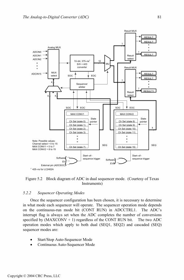
The Analog-to-Digital Converter (ADC) 81
ADCIN0ADCIN1ADCIN2
ADCIN15
MAX CONV1
Ch Sel (state 0)Ch Sel (state 1)
Ch Sel (state 3)Ch Sel (state 2)
Ch Sel (state 7)
Statepointer
10–bit, 375–ns†
S/H + A/Dconverter
SOC EOC
10
Analog MUX
Result MUX
Resultselect
1
RESULT
RESULT
RESULT
SEQ
SoftwareEV
External pin (ADCSOC)
MUXselect
Note: Possible values:Channel select = 0 to 15MAX CONV1 = 0 to 7
Sequencerarbiter
SOC EOC
4 4
4
MU
Ch Sel (state 15)
Ch Sel (state 8)Ch Sel (state 9)
Ch Sel (state 11)Ch Sel (state 10)
EVB
MAX CONV2
SOC EOC
4
Software
SEQ
Start–of–sequence trigger
Resultselect
RESULT11
Result MUX
RESULT
RESULT
1
1
MAX CONV2 = 8 to 15
Statepointer
Start–of–sequence trigger
† 425–ns for LC2402A
Figure 5.2 Block diagram of ADC in dual sequencer mode. (Courtesy of TexasInstruments)
5.2.2 Sequencer Operating Modes
Once the sequencer configuration has been chosen, it is necessary to determinein what mode each sequencer will operate. The sequencer operation mode dependson the continuous-run mode bit (CONT RUN) in ADCCTRL1. The ADC’sinterrupt flag is always set when the ADC completes the number of conversionsspecified by (MAXCONV + 1) regardless of the CONT RUN bit. The two ADCoperation modes which apply to both dual (SEQ1, SEQ2) and cascaded (SEQ)sequencer modes are:
Start/Stop Auto-Sequencer ModeContinuous Auto-Sequencer Mode
Copyright © 2004 CRC Press, LLC

The Analog-to-Digital Converter (ADC)82
Start/Stop Auto-Sequencer Mode
If the CONT RUN bit is not set, upon receiving a trigger, the ADC performs all conversions and halts at the last conversion state (CONVxx) in the corresponding CHSELSEQn. To perform another batch of conversions, the ADC is normally resetto its initial state via the RST SEQn bit in the ADCTRL2 register and reinitialized.After being reinitialized, another trigger is given and the whole process starts overagain. Figure 5.3 is a flowchart of the operation of the ADC under start/stop mode.
Current conversion complete. Digitalresult is written into corresponding
RESULTn register
Conversion begins. AUTO_SEQ_SRregister is decremented by one for every
conversion
MAXCONV value gets loadedinto AUTO_SEQ_SR register
SOC trigger arrives
Initialize the ADC registers
All ConversionsComplete?
(AUTO_SEQ_SR = 0 ?)
Set INT FLAG SEQn
No
Yes
Note: Flow chart corresponds to CONT RUN bit = 0.
Figure 5.3 Flowchart for Start/Stop Auto-Sequencer Mode (CONT RUN=0).
In the case when another trigger signal is given and the ADC has not beenreset, the ADC performs another specified number of conversions (MAXCONV +1) from the current conversion state and then halts. Another trigger signal willsimply restart the sequencer from the point where it halted. When the ADC is givenmultiple triggers without being reset in between, this operation is referred to as
Copyright © 2004 CRC Press, LLC

The Analog-to-Digital Converter (ADC) 83
multiple time-sequenced trigger operation. Example 5.2 illustrates a situation wherea multiple time-sequenced trigger operation might be used.
Example 5.2 – The following is a situation where a multiple time-sequenced triggeroperation might be used.
An application requires conversions on all 16 channels, but not all at once. Theapplication requires conversions on channels 0 through 3, perform a fewcalculations, convert channels 4 through 7, do a few more calculations, convert channels 8 through 11, etc. until conversions are performed on all 16 input channels.The four CHSELSEQ registers would be loaded only once with all 16 channels inthe desired order. The MAXCONV register would be loaded with the number “3”, which configures the auto-sequencer for four conversions. Each time the sequencerpauses, the algorithm would branch to the section of code that performs calculationsand retrigger the ADC. This “branching” could either occur as a result of aninterrupt or bit polling algorithm.
Continuous Auto-Sequencer Mode
The continuous-run mode bit is set to “1” for this mode of operation. When inthis mode, the ADC completes the number of conversions specified, resets itself to the first conversion state (CONV00), and then performs the whole operation overagain. This operation is similar to the start/stop mode except that the ADC is put in a continuous “looping” operation.
Note: If the CONT RUN (continuous run) mode is selected, the user must be surethat the result registers are read before the next conversion sequence begins. Thisis because every time the ADC runs, the result registers will be overwritten with themost current results.
5.2.3 Triggering Sources for the LF2407 ADC
In order to start the conversion sequence on the ADC, the sequencer must betriggered. There are several different trigger sources on the LF2407. Triggers maycome from a SOC signal from EVA: external pin or software. A software trigger isthe trigger thus far used as an example. The software trigger is generated by settingthe SOC SEQ1 bit (cascaded mode) or SOC SEQ1,2 bits (dual mode) in theADCTRL2 register. Other than software triggers, hardware in the form of an external pin or on-chip peripheral can also trigger the ADC. Table 5.2 lists thepossible triggering sources which generate a SOC for the ADC. Each trigger inputcan be enabled /disabled.
Copyright © 2004 CRC Press, LLC

The Analog-to-Digital Converter (ADC)84
Table 5.2 SOC Trigger Sources for the ADC
The following conditions apply to trigger operation:
a. A SOC trigger can initiate an auto-conversion sequence whenever asequencer is in an idle state. An idle state is either just after reset (CONV00), or any state where the sequencer has just finished aconversion sequence, i.e., when SEQ CNTR has reached zero.
b. If a SOC trigger occurs while a current conversion sequence isunderway, it sets the SOC SEQn bit. If yet another SOC triggeroccurs, that trigger is ignored. This basically operates as a SOC trigger “buffer” that will catch a trigger even though the ADC mightbe currently performing a conversion.
c. Once triggered, the sequencer cannot be stopped/halted in midsequence. The program must either wait until an End-of-Sequence(EOS) or initiate a sequencer reset, which brings the sequencerimmediately back to the idle start state (CONV00 for SEQ1 andcascaded cases; CONV08 for SEQ2).
d. When SEQ1 and SEQ2 are used in cascaded mode, triggers going to SEQ2 are ignored, while SEQ1 triggers are active. Cascaded modecan be viewed as SEQ1 with 16 conversion states instead of 8.
5.2.4 The ADCTRL1 and ADCTRL2 Control Registers
ADC Control Register 1 (ADCTRL1) — Address 70A0h
15 14 13 12 11 10 9 8
Reserved RESET SOFT FREE ACQ PS3 ACQ PS2 ACQ PS1 ACQ PS0
RS–0 RW–0 RW–0 RW–0 RW–0 RW–0 RW–0
7 6 5 4 3 2 1 0
CPS CONT RUN INT PRI SEQ CASC CAL ENA BRG ENA HI/LO STESTENA
RW–0 RW–0 RW–0 RW–0 RW-0 RW-0 RW-0 RW-0
Note: R = read access, W = write access, S = set only, -0 = value after reset.
Bit 15 Reserved
Copyright © 2004 CRC Press, LLC

The Analog-to-Digital Converter (ADC) 85
Bit 14 RESET. ADC module software reset. This bit causes a master reset on theentire ADC module. All register bits and sequencer state machines are reset to the initial state as occurs when the device reset pin is pulled low(or after a power-on reset).0 No effect1 Resets entire ADC module (bit is then set back to 0 by ADC
logic)
Note: Using the RESET Bit in the ADCTRL1 Register
The ADC module is reset during a system reset. If an ADC module reset isdesired at any other time, you can do so by writing a 1 to this bit. After a NOP, you can then write the appropriate values to the ADCTRL1 register
bits:SPLK #01xxxxxxxxxxxxxxb,ADCTRL1 ;Resets the ADC (RESET = 1)NOP ;Provides the required delay between
; two writes to the ADCTRL1SPLK #00xxxxxxxxxxxxxxb,ADCTRL1 ;Takes ADC out of Reset(RESET= 0)
Note: The second SPLK is not required if the default/power-on configuration of theADC is sufficient.
Bits 13, 12 SOFT and FREE. Soft and Free bits. These bits determine what happens with the ADC when an emulation-suspend occurs (due to thedebugger hitting a breakpoint, for example). In free-run mode, theperipheral can continue with whatever it is doing. In stop mode, theperipheral can either stop immediately or stop when the current operation(i.e., the current conversion) is complete.Soft Free 0 0 Immediate stop on suspend1 0 Complete current conversion before stoppingX 1 Free run, continue operation regardless of suspend
Bits 11–8 ACQ PS3 – ACQ PS0. Acquisition time window – pre-scale bits 3–0These bits define the ADC clock pre-scale factor applied to the acquisitionportion of the conversion and determine over what time period each ADcsample will take place. The pre-scale values are defined in the following table.
Copyright © 2004 CRC Press, LLC

The Analog-to-Digital Converter (ADC)86
Notes:
# ACQPS3
ACQPS2
ACQPS1
ACQPS0
PRE-SCALER(div. by)
AcquisitionTime
Window
SourceZ
(CPS=0)
SourceZ
(CPS=1)0 0 0 0 0 1 2 x Tclk 67 3851 0 0 0 1 2 4 x Tclk 385 10202 0 0 1 0 3 6 x Tclk 702 16553 0 0 1 1 4 8 x Tclk 1020 22904 0 1 0 0 5 10 x Tclk 1337 29255 0 1 0 1 6 12 x Tclk 1655 35606 0 1 1 0 7 14 x Tclk 1972 41947 0 1 1 1 8 16 x Tclk 2290 48298 1 0 0 0 9 18 x Tclk 2607 54649 1 0 0 1 10 20 x Tclk 2925 6099A 1 0 1 0 11 22 x Tclk 3242 6734B 1 0 1 1 12 24 x Tclk 3560 7369C 1 1 0 0 13 26 x Tclk 3877 8004D 1 1 0 1 14 28 x Tclk 4194 8639E 1 1 1 0 15 30 x Tclk 4512 9274F 1 1 1 1 16 32 x Tclk 4829 9909
1) Period of Tclk is dependent on the “Conversion Clock Prescale” bit (Bit 7); i.e.,CPS = 0: Tclk = 1/CLK (example, for CLK = 30 MHz, Tclk = 33 ns)CPS = 1: Tclk = 2(1/CLK) (example, for CLK = 30 MHz, Tclk = 66 ns)2) Source impedance Z is a design estimate only.
Bit 7 CPS. Conversion clock prescale. This bit defines the ADC conversionlogic clock prescale0 Fclk = CLK/11 Fclk = CLK/2CLK = CPU clock frequency
Bit 6 CONT RUN. Continuous runThis bit determines whether the sequencer operates in continuousconversion mode or start-stop mode. This bit can be written whilea current conversion sequence is active. This bit will take effect at the end of the current conversion sequence, i.e., software canset/clear this bit until EOS has occurred for valid action to be taken. In the continuous conversion mode, there is no need toreset the sequencer; however, the sequencer must be reset in thestart-stop mode to put the converter in state CONV00.
0 Start-stop mode. Sequencer stops after reaching EOS. This isused for multiple time-sequenced triggers.
1 Continuous conversion mode. After reaching EOS, the sequencerstarts all over again from state CONV00 (for SEQ1 and cascaded)or CONV08 (for SEQ2).
Copyright © 2004 CRC Press, LLC

The Analog-to-Digital Converter (ADC) 87
Bit 5 INT PRI. ADC interrupt request priority0 High priority1 Low priority
Bit 4 SEQ CASC. Cascaded sequencer operation. This bit determines whetherSEQ1 and SEQ2 operate as two 8-state sequencers or as a single 16-statesequencer (SEQ).0 Dual-sequencer mode. SEQ1 and SEQ2 operate as two 8-state sequencers.1 Cascaded mode. SEQ1 and SEQ2 operate as a single 16-state sequencer (SEQ).
Bit 3 CAL ENA. Offset calibration enableWhen set to 1, CAL ENA disables the input channel multiplexer,and connects the calibration reference selected by the bits HI/LO and BRG ENA to the ADC core inputs. The calibrationconversion can then be started by setting bit 14 of ADCTRL2register (STRT CAL) to 1. Note that CAL ENA should be set to 1first before the STRT CAL bit can be used.
Note: This bit should not be set to 1 if STEST ENA = 10 Calibration mode disabled1 Calibration mode enabled
Bit 2 BRG ENA. Bridge enableTogether with the HI/LO bit, BRG ENA allows a referencevoltage to be converted in calibration mode. See the description ofthe HI/LO bit for reference voltage selections during calibration.
0 Full reference voltage is applied to the ADC input1 A reference midpoint voltage is applied to the ADC input
Bit 1 HI/LO. VREFHI/VREFLO selectionWhen the fail self-test mode is enabled (STEST ENA = 1), HI/LOdefines the test voltage to be connected. In calibration mode,HI/LO defines the reference source polarity; see Table 7–5. Innormal operating mode, HI/LO has no effect.
0 VREFLO is used as precharge value at ADC input1 VREFHI is used as precharge value at ADC input
Copyright © 2004 CRC Press, LLC

The Analog-to-Digital Converter (ADC)88
Reference Bit Voltage Selection
BRG ENA HI/LO CAL ENA = 1Reference voltage (V)
STEST ENA = 1 Reference voltage (V)
0 0 VREFLO VREFLO
0 1 VREFHI VREFHI
1 0 |(VREFHI - VREFLO) / 2| VREFLO
1 1 |(VREFLO - VREFHI) / 2| VREFHI
Bit 0 STEST ENA. Self-test function enable0 Self-test mode disabled1 Self-test mode enabled
ADC Control Register 2 (ADCTRL2) — Address 70A1h
15 14 13 12 11 10 9 8
EVB SOCSEQ
RST SEQ1/STRT CAL
SOC SEQ1 SEQ1 BSY INT ENASEQ1
(Mode 1)
INT ENASEQ1
(Mode 0)
INT FLAGSEQ1
EVA SOCSEQ1
RW–0 RS–0 RW–0 R–0 RW–0 RW–0 RC–0 RW–0
7 6 5 4 3 2 1 0
EXT SOCSEQ1
RST SEQ2 SOC SEQ2 SEQ2 BSY INT ENASEQ2
(Mode 1)
INT ENASEQ2
(Mode 0)
INT FLAGSEQ2
EVB SOCSEQ2
RW–0 RS–0 RW–0 R–0 RW–0 RW–0 RC–0 RW–0
Note: R = read access, W = write access, S = set only, C = clear, -0 = value afterreset.
Bit 15 EVB SOC SEQ. EVB SOC enable for cascaded sequencer (Note: This bitis active only in cascaded mode.)0 No action1 Setting this bit allows the cascaded sequencer to be started by an
Event Manager B signal. The Event Manager can be programmedto start a conversion on various events. See Chapter 6 for details.
Bit 14 RST SEQ1 / STRT CAL. Reset Sequencer1/Start CalibrationCase: Calibration Disabled (Bit 3 of ADCTRL1) = 0Writing a 1 to this bit will reset the sequencer immediately to an initial “pre-triggered” state, i.e., waiting for a trigger at CONV00.A currently active conversion sequence will be aborted.
0 No action1 Immediately reset sequencer to state CONV00
Case: Calibration Enabled (Bit 3 of ADCTRL1) = 1Writing a 1 to this bit will begin the converter calibration process.
0 No action
Copyright © 2004 CRC Press, LLC

The Analog-to-Digital Converter (ADC) 89
1 Immediately start calibration process
Bit 13 SOC SEQ1. SOC trigger for Sequencer 1 (SEQ1). This bit can be set bythe following triggers:
S/W – Software writing a 1 to this bitEVA – Event Manager AEVB – Event Manager B (only in cascaded mode)EXT – External pin (i.e., the ADCSOC pin)
When a trigger occurs, there are three possibilities:
Case 1: SEQ1 idle and SOC bit clear. SEQ1 starts immediately (underarbiter control). This bit is set and cleared, allowing for any“pending” trigger requests.
Case 2: SEQ1 busy and SOC bit clear. Bit is set signifying a triggerrequest is pending. When SEQ1 finally starts after completingcurrent conversion, this bit will be cleared.
Case 3: SEQ1 busy and SOC bit set. Any trigger occurring in this case will be ignored (lost).
0 Clears a pending SOC trigger.
Note: If the sequencer has already started, this bit will automatically be cleared,and, hence, writing a zero will have no effect; i.e., an already started sequencercannot be stopped by clearing this bit.
1 Software trigger – Start SEQ1 from currently stopped position(i.e., idle mode)
Note: The RST SEQ1 (ADCTRL2.14) and the SOC SEQ1 (ADCTRL2.13) bitsshould not be set in the same instruction. This will reset the sequencer, but will notstart the sequence. The correct sequence of operation is to set the RST SEQ1 bitfirst, and the SOC SEQ1 bit in the following instruction. This ensures that thesequencer is reset and a new sequence started. This sequence applies to the RSTSEQ2 (ADCTRL2.6) and SOC SEQ2 (ADCTRL2.5) bits also.
Bit 12 SEQ1 BSY. SEQ1 Busy This bit is set to a 1 while the ADC auto-conversion sequence is in progress. It is cleared when the conversion sequence is complete.
0 Sequencer is idle (i.e., waiting for trigger)1 Conversion sequence is in progress
Bits 11–10 INT ENA SEQ1. Interrupt-mode-enable control for SEQ1
Copyright © 2004 CRC Press, LLC

The Analog-to-Digital Converter (ADC)90
Bit 11 Bit 10 Operation Description
0 0 Interrupt is disabled0 1 Interrupt Mode 1. Interrupt requested immediately when
INT FLAG SEQ1 flag is set 1 0 Interrupt Mode 2
Interrupt requested only if INT FLAG SEQ1 flag isalready set. If clear,† INT FLAG SEQ1 flag is set and INTrequest is suppressed. (This mode allows interruptrequests to be generated for every other EOS.)
1 1 Reserved
† This means that the last completed sequence is the first of the two sequences needed to assert an interrupt.
Bit 9 INT FLAG SEQ1. ADC interrupt flag bit for SEQ1This bit indicates whether an interrupt event has occurred or not.This bit must be cleared by the user writing a 1 to it.
0 No interrupt event1 An interrupt event has occurred
Checking for ADC Peripheral Interrupt Flag
After a SOC is initiated, we can check the INT FLAG SEQn bit to see if theresults are in the result registers.
Example code:
ADC_LOOP1:
LDP #0E1h ;data page - ADCTRL2
SPLK #0100000000000000b,ADCTRL2 ;Reset for SEQ1
NOP
NOP
NOP
NOP
SPLK #0010000000000000b,ADCTRL2 ;SOC for SEQ1
CHK_INTFLAG:
BIT ADCTRL2, 6 ;Wait for INT Flag to set
BCND CHK_INTFLAG, NTC ;If TC=0, keep looping.
Bit 8 EVA SOC SEQ1. Event Manager A SOC mask bit for SEQ1
Copyright © 2004 CRC Press, LLC

The Analog-to-Digital Converter (ADC) 91
0 SEQ1 cannot be started by EVA trigger.1 Allows SEQ1/SEQ to be started by Event Manager A trigger. The
Event Manager can be programmed to start a conversion onvarious events. See Chapter 6 for details.
Bit 7 EXT SOC SEQ1. External signal SOC bit for SEQ10 No action1 Setting this bit enables an ADC auto-conversion sequence to be
started by a signal from the ADCSOC device pin.
Bit 6 RST SEQ2. Reset SEQ20 No action1 Immediately resets SEQ2 to an initial “pre-triggered” state, i.e.,
waiting for a trigger at CONV08. A currently active conversionsequence will be aborted.
Bit 5 SOC SEQ2. SOC trigger for Sequencer 2 (SEQ2)(Only applicable in dual-sequencer mode; ignored in cascadedmode.)
This bit can be set by the following triggers:S/W – Software writing of 1 to this bitEVB – Event Manager B
When a trigger occurs, there are three possibilities:Case 1: SEQ2 idle and SOC bit clear
SEQ2 starts immediately (under arbiter control) and the bit is cleared, allowing for any pending trigger requests.
Case 2: SEQ2 busy and SOC bit clear Bit is set signifying a trigger request is pending. When SEQ2 finally starts after completing current conversion, this bit will becleared.
Case 3: SEQ2 busy and SOC bit setAny trigger occurring in this case will be ignored (lost).
0 Clears a pending SOC trigger.Note: If the sequencer has already started, this bit willautomatically be cleared, and hence, writing a zero will have noeffect; i.e., an already started sequencer cannot be stopped byclearing this bit.
1 Software trigger – Start SEQ2 from currently stopped position(i.e., idle mode)
Copyright © 2004 CRC Press, LLC

The Analog-to-Digital Converter (ADC)92
Bit 4 SEQ2 BSY. SEQ2 Busy
This bit is set to a 1 while the ADC auto-conversion sequence is in progress. It is cleared when the conversion sequence iscomplete.
0 Sequencer is idle (i.e., waiting for trigger).1 Conversion sequence is in progress.
Bits 3–2 INT ENA SEQ2. Interrupt-mode-enable control for SEQ2
Bit 3 Bit 2 Operation Description
0 0 Interrupt is disabled0 1 Interrupt Mode 1
Interrupt requested immediate on INT FLAG SEQ2 flagset
1 0 Interrupt Mode 2Interrupt requested only if INT FLAG SEQ2 flag isalready set. If clear,† INT FLAG SEQ2 flag is set and INTrequest is suppressed. (This mode allows interrupt requeststo be generated for every other EOS.)
1 1 Reserved
†This means that the last completed sequence is the first of the two sequencesneeded to assert an interrupt.
Bit 1 INT FLAG SEQ2. ADC interrupt flag bit for SEQ2This bit indicates whether an interrupt event has occurred or not.This bit must be cleared by the user writing a 1 to it.
0 No interrupt event.1 An interrupt event has occurred.
Note: The bit polling algorithm discussed after the bit 9 description is also valid forthe INT FLAG SEQ2 bit.
Bit 0 EVB SOC SEQ2. Event Manager B SOC mask bit for SEQ20 SEQ2 cannot be started by EVB trigger.1 Allows SEQ2 to be started by Event Manager B trigger. The
Event Manager can be programmed to start a conversion onvarious events. See Chapter 6 for details.
This concludes the main operating modes of the ADC sequencers. Now thatthe reader has a general idea of the basic modes of operation (necessary for the
Copyright © 2004 CRC Press, LLC

The Analog-to-Digital Converter (ADC) 93
initialization of registers ADCTRL1 and ADCTRL2), we will now discuss theconfiguration of the other ADC registers.
5.2.5 Specifying the Maximum Number of Auto-Conversions
The MAXCONV register is used to specify the maximum number ofconversions that the ADC will automatically perform once triggered. TheMAXCONV register should be loaded with the maximum number of desired auto-conversions minus 1. In this case, since 16 is the maximum number of conversionsthat the ADC can perform, the maximum value that should be loaded in theMAXCONV register is “0Fh”.
When the ADC is in dual sequencer mode, the MAXCONV register is “split”and serves both SEQ1 and SEQ2. The lower half of the register serves SEQ1, whilethe upper half serves SEQ2. See the bit description of MAXCONV below.
Maximum Conversion Channels Register (MAXCONV) — Address 70A2h
15-8
Reserved
R–x
7 6 5 4 3 2 1 0
Reserved MAXCONV2_2
MAXCONV2_1
MAXCONV2_0
MAXCONV1_3
MAXCONV1_2
MAXCONV1_1
MAXCONV1_0
R–x RW–0 RW–0 RW–0 RW–0 RW–0 RW–0 RW–0
Note: R = read access, W = write access, x = undefined, -0 = value after reset.
Bits 15–7 Reserved
Bits 6–0 MAX CONVn. MAX CONVn bit field defines the maximum number ofconversions executed in an auto-conversion session. The bit fields andtheir operation vary according to the sequencer modes (dual/cascaded).
For SEQ1 operation, bits MAX CONV1_2 – 0 are used.
For SEQ2 operation, bits MAX CONV2_2 – 0 are used.
For SEQ operation, bits MAX CONV1_3 – 0 are used.
An auto-conversion session always starts with the initial state andcontinues sequentially until the end state if allowed. The resultregisters are filled in a sequential order. Any number of conversions between 1 and (MAX CONVn +1) can beprogrammed for a session.
Copyright © 2004 CRC Press, LLC

The Analog-to-Digital Converter (ADC)94
Example: MAXCONV Register Bit Programming
If only five conversions are required, then MAX CONVn is set to four.Case 1: Dual mode SEQ1 and cascaded mode
Sequencer goes from CONV00 to CONV04, and the fiveconversion results are stored in the registers Result 00 to Result04 of the Conversion Result Buffer.
Case 2: Dual mode SEQ2Sequencer goes from CONV08 to CONV12, and the fiveconversion results are stored in the registers Result 08 to Result12 of the Conversion Result Buffer.
MAX CONV1 Value >7 for Dual-Sequencer Mode
If a value for MAX CONV1, which is greater than 7, is chosen for the dual-sequencer mode (i.e., two separate 8-state sequencers),then SEQ CNTR n will continue counting past seven, causing thesequencer to wrap around to CONV00 and continue counting.
5.2.6 Specifying ADC Input Channels and Conversion Order
The ADC input channels and conversion order are specified by the four Channel Select and Sequencing registers (CHSELSEQ1 through CHSELSEQ4).Each register selects four channels, which must be loaded in reverse order (from theleast significant hex number to the most significant).
The ADC will perform conversions on the 16 channels in the order that is specified by the channel select sequence registers (CHSELSEQn). Channels mustbe written to the CHSELSEQ registers in reverse order (see Example 5.1).
CHSELSEQ1 controls and specifies conversions CONV00 through CONV03.CHSELSEQ2 controls and specifies conversions CONV04 through CONV07.CHSELSEQ3 controls and specifies conversions CONV08 through CONV11.CHSELSEQ4 controls and specifies conversions CONV12 through CONV15.
Example 5.1: We want to perform conversions on channels 2, 4, 1, 5, 7, 1, and 4 in this order. We would load CHSELSEQ1 with “5142 h” and CHSELSEQ2 with“417 h”. Since 7 conversions are needed, we would load MAXCONV with “6h”.
ADC Input Channel Select Sequencing Control Registers (CHSELSEQn)
Each of the 4-bit fields, CONVnn, selects one of the 16 multiplexed analoginput ADC channels for an auto-sequenced conversion.
Bits 15-12 Bits 11-8 Bits 7-4 Bits 3-0
70A3h CONV03 CONV02 CONV01 CONV00 CHSELSEQ1
RW–0 RW–0 RW–0 RW–0
Note: R = read access, W = write access, -0 = value after reset.
Copyright © 2004 CRC Press, LLC
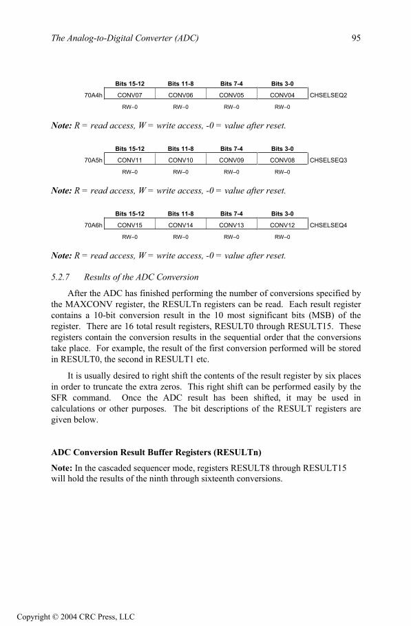
The Analog-to-Digital Converter (ADC) 95
Bits 15-12 Bits 11-8 Bits 7-4 Bits 3-0
70A4h CONV07 CONV06 CONV05 CONV04 CHSELSEQ2
RW–0 RW–0 RW–0 RW–0
Note: R = read access, W = write access, -0 = value after reset.
Bits 15-12 Bits 11-8 Bits 7-4 Bits 3-0
70A5h CONV11 CONV10 CONV09 CONV08 CHSELSEQ3
RW–0 RW–0 RW–0 RW–0
Note: R = read access, W = write access, -0 = value after reset.
Bits 15-12 Bits 11-8 Bits 7-4 Bits 3-0
70A6h CONV15 CONV14 CONV13 CONV12 CHSELSEQ4
RW–0 RW–0 RW–0 RW–0
Note: R = read access, W = write access, -0 = value after reset.
5.2.7 Results of the ADC Conversion
After the ADC has finished performing the number of conversions specified bythe MAXCONV register, the RESULTn registers can be read. Each result registercontains a 10-bit conversion result in the 10 most significant bits (MSB) of theregister. There are 16 total result registers, RESULT0 through RESULT15. Theseregisters contain the conversion results in the sequential order that the conversionstake place. For example, the result of the first conversion performed will be storedin RESULT0, the second in RESULT1 etc.
It is usually desired to right shift the contents of the result register by six placesin order to truncate the extra zeros. This right shift can be performed easily by theSFR command. Once the ADC result has been shifted, it may be used incalculations or other purposes. The bit descriptions of the RESULT registers aregiven below.
ADC Conversion Result Buffer Registers (RESULTn)
Note: In the cascaded sequencer mode, registers RESULT8 through RESULT15will hold the results of the ninth through sixteenth conversions.
Copyright © 2004 CRC Press, LLC

The Analog-to-Digital Converter (ADC)96
15 14 13 12 11 10 9 8
D9 D8 D7 D6 D5 D4 D3 D2
7 6 5 4 3 2 1 0
D1 D0 0 0 0 0 0 0
Notes:1) Buffer addresses = 70A8h to 70B7h (i.e., 16 registers)2) The 10-bit conversion result (D9–D0) is left-justified
5.2.8 The Auto-Sequence Status Register
The Auto-Sequence Status Register contains information on the current state ofthe sequencer when running conversions. Its bits can be polled (read) to determine,for example, if the sequencer is near or closer to the end number of conversions.
Auto-sequence Status Register (AUTO_SEQ_SR) — Address 70A7h
15-12 11 10 9 8
Reserved SEQCNTR 3
SEQCNTR 2
SEQCNTR 1
SEQCNTR 0
R–x R–0 R–0 R–0 R–0
7 6 5 4 3 2 1 0
Reserved SEQ2–State2
SEQ2–State1
SEQ2–State0
SEQ1–State3
SEQ1–State2
SEQ1–State1
SEQ1–State0
R–x R–0 R–0 R–0 R–0 R–0 R–0 R–0
Note: R = read access, x = undefined, -0 = value after reset.
Bits 15–12 Reserved
Bits 11–8 SEQ CNTR 3 – SEQ CNTR 0. Sequencing counter status bits
The SEQ CNTR n 4-bit status field is used by SEQ1, SEQ2, andthe cascaded sequencer. SEQ2 is irrelevant in cascaded mode.
At the start of an auto-sequenced session, SEQ CNTR n is loaded with thevalue from MAX CONVn. The SEQ CNTR n bits can be read at any time duringthe countdown process to check the status of the sequencer. This value, togetherwith the SEQ1 and SEQ2 busy bits, uniquely identifies the progress or state of theactive sequencer at any point in time.
Copyright © 2004 CRC Press, LLC

The Analog-to-Digital Converter (ADC) 97
SEQ CNTR n (read only) Number of conversions remaining
0000 1
0001 2
0010 3
0011 4
0100 5
0101 6
0110 7
0111 8
1000 9
1001 10
1010 11
1011 12
1100 13
1101 14
1110 15
1111 16
Bit 7 Reserved
Bits 6–4 SEQ2-State2 through SEQ2-State0
Reflects the state of SEQ2 sequencer at any point of time. If needbe, user can poll these bits to read interim results before an EOS.SEQ2 is irrelevant in cascaded mode.
Bits 3–0 SEQ1-State3 through SEQ1-State0
Reflects the state of SEQ1 sequencer at any point of time. If needbe, user can poll these bits to read interim results before an EOS.
Copyright © 2004 CRC Press, LLC

The Analog-to-Digital Converter (ADC)98
ADC Register Addresses Summary (Mapped in Data Memory)
Address Register Name
70A0h ADCTRL1 ADC control register 1
70A1h ADCTRL2 ADC control register 2
70A2h MAXCONV Maximum conversion channels register
70A3h CHSELSEQ1 Channel select sequencing control register 1
70A4h CHSELSEQ2 Channel select sequencing control register 2
70A5h CHSELSEQ3 Channel select sequencing control register 3
70A6h CHSELSEQ4 Channel select sequencing control register 4
70A7h AUTO_SEQ_SR Autosequence status register
70A8h RESULT0 Conversion result buffer register 0
70A9h RESULT1 Conversion result buffer register 1
70AAh RESULT2 Conversion result buffer register 2
70ABh RESULT3 Conversion result buffer register 3
70ACh RESULT4 Conversion result buffer register 4
70ADh RESULT5 Conversion result buffer register 5
70AEh RESULT6 Conversion result buffer register 6
70AFh RESULT7 Conversion result buffer register 7
70B0h RESULT8 Conversion result buffer register 8
70B1h RESULT9 Conversion result buffer register 9
70B2h RESULT10 Conversion result buffer register 10
70B3h RESULT11 Conversion result buffer register 11
70B4h RESULT12 Conversion result buffer register 12
70B5h RESULT13 Conversion result buffer register 13
70B6h RESULT14 Conversion result buffer register 14
70B7h RESULT15 Conversion result buffer register 15
70B8h CALIBRATION Calibration result, used to correct subsequent conversions
5.3 Analog to Digital Converter Usage Exercise
The purpose of this exercise is to familiarize the reader with the practical usageof the ADC. As stated earlier, the ADC on the LF2407 produces a 10-bit binarynumber which represents the voltage of the sampled analog signal.
This 10-bit number is stored in a 16-bit register “RESULTn” n=0..15. Whenreading from the register, the least significant 6 bits (bits 0-5) need to bedisregarded because the 10 ADC result bits are bits 15-6. This can be done with therepeat command and SFR command.
For example, after the initial value is loaded into the accumulator:RPT #5 SFR ; the accumulator will be shifted right 6 (RPT+1) times
Copyright © 2004 CRC Press, LLC

The Analog-to-Digital Converter (ADC) 99
Create an assembly source file and project file called “lab5”which:
a. Turns on the ADC clock in SCSR1 during the general initialization.b. Puts the ADC in Reset.c. Configures the ADC for Cascaded Mode; Continuous Mode = OFF;
brings ADC out of Reset mode.d. Sets maximum conversions to one and selects channel 0 for
conversion.e. Triggers a SOC via BIT 13 in ADCTRL2.f. Checks if the ADC is finished via BIT 12 in ADCCTRL2. g. If the ADC is finished with the conversion, the accumulator is loaded
with the value in RESULT0 (the ADC conversion).h. Continuously loops in an endless loop, i.e., does nothing.
1. Run the code on the LF2407 EVM with a 1.5V battery connected tochannel 0 of the ADC and analog ground.
2. Record the value from the accumulator (the accumulator has been loadedwith the value from the first ADC RESULT register). The value should beapproximately half of the full voltage value 0x3FFF or approximately“1FF” = (1.5V).
3. Modify the program to output the result data from address 60h to DACchannel 1 on the LF2407 EVM. The DAC onboard is a 12-bit DAC, so inorder to get the correct voltage output, left shift the accumulator (ADCdata) two places to account for the extra two least significant bits. Also,the EVM DAC has a voltage reference of 5V rather then 3.3V like theADC. This will cause a voltage slightly higher than what the ADCsampled to be outputted on the DAC channel. For this academic exercise, this can be ignored because the voltage difference is somewhat small.When writing to the DAC Channel 1, the data must first be written to IO space address 0000h. Then, in order for the data to actually be “sent out”on the DAC, the IO space address 0004h must be written to. It does notmatter what value is written to IO address 0004h, just as long as it is written to.
4. The data will then be sent from the buffers to the DAC outputs. (See theOUT command and the Spectrum Digital LF2407 EVM manual for moreinformation on programming the on-board DAC.)
5. Rebuild the project, reset the DSP, and run the new code.6. Measure the voltage output of the DAC. It should reflect the ADC input
voltage.7. Modify the program to have the ADC continuously sample and
continuously output the sampled data on the DAC.8. Rebuild the program, reset, and run the DSP.
This concludes the ADC usage exercise.
Copyright © 2004 CRC Press, LLC

Chapter 6
THE EVENT MANAGERS (EVA, EVB)
This chapter explains the features and operation of the LF2407 Event Managers(EV1, EV2). There are two identical event managers on board the LF2407 DSP.All control orientated features of the LF2407 are centered in the EV. The eventmanager peripheral is made up of components such as timers and pulse widthmodulation (PWM) generators. We start with a brief overview of the EV withoutgetting into too much detail. Since the EV consists of several sub-components, wediscuss in detail the operation and functionality of each sub-component separatelyin subsequent sections.
6.1 Overview of the Event Manager (EV)
We start with the EV by reviewing the multiple functional modules of theperipheral. The two EVs (EVA/B) are identical to one another in terms of functionality and register/bit definition, but have different register names andaddresses. Since both EV1 and EV2 are identical, only the functionality of EV1will be explained.
Each EV module in the LF2407 contains the following sub-components:
Interrupt logic Two general-purpose (GP) timers Three compare units PWM circuits that include space vector PWM circuits, dead-band
generation units, and output logic Three Capture Units Quadrature encoder pulse (QEP) circuit
Figure 6.1 shows a block diagram of the EVA module. Similarly, Fig. 6.2illustrates the block diagram of EVB.
Like all peripherals, the EV registers occupy a range of 16-bit memoryaddresses in data memory space. Most of these registers are programmable control and data registers, but read-only status registers are also present. EVA registers arelocated in the data memory range 7400h to 7431h. EVB registers are located in therange of 7500h to 7531h. Some of the EV memory allocation range is for use bythe DSP only. These undefined registers and undefined bits of EV registers will justread zero when read by user software. Writes also have no effect on these registers.As a general rule, one should not write to reserved or illegal addresses in order to avoid an illegal address non-maskable interrupt (NMI) from occurring.
101
Copyright © 2004 CRC Press, LLC

The Event Managers (EVA, EVB)102
Outputlogic
PWM1
PWM6
T2CMP/T2PWM
T1CMP/T1PWM
1616
16
16
16
16
16
16
16
16
16
3 3 3
ADC start ofconversion
QEPcircuit
ClockDIR
16
16
2 CAP1/QEP1CAP2/QEP2CAP3
TDIRA
TCLKINA
CLKOUT
T1CON[8,9,10]T1CON[4,5]
T2CON[8,9,10]T2CON[4,5]
CLKOUTTCLKINA
TDIRA
Outputlogic
Deadbandunits
SVPWMstate
machine
22
CAPCONA[14,13]
Capture units
GP timer 1
Full compareunits
GP timer 2compare
GP timer 2
EV control registersand control logic
GP timer 1compare
Outputlogic
Databus ADDR bus Reset INT1,2,3,4 Clock
240xA DSP core
MUX
Prescaler
Prescaler
Figure 6.1 Event Manager A (EVA) block diagram. (Courtesy of TexasInstruments)
6.2 Event Manager Interrupts
The interrupt system in the EV will be discussed first because each of the sub-modules of the EVs have interrupt flags. The EV interrupt sub-system is slightlydifferent from that of the main interrupt system. Each EV has its own “local”interrupt sub-system which includes its own interrupt mask and flag registers. Afterthe EV interrupts pass through the sub-system, they flow into the PIE just like anyother interrupt on the LF2407. The EV interrupts are arranged into three groups(A, B, C). Each group (A,B,C) has its own mask and flag register and is assigned to
Copyright © 2004 CRC Press, LLC

The Event Managers (EVA, EVB) 103
a particular CPU interrupt priority level at the PIE. EV interrupts happen to be onlyat the INT2, INT3, and INT4 CPU priority levels.
Outputlogic
PWM7
PWM12
T4CMP/T4PWM
T3CMP/T3PWM
1616
16
16
16
16
16
16
16
16
16
3 3 3
ADC start ofconversion
QEPcircuit
ClockDIR
16
16
2 CAP4/QEP3CAP5/QEP4CAP6
TDIRB
TCLKINB
CLKOUT
T3CON[8,9,10]T3CON[4,5]
T4CON[8,9,10]T4CON[4,5]
CLKOUTTCLKINB
TDIRB
Outputlogic
Deadbandunits
SVPWMstate
machine
22
CAPCONB[14,13]
Capture units
GP timer 3
Full compareunits
GP timer 4compare
GP timer 4
EV control registersand control logic
GP timer 3compare
Outputlogic
Databus ADDR bus Reset INT1,2,3,4 Clock
240xA DSP core
MUX
Prescaler
Prescaler
Figure 6.2 Event Manager B (EVB) block diagram. (Courtesy of TexasInstruments)
The following are the sequential steps for interrupt response within the EV:
1. Interrupt source. When an EV interrupt condition occurs, the respectiveflag bits in registers EVxIFRA, EVxIFRB, or EVxIFRC (x = A or B) areset. As with other peripheral level flags, once set, these flags remain setuntil explicitly cleared by the software. In other words, you must clear
Copyright © 2004 CRC Press, LLC

The Event Managers (EVA, EVB)104
theses flags “manually” through your software in order for future interruptsto be recognized.
2. Interrupt enable. The EV interrupts can be individually enabled ordisabled by the EV interrupt mask registers EVxIMRA, EVxIMRB, andEVxIMRC (x being either EV = A or B ). To enable (unmask) an interrupt,the user must set the corresponding bit to “1”. To disable (mask) the interrupt, clear the corresponding bit to “0”. From now on, the interrupt ishandled like other peripheral interrupts as discussed earlier in the text.
3. PIE request. If both interrupt flag bits and interrupt mask bits are set, thenthe interrupt request is passed to the PIE module. As with any otherperipheral interrupts, the PIE module will send the CPU a request for aCPU level interrupt of the appropriate priority level based on the priority ofthe received interrupts.
4. CPU response. On receiving a CPU level interrupt request, the respectivebit in the CPU interrupt flag register (IFR) will be set. If the correspondinginterrupt mask register (IMR) bit is set and INTM bit is cleared, then the CPU recognizes the interrupt and issues an acknowledgement to the PIE module. Following this, the CPU finishes executing the current instructionand branches to the interrupt service routine via the interrupt vector. Atthis time, the respective IFR bit will be cleared and the INTM bit will beset disabling further interrupt recognition. The interrupt vector contains a branch instruction for the interrupt service routine. From here, the user software controls the interrupt servicing.
5. Interrupt software. The interrupt software can include two levels ofresponse.
a. GISR: The General Interrupt Service Routine (GISR) should do anycontext save and read the PIVR register to decide which specificinterrupt occurred. Information on PIVR values and theircorresponding interrupts can be found in Tables 6.1 and 6.2. Since thePIVR value for each interrupt is unique, it can be used to branch to theinterrupt service routine specific to this interrupt condition.
b. SISR: The Specific Interrupt Service Routine (SISR) level willnormally reside as a sub-section of the GISR. After executing theinterrupt specific service code, the routine should clear the interruptflag in the EVxIFRA, EVxIFRB, or EVxIFRC that caused the servicedinterrupt. Code will return the CPU to the pre-interrupt task after enabling the CPU’s global interrupt bit INTM (clear INTM bit).
Copyright © 2004 CRC Press, LLC

The Event Managers (EVA, EVB) 105
EVA Interrupts
Table 6.1 EVA Interrupts and Corresponding PIVR Values
Group Interrupt Priority withingroup
Vector(ID)
Description/Source INT
PDPINTA 1 (highest) 0020h Power Drive Protection Interrupt A 1A CMP1INT 2 0021h Compare Unit 1 compare interrupt 2
CMP2INT 3 0022h Compare Unit 2 compare interrupt 2CMP3INT 4 0023h Compare Unit 3 compare interrupt 2T1PINT 5 0027h GP Timer 1 period interrupt 2T1CINT 6 0028h GP Timer 1 compare interrupt 2T1UFINT 7 0029h GP Timer 1 underflow interrupt 2T1OFINT 8 (lowest) 002Ah GP Timer 1 overflow interrupt 2
B T2PINT 1 (highest) 002Bh GP Timer 2 period interrupt 3T2CINT 2 002Ch GP Timer 2 compare interrupt 3T2UFINT 3 002Dh GP Timer 2 underflow interrupt 3T2OFINT 4 002Eh GP Timer 2 overflow interrupt 3
C CAP1INT 1 (highest) 0033h Capture Unit 1 interrupt 4CAP2INT 2 0034h Capture Unit 2 interrupt 4CAP3INT 3 0035h Capture Unit 3 interrupt 4
EVB Interrupts
Table 6.2 EVB Interrupts and Corresponding PIVR Values
Group Interrupt Priority withingroup
Vector(ID)
Description/Source INT
PDPINTB 1 (highest) 0019h Power Drive Protection Interrupt B 1A CMP4INT 2 0024h Compare Unit 4 compare interrupt 2
CMP5INT 3 0025h Compare Unit 5 compare interrupt 2CMP6INT 4 0026h Compare Unit 6 compare interrupt 2T3PINT 5 002Fh GP Timer 3 period interrupt 2T3CINT 6 0030h GP Timer 3 compare interrupt 2T3UFINT 7 0031h GP Timer 3 underflow interrupt 2T3OFINT 8 (lowest) 0032h GP Timer 3 overflow interrupt 2
B T4PINT 1 (highest) 0039h GP Timer 4 period interrupt 3T4CINT 2 003Ah GP Timer 4 compare interrupt 3T4UFINT 3 003Bh GP Timer 4 underflow interrupt 3T4OFINT 4 003Ch GP Timer 4 overflow interrupt 3
C CAP4INT 1 (highest) 0036h Capture Unit 4 interrupt 4CAP5INT 2 0037h Capture Unit 5 interrupt 4CAP6INT 3 0038h Capture Unit 6 interrupt 4
Copyright © 2004 CRC Press, LLC

The Event Managers (EVA, EVB)106
EVA Interrupt Flag Register A (EVAIFRA) — Address 742Fh
15-11 10 9 8
Reserved T1OFINTFLAG
T1UFINTFLAG
T1CINTFLAG
R–0 RW1C–0 RW1C–0 RW1C–0
7 6-4 3 2 1 0
T1PINTFLAG
Reserved CMP3INTFLAG
CMP2INTFLAG
CMP1INTFLAG
PDPINTAFLAG
RW1C–0 R–0 RW1C–0 RW1C–0 RW1C–0 RW1C–0
Note: R = read access, W1C = write 1 to clear, -0 = value after reset.
Bits 15–11 Reserved. Reads return zero; writes have no effect.
Bit 10 T1OFINT FLAG. GP Timer 1 overflow interrupt.Read: 0 Flag is reset
1 Flag is setWrite: 0 No effect
1 Resets flag
Bit 9 T1UFINT FLAG. GP Timer 1 underflow interrupt.Read: 0 Flag is reset
1 Flag is setWrite: 0 No effect
1 Resets flag
Bit 8 T1CINT FLAG. GP Timer 1 compare interrupt.Read: 0 Flag is reset
1 Flag is setWrite: 0 No effect
1 Resets flag
Bit 7 T1PINT FLAG. GP Timer 1 period interrupt.Read: 0 Flag is reset
1 Flag is setWrite: 0 No effect
1 Resets flag
Bits 6–4 Reserved. Reads return zero; writes have no effect.
Bit 3 CMP3INT FLAG. Compare 3 interrupt.Read: 0 Flag is reset
1 Flag is setWrite: 0 No effect
1 Resets flag
Copyright © 2004 CRC Press, LLC

The Event Managers (EVA, EVB) 107
Bit 2 CMP2INT FLAG. Compare 2 interrupt.Read: 0 Flag is reset
1 Flag is setWrite: 0 No effect
1 Resets flag
Bit 1 CMP1INT FLAG. Compare 1 interrupt.Read: 0 Flag is reset
1 Flag is setWrite: 0 No effect
1 Resets flag
Bit 0 PDPINTA FLAG. Power drive protection interrupt.Read: 0 Flag is reset
1 Flag is setWrite: 0 No effect
1 Resets flag
EVA Interrupt Flag Register B (EVAIFRB) — Address 7430h
15-4 3 2 1 0
Reserved T2OFINTFLAG
T2UFINTFLAG
T2CINTFLAG
T2PINTFLAG
R–0 RW1C–0 RW1C–0 RW1C–0 RW1C–0
Note: R = read access, W1C = write 1 to clear, -0 = value after reset.
Bits 15–4 Reserved. Reads return zero; writes have no effect.
Bit 3 T2OFINT FLAG. GP Timer 2 overflow interrupt.Read: 0 Flag is reset
1 Flag is setWrite: 0 No effect
1 Resets flag
Bit 2 T2UFINT FLAG. GP Timer 2 underflow interrupt.Read: 0 Flag is reset
1 Flag is setWrite: 0 No effect
1 Resets flag
Bit 1 T2CINT FLAG. GP Timer 2 compare interrupt.Read: 0 Flag is reset
1 Flag is setWrite: 0 No effect
1 Resets flag
Copyright © 2004 CRC Press, LLC

The Event Managers (EVA, EVB)108
Bit 0 T2PINT FLAG. GP Timer 2 period interrupt.Read: 0 Flag is reset
1 Flag is setWrite: 0 No effect
1 Resets flag
EVA Interrupt Flag Register C (EVAIFRC) — Address 7431h
15-3 2 1 0
Reserved CAP3INTFLAG
CAP2INTFLAG
CAP1INTFLAG
R–0 RW1C–0 RW1C–0 RW1C–0
Note: R = read access, W1C = write 1 to clear, -0 = value after reset.
Bits 15–3 Reserved. Reads return zero; writes have no effect.
Bit 2 CAP3INT FLAG. Capture 3 interrupt.Read: 0 Flag is reset
1 Flag is setWrite: 0 No effect
1 Resets flag
Bit 1 CAP2INT FLAG. Capture 2 interrupt.Read: 0 Flag is reset
1 Flag is setWrite: 0 No effect
1 Resets flag
Bit 0 CAP1INT FLAG. Capture 1 interrupt.Read: 0 Flag is reset
1 Flag is setWrite: 0 No effect
1 Resets flag
EVA Interrupt Mask Register A (EVAIMRA) — Address 742Ch
15-11 10 9 8
Reserved T1OFINTENABLE
T1UFINTENABLE
T1CINTENABLE
R–0 RW–0 RW–0 RW–0
7 6-4 3 2 1 0
T1PINTENABLE
Reserved CMP3INTENABLE
CMP2INTENABLE
CMP1INTENABLE
PDPINTAENABLE
RW–0 R–0 RW–0 RW–0 RW–0 RW–1
Note: R = read access, W = write access, value following dash (–) = value after reset.
Copyright © 2004 CRC Press, LLC

The Event Managers (EVA, EVB) 109
Bits 15–11 Reserved. Reads return zero; writes have no effect.
Bit 10 T1OFINT ENABLE0 Disable1 Enable
Bit 9 T1UFINT ENABLE0 Disable1 Enable
Bit 8 T1CINT ENABLE0 Disable1 Enable
Bit 7 T1PINT ENABLE 0 Disable1 Enable
Bits 6–4 Reserved. Reads return zero; writes have no effect.
Bit 3 CMP3INT ENABLE0 Disable1 Enable
Bit 2 CMP2INT ENABLE0 Disable1 Enable
Bit 1 CMP1INT ENABLE0 Disable1 Enable
Bit 0 PDPINTA ENABLE. This is enabled (set to 1) following reset.0 Disable1 Enable
EVA Interrupt Mask Register B (EVAIMRB) — Address 742Dh
15-4 3 2 1 0
Reserved T2OFINTENABLE
T2UFINTENABLE
T2CINTENABLE
T2PINTENABLE
R–0 RW–0 RW–0 RW–0 RW–0
Note: R = read access, W = write access, -0 = value after reset.
Bits 15–4 Reserved. Reads return zero; writes have no effect.
Bit 3 T2OFINT ENABLE0 Disable1 Enable
Copyright © 2004 CRC Press, LLC

The Event Managers (EVA, EVB)110
Bit 2 T2UFINT ENABLE0 Disable1 Enable
Bit 1 T2CINT ENABLE0 Disable1 Enable
Bit 0 T2PINT ENABLE 0 Disable1 Enable
EVA Interrupt Mask Register C (EVAIMRC) — Address 742Eh
15-3 2 1 0
Reserved CAP3INTENABLE
CAP2INTENABLE
CAP1INTENABLE
R–0 RW–0 RW–0 RW–0
Note: R = read access, W = write access, -0 = value after reset.Bits 15–3 Reserved. Reads return zero; writes have no effect.
Bit 2 CAP3INT ENABLE0 Disable1 Enable
Bit 1 CAP2INT ENABLE0 Disable1 Enable
Bit 0 CAP1INT ENABLE0 Disable1 Enable
EVB Interrupt Flag Register A (EVBIFRA) — Address 752Fh
15-11 10 9 8
Reserved T3OFINTFLAG
T3UFINTFLAG
T3CINTFLAG
R–0 RW1C–0 RW1C–0 RW1C–0
7 6-4 3 2 1 0
T3PINTFLAG
Reserved CMP6INTFLAG
CMP5INTFLAG
CMP4INTFLAG
PDPINTBFLAG
RW1C–0 R–0 RW1C–0 RW1C–0 RW1C–0 RW1C–0
Note: R = read access, W1C = write 1 to clear, -0 = value after reset.
Copyright © 2004 CRC Press, LLC

The Event Managers (EVA, EVB) 111
Bits 15–11 Reserved. Reads return zero; writes have no effect.
Bit 10 T3OFINT FLAG. GP Timer 3 overflow interrupt.Read: 0 Flag is reset
1 Flag is setWrite: 0 No effect
1 Resets flag
Bit 9 T3UFINT FLAG. GP Timer 3 underflow interrupt.Read: 0 Flag is reset
1 Flag is setWrite: 0 No effect
1 Resets flag
Bit 8 T3CINT FLAG. GP Timer 3 compare interrupt.Read: 0 Flag is reset
1 Flag is setWrite: 0 No effect
1 Resets flagBit 7 T3PINT FLAG. GP Timer 3 period interrupt.
Read: 0 Flag is reset 1 Flag is set
Write: 0 No effect1 Resets flag
Bits 6–4 Reserved. Reads return zero; writes have no effect.
Bit 3 CMP6INT FLAG. Compare 6 interrupt.Read: 0 Flag is reset
1 Flag is setWrite: 0 No effect
1 Resets flag
Bit 2 CMP5INT FLAG. Compare 5 interrupt.Read: 0 Flag is reset
1 Flag is setWrite: 0 No effect
1 Resets flag
Bit 1 CMP4INT FLAG. Compare 4 interrupt.Read: 0 Flag is reset
1 Flag is setWrite: 0 No effect
1 Resets flag
Copyright © 2004 CRC Press, LLC

The Event Managers (EVA, EVB)112
Bit 0 PDPINTB FLAG. Power drive protection interrupt.Read: 0 Flag is reset
1 Flag is setWrite: 0 No effect
1 Resets flag
EVB Interrupt Flag Register B (EVBIFRB) — Address 7530h
15-4 3 2 1 0
Reserved T4OFINTFLAG
T4UFINTFLAG
T4CINTFLAG
T4PINTFLAG
R–0 RW1C–0 RW1C–0 RW1C–0 RW1C–0
Note: R = read access, W1C = write 1 to clear, -0 = value after reset.
Bits 15–4 Reserved. Reads return zero; writes have no effect.
Bit 3 T4OFINT FLAG. GP Timer 4 overflow interrupt.Read: 0 Flag is reset
1 Flag is setWrite: 0 No effect
1 Resets flag
Bit 2 T4UFINT FLAG. GP Timer 4 underflow interrupt.Read: 0 Flag is reset
1 Flag is setWrite: 0 No effect
1 Resets flag
Bit 1 T4CINT FLAG. GP Timer 4 compare interrupt.Read: 0 Flag is reset
1 Flag is setWrite: 0 No effect
1 Resets flag
Bit 0 T4PINT FLAG. GP Timer 4 period interrupt.Read: 0 Flag is reset
1 Flag is setWrite: 0 No effect
1 Resets flag
Copyright © 2004 CRC Press, LLC

The Event Managers (EVA, EVB) 113
EVB Interrupt Flag Register C (EVBIFRC) — Address 7531h
15-3 2 1 0
Reserved CAP6INTFLAG
CAP5INTFLAG
CAP4INTFLAG
R–0 RW1C–0 RW1C–0 RW1C–0
Note: R = read access, W1C = write 1 to clear, -0 = value after reset.
Bits 15–3 Reserved. Reads return zero; writes have no effect.
Bit 2 CAP6INT FLAG. Capture 6 interrupt.Read: 0 Flag is reset
1 Flag is setWrite: 0 No effect
1 Resets flag
Bit 1 CAP5INT FLAG. Capture 5 interrupt.Read: 0 Flag is reset
1 Flag is setWrite: 0 No effect
1 Resets flag
Bit 0 CAP4INT FLAG. Capture 4 interrupt.Read: 0 Flag is reset
1 Flag is setWrite: 0 No effect
1 Resets flag
EVB Interrupt Mask Register A (EVBIMRA) — Address 752Ch
15-11 10 9 8
Reserved T3OFINTENABLE
T3UFINTENABLE
T3CINTENABLE
R–0 RW–0 RW–0 RW–0
7 6-4 3 2 1 0
T3PINTENABLE
Reserved CMP6INTENABLE
CMP5INTENABLE
CMP4INTENABLE
PDPINTBENABLE
RW–0 R–0 RW–0 RW–0 RW–0 RW–1
Note: R = read access, W = write access, -n = value after reset.
Bits 15–11 Reserved. Reads return zero; writes have no effect.
Copyright © 2004 CRC Press, LLC

The Event Managers (EVA, EVB)114
Bit 10 T3OFINT ENABLE0 Disable1 Enable
Bit 9 T3UFINT ENABLE0 Disable1 Enable
Bit 8 T3CINT ENABLE0 Disable1 Enable
Bit 7 T3PINT ENABLE 0 Disable1 Enable
Bits 6–4 Reserved. Reads return zero; writes have no effect.
Bit 3 CMP6INT ENABLE0 Disable1 Enable
Bit 2 CMP5INT ENABLE0 Disable1 Enable
Bit 1 CMP4INT ENABLE0 Disable1 Enable
Bit 0 PDPINTB ENABLE. This is enabled (set to 1) following reset.0 Disable1 Enable
EVB Interrupt Mask Register B (EVBIMRB) — Address 752Dh
15-4 3 2 1 0
Reserved T4OFINTENABLE
T4UFINTENABLE
T4CINTENABLE
T4PINTENABLE
R–0 RW–0 RW–0 RW–0 RW–0
Note: R = read access, W = write access, -0 = value after reset.
Copyright © 2004 CRC Press, LLC

The Event Managers (EVA, EVB) 115
Bits 15–4 Reserved. Reads return zero; writes have no effect.
Bit 3 T4OFINT ENABLE0 Disable1 Enable
Bit 2 T4UFINT ENABLE0 Disable1 Enable
Bit 1 T4CINT ENABLE0 Disable1 Enable
Bit 0 T4PINT ENABLE 0 Disable1 Enable
EVB Interrupt Mask Register C (EVBIMRC) — Address 752Eh
15-3 2 1 0
Reserved CAP6INTENABLE
CAP5INTENABLE
CAP4INTENABLE
R–0 RW–0 RW–0 RW–0
Note: R = read access, W = write access, -0 = value after reset.
Bits 15–3 Reserved. Reads return zero; writes have no effect.
Bit 2 CAP6INT ENABLE0 Disable1 Enable
Bit 1 CAP5INT ENABLE0 Disable1 Enable
Bit 0 CAP4INT ENABLE0 Disable1 Enable
6.3 General Purpose (GP) Timers
A General Purpose (GP) timer is simply a 16-bit counter, which may beconfigured to count up, down, or continuously up and down. There are two GP Timers in each EV: Timer1 and Timer2 for EVA and Timer3 and Timer4 for EVB.
Copyright © 2004 CRC Press, LLC

The Event Managers (EVA, EVB)116
All timers use the CPU clock as a general timing reference, but each individualtimer may use a “pre-scaled” or frequency reduced time base which is specified in each timer’s control register.
A GP Timer may also be configured to generate an interrupt or trigger anotherperipheral on certain events such as a timer overflow (timer reached period value),underflow (timer reached zero), or compare (timer value reached compare value).Some examples of uses for the GP Timers include: setting the sampling period forthe ADC by triggering the start of conversion; or providing the switching period forthe generation of a PWM signal.
Figure 6.3 shows a block diagram of a GP Timer. There are two cases thatapply to Fig. 6.3:
1. When “x” = 2, “y” = 1 and “n” = 22. When “x” = 4, “y” = 3 and “n” = 4
TxPRperiod register
(shadowed)
TyPR period register(shadowed)
TxCMPRcompareregister
(shadowed)
Comparelogic
MUX
Symm/asymwaveformgenerator
GPTCONA/BGP timer controlregister
Outputlogic
TxCNT GPtimer counter
Controllogic
TxCON GPTxcontrol register
Interrupt flags
TxPWM
ADC start ofconversion
TCLKINA/BTDIRA/B
InternalCPU clock
TnCON[0]
Figure 6.3 General purpose timer configuration diagram.
Copyright © 2004 CRC Press, LLC

The Event Managers (EVA, EVB) 117
Each GP Timer consists of the following components:
One readable and writeable (RW) 16-bit up and up/down counter registerTxCNT (x = 1, 2, 3, 4). This register holds the current count value andincrements or decrements depending on the direction of counting16-bit timer compare register, TxCMPR (x = 1, 2, 3, 4)16-bit timer period register, TxPR (x = 1, 2, 3, 4)16-bit individual timer control register, TxCON (x = 1, 2, 3, 4)Programmable input clock divider (pre-scaler) applicable to both internaland external clock inputs One GP Timer compare output pin, TxCMP (x = 1, 2, 3, 4)Interrupt logic
6.3.1 GP Timer Inputs and Outputs
Each GP Timer has the following inputs:
Clock Reference Inputs: (1) The internal device (CPU) clock and (2)external clock, TCLKINA/B, that has a maximum frequency of one-fourththat of the device clockDirection input, TDIRA/B, when a GP Timer is in directional up/down-counting modeReset signal, RESET
The source of the GP Timer clock can be the internal CPU clock signal or theexternal clock input, TCLKINA/B. The frequency of the external clock must be lessthan or equal to one-fourth of that of the device clock. GP Timer 2 (EVA) and GPTimer 4 (EVB) can be used with the QEP circuits in directional up-/down-countingmode. In this case, the QEP circuits provide both the clock and direction inputs tothe timer. A wide range of prescale factors are provided for the clock input to each GP Timer.
The QEP circuit, when selected, can generate the input clock and countingdirection for GP Timer 2/4 in the directional up-/down-counting mode. A QEPsignal may come from a rotary encoder which is attached to a motor shaft to providespeed/direction feedback. Via the QEP circuitry, it controls the clock input anddirection of Timer 2/4. From this, the speed of the motor can be determined fromthe counting speed; the direction of count reflects the rotation direction. The QEPinput clock cannot be scaled by GP Timer prescaler circuits (the prescaler of theselected GP Timer has no effect if the QEP circuit is selected as the clock source).Furthermore, the frequency of the clock generated by the QEP circuits is four timesthat of the frequency of each QEP input channel because the rising and falling edgesof both QEP input channels are counted by the selected timer. In other words, the frequency of the incoming QEP signal must be less than or equal to one-fourth ofthat of the CPU clock.
Now that the inputs to the GP Timers have been discussed, we will next discussthe outputs associated with each GP Timer. Outputs are either connected to a data
Copyright © 2004 CRC Press, LLC
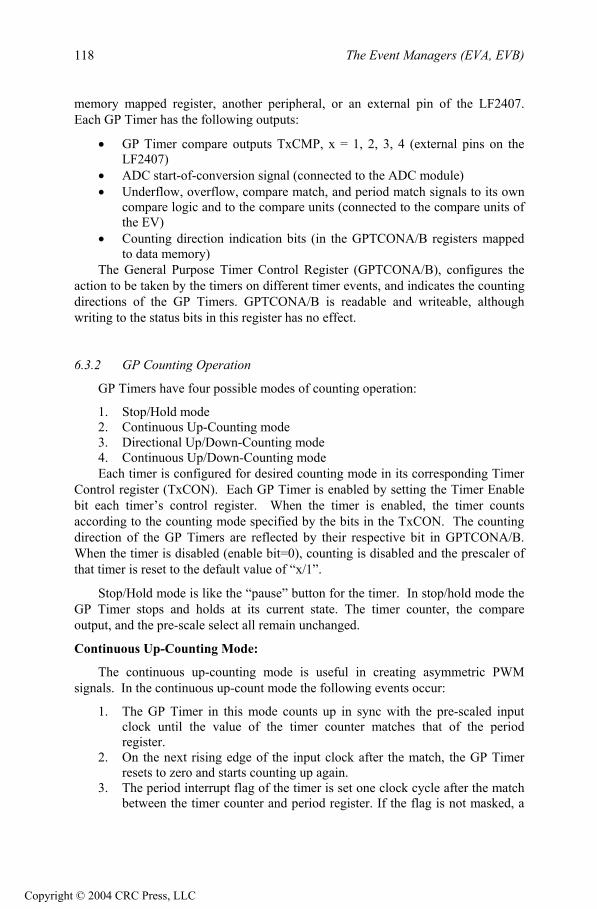
The Event Managers (EVA, EVB)118
memory mapped register, another peripheral, or an external pin of the LF2407.Each GP Timer has the following outputs:
GP Timer compare outputs TxCMP, x = 1, 2, 3, 4 (external pins on theLF2407)ADC start-of-conversion signal (connected to the ADC module)Underflow, overflow, compare match, and period match signals to its owncompare logic and to the compare units (connected to the compare units of the EV) Counting direction indication bits (in the GPTCONA/B registers mappedto data memory)
The General Purpose Timer Control Register (GPTCONA/B), configures theaction to be taken by the timers on different timer events, and indicates the countingdirections of the GP Timers. GPTCONA/B is readable and writeable, althoughwriting to the status bits in this register has no effect.
6.3.2 GP Counting Operation
GP Timers have four possible modes of counting operation:
1. Stop/Hold mode2. Continuous Up-Counting mode3. Directional Up/Down-Counting mode4. Continuous Up/Down-Counting modeEach timer is configured for desired counting mode in its corresponding Timer
Control register (TxCON). Each GP Timer is enabled by setting the Timer Enablebit each timer’s control register. When the timer is enabled, the timer countsaccording to the counting mode specified by the bits in the TxCON. The countingdirection of the GP Timers are reflected by their respective bit in GPTCONA/B. When the timer is disabled (enable bit=0), counting is disabled and the prescaler ofthat timer is reset to the default value of “x/1”.
Stop/Hold mode is like the “pause” button for the timer. In stop/hold mode theGP Timer stops and holds at its current state. The timer counter, the compareoutput, and the pre-scale select all remain unchanged.
Continuous Up-Counting Mode:
The continuous up-counting mode is useful in creating asymmetric PWMsignals. In the continuous up-count mode the following events occur:
1. The GP Timer in this mode counts up in sync with the pre-scaled inputclock until the value of the timer counter matches that of the periodregister.
2. On the next rising edge of the input clock after the match, the GP Timerresets to zero and starts counting up again.
3. The period interrupt flag of the timer is set one clock cycle after the matchbetween the timer counter and period register. If the flag is not masked, a
Copyright © 2004 CRC Press, LLC
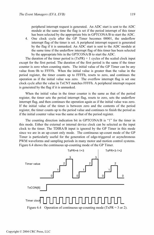
The Event Managers (EVA, EVB) 119
peripheral interrupt request is generated. An ADC start is sent to the ADCmodule at the same time the flag is set if the period interrupt of this timerhas been selected by the appropriate bits in GPTCONA/B to start the ADC.
4. One clock cycle after the GP Timer becomes 00001, the underflowinterrupt flag of the timer is set. A peripheral interrupt request is generatedby the flag if it is unmasked. An ADC start is sent to the ADC module atthe same time if the underflow interrupt flag of this timer has been selected by the appropriate bits in the GPTCONA/B to start the ADC.
The duration of the timer period is (TxPR) + 1 cycles of the scaled clock inputexcept for the first period. The duration of the first period is the same if the timercounter is zero when counting starts. The initial value of the GP Timer can be anyvalue from 0h to FFFFh. When the initial value is greater than the value in theperiod register, the timer counts up to FFFFh, resets to zero, and continues theoperation as if the initial value was zero. The overflow interrupt flag is set oneclock cycle after the value in TxCNT matches FFFFh. A peripheral interrupt requestis generated by the flag if it is unmasked.
When the initial value in the timer counter is the same as that of the periodregister, the timer sets the period interrupt flag, resets to zero, sets the underflowinterrupt flag, and then continues the operation again as if the initial value was zero.If the initial value of the timer is between zero and the contents of the periodregister, the timer counts up to the period value and continues to finish the period as if the initial counter value was the same as that of the period register.
The counting direction indication bit in GPTCONA/B is “1” for the timer inthis mode. Either the external or internal device clock can be selected as the input clock to the timer. The TDIRA/B input is ignored by the GP Timer in this modesince we are in an up-count only mode. The continuous up-count mode of the GPTimer is particularly useful for the generation of edge-triggered or asynchronousPWM waveforms and sampling periods in many motor and motion control systems.Figure 6.4 shows the continuous up-counting mode of the GP Timer.
TxPR=4-1=3 TxPR=3-1=2
3
2
1
0
3
2
1
0 0
2
1
0
Timer value
TxCON[6]
Timer clock
Figure 6.4 Operation of continuous up-counting mode (TxPR = 3 or 2).
Copyright © 2004 CRC Press, LLC

The Event Managers (EVA, EVB)120
Directional Up/Down-Counting Mode:
A GP Timer in directional up/down-counting mode counts either up or downaccording to the pre-scaled clock and TDIRA/B inputs. The input pin TDIRA/Bdetermines the direction of counting when the GP Timer is in directional up/down-counting mode. When TDIRA/B is high, upward counting is specified; whenTDIRA/B is low, downward counting is specified.
When the TDIRA/B pin is held high, the GP Timer will count up until it reaches the value of the period register. When the timer value equals that of itsperiod register the timer will reset to zero and start counting up to the period again.The initial value of the timer can be any value between 0000h to FFFFh. In the case that the initial value of the timer counter is greater than that of the period register,the timer would count up to FFFFh before resetting itself to zero and continuing thecounting operation. When TDIRA/B pin is held low, the GP Timer will count downfrom whatever initial value the counter was at until its count value becomes zero.When its count value becomes zero, the value of the period register is automaticallyloaded into the count value register and the timer begins counting down to zero.
In the directional up/down mode, the period, underflow, and overflow interruptflags, interrupts, and associated actions are generated on respective events in thesame manner as they are generated in the continuous up-counting mode. Thedirection of counting is indicated for the timer in this mode by the correspondingdirection indication bit in GPTCONA/B: 1 means counting up; 0 means countingdown. Either the external clock from the TCLKINA/B pin or the internal deviceclock can be used as the input clock for the timer in this mode. Figure 6.5 showsthe directional up-/down-counting mode of the GP Timers.
CLKTimer
TxCON[6
TDIRA/B
valueTimer
TxPR=3
12
3
01
2
3
21
0
32
10
6553565534
65533
0
Figure 6.5 GP timer directional up/down-counting mode: prescale factor 1 and
TxPR = 3A.
Additionally, the directional up-/down-counting mode of GP Timer 2 and 4 can also be used with the Quadrature Encoder Pulse (QEP) circuits in the EV module.While the QEP circuits are active, they provide both the counting clock anddirection for GP Timers 2 or 4.
Copyright © 2004 CRC Press, LLC
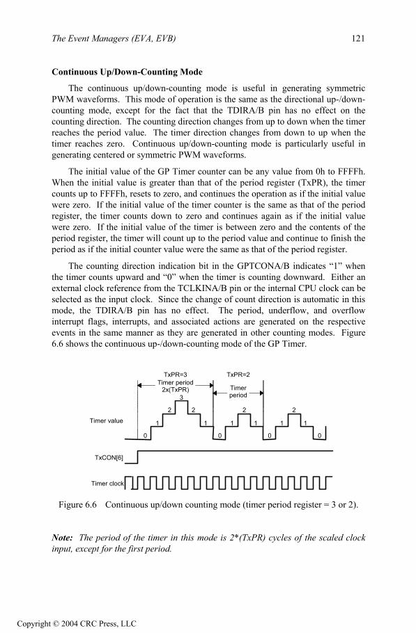
The Event Managers (EVA, EVB) 121
Continuous Up/Down-Counting Mode
The continuous up/down-counting mode is useful in generating symmetricPWM waveforms. This mode of operation is the same as the directional up-/down-counting mode, except for the fact that the TDIRA/B pin has no effect on thecounting direction. The counting direction changes from up to down when the timerreaches the period value. The timer direction changes from down to up when thetimer reaches zero. Continuous up/down-counting mode is particularly useful in generating centered or symmetric PWM waveforms.
The initial value of the GP Timer counter can be any value from 0h to FFFFh.When the initial value is greater than that of the period register (TxPR), the timercounts up to FFFFh, resets to zero, and continues the operation as if the initial valuewere zero. If the initial value of the timer counter is the same as that of the periodregister, the timer counts down to zero and continues again as if the initial valuewere zero. If the initial value of the timer is between zero and the contents of theperiod register, the timer will count up to the period value and continue to finish theperiod as if the initial counter value were the same as that of the period register.
The counting direction indication bit in the GPTCONA/B indicates “1” whenthe timer counts upward and “0” when the timer is counting downward. Either an external clock reference from the TCLKINA/B pin or the internal CPU clock can beselected as the input clock. Since the change of count direction is automatic in thismode, the TDIRA/B pin has no effect. The period, underflow, and overflowinterrupt flags, interrupts, and associated actions are generated on the respectiveevents in the same manner as they are generated in other counting modes. Figure6.6 shows the continuous up-/down-counting mode of the GP Timer.
TxPR=3 TxPR=2
2
1
0
2
1
0
2
1
0
Timer value
TxCON[6]
Timer clock
2
1 1 1
0
Timer period2x(TxPR)
3Timerperiod
Figure 6.6 Continuous up/down counting mode (timer period register = 3 or 2).
Note: The period of the timer in this mode is 2*(TxPR) cycles of the scaled clockinput, except for the first period.
Copyright © 2004 CRC Press, LLC

The Event Managers (EVA, EVB)122
6.3.3 Control Registers Associated with the General Purpose Timers
Individual Timer Control Registers (TxCON), where x=1,2,3,4
The operational mode of each GP Timer is controlled by the timer’scorresponding control register (TxCON). The bits in the TxCON configure:
1. What counting mode the timer is set for2. Whether the internal (CPU) or an external clock is to be used for the clock
reference3. Which of the eight input clock pre-scale factors (ranging from 1/1 to
1/128) is used4. When (on which condition) the timer compare register is reloaded5. Whether the timer is enabled or disabled6. Whether the timer compare operation is enabled or disabled7. Which period register is used by timer 2 (its own, or timer 1’s period
register (EVA))8. Which period register is used by timer 4 (its own, or timer 3’s period
register (EVB))
In EVA, GP Timer 2 can be synchronized with GP Timer 1. Additionally, inEVB, GP Timer 4 can be synchronized with GP Timer 3 by configuring T2CONand T4CON, respectively, in the following ways:
EVA:
1. Set the T2SWT1 bit in T2CON to start GP Timer 2 counting with the TENABLE bit in T1CON (both timer counters start simultaneously)
2. Initialize the timer counter in GP Timers 1 and 2 with different valuesbefore starting synchronized operation
3. Specify that GP Timer 2 uses the period register of GP Timer 1 as its period register (ignoring its own period register) by setting SELT1PR inT2CON
EVB:
1. Set the T4SWT3 bit in T4CON to start GP Timer 4 counting with the TENABLE bit in T3CON (thus, both timer counters start simultaneously)
2. Initialize the timer counters in GP Timers 3 and 4 with different valuesbefore starting synchronized operation
3. Specify that GP Timer 4 uses the period register of GP Timer 3 as its period register (ignoring its own period register) by setting SELT3PR inT4CON
This allows the desired synchronization between GP Timer events. Since each GP Timer starts the counting operation from its current value in the counter register,one GP Timer can be programmed to start with a known delay after the other GPTimer.
Copyright © 2004 CRC Press, LLC

The Event Managers (EVA, EVB) 123
Timer x Control Register Bit Descriptions (TxCON; x = 1, 2, 3, or 4) —
Addresses: 7404h (T1CON), 7408h (T2CON), 7504h (T3CON), and 7508h(T4CON)
15 14 13 12 11 10 9 8
Free Soft Reserved TMODE1 TMODE0 TPS2 TPS1 TPS0
RW–0 RW–0 RW–0 RW–0 RW–0 RW–0 RW–0 RW–0
7 6 5 4 3 2 1 0
T2SWT1/T4SWT3†
TENABLE TCLKS1 TCLKS0 TCLD1 TCLD0 TECMPR SELT1PR/SELT3PR†
RW–0 RW–0 RW–0 RW–0 RW–0 RW–0 RW–0 RW–0
† Reserved in T1CON andT3CON
Note: R = read access, W = write access, -0 = value after reset.
Bits 15–14 Free, Soft. Emulation control bits.00 Stop immediately on emulation suspend01 Stop after current timer period is complete on emulation suspend10 Operation is not affected by emulation suspend11 Operation is not affected by emulation suspend
Bit 13 Reserved. Reads return zero, writes have no effect.
Bits 12–11 TMODE1–TMODE0. Count Mode Selection.00 Stop/Hold01 Continuous-Up/-Down Count Mode10 Continuous-Up Count Mode11 Directional-Up/-Down Count Mode
Bits 10–8 TPS2–TPS0.Input Clock Prescaler. 000=x/1 , 001=x/2, 010=x/4, 011=x/8, 100=x/16, 101=x/32,110=x/64111=x/128 ; x = device (CPU) clock frequency
Bit 7 T2SWT1. In the case of EVA, this bit is T2SWT1. (GP Timer 2 start withGP Timer 1.) Start GP Timer 2 with GP Timer 1’s timer enable bit. This bit is reserved in T1CON.T4SWT3. In the case of EVB, this bit is T4SWT3. (GP Timer 4 start withGP Timer 3.) Start GP Timer 4 with GP Timer 3’s timer enable bit. This bit is reserved in T3CON.0 Use own TENABLE bit 1 Use TENABLE bit of T1CON (in case of EVA) or T3CON (in
case of EVB) to enable and disable operation ignoring ownTENABLE bit
Copyright © 2004 CRC Press, LLC

The Event Managers (EVA, EVB)124
Bit 6 TENABLE. Timer enable. 0 Disable timer operation (the timer is put in hold and the prescaler
counter is reset)1 Enable timer operations
Bits 5–4 TCLKS1, TCLKS0. Clock Source Select.5 4 Source0 0 Internal0 1 External1 0 Reserved1 1 QEP Circuit† (in case of Timer 2/Timer 4) Reserved (in
case of Timer 1/Timer 3) † This option is valid only if SELT1PR = 0
Bits 3–2 TCLD1, TCLD0. Timer Compare Register Reload Condition.00 When counter is 0 01 When counter value is 0 or equals period register value10 Immediately11 Reserved
Bit 1 TECMPR. Timer compare enable.0 Disable timer compare operation1 Enable timer compare operation
Bit 0 SELT1PR. In the case of EVA, this bit is SELT1PR (Period registerselect).
When set to 1 in T2CON, the period register of Timer 1 is chosenfor Timer 2 also, ignoring the period register of Timer 2. This bitis a reserved bit in T1CON. SELT3PR. In the case of EVB, this bit is SELT3PR (Period register select). When set to 1 in T4CON,the period register of Timer 3 is chosen for Timer 4 also, ignoringthe period register of Timer 4. This bit is a reserved bit inT3CON.
0 Use own period register1 Use T1PR (in case of EVA) or T3PR (in case of EVB) as period
register ignoring own period register
Overall GP Timer Control Registers (GPTCONA/B)
The control register GPTCONA/B specifies the action to be taken by the timerson different timer events. This register also has timer direction status bits thatdisplay the current direction of the timers. Also, the polarity of the GP Timercompare outputs is configured here. Bits in GPTCONA/B can also configurespecific timers to trigger an ADC start signal when an underflow, compare match,or period match occurs. This feature requires that the ADC also be configured to
Copyright © 2004 CRC Press, LLC

The Event Managers (EVA, EVB) 125
accept the start of conversion signal from the GP Timer. Having the GP Timertrigger provides for automatic synchronization between the GP Timer event and theADC.
GP Timer Control Register A (GPTCONA) Bit Descriptions — Address 7400h
15 14 13 12-11 10-9 8-7
Reserved T2STAT T1STAT Reserved T2TOADC T1TOADC
RW–0 R–1 R–1 RW–0 RW–0 RW–0
6 5-4 3-2 1-0
TCOMPOE Reserved T2PIN T1PIN
RW–0 RW–0 RW–0 RW–0
Note: R = read access, W = write access, -n = value after reset.
Bit 15 Reserved. Reads return zero; writes have no effect.
Bit 14 T2STAT. GP Timer 2 Status. Read only.0 Counting downward1 Counting upward
Bit 13 T1STAT. GP Timer 1 Status. Read only.0 Counting downward1 Counting upward
Bits 12–11 Reserved. Reads return zero; writes have no effect.
Bits 10–9 T2TOADC. Start ADC with timer 2 event.00 No event starts ADC 01 Setting of underflow interrupt flag starts ADC 10 Setting of period interrupt flag starts ADC11 Setting of compare interrupt flag starts ADC
Bits 8–7 T1TOADC. Start ADC with timer 1 event.00 No event starts ADC 01 Setting of underflow interrupt flag starts ADC 10 Setting of period interrupt flag starts ADC11 Setting of compare interrupt flag starts ADC
Bit 6 TCOMPOE. Compare output enable. If PDPINTx is active this bit is setto zero.
0 Disable all GP Timer compare outputs (all compare outputs are put in the high-impedance state)
1 Enable all GP Timer compare outputs
Copyright © 2004 CRC Press, LLC

The Event Managers (EVA, EVB)126
Bits 5–4 Reserved. Reads return zero; writes have no effect.
Bits 3–2 T2PIN. Polarity of GP Timer 2 compare output.00 Forced low01 Active low10 Active high11 Forced high
Bits 1–0 T1PIN. Polarity of GP Timer 1 compare output.00 Forced low01 Active low10 Active high11 Forced high
GP Timer Control Register B (GPTCONB) Bit Descriptions — Address 7500h
15 14 13 12-11 10-9 8-7
Reserved T4STAT T3STAT Reserved T4TOADC T3TOADC
RW–0 R–1 R–1 RW–0 RW–0 RW–0
6 5-4 3-2 1-0
TCOMPOE Reserved T4PIN T3PIN
RW–0 RW–0 RW–0 RW–0
Note: R = read access, W = write access, -n = value after reset.
Bit 15 Reserved. Reads return zero; writes have no effect.
Bit 14 T4STAT. GP Timer 4 Status. Read only.0 Counting downward1 Counting upward
Bit 13 T3STAT. GP Timer 3 Status. Read only.0 Counting downward1 Counting upward
Bits 12–11 Reserved. Reads return zero; writes have no effect.
Bits 10–9 T4TOADC. Start ADC with timer 4 event.00 No event starts ADC 01 Setting of underflow interrupt flag starts ADC 10 Setting of period interrupt flag starts ADC11 Setting of compare interrupt flag starts ADC
Bits 8–7 T3TOADC. Start ADC with timer 3 event.00 No event starts ADC 01 Setting of underflow interrupt flag starts ADC
Copyright © 2004 CRC Press, LLC
The Event Managers (EVA, EVB) 127
10 Setting of period interrupt flag starts ADC11 Setting of compare interrupt flag starts ADC
Bit 6 TCOMPOE. Compare output enable. If PDPINTx is active this bit is setto zero. 0 Disable all GP Timer compare outputs (all compare outputs are
put in the high-impedance state) 1 Enable all GP Timer compare outputs
Bits 5–4 Reserved. Reads return zero; writes have no effect.
Bits 3–2 T4PIN. Polarity of GP Timer 4 compare output.00 Forced low01 Active low10 Active high11 Forced high
Bits 1–0 T3PIN. Polarity of GP Timer 3 compare output.00 Forced low01 Active low10 Active high11 Forced high
GP Timer Compare Registers (TxCMPR), x=1,2,3,4 – User Specified Value
Addresses 7402h (T1CMPR), 7406h (T2CMPR), 7502h (T3CMPR), 7506h
(T4CMPR)
The compare register associated with each GP Timer stores the value that will be constantly compared with the current value of the GP Timer. When a comparematch occurs, the following events also occur:
1. A transition occurs on the associated compare output according to the bitpattern in GPTCONA/B
2. The corresponding interrupt flag is set 3. A peripheral interrupt request is generated if the interrupt is unmasked4. The compare operation of a GP Timer can be enabled or disabled by the
appropriate bit in TxCON5. The compare operation and outputs can be enabled in any of the timer
counting modes, including the QEP circuit
GP Timer Period Registers (TxPR) – User Specified Value
Addresses 7403h (T1PR), 7407h (T2PR), 7503h (T3PR), 7507h (T4PR)
The period register determines the rate at which the timer resets itself or changes direction (the period of the timer). This register in combination with theinput clock frequency (and clock pre-scale factor) determines the frequency of a
Copyright © 2004 CRC Press, LLC
The Event Managers (EVA, EVB)128
PWM signal created by the compare output pin. The corresponding timer eitherresets to “0”, or starts counting downward (depending on the operating mode) whena match occurs between the period register and the timer counter (TxCNT).
CAUTION: The period register of a GP Timer needs to be initialized before its counter is set to a non-zero value. Otherwise, the value of the period register will remain unchanged until the next underflow!
Both the compare and period registers of the GP Timers are shadowed ordouble-buffered. This means that when either the period registers or compareregisters are written to, the value is automatically stored first into a buffer registerand then automatically written to the real register. The reason for this is to preventthe unacceptable situation such as a timer period register being written to and readfrom at the same time. Because of the register shadowing, a new value can bewritten to any of these registers at any time. The double buffering feature of theperiod and compare registers allows the user program to update the period andcompare registers at any time in order to change the future timer period. Registershadowing is virtually transparent to the user. However, when configuring a compare unit, it is necessary to specify on what condition the actual compareregister is reloaded from the buffer register. For the compare register, the content in the buffer register is loaded into the working (active) register only when the certain timer event specified by TxCON occurs. A compare register would be reloadedautomatically either immediately after the shadow register is written, on underflow(GP Timer counter value equals ”0”), on an underflow, or on period register match.In the case that the associated compare operation is disabled, any value written to the compare register is immediately loaded into the active register. The periodregister will be reloaded with the value in its buffer register only when the value ofthe counter register (TxCNT) becomes equal to “0”. Except for the compareregister reload condition, the user need not worry about register shadowing on theLF2407.
6.3.4 GP Timer Interrupts
There are 16 combined interrupt flags in the EVAIFRA, EVAIFRB, EVBIFRA,and EVBIFRB registers for the GP Timers. Each of the four GP Timers has thecapability to generate up to four interrupts on the events listed in Table 6.3.
Table 6.3 General purpose timer interrupts
Interrupt Event Interrupt Name (x=1,2,3,4) Condition For Generation Underflow TxUFINT When the counter reaches 0000hOverflow TxOFINT When the counter reaches FFFFh Compare Match TxCINT When the counter register contents match that
of the compare registerPeriod Match TxPINT When the counter register contents match that
of the period register
Copyright © 2004 CRC Press, LLC
The Event Managers (EVA, EVB) 129
A timer compare “event” or match happens when the current count value of a GP Timer counter equals the value of the timer’s compare register. Thecorresponding compare interrupt flag is set one clock cycle after the match if thecompare operation is enabled. An overflow event occurs when the value of thetimer counter reaches FFFFh. An underflow event occurs when the timer counter reaches 0000h. Similarly, a period event happens when the value of the timercounter is the same as that of the period register. The overflow, underflow, andperiod interrupt flags of the timer are set one clock cycle after the occurrence ofeach individual event. Note that these definitions of overflow and underflow are different from the conventional definitions the reader might be used to.
6.3.5 PWM Output and General Purpose Timer Compare Operation
A PWM waveform is a sequence of pulses with fixed frequency but varyingpulse widths. The width of the pulse might vary from 0% to 100% of the fixedperiod. The pulse widths are modulated by another signal called the modulationsignal. In order to generate a PWM signal digitally, a timer is set to continuouslyrepeat a counting period. This period is known as the PWM carrier period. Theinverse of the carrier period is called the carrier frequency.
The counting pattern of the timer will either be a “saw-tooth” (asymmetric) or “triangle” (symmetric) wave depending on what counting mode the timer has beenconfigured for. As always, the compare value is constantly being compared withthe value of the timer counter. When a match occurs, the output toggles High toLow, or Low to High. When the timer period value is reached or a second matchoccurs, the output toggles again. The on and off time of the pulse is directlydependent on the value loaded into the timer’s compare register. By varying thenumber in the compare register by the modulation signal (usually a sinusoid), aPWM signal that represents the modulating signal can be produced.
The “output” discussed above refers to each GP Timer’s associated PWMoutput pin (TxPWM). The logic level of the PWM output pin is determinedautomatically by hardware. This level is based on the value of the associatedcompare register and timer count value (see Fig. 6.7, note the compare match pointsand the output change at these points). If the compare operation is enabled in TxCON, the following events occur on a compare match:
1. The compare interrupt flag of the timer is set one clock cycle after thematch.
2. A transition occurs on the associated PWM output pin one device clockcycle after the match according to the bit configuration in GPTCONA/B.
3. If the compare interrupt flag has been selected by the appropriateGPTCONA/B bits to start the ADC, an ADC start signal is generated at thesame time the compare interrupt flag is set.
4. A peripheral interrupt request is generated by the compare interrupt flag ifit is unmasked.
Copyright © 2004 CRC Press, LLC

The Event Managers (EVA, EVB)130
Figure 6.7 Timer compare match and associated change on TxPWM pin.
The polarity of the compare output (see diagram in Fig. 6.6) of a GP Timer canbe specified active high, active low, forced high, or forced low. This polarity isdetermined by setting the bits in the GPTCONA/B register. If active low, the outputchanges from high to low on the first compare match. It then goes from low to highon the second compare match if the GP Timer is in an up/down-counting mode, oron period match if the GP Timer is in up-counting mode. If active high, the outputchanges from low to high on the first compare match. It then goes from high to lowon the second compare match if the GP Timer is in an up-/down counting mode, or on period match if the GP Timer is in up-count mode. If forced low, the timercompare output becomes low immediately when it is specified. If forced high, thetimer compare output becomes high immediately when it is specified.
By default (after a reset or power-on) all GP Timer PWM output pins are put ina high-impedance (HI-Z) state. The PWM output must be made active by configuring the GPTCONA/B registers. At anytime the PWM outputs will be madeHI-Z whenever the power drive protection pin PDPINTx is active and is pulledlow. Additionally, the corresponding PWM pin will be made HI-Z when bit 1 ofthe TxCON register is zeroed by software.
The transition on the PWM output pin is controlled by the asymmetric or symmetric timer waveform and the associated output logic. For an asymmetricwave form, the timer is set up in continuous up-count mode. To generate a symmetric waveform, the timer needs to be configured to continuous up/downcounting.
Copyright © 2004 CRC Press, LLC

The Event Managers (EVA, EVB) 131
Example 6.1 - Generation of an Asymmetric Waveform: The asymmetricwaveform in Fig. 6.8 is generated when the GP Timer is in continuous up-countingmode. When in this mode the output changes in the following:
1. Output pin at “inactive level” before the counting operation starts 2. Output pin remains at “inactive level” until the compare match happens3. Output toggles to “active level” on the compare match4. Output remains unchanged at “active level” until the end of the period5. At end of period, output resets to “inactive level”; that is if the new
compare value is not zero
Timer(PWM)period 1
Timer(PWM)period 2
Comparematch
Active
InactiveInactive
Active
New compvalue greater
than period
Timer value
TxPWM/TxCMPactive low
TxPWM/TxCMPactive high
Compare matches
Figure 6.8 Asymmetric timer waveform generated by a GP timer in continuous
up-count mode.
If the compare value is zero at the very beginning of the period, then a comparematch is made at the very beginning and, consequently, the output is the active levelfor the period. If the output is “active” for the whole period and the new comparevalue for the next period is zero, then the output will stay at the active level so as not to cause a glitch. If the value in the compare register is greater than the value inthe period register, then a compare match will never be made and consequently theoutput will be at the inactive level through the whole period.
The above allows the duty cycle of the PWM to range from 0 to 100% withoutglitches being present. If the compare value is the same as the period value, whichcauses a compare match, then the output pin will be at the active level for exactlyone pre-scaled clock cycle.
Example 6.2 - Symmetric Waveform Generation: When the GP Timer is configured in continuous up/down-counting mode, a symmetric waveform isgenerated as in Fig. 6.9. The output changes in the following sequence:
1. “inactive level” before the counting operation starts 2. remains at “inactive level” until the compare match3. toggles to “active level” on the first compare match
Copyright © 2004 CRC Press, LLC

The Event Managers (EVA, EVB)132
4. remains unchanged at “active level” until the second compare match5. toggles to “inactive level” on the second compare match6. remains unchanged at “inactive level” until the end of the period and
remains unchanged until next compare match
Timer(PWM)period 1
Timer(PWM)period 2
ActiveInactive
Reloadedcomp valuegreater than
period
Timer value
TxPWM/TxCMPactive low
TxPWM/TxCMPactive high
Compare matches
Comparematch
Figure 6.9 Symmetric timer waveform from continuous up/down count mode.
If the compare value is zero at the beginning of the period, the output is set tothe active level at the beginning of a period and remains unchanged until the secondcompare match. After the first transition, the output remains at the active level untilthe end of the period if the compare value becomes zero for the second half of theperiod. When this happens, the output does not reset to zero if the new comparevalue for the following period is still zero.
This is done again to assure the generation of PWM pulses of 0% to 100% dutycycle without any glitches. The first transition does not happen if the compare valueis greater than or equal to that of the period register for the first half of the period.However, the output still toggles when a compare match happens in the second halfof the period. This error in output transition, often as a result of calculation error in the application routine, is corrected at the end of the period because the outputresets to zero, unless the new compare value for the following period is zero. In thiscase, the output remains one, which again puts the output of the waveform generatorin the correct state.
Calculations for Active and Inactive Time Periods
In order to utilize the GP Timer PWM outputs, it is sometimes necessary to calculate the active and inactive pulse times for the PWM output pins. We can findthe active and inactive times for both the asymmetrical (Continuous Up-CountMode) and symmetrical (Continuous Up/Down Count Mode). The calculationcriteria for these times are as follows:
Copyright © 2004 CRC Press, LLC
The Event Managers (EVA, EVB) 133
Continuous Up-Count Mode:
Active Output Pulse Time = [(TxPR) – (TxCMPR) + 1] cycles of the scaledinput clock.
Inactive Output Pulse Time = (period of the scaled input clock) * (value of TxCMPR)
When the value in TxCMPR is zero, the GP Timer compare output is active for the whole period.When TxCMPR is TxPR, the length of the active phase (the output pulsewidth) is zero.
Continuous Up/Down Counting Mode:
For the continuous up-/down-counting mode, the compare register can havedifferent values while counting down and while counting up.
Active Output Pulse Time = [(TxPR) – (TxCMPR)up + (TxPR) – (TxCMPR)dn]** cycles of the scaled input clock
If (TxCMPR) up is zero, the compare output is active at the beginning ofthe period. If (TxCMPR)dn is also zero, then output remains active untilthe end of the period.When (TxCMPR)up is (TxPR), the first transition is lost. Similarly, thesecond transition is lost when (TxCMPR)dn is (TxPR).If both (TxCMPR)up and TxCMPR)dn are greater than or equal to (TxPR),then the GP Timer compare output is inactive for the entire period.
**where (TxCMPR)up is the compare value on the timer’s way up and(TxCMPR)dn is the compare value on the way down.
GP Timer PWM Generation -Practical Steps
To generate a PWM output signal on the GP Timer PWM outputs, make sure the following are configured to allow for PWM generation (also see Example 6.3):
1. Note what the PLL module is set to. The PLL provides the clock signal tothe DSP and hence to the EV. In the timer control registers we have theoption of pre-scaling (dividing) the clock signal to choose a time base forthe GP Timers.
2. The corresponding EV pins need to be configured for their primaryfunction in the appropriate MCRx register.
3. Initialize TxCNT (we usually set the count vale to zero)4. Set TxPR according to the desired PWM (carrier) period. The TxPR value
is calculated by the following formulas:Asymmetric PWM:
1ValueTxPRperiodclkprescaledTimerGP
periodPWMdesired (6.1)
Copyright © 2004 CRC Press, LLC

The Event Managers (EVA, EVB)134
Symmetric PWM:
periodclkprescaledTimerGPperiodPWMdesired
*2ValueTxPR (6.2)
5. Initialize TxCMPR to first desired compare value6. To create a PWM signal, the registers GPTCONA/B and TxCON need to
be configured for TxCMP enabled, desired counting mode etc.7. To create an asymmetric PWM signal, the timer is set to the Continuous-
Up Count Mode. If a symmetric PWM signal is desired, then the Timershould be set to the Continuous-Up/Down Mode.
8. During run time, the GP Timer compare register (TxCMPR) will need tobe periodically updated with new compare values corresponding to themodulation signal or new duty cycle. This can be done during an interruptservice routine.
Example 6.3 - Fixed Duty Cycle PWM
The following block of code is an example of generating a simple fixed-dutycycle PWM signal by using the GP Timer Compare function. The PLL needs to beset to CLKIN x 4, the watchdog needs to be disabled, and the wait state generator(WSGR) set for zero wait states.
LDP #SCSR1>>7
SPLK #000Ch,SCSR1 ;EVA & EVB modules clock enable
LDP #0E1h ;Set Mux pins for
SPLK #0FFFFh,MCRA ;PWM function
SPLK #0FFFFh,MCRC ;EVA PWM output initialization
LDP #GPTCONA >> 7h ;Load EVA data-page
SPLK #00000h, T1CNT ;this just zeros the counter T1 the
;counters are auto zeroed after a DSP
;reset
SPLK #0FFFFh, T1PR ;the T1PR value sets the frequency in
;this case, it is 500 Hz cont up-cnt mod
SPLK #08000h, T1CMPR ;50 % duty cycle PWM bits---
SPLK #0000000001000010b, GPTCONA
SPLK #1001000001000010b, T1CON
LOOP2 B LOOP2 ;after the control registers are setup
;the program can loop endlessly while
;PWM is generated automatically
6.4 Compare Units
A PWM signal can also be generated using the compare unit (CMPRx). Thecompare units (CMPRx) in the LF2407 function identically to the GP Timercompare units (TxCMPR) discussed above. Unlike the GP Timer comparefunction, each compare unit has two associated PWM outputs which both toggle on
Copyright © 2004 CRC Press, LLC

The Event Managers (EVA, EVB) 135
the same compare match. The PWM outputs associated with the compare units allow for the generation of six PWM outputs per EV.
As shown in Fig. 6.10 the Compare Units Include:
Three 16-bit compare registers (CMPR1, CMPR2, and CMPR3 for EVA;and CMPR4, CMPR5, and CMPR6 for EVB), all double-bufferedOne 16-bit compare control register (COMCONA for EVA, and COM-CONB for EVB)One 16-bit action control register (ACTRA for EVA, and ACTRB forEVB), with an associated buffer registerSix PWM (3-state; Low, High, High Z) output (compare output) pins(PWMy, y = 1, 2, 3, 4, 5, 6 for EVA and PWMz, z = 7, 8, 9, 10, 11, 12 forEVB)
ACTRfull compare
action control register(shadowed)
TzCNTGPTzcounter
Comparelogic
CMPRxfull compareregister (shad
owed)PWM circuits
Outputlogic
PWMy,y+1
Figure 6.10 Compare unit block diagram.
For EVA: x = 1, 2, 3; y = 1, 3, 5; z = 1
For EVB: x = 4, 5, 6; y = 7, 9, 11; z = 3
6.4.1 Inputs and Outputs of the Compare Units
The inputs to a compare unit include:
Control signals from compare control registersGP Timer 1/3 (T1CNT/T3CNT) count value, underflow, and period matchsignalsSystem RESET The time base (counter value) for the compare units in EVA (CMPR1,2 ,3)is GP Timer 1, and for EVB (CMPR4, 5, 6 ) is GP Timer 3.
Copyright © 2004 CRC Press, LLC

The Event Managers (EVA, EVB)136
When any reset event occurs, all register bits associated with the compare unitsare reset to zero and all compare output pins are put in the high-impedance state.
The output of a compare unit is a compare match output, or in other words, a PWM output. If the compare operation is enabled, a compare match signal sets thecorresponding interrupt flag and the two output pins associated with the compareunit to toggle. Either of the two outputs can be configured as either active high oractive low, but will toggle upon the same event.
6.4.2 Operation of Compare Units
The sequence below is an example of the compare unit operation in EVA. ForEVB operation, GP Timer 3 and ACTRB are used instead:
1. The value of the GP Timer 1 counter is continuously compared with that ofthe compare register.
2. When a compare match occurs, a transition appears on the two outputs ofthe compare unit according to the bits in the action control register(ACTRA). The bits in the ACTRA can individually specify each output totoggle active high or toggle active-low (if not forced high or low) on a compare match.
3. The compare interrupt flag associated with a compare unit is set when acompare match is made between GP Timer 1 and the compare register of acompare unit, if compare is enabled.
4. A peripheral interrupt request will then be generated if the interrupt is unmasked. The timing of output transitions, setting of interrupt flags, andthe generation of interrupt requests are similar to the GP Timer compareoperation.
5. The outputs of the compare units in compare mode are subject to modification by the output logic, dead band units, and the space vectorPWM logic.
Having two outputs controlled by the same compare unit is useful inapplications such as the control of a power inverter (see Fig. 6.11). With a powerinverter, PWM signals can be used to gate the power transistors for creating currentsthrough the legs of the inverter of any frequency or amplitude. This is useful incontrolling electric motors their operation depends on the current flowing throughthe windings. By controlling the current flowing through motor windings, torqueand speed control of the motor can be accomplished.
In inverter circuits such as those shown in Fig. 6.11, two power transistors areplaced in series on each phase “leg” with the output being between them. This allows the output of the leg to be connected either to the DC supply voltage (Vdc)or ground. A potential hazard with these circuits is that if both transistors are turnedon at the same time, a short circuit condition will exist through the leg and powertransistors, causing the transistors to rapidly heat up and, in most cases, explode.
Copyright © 2004 CRC Press, LLC

The Event Managers (EVA, EVB) 137
The solution to this problem is to make sure that only one transistor in each leg is on at a time. In theory, this is accomplished by feeding complementary PWMgating signals to each of the two transistors in a leg. So when one transistor is on, the other is off. In reality, all transistors turn on faster than they turn off.Therefore, it is necessary to add a time delay (dead-band) between the PWM signalsto allow for the first transistor to fully turn off before the second one is turned on.
Udc
DTPHa
DTPHa_
GND
DTPHb
DTPHb_
DTPHc
DTPHc_
Q1
Q2
Q3
Q4
Q5
Q6
Va Vb Vc
Figure 6.11 Basic three-phase inverter circuit.
6.4.3 Dead Band Generation
Unlike the GP Timer Compare PWM generation, the compare unit PWMoutputs allow for a programmable dead band. Each EV on the LF2407 has its ownprogrammable dead-band unit. The dead-band generators generate the dead-banddelay between the toggling of the independent and dependent PWM outputs. Deadband solves the problem of inverter leg shoot through (short circuits). Figure 6.12shows the interconnection between the dead band units and the compare units.
COMCONA[11-13]
Sym/asymwaveformgenerator
Comparematches
GPT1 flags
SVPWMstate
machine
ACTRA[12-15]
COMCONA[12]
MUXDeadbandunits
DBTCONAdead–bandtimer control
register
Outputlogic
ACTRAfull compareaction control
register
COMCONA[9]
PWM1PWM6
PHxx=1,2,3
DTPHxDTPHx_
Figure 6.12 Block diagram of PWM outputs showing dead-band units.
Copyright © 2004 CRC Press, LLC

The Event Managers (EVA, EVB)138
Each programmable dead-band unit features:
One 16-bit dead-band control register, DBTCONx (RW)One input clock prescaler: x/1, x/2, x/4, etc., to x/32Device (CPU) clock inputThree 4-bit down-counting timersControl logic
Figures 6.13 and 6.14 illustrate the addition of a dead-band in both asymmetricand symmetric PWM outputs. The toggling sequence might go as follows: (1)toggle first output, (2) delay for a certain “dead-band” of clock cycles, (3) toggle thesecond output pin. This addition of a proper amount of dead-band prevents a shortcircuit across an inverter leg.
Figure 6.13 Dead-band with an asymmetric PWM output.Timer (PWM)
period 1
Timer value
PWMx (activelow)
Dead time
PWMx+1 (active high)
Compare matches
Figure 6.14 Dead-band with an asymmetric PWM output.
Copyright © 2004 CRC Press, LLC

The Event Managers (EVA, EVB) 139
Depending on the switching device used, more or less dead-band might beneeded. The use of dead-band should be experimented with when the inverter issupplied at a very low power level. This will ensure that if the current dead-bandvalue is not sufficient, then the switching devices will not incur damage from thelimited shoot through.
Table 6.4 lists the amounts of dead-band generated by the different bitcombinations in DBTCONx. The values are based on a 25ns input clock signal. Wecan calculate the dead-band generated by the following simple formula:
Dead Band (# of CPU clock cycles) =valueprescaleclock
DBTCONxinbits ]118[
Table 6.4 Dead-Band Values Generated by Bits [8 through 11] inDBTCONx Register
(DBTCONx bits [4–2])DBTCONxbits [11–8]
110 and1x1 (P=32)
100(P=16)
011 (P=8)
010 (P=4)
001 (P=2)
000(P=1)
0 0 0 0 0 0 01 0.8 0.4 0.2 0.1 0.05 0.0252 1.6 0.8 0.4 0.2 0.1 0.053 2.4 1.2 0.6 0.3 0.15 0.0754 3.2 1.6 0.8 0.4 0.2 0.15 4 2 1 0.5 0.25 0.1256 4.8 2.4 1.2 0.6 0.3 0.157 5.6 2.8 1.4 0.7 0.35 0.1758 6.4 3.2 1.6 0.8 0.4 0.29 7.2 3.6 1.8 0.9 0.45 0.225A 8 4 2 1 0.5 0.25B 8.8 4.4 2.2 1.1 0.55 0.275C 9.6 4.8 2.4 1.2 0.6 0.3D 10.4 5.2 2.6 1.3 0.65 0.325E 11.2 5.6 2.8 1.4 0.7 0.35F 12 6 3 1.5 0.75 0.375
Note: Table values are given in µs.
Copyright © 2004 CRC Press, LLC

The Event Managers (EVA, EVB)140
6.4.4 Register Setup for Compare Unit Operation
The following sequence should be used in setting up the Event Manager(EVA/B) for compare (PWM generation) operation:
EVA:
1. Set the T1PR for the desired period.2. Configure ACTRA to select compare actions. 3. Configure DBTCONA, if dead band is to be used.4. Initialize CMPRx to the first compare value.5. Configure COMCONA for desired operation.6. Configure T1CON to produce the desired operation for the time base and
start the operation.7. Load new compare values into CMPRx during program.
EVB:
1. Set the T3PR for the desired counting period.2. Configure ACTRB to select compare actions.3. Configure DBTCONA, if dead band is to be used.4. Initialize CMPRx to the first compare value.5. Configure COMCONB for desired operation.6. Configure T3CON to produce the desired operation for the time base.7. Load new compare values into CMPRx during program.
6.4.5 Compare Unit Interrupts
There is a maskable interrupt flag in EVIFRA and EVIFRC for each compareunit. If a compare operation is enabled, the interrupt flag of a compare unit is set one clock cycle after a compare match. A peripheral interrupt request will also begenerated by the flag bit if the flag is unmasked.
6.4.6 Data Memory Mapped Registers Associated with the Compare Units
There are six main registers that control the functionality of the compare unitson the LF2407: COMCONA/B, ACTRA/B, and DBTCONA/B. In addition to thecontrol registers described in this section, the GP Timer registers should be thoughtof as being included because they provide the count value or time base in which the compare units operate.
Compare Control Registers (COMCONA and COMCONB)
These registers (COMCONA and COMCONB) control the operation of thecompare units. They determine whether the compare operation is enabled, whetherthe compare outputs are enabled, the condition on which the compare registers areupdated with the values in their buffer registers, and whether the Space Vector PWM (SVPWM) mode is enabled.
Copyright © 2004 CRC Press, LLC

The Event Managers (EVA, EVB) 141
Compare Control Register A (COMCONA) — Address 7411h
15 14 13 12 11 10 9 8
CENABLE CLD1 CLD0 SVENABLE ACTRLD1 ACTRLD0 FCOMPOE PDPINTASTATUS
RW –0 RW –0 RW –0 RW –0 RW –0 RW –0 RW –0 R–PDPINTA
PIN
7-0
Reserved
R–0
Note: R = read access, W = write access, -0 = value after reset.
Bit 15 CENABLE. Compare enable.0 Disables compare operation. All shadowed registers (CMPRx,
ACTRA) become transparent1 Enables compare operation
Bits14–13 CLD1, CLD0. Compare register CMPRx reload condition.00 When T1CNT = 0 (that is, on underflow)01 When T1CNT = 0 or T1CNT = T1PR (that is, on underflow or
period match)10 Immediately11 Reserved; result is unpredictable
Bit 12 SVENABLE. Space vector PWM mode enable.0 Disables space vector PWM mode1 Enables space vector PWM mode
Bits 11–10 ACTRLD1, ACTRLD0. Action control register reload condition.00 When T1CNT = 0 (on underflow)01 When T1CNT = 0 or T1CNT = T1PR (on underflow or period
match)10 Immediately11 Reserved
Bit 9 FCOMPOE. Compare output enable. Active PDPINTA clears this bit tozero.0 PWM output pins are in high-impedance state; that is, they are
disabled1 PWM output pins are not in high-impedance state; that is, they are
enabled
Bit 8 PDPINTA STATUS. This bit reflects the current status of the PDPINTApin. (This bit is applicable to 240xA devices only — it is reserved on 240xdevices and returns a zero when read.)
Copyright © 2004 CRC Press, LLC
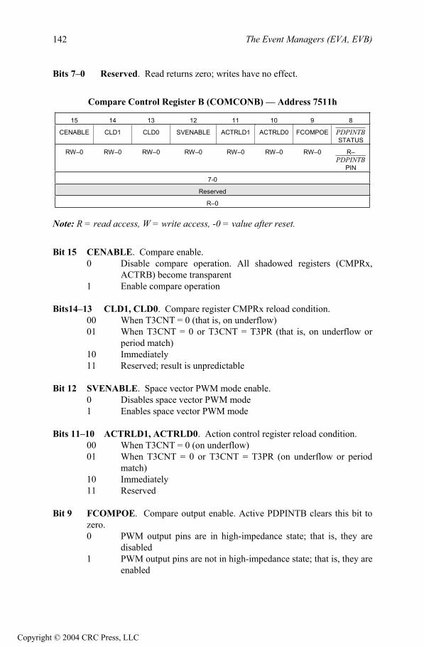
The Event Managers (EVA, EVB)142
Bits 7–0 Reserved. Read returns zero; writes have no effect.
Compare Control Register B (COMCONB) — Address 7511h
15 14 13 12 11 10 9 8
CENABLE CLD1 CLD0 SVENABLE ACTRLD1 ACTRLD0 FCOMPOE PDPINTBSTATUS
RW–0 RW–0 RW–0 RW–0 RW–0 RW–0 RW–0 R–PDPINTB
PIN
7-0
Reserved
R–0
Note: R = read access, W = write access, -0 = value after reset.
Bit 15 CENABLE. Compare enable.0 Disable compare operation. All shadowed registers (CMPRx,
ACTRB) become transparent1 Enable compare operation
Bits14–13 CLD1, CLD0. Compare register CMPRx reload condition.00 When T3CNT = 0 (that is, on underflow)01 When T3CNT = 0 or T3CNT = T3PR (that is, on underflow or
period match)10 Immediately11 Reserved; result is unpredictable
Bit 12 SVENABLE. Space vector PWM mode enable.0 Disables space vector PWM mode1 Enables space vector PWM mode
Bits 11–10 ACTRLD1, ACTRLD0. Action control register reload condition.00 When T3CNT = 0 (on underflow)01 When T3CNT = 0 or T3CNT = T3PR (on underflow or period
match)10 Immediately11 Reserved
Bit 9 FCOMPOE. Compare output enable. Active PDPINTB clears this bit tozero.0 PWM output pins are in high-impedance state; that is, they are
disabled1 PWM output pins are not in high-impedance state; that is, they are
enabled
Copyright © 2004 CRC Press, LLC

The Event Managers (EVA, EVB) 143
Bit 8 PDPINTB STATUS. This bit reflects the current status of the PDPINTBpin. (This bit is applicable to 240xA devices only — it is reserved on 240xdevices and returns a zero when read.)
Bits 7–0 Reserved. Read returns zero; writes have no effect.
Compare Action Control Registers (ACTRA and ACTRB)
The double buffered, compare action control registers (ACTRA and ACTRB) determine what action occurs on each of the six compare output pins when acompare event occurs (if the compare operation is enabled by COMCONx[15]).The compare output pins are PWMx, where x = 1–6 for ACTRA, and x = 7–12 forACTRB. The condition on which ACTRA and ACTRB are reloaded is defined bythe bits in COMCONx.
Compare Action Control Register A (ACTRA) — Address 7413h15 14 13 12 11 10 9 8
SVRDIR D2 D1 D0 CMP6ACT1 CMP6ACT0 CMP5ACT1 CMP5ACT0
RW–0 RW–0 RW–0 RW–0 RW–0 RW–0 RW–0 RW–0
7 6 5 4 3 2 1 0
CMP4ACT1 CMP4ACT0 CMP3ACT1 CMP3ACT0 CMP2ACT1 CMP2ACT0 CMP1ACT1 CMP1ACT0
RW–0 RW–0 RW–0 RW–0 RW–0 RW–0 RW–0 RW–0
Note: R = read access, W = write access, -0 = value after reset.
Bit 15 SVRDIR. Space vector PWM rotation direction. Used only in spacevector PWM output generation.0 Positive (CCW)1 Negative (CW)
Bits 14–12 D2–D0. Basic space vector bits. Used only in space vector PWM output generation.
Bits 11–10 CMP6ACT1–0. Action on compare output pin 6, CMP6.00 Forced low01 Active low10 Active high11 Forced high
Bits 9–8 CMP5ACT1–0. Action on compare output pin 5, CMP5.00 Forced low01 Active low10 Active high11 Forced high
Copyright © 2004 CRC Press, LLC

The Event Managers (EVA, EVB)144
Bits 7–6 CMP4ACT1–0. Action on compare output pin 4, CMP4.00 Forced low01 Active low10 Active high11 Forced high
Bits 5–4 CMP3ACT1–0. Action on compare output pin 3, CMP3.00 Forced low01 Active low10 Active high
Bits 3–2 CMP2ACT1–0. Action on compare output pin 2, CMP2.00 Forced low01 Active low10 Active high11 Forced high
Bits 1–0 CMP1ACT1–0. Action on compare output pin 1, CMP1.00 Forced low01 Active low10 Active high11 Forced high
Compare Action Control Register B (ACTRB) — Address 7513h15 14 13 12 11 10 9 8
SVRDIR D2 D1 D0 CMP12ACT1 CMP12ACT0 CMP11ACT1 CMP11ACT0
RW–0 RW–0 RW–0 RW–0 RW–0 RW–0 RW–0 RW–0
7 6 5 4 3 2 1 0CMP10ACT1 CMP10ACT0 CMP9ACT1 CMP9ACT0 CMP8ACT1 CMP8ACT0 CMP7ACT1 CMP7ACT0
RW–0 RW–0 RW–0 RW–0 RW–0 RW–0 RW–0 RW–0
Note: R = read access, W = write access, -0 = value after reset.
Bit 15 SVRDIR. Space vector PWM rotation direction. Used only in spacevector PWM output generation.0 Positive (CCW)1 Negative (CW)
Bits 14–12 D2–D0. Basic space vector bits. Used only in space vector PWM output generation.
Bits 11–10 CMP12ACT1–0. Action on compare output pin 12, CMP12.00 Forced low01 Active low
Copyright © 2004 CRC Press, LLC

The Event Managers (EVA, EVB) 145
10 Active high11 Forced high
Bits 9–8 CMP11ACT1–0. Action on compare output pin 11, CMP11.00 Forced low01 Active low10 Active high11 Forced high
Bits 7–6 CMP10ACT1–0. Action on compare output pin 10, CMP10.00 Forced low01 Active low10 Active high11 Forced high
Bits 5–4 CMP9ACT1–0. Action on compare output pin 9, CMP9.00 Forced low01 Active low10 Active high11 Forced high
Bits 3–2 CMP8ACT1–0. Action on compare output pin 8, CMP8.00 Forced low01 Active low10 Active high11 Forced high
Bits 1–0 CMP7ACT1–0. Action on compare output pin 7, CMP7.00 Forced low01 Active low10 Active high11 Forced high
Dead-Band Timer Control Register A (DBTCONA) — Address 7415h
15-12 11 10 9 8
Reserved DBT3 DBT2 DBT1 DBT0
R–0 RW–0 RW–0 RW–0 RW–0
7 6 5 4 3 2 1-0
EDBT3 EDBT2 EDBT1 DBTPS2 DBTPS1 DBTPS0 Reserved
RW–0 RW–0 RW–0 RW–0 RW–0 RW–0 R–0
Note: R = read access, W = write access, -0 = value after reset.
Bits 15–12 Reserved. Reads return zero; writes have no effect.
Copyright © 2004 CRC Press, LLC

The Event Managers (EVA, EVB)146
Bits 11–8 DBT3 (MSB)–DBT0 (LSB). Dead-band timer period. These bits definethe period value of the three 4-bit dead-band timers.
Bit 7 EDBT3. Dead-band timer 3 enable (for pins PWM5 and PWM6 ofCompare Unit 3). 0 Disable1 Enable
Bit 6 EDBT2. Dead-band timer 2 enable (for pins PWM3 and PWM4 ofCompare Unit 2). 0 Disable1 Enable
Bit 5 EDBT1. Dead-band timer 1 enable (for pins PWM1 and PWM2 ofCompare Unit 1). 0 Disable1 Enable
Bits 4–2 DBTPS2 to DBTPS0. Dead-band timer prescaler.000 x/1001 x/2010 x/4011 x/8100 x/16101 x/32110 x/32111 x/32x = Device (CPU) clock frequency
Bits 1–0 Reserved. Reads return zero; writes have no effect.
Dead-Band Timer Control Register B (DBTCONB) — Address 7515h
15-12 11 10 9 8
Reserved DBT3 DBT2 DBT1 DBT0
R–0 RW–0 RW–0 RW–0 RW–0
7 6 5 4 3 2 1-0
EDBT3 EDBT2 EDBT1 DBTPS2 DBTPS1 DBTPS0 Reserved
RW–0 RW–0 RW–0 RW–0 RW–0 RW–0 R–0
Note: R = read access, W = write access, -0 = value after reset.
Bits 15–12 Reserved. Reads return zero; writes have no effect.
Bits 11–8 DBT3 (MSB)–DBT0 (LSB). Dead-band timer period. These bitsdefine the period value of the three 4-bit dead-band timers.
Copyright © 2004 CRC Press, LLC

The Event Managers (EVA, EVB) 147
Bit 7 EDBT3. Dead-band timer 3 enable (for pins PWM11 and PWM12 ofCompare 6). 0 Disable1 Enable
Bit 6 EDBT2. Dead-band timer 2 enable (for pins PWM9 and PWM10 ofCompare 5). 0 Disable1 Enable
Bit 5 EDBT1. Dead-band timer 1 enable (for pins PWM7 and PWM8 ofCompare 4). 0 Disable1 Enable
Bits 4–2 DBTPS2 to DBTPS0. Dead-band timer prescaler.000 x/1001 x/2010 x/4011 x/8100 x/16101 x/32110 x/32111 x/32x = Device (CPU) clock frequency
Bits 1–0 Reserved. Reads return zero; writes have no effect.
6.5 Capture Units and Quadrature Encoded Pulse (QEP) Circuitry
The Capture Units on the LF2407 allow an event (rising/falling edge) on thecapture pin to be time stamped by a selected GP Timer. There are three Capture Units in each EV, each with its own capture input pin (CAPx). Capture Units 1, 2,and 3 are associated with EVA while Capture Units 4, 5, and 6 are associated with EVB. Each EV module contains the following (shown in Figs. 6.14 and 6.15):
One 16 bit capture control register per EV (CAPCOMA for EVA,CAPCOMB for EVB) is used for configuring the Capture Unitfunctionality.Three 16-bit, 2-level-deep First-In-First-Out (FIFO) stacks per EV(CAPxFIFO); one FIFO stack for each Capture Unit; the “captured” timer count value is stored here.One 16-bit capture status register (CAPFIFOA for EVA, CAPFIFOB forEVB); provides information on the number of timer captures in each capture FIFO.
Copyright © 2004 CRC Press, LLC

The Event Managers (EVA, EVB)148
Inputs of either GP Timer 1 or 2 (for EVA) and GP Timer 3 or 4 (for EVB)as the time base. One capture pin per Capture Unit with user-specified transition detection(rising edge, falling edge, or both edges). CAP1 through CAP3 for EVA,and CAP4 through CAP6 for EVB.Six maskable interrupt flags, one for each Capture Unit.
T2CNT GPtimer 2 counter
T1CNT GPtimer 1counter
MUX
Edgedetect
2–levelFIFO
stacks
Cap FIFOstatus
ADC start
CAPCONA[15]
CAP1,2,3
CAPCONA[8]
2
16
16
8
6
6
3
CAPCONA[9,10] CAPCONA[12-14]
RS
clear
CAPCONA[2-7]
Edgeselect
Capture unit 3cap. event
CAPFIFOA[13-15]
RS
EN
Figure 6.15 EVA capture unit diagram. (Courtesy of Texas Instruments)
Copyright © 2004 CRC Press, LLC

The Event Managers (EVA, EVB) 149
T2CNT GPtimer 4 counter
T1CNT GPtimer 3 counter
MUX
Edgedetect
2–levelFIFO
stacks
Cap FIFOstatus
ADC start
CAPCONB[15]
CAP4,5,6
CAPCONB[8]
2
16
16
8
6
6
3
CAPCONB[9,10] CAPCONB[12-14]
RS
clear
CAPCONB[2-7]
Edgeselect
Capture unit 6cap. event
CAPFIFOB[13-15]
RS
EN
Figure 6.16 EVB Capture unit diagram. (Courtesy of Texas Instruments)
The Capture Units are useful in applications where the time of an externaltrigger needs to be “captured”. For example, if we want to measure the timebetween the rising edges of two pulses, we would configure the appropriateregisters for capture operation on a specific capture pin. At each rising edge, theCapture Unit would then store the corresponding timer values. The user program could then subtract the second capture value from the first value and determine thetime between the pulses.
The Capture Units are accompanied by the Quadrature Encoded Pulse (QEP)circuitry which uses the GP Timers to “decode” a QEP signal. When the QEP modeis selected, pins CAP1 and CAP2 (CAP4 and CAP5 in case of EVB) are used asQEP inputs. More on the QEP circuitry will be discussed shortly.
Copyright © 2004 CRC Press, LLC

The Event Managers (EVA, EVB)150
6.5.1 Operation of the Capture Unit
When a Capture Unit is enabled, when either a rising or falling edge is detectedon the capture input pin (CAPx), the current value of the selected GP Timer counter is copied and stored in the corresponding capture FIFO. In order for a transition tobe captured, the input must hold at its current level for the duration of at least twoCPU clock cycles. After the GP Timer value is recorded in the capture FIFO, aninterrupt could also be generated, and software may then read the FIFO value. Thevalue from the capture FIFO can then be used in an algorithm.
While we can think of the capture FIFO as being a two-level deep singleregister, each capture FIFO stack actually consists of two registers, CAPxFIFO and CAPxBOT (for EVA x=1,2,3; EVB x=4,5,6). When a new value is stored in theFIFO during a capture, in reality it first goes to the bottom register. When the topregister of the FIFO stack is empty (either because this is the first capture, or the FIFO was just read), the value in the bottom register is automatically shifted into thetop register (CAPxFIFO). Because of the above operation, when reading from the FIFO, the FIFO will always return the oldest stored value first. When the FIFO contains two values and is read, the oldest value will be read and removed from theFIFO. On the next read, the next oldest value will be read and removed from theFIFO. Usually, only read from the CAPxFIFO register, but the bottom register ofthe stack (CAPxBOT) can also be read.
When no FIFO reads have been performed, after two captures thecorresponding capture FIFO will have two timer values stored in it and will be full.In the case that the FIFO has still not been read from and a third capture is recorded,the first capture value will be pushed out of the FIFO and lost.
The bits in the FIFO status registers indicate how many values are currentlystored in each FIFO. When a value is read from the CAPxFIFO (or bottom register,CAPxBOT), the status bits will indicate one less value in the FIFO. The two statusbits corresponding to a particular FIFO should normally indicate “00”, “01”, and“10”. If a third capture occurs and the previous two values have not been read fromthe FIFO, the status bits will indicate “11”, indicating that the oldest value was lost.In this case, after the next FIFO read, the status bits return to their usual values of “00”, “01” or “10”.
The following steps should be taken to configure the Capture Units foroperation:
1. Initialize the CAPFIFOx and clear the appropriate status bits.2. Set the selected GP Timer in the desired counting mode.3. Set the associated GP Timer compare register or GP Timer period register,
if necessary.4. Set up CAPCONA or CAPCONB as appropriate for desired operation.
Copyright © 2004 CRC Press, LLC

The Event Managers (EVA, EVB) 151
6.5.2 Capture Stack Interrupt Flag Operation:
Because the FIFO stack is two levels deep, the corresponding interrupt flag isset as soon as there are two values in the stack (the FIFO is full). This means that ifthere is one (or two) previous values in the FIFO (indicated by CAPxFIFO bits notequal to zero) and another capture takes place, the interrupt flag will be set. Like all interrupts, if the flag is unmasked, then an interrupt is generated. If interruptoperation is not desired, either the interrupt flag or the status bits can be polledcontinuously to determine if capture events have occurred.
6.5.3 Quadrature Encoded Pulse (QEP) Circuitry
QEPs are two sequences of pulses which have a variable frequency and are 90ºout of phase with one another (see Fig. 6.17). QEP signals are usually generated bya position/speed sensing device such as a rotary optical encoder. When the encoderis rotated, the direction of rotation can be determined by which sequence of pulsesleads the other. Rotational speed and position can be determined from the countand frequency of the pulses.
Figure 6.17 A pair of quadrature encoded pulses.
Each EV module has a QEP circuit associated with the Capture Units (see Figs. 6.18 and 6.19). The QEP circuit, when enabled, decodes and counts the quadratureencoded input pulses on the QEP input pins. The input pins consist of CAP1/QEP1and CAP2/QEP2 for EVA or CAP4/QEP3 and CAP5/QEP4 for EVB. When theQEP function is enabled, the compare function of the pins is disabled and the pinsare configured for QEP input.
2
CAPCONA[13,14]
2 2
2QEPdecoder
logic
GPT2 clock
GPT2 dir
T2CON[4,5]
TDIRA CLK
DIRCAP1/QEP1CAP2/QEP2
GP timer 2 Prescaler
T2CON[8,9,10]
CLKOUTCLKIN
MUX
2
Captureunit 1,2
MUX
MUX
2
Figure 6.18 QEP circuit block for EVA. (Courtesy of Texas Instruments)
Copyright © 2004 CRC Press, LLC

The Event Managers (EVA, EVB)152
2
CAPCONB[13,14]
2 2
2QEPdecoder
logic
GPT4 clock
GPT4 dir
T4CON[4,5]
TDIRBCLK
DIRCAP4/QEP3CAP5/QEP4
GP timer 4 Prescaler
T4CON[8,9,10]
CLKOUTCLKIN
MUX
2
Captureunit 4,5
MUX
MUX
2
Figure 6.19 QEP circuit for EVB. (Courtesy of Texas Instruments)
QEP Circuit Operation
The counter for the QEP circuit is provided by GP Timer 2 for EVA and GPTimer 4 for EVB. The GP Timer must be configured for directional-up/down countmode. When the QEP circuit is selected as the clock source, the timer ignores thedirection and clock (TDIRA/B and TCLKINA/B) input pins. The QEP circuit willact as the clock reference and the direction input for the timer. The QEP circuitdetermines which one of the sequences is the leading sequence. It then generates adirection signal as the direction input to the GP Timer. The timer counts up ifCAP1/QEP1 (CAP4/QEP3 for EVB) input is the leading sequence, and countsdown if CAP2/QEP2 (CAP5/QEP4 for EVB) is the leading sequence. Both edges of the pulses of the two quadrature encoded inputs are counted by the QEP circuit.Therefore, the frequency of the clock generated by the QEP logic to GP Timer 2 (or4) is four times that of each input sequence. This quadrature clock is connected to the clock input of GP Timer 2 (or 4).
Note: Upon a DSP RESET, the QEP logic will miss the first QEP edge.
Configuring for QEP Operation:
EVA:
1. Load GP Timer 2’s counter, period, and compare registers if desired; forsimple QEP decoding, this is not required.
2. Configure T2CON to set GP Timer 2 in directional-up/down mode withthe QEP circuits as clock source, and enable the selected timer.
3. Configure CAPCONA to enable the QEP circuit.
Copyright © 2004 CRC Press, LLC
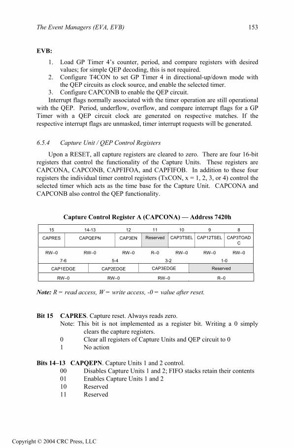
The Event Managers (EVA, EVB) 153
EVB:
1. Load GP Timer 4’s counter, period, and compare registers with desiredvalues; for simple QEP decoding, this is not required.
2. Configure T4CON to set GP Timer 4 in directional-up/down mode withthe QEP circuits as clock source, and enable the selected timer.
3. Configure CAPCONB to enable the QEP circuit.Interrupt flags normally associated with the timer operation are still operational
with the QEP. Period, underflow, overflow, and compare interrupt flags for a GPTimer with a QEP circuit clock are generated on respective matches. If therespective interrupt flags are unmasked, timer interrupt requests will be generated.
6.5.4 Capture Unit / QEP Control Registers
Upon a RESET, all capture registers are cleared to zero. There are four 16-bit registers that control the functionality of the Capture Units. These registers are CAPCONA, CAPCONB, CAPFIFOA, and CAPFIFOB. In addition to these four registers the individual timer control registers (TxCON, x = 1, 2, 3, or 4) control theselected timer which acts as the time base for the Capture Unit. CAPCONA andCAPCONB also control the QEP functionality.
Capture Control Register A (CAPCONA) — Address 7420h
15 14-13 12 11 10 9 8
CAPRES CAPQEPN CAP3EN Reserved CAP3TSEL CAP12TSEL CAP3TOADC
RW–0 RW–0 RW–0 R–0 RW–0 RW–0 RW–0
7-6 5-4 3-2 1-0
CAP1EDGE CAP2EDGE CAP3EDGE Reserved
RW–0 RW–0 RW–0 R–0
Note: R = read access, W = write access, -0 = value after reset.
Bit 15 CAPRES. Capture reset. Always reads zero. Note: This bit is not implemented as a register bit. Writing a 0 simply
clears the capture registers.0 Clear all registers of Capture Units and QEP circuit to 01 No action
Bits 14–13 CAPQEPN. Capture Units 1 and 2 control.00 Disables Capture Units 1 and 2; FIFO stacks retain their contents01 Enables Capture Units 1 and 210 Reserved11 Reserved
Copyright © 2004 CRC Press, LLC

The Event Managers (EVA, EVB)154
Bit 12 CAP3EN. Capture Unit 3 control.0 Disables Capture Unit 3; FIFO stack of Capture Unit 3 retains its
contents1 Enable Capture Unit 3
Bit 11 Reserved. Reads return zero; writes have no effect.
Bit 10 CAP3TSEL. GP Timer selection for Capture Unit 3.0 Selects GP Timer 2 1 Selects GP Timer 1
Bit 9 CAP12TSEL. GP Timer selection for Capture Units 1 and 2.0 Selects GP Timer 2 1 Selects GP Timer 1
Bit 8 CAP3TOADC. Capture Unit 3 event starts ADC. 0 No action1 Starts ADC when the CAP3INT flag is set
Bits 7–6 CAP1EDGE. Edge detection control for Capture Unit 1.00 No detection01 Detects rising edge10 Detects falling edge11 Detects both edges
Bits 5–4 CAP2EDGE. Edge detection control for Capture Unit 2.00 No detection01 Detects rising edge10 Detects falling edge11 Detects both edges
Bits 3–2 CAP3EDGE. Edge detection control for Capture Unit 3.00 No detection01 Detects rising edge10 Detects falling edge11 Detects both edges
Bits 1–0 Reserved. Reads return zero; writes have no effect.
Copyright © 2004 CRC Press, LLC

The Event Managers (EVA, EVB) 155
Capture Control Register B (CAPCONB) — Address 7520h
15 14-13 12 11 10 9 8
CAPRES CAPQEPN CAP6EN Reserved CAP6TSEL CAP45TSEL CAP6TOADC
RW–0 RW–0 RW–0 R–0 RW–0 RW–0 RW–0
7-6 5-4 3-2 1-0
CAP4EDGE CAP5EDGE CAP6EDGE Reserved
RW–0 RW–0 RW–0 RW–0
Note: R = read access, W = write access, -0 = value after reset.
Bit 15 CAPRES. Capture reset. Always reads zero. Note: This bit is not implemented as a register bit. Writing a 0 simply
clears the capture registers.0 Clears all registers of Capture Units and QEP circuit to 01 No action
Bits 14–13 CAPQEPN. Capture Units 4 and 5 and QEP circuit control.00 Disables Capture Units 4 and 5 and QEP circuit. FIFO stacks
retain their contents01 Enables Capture Units 4 and 5, disable QEP circuit10 Reserved11 Enables QEP circuit. Disable Capture Units 4 and 5; bits 4–7 and
9 are ignored
Bit 12 CAP6EN. Capture Unit 6 control.0 Disables Capture Unit 6; FIFO stack of Capture Unit 6 retains its
contents1 Enables Capture Unit 6
Bit 11 Reserved. Reads return zero; writes have no effect.
Bit 10 CAP6TSEL. GP Timer selection for Capture Unit 6.0 Selects GP Timer 4 1 Selects GP Timer 3
Bit 9 CAP45TSEL. GP Timer selection for Capture Units 4 and 5.0 Selects GP Timer 4 1 Selects GP Timer 3
Bit 8 CAP6TOADC. Capture Unit 6 event starts ADC. 0 No action1 Starts ADC when the CAP6INT flag is set
Copyright © 2004 CRC Press, LLC

The Event Managers (EVA, EVB)156
Bits 7–6 CAP4EDGE. Edge detection control for Capture Unit 4.00 No detection01 Detects rising edge10 Detects falling edge11 Detects both edges
Bits 5–4 CAP5EDGE. Edge detection control for Capture Unit 5.00 No detection01 Detects rising edge10 Detects falling edge11 Detects both edges
Bits 3–2 CAP6EDGE. Edge detection control for Capture Unit 6.00 No detection01 Detects rising edge10 Detects falling edge11 Detects both edges
Bits 1–0 Reserved. Reads return zero; writes have no effect.
Capture Status Registers
The ability to write to the CAPFIFOx registers can be used as a programmingadvantage. For example, if a “01” is written to the CAPnFIFO bits by user code, theEV module is led to believe that there is already an entry in the FIFO. Subsequently,every time the FIFO gets a new value, a capture interrupt will be generated. If awrite occurs to the CAPnFIFOA status bits at the same time as they are beingupdated by hardware (because of a capture event), the user written data takesprecedence.
Capture FIFO Status Register A (CAPFIFOA) — Address 7422h
15-14 13-12 11-10 9-8
Reserved CAP3FIFO CAP2FIFO CAP1FIFO
R–0 RW –0 RW –0 RW –0
7-0
Reserved
R–0
Note: R = read access, W = write access, -0 = value after reset.
Bits 15–14 Reserved. Reads return zero; writes have no effect.
Bits 13–12 CAP3FIFO. CAP3FIFO Status 00 Empty01 Has one entry10 Has two entries
Copyright © 2004 CRC Press, LLC

The Event Managers (EVA, EVB) 157
11 Had two entries and captured another one; first entry has been lost
Bits 11–10 CAP2FIFO. CAP2FIFO Status 00 Empty01 Has one entry10 Has two entries11 Had two entries and captured another one; first entry has been lost
Bits 9–8 CAP1FIFO. CAP1FIFO Status00 Empty01 Has one entry10 Has two entries11 Had two entries and captured another one; first entry has been lost
Bits 7–0 Reserved. Reads return zero; writes have no effect.
Capture FIFO Status Register B (CAPFIFOB) — Address 7522h
15-14 13-12 11-10 9-8
Reserved CAP6FIFO CAP5FIFO CAP4FIFO
R–0 RW –0 RW –0 RW –0
7-0
Reserved
R–0
Note: R = read access, W = write access, -0 = value after reset.
Bits 15–14 Reserved. Reads return zero; writes have no effect.
Bits 13–12 CAP6FIFO. CAP6FIFO Status 00 Empty01 Has one entry10 Has two entries11 Had two entries and captured another one; first entry has been lost
Bits 11–10 CAP5FIFO. CAP5FIFO Status 00 Empty01 Has one entry10 Has two entries11 Had two entries and captured another one; first entry has been lost
Bits 9–8 CAP4FIFO. CAP4FIFO Status00 Empty01 Has one entry10 Has two entries11 Had two entries and captured another one; first entry has been lost
Copyright © 2004 CRC Press, LLC

The Event Managers (EVA, EVB)158
Bits 7–0 Reserved. Reads return zero; writes have no effect.
6.6 General Event Manager Information
Table 6.5 Event Manager A (EVA) Pins
Pin Name DescriptionCAP1/QEP1 Capture Unit 1 input, QEP circuit input 1CAP2/QEP2 Capture Unit 2 input, QEP circuit input 2CAP3 Capture Unit 3 inputPWM1 Compare Unit 1 output 1PWM2 Compare Unit 1 output 2PWM3 Compare Unit 2 output 1PWM4 Compare Unit 2 output 2PWM5 Compare Unit 3 output 1PWM6 Compare Unit 3 output 2T1CMP/T1PWM Timer 1 compare/PWM outputT2CMP/T2PWM Timer 2 compare/PWM outputTCLKINA External clock-in for timers in EVA ( when
configured to operate from external clock)TDIRA External timer direction input in EVA ( when timer is
in directional up/down mode)
Table 6.6 Event Manager B (EVB) Pins
Pin Name DescriptionCAP4/QEP3 Capture Unit 4 input, QEP circuit input 3CAP5/QEP4 Capture Unit 5 input, QEP circuit input 4CAP6 Capture Unit 6 inputPWM7 Compare Unit 4 output 1PWM8 Compare Unit 4 output 2PWM9 Compare Unit 5 output 1PWM10 Compare Unit 5 output 2PWM11 Compare Unit 6 output 1PWM12 Compare Unit 6 output 2T3CMP/T3PWM Timer 3 compare/PWM outputT4CMP/T4PWM Timer 4 compare/PWM outputTCLKINB External clock-in for timers in EVB (when
configured to operate from external clock)TDIRB External timer direction input in EVB (when timer is
in directional up/down mode)
NOTE: Most of the EV pins are mapped with a second function. In order to use theEV, you must configure the appropriate pins to their EV function. For moreinformation on how pin sharing works and how to configure pins refer to Chapter 4.
Copyright © 2004 CRC Press, LLC

The Event Managers (EVA, EVB) 159
Event Manager (EV) Register Addresses
Table 6.7 Addresses of EVA Timer Registers
Address Register Name7400h GPTCONA GP Timer control register A7401h T1CNT Timer 1 counter register Timer 1 7402h T1CMPR Timer 1 compare register
7403h T1PR Timer 1 period register7404h T1CON Timer 1 control register7405h T2CNT Timer 2 counter register7406h T2CMPR Timer 2 compare register Timer 2 7407h T2PR Timer 2 period register7408h T2CON Timer 2 control register
Table 6.8 Addresses of EVB Timer Registers
Address Register Name7500h GPTCONB GP Timer control register B7501h T3CNT Timer 3 counter register7502h T3CMPR Timer 3 compare register Timer 3 7503h T3PR Timer 3 period register7504h T3CON Timer 3 control register
7505h T4CNT Timer 4 counter register7506h T4CMPR Timer 4 compare register Timer 4 7507h T4PR Timer 4 period register7508h T4CON Timer 4 control register
Table 6.9 Addresses of EVA Compare Control Registers
Address Register Name7411h COMCONA Compare control register7413h ACTRA Compare action control register7415h DBTCONA Dead-band timer control register7417h CMPR1 Compare register 17418h CMPR2 Compare register 27419h CMPR3 Compare register 3
Copyright © 2004 CRC Press, LLC

The Event Managers (EVA, EVB)160
Table 6.10 Addresses of EVB Compare Control Registers
Address Register Name7511h COMCONB Compare control register7513h ACTRB Compare action control register7515h DBTCONB Dead-band timer control register7517h CMPR4 Compare register 47518h CMPR5 Compare register 57519h CMPR6 Compare register 6
Table 6.11 Addresses of EVA Capture Registers
Address Register Name7420h CAPCONA Capture control register7422h CAPFIFOA Capture FIFO status register7423h CAP1FIFO Two-level-deep capture FIFO stack 17424h CAP2FIFO Two-level-deep capture FIFO stack 27425h CAP3FIFO Two-level-deep capture FIFO stack 37427h CAP1FBOT Bottom registers of FIFO stacks;
allows most recent CAPTURE valueto be read
7428h CAP2FBOT
7429h CAP3FBOT
Table 6.12 Addresses of EVB Capture Registers
Address Register Name7520h CAPCONB Capture control register7522h CAPFIFOB Capture FIFO status register7523h CAP4FIFO Two-level-deep capture FIFO stack 47524h CAP5FIFO Two-level-deep capture FIFO stack 57525h CAP6FIFO Two-level-deep capture FIFO stack 67527h CAP4FBOT Bottom registers of FIFO stacks,
allows most recent CAPTURE valueto be read
7528h CAP5FBOT
7529h CAP6FBOT
Copyright © 2004 CRC Press, LLC

The Event Managers (EVA, EVB) 161
Table 6.13 Addresses of EVA Interrupt Registers
Address Register Name742Ch EVAIMRA Interrupt mask register A 742Dh EVAIMRB Interrupt mask register B742Eh EVAIMRC Interrupt mask register C742Fh EVAIFRA Interrupt flag register A 7430h EVAIFRB Interrupt flag register B7431h EVAIFRC Interrupt flag register C
Table 6.14 Addresses of EVB Interrupt Registers
Address Register Name752Ch EVBIMRA Interrupt mask register A 752Dh EVBIMRB Interrupt mask register B752Eh EVBIMRC Interrupt mask register C752Fh EVBIFRA Interrupt flag register A 7530h EVBIFRB Interrupt flag register B7531h EVBIFRC Interrupt flag register C
6.7 Exercise: PWM Signal Generation
As discussed in the previous sections, there are two ways to generate a PWMsignal on the LF2407: through the GP Timer compare operation, or the CompareUnits. This exercise will allow you to use your knowledge of the LF2407 DSP towrite code that will generate PWM signals on both the GP Timer and Compare Unitoutputs.
Procedure:
1. Write a program that outputs a fixed duty cycle “PWM” on a GP Timer 2 compare pin. Create the program so that the period of the PWM signal is 1 kHz and the duty cycle (on time/period) is fixed at 75%. The informationon the GP Timer compare operation in the previous section will be veryuseful in writing this code.
2. View the output (1 kHz fixed duty cycle signal) on theT1PWM/T1CMP/IOPB4 pin. The Spectrum Digital LF2407 EVMschematic will be helpful in determining the location of this pin connectionon the EVM.
3. If available, connect this fixed duty cycle signal to a dc voltage converterand use it to control the speed of a dc motor by varying the duty cycle of the waveform.
4. Modify the above program to now create a sinusoidally modulated PWMsignal on the GP Timer Compare pin. To do this, a sinusoidal look-up
Copyright © 2004 CRC Press, LLC

The Event Managers (EVA, EVB) 162
table can be created separately and then included with the source code. To modulate the signal, the timer compare register needs to be repeatedly updated with the modulation signal at a desired rate for a particular sinusoidal output frequency.
5. Write another program that creates the sinusoidal PWM, but instead uses the Compare Units.
6. If available, connect the two PWM outputs of the compare unit to a power inverter and run a single-phase induction motor. Vary the speed of the motor by manually varying the magnitude and rate at which the compare registers are updated with the modulation signal. Maintain a constant voltage/frequency (V/Hz) ratio to the induction motor.
Copyright © 2004 CRC Press, LLC

Chapter 7
DSP-BASED IMPLEMENTATION OF DC-DC BUCK-BOOST
CONVERTERS
7.1 Introduction
In a large number of industrial applications, it is required to convert a dcvoltage to a different dc voltage level, often with a regulated output. To performthis task, a dc-dc converter is needed. A dc-dc converter directly converts a dcvoltage of one level to another. It can be used to step-down (buck), or step-up(boost) a dc voltage source. In this chapter, the DSP-based control of a buck-boost,a specific type of dc-dc converter, is explained.
7.2 Converter Structure
The buck-boost converter has the structure shown in Fig. 7.1. The principle ofoperation is that when the transistor T is turned on, the input voltage V is appliedacross the inductor L and the current i in the inductor rises. Then the transistor is turned off. The current in the inductor must continue to flow somehow, and consequently finds its path through the load resistor R, and back to the inductorthrough the diode D. This discharges the inductor, and the current through it decreases. The capacitor filters the output voltage ripple. The description givenin the above is with the continuous conduction mode, meaning the inductor currentnever goes discontinuous. The continuous mode will be discussed further in thenext section.
inL
C
This converter has two dominant characteristics: the output voltage is always negative with respect to the input voltage and the output voltage may be higher orlower than the input voltage. This is why this converter may also be referred to as a step-up/step-down converter.
T
D
CL R
Vin
Vout
Iout
Id
VL
IL
Figure 7.1 Buck-boost converter structure.
163
Copyright © 2004 CRC Press, LLC

DSP-Based Implementation of DC-DC Buck-Boost Converters164
7.3 Continuous Conduction Mode
The input and output voltages are related by the following equation:
inout Vd
dV1
(7.1)
In this equation, d is the transistor or switch duty cycle. Figure 7.2 shows theswitching pattern command to turn on or off, which must be fed to the transistor for proper operation of the buck-boost converter.
TransistorState
ON OFF
0 d.Ts Ts
Figure 7.2 Transistor switching pattern.
Obviously, the duty cycle may vary only from 0 to 1. The resulting values forthe converter voltage gain are:
00in
outV
VGd (7.2)
in
outV
VGd 1 (7.3)
The theoretical gain range achievable is potentially very large. Practically, it islimited by the parasitic characteristics of the converter. In addition, it is oftendesirable to keep the duty cycle between 0.1 (10%) and 0.9 (90%) for practicalengineering considerations. The relationship between the converter duty cycle andits gain, shown in Fig. 7.3, is non-linear.
0 10 20 30 40 50 60 70 80 90 1000
1
2
3
4
5
6
7
8
9
10
Converter duty cycle in %
Con
verte
r vol
tage
gai
n
Figure 7.3 Converter voltage gain versus converter duty cycle.
Copyright © 2004 CRC Press, LLC

DSP-Based Implementation of DC-DC Buck-Boost Converters 165
7.4 Discontinuous Conduction Mode
The switching results in a cyclic current increase and decrease in the inductor. This current ripple has a non-negligible influence on the operation of the converter.If during the switching period T (shown in Fig. 7.2) the current never goes to zero,then the converter is said to operate in continuous conduction mode.
s
However, if the current does go to zero at any time, then the conduction is saidto be discontinuous. In discontinuous conduction mode, the voltage gain of theconverter is not solely a function of the duty cycle, but also of the output current.An example of a discontinuous conduction current waveform is shown in Fig. 7.4.
0 d.Ts T s Ts
IL
Io I
Figure 7.4 Discontinuous conduction mode current waveform.
7.5 Connecting the DSP to the Buck-Boost Converter
To fully control the buck-boost converter voltage and current with a DSP, onedigital output and two analog inputs are required from the DSP. Figure 7.5 shows a conceptual connection diagram between the DSP and converter. The DSP willoutput a PWM switching waveform to the converter. The DSP will also receiveinformation of the instantaneous current and voltage from the load via the analog to digital converter inputs. The following subsections describe the circuits necessaryfor interfacing the DSP to the dc-dc converter.
Copyright © 2004 CRC Press, LLC
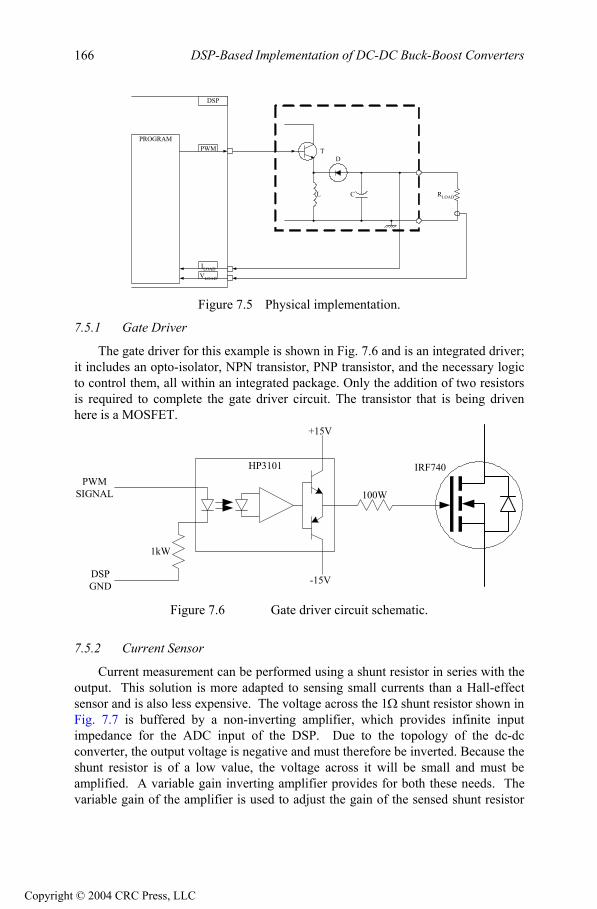
DSP-Based Implementation of DC-DC Buck-Boost Converters166
L C
DT
RLOAD
DSP
PWMPROGRAM
VLOAD
ILOAD
Figure 7.5 Physical implementation.
7.5.1 Gate Driver
The gate driver for this example is shown in Fig. 7.6 and is an integrated driver;it includes an opto-isolator, NPN transistor, PNP transistor, and the necessary logicto control them, all within an integrated package. Only the addition of two resistorsis required to complete the gate driver circuit. The transistor that is being drivenhere is a MOSFET.
+15V
-15V
100WPWM
SIGNAL
DSPGND
1kW
IRF740HP3101
Figure 7.6 Gate driver circuit schematic.
7.5.2 Current Sensor
Current measurement can be performed using a shunt resistor in series with theoutput. This solution is more adapted to sensing small currents than a Hall-effectsensor and is also less expensive. The voltage across the 1 shunt resistor shown inFig. 7.7 is buffered by a non-inverting amplifier, which provides infinite inputimpedance for the ADC input of the DSP. Due to the topology of the dc-dcconverter, the output voltage is negative and must therefore be inverted. Because the shunt resistor is of a low value, the voltage across it will be small and must beamplified. A variable gain inverting amplifier provides for both these needs. Thevariable gain of the amplifier is used to adjust the gain of the sensed shunt resistor
Copyright © 2004 CRC Press, LLC

DSP-Based Implementation of DC-DC Buck-Boost Converters 167
voltage signal. The output of the amplifier is connected to an opto-isolator, whichchanges the signal path from electrical to optical, then back to an electrical signal. The optical transmission provides the necessary galvanic insulation between thepower side of the converter and the DSP. This isolation is necessary because theDSP is a very sensitive device, while the converter is a major source of voltagesurges and interferences. The operational amplifier feeds the input, or luminescentdiode, of the opto-isolator. The output of the opto-isolator feeds into the DSP analog input. A variable collector resistor is used to set the offset voltage of theADC input.
+
-+
-
DSP +3.3V
ADCIN1
DSP GND
1k1k
1k
10k
1k
LM741LM741
TLP550 4.7k
IOUTPUT
SHUNT1W
IOUTPUT
Figure 7.7 Current sensor circuit schematic.
7.5.3 Voltage Sensor
The voltage sensor uses the same circuit as the current sensor, but with a few differences. The output voltage of the converter is directly measurable and isdirectly fed into the infinite impedance buffer. The inverting amplifier is also slightly different in that it uses a 1k resistor instead of a 10k resistor. Thedifference is that while the current signal has to be amplified, the voltage level of the converter output must be attenuated to match the acceptable voltage range of theADC input.
+
-+
-
DSP +3.3V
ADCIN0
DSP GND
VOUTPUT
1k1k
1k
1k
1k
LM741LM741
TLP550 4.7k
Figure 7.8 Voltage sensor circuit schematic.
Copyright © 2004 CRC Press, LLC
DSP-Based Implementation of DC-DC Buck-Boost Converters168
7.6 Controlling the Buck-Boost Converter
The controller of a buck-boost converter usually has two objectives:
Controlling the output voltage to a predetermined valueProtecting the converter by limiting the output current to a predeterminedvalue
Obviously, simply regulating the output voltage is the normal mode for thecontroller. If the load is such that the converter output voltage causes the current togo beyond the limit, then the controller must also control the converter to preventthe current from exceeding the maximum limit. Maintaining the current below themaximum is necessary in order to keep the converter and load from overheating.Because current regulation is necessary for safety, it must have the highest priority over all the other tasks in the control system, including the voltage regulation. Thismeans that under any variation of the load, the current will be kept below its maximum.
The proposed control scheme has the following properties:
The voltage will be regulated using a closed-loop PI regulator.
The current will be checked every switching cycle, and if its value is abovethe limit, then the voltage regulation will be suspended. This will beachieved by setting the error signal to zero, which will disable theproportional action and disable the integration of the voltage error. Theintegrator is decremented by 1 every cycle in order to smoothly bring thevoltage to a value, which will keep the current at its limit.
The current regulation is effective if the current is only slightly above thelimit. It is not effective against sudden surges such as a short circuit. If thecurrent is above two times the maximum, then the controller will reset the PWM generation (thus shutting down the transfer of power from the sourceto the load) and reset the integrator. This will cause the converter restartfrom zero voltage in voltage regulation mode. Since the voltage is verylow, the current will be slightly beyond the current limit, thus causing thecontroller to enter the current regulation mode. This is effective becauseoutput filter capacitor will be quickly discharged by a short circuit, andthus the output voltage will be zero. The voltage necessary for keeping thecurrent below the limit in a short circuit condition is very low (in the order of a few mV), so the recovery from a short circuit should happen quickly.
Regulating the output voltage can be achieved easily by means of an integralregulator in a negative feedback loop. The integral regulator outputs a command ofgain for the converter. For optimum performance, this command should belinearized; that is, converted into a useful duty cycle using the following equation:
Copyright © 2004 CRC Press, LLC

DSP-Based Implementation of DC-DC Buck-Boost Converters 169
1GainGaind (7.4)
However, this is not mandatory because the negative feedback and the integralregulator ultimately ensure the convergence of the output voltage toward thereference. In addition, the DSP is very fast in reacting to variations in the system.Equation (7.4) is theoretical and does not take into account the parasitic elements ofthe system, which make the voltage gain a different function of the duty cycle. Thetheoretical voltage gain as a function of the duty cycle and the actual gain areplotted in Fig. 9. One sees that the two curves differ slightly. A look-up table wouldbe the most accurate and simplest way to linearize the function. The voltage regulation is described using the block diagram shown in Fig. 7.10.
0 0.1 0.2 0.3 0.4 0.5 0.6 0.7 0.80
0.5
1
1.5
2
2.5
3
3.5
4
PWM duty cycle
Theo
retic
al v
olta
ge g
ain
(up)
/ A
ctua
l vol
tage
gain
(bot
tom
)
Figure 7.9 Divergence between theoretical and actual voltage gains.
+-
V_REF
V_AVERAGED
P
VOUTPUT
AVERAGING
IV_ERROR
PROBE
++
V_SAMPLE
ACTION
BUCK-BOOSTCONVERTER
Figure 7.10 Voltage regulation block diagram.
Copyright © 2004 CRC Press, LLC

DSP-Based Implementation of DC-DC Buck-Boost Converters170
This block diagram will be calculated once every switching cycle, which is themaximum speed at which parameters may be updated. Calculating the regulationmore often would be useless because the actuator, the PWM generator, would notreact until the next cycle.
The block diagram shown in Fig. 7.11 is implemented within the voltageregulation code in two sequences: current regulation and regulation reset.
READ AVERAGED CURRENT
IS CURRENT > MAXIMUM ?
IS CURRENT > 2 * MAXIMUM ?
YES
NO
NO
YES
RESET DUTY CYCLE TO ZERO
RESET INTEGRATOR
RESET V_ERROR TO ZERO
DECREMENT INTEGRATOR BY 1
TO VOLTAGEREGULATION PROGRAM
FROMVOLTAGE
REGULATION PROGRAM
Figure 7.11 Current regulation algorithm.
Figure 7.12 illustrates the flow chart of the program developed in this chapter.Notice that several loops are used in the program.
Copyright © 2004 CRC Press, LLC

DSP-Based Implementation of DC-DC Buck-Boost Converters 171
YES
START
INITIALIZEDSP
INITIALIZEVARIABLES
INITIALIZEADC
INITIALIZEPWM
GENERATION
INITIALIZESAMPLING
PERIODINTERRUPT
WAIT FORINTERRUPT
HAS ANINTERRUPTOCCURRED
?
NO
READ VOLTAGESENSOR
FORMATVOLTAGESAMPLE
READ CURRENTSENSOR
FILTER ADCMEASURES
TIME TO RUNREGULATION ?
NO
YES
AVERAGE THEMEASURES
CALCULATETHE ERROR
CURRENTREGULATION
IS CURRENT >MAXIMUM ?
YES
NO
CALCULATE PIREGULATOR
OUTPUT
IS CURRENT >2 * MAXIMUM ?
YES
RESETREGULATION
NO
OUTPUT ACTIONTO PWM
Figure 7.12 General program flow-chart.
7.7 Main Assembly Section Code Description
7.7.1 Variables Initialization
The block of code below initializes the defined variables with constants.
LDP #06h
SPLK #0900h, V_OFFSET ;Voltage probe offset * 2^6
SPLK #0880h, I_OFFSET ;Current probe offset * 2^6
SPLK #0000h, V_SAMPLE ;Voltage sample
SPLK #0000h, I_SAMPLE ;Current sample
SPLK #0000h, V_SUM ;Voltage sum
SPLK #0000h, I_SUM ;Current sum
SPLK #0000h, V_AVERAGED ;Voltage averaged
Copyright © 2004 CRC Press, LLC

DSP-Based Implementation of DC-DC Buck-Boost Converters172
SPLK #0000h, I_AVERAGED ;Current averaged
SPLK #0138h, V_REF ;Voltage reference=5V=5000d/16d
SPLK #0000h, ACTION ;Action output by the regulator
SPLK #00FAh, I_LIMIT ;Current limit FAh = 250d= 25mA
SPLK #0000h, V_ERROR ;Error of voltage regulation
SPLK #0000h, INTEGRAL ;Regulation integrator
SPLK #0000h, INT_CNT ;Interrupt counter
7.7.2 Initialization of the ADC
This code initializes the Analog-to-Digital Converter hardware of the LF2407 thatperforms the analog current and voltage sensing.
LDP #ADCTRL1>>7h ;Set data page corresponding to
;ADCcontrol registers
SPLK #0100000000000000b, ADCTRL1
;Reset ADC
SPLK #0011000000000000b, ADCTRL1
;Set ADC for Bit 6=0 start-stop
;mode
SPLK #0001h, MAXCONV ;Set for 2 conversions (2
;channels)
SPLK #0010h, CHSELSEQ1 ;Set for conversion on channel 1
;and 0
SPLK #0100000000000000b, ADCTRL2
;Reset sequencer
SPLK #0000000100000000b, ADCTRL2
;Enables ADC to be started by an
;event(timer 2 period here)
7.7.3 Initialization of GP Timer 1 for PWM Generation
This code sets the parameters of the PWM waveform generation. The period is set for a 1kHz carrier frequency. The duty cycle is set to a near zero value.
LDP #0E1h ;Set data page corresponding to
;GPIO pin registers
SPLK #0FFFFh, MCRA ;Set GPIO pins for primary
;function (IO)
LDP #GPTCONA>>7h ;Set data page corresponding to
;general purpose timer control
;register
SPLK #00000h, T1CNT ;Reset timer 1 counter
SPLK #3FFFh, T1PR ;Set timer 1 period to ~= 1ms
SPLK #3FF0h, T1CMPR ;Set duty cycle
Copyright © 2004 CRC Press, LLC
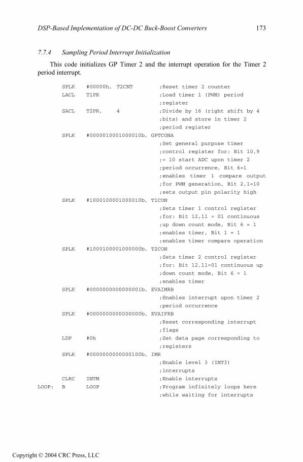
DSP-Based Implementation of DC-DC Buck-Boost Converters 173
7.7.4 Sampling Period Interrupt Initialization
This code initializes GP Timer 2 and the interrupt operation for the Timer 2 period interrupt.
SPLK #00000h, T2CNT ;Reset timer 2 counter
LACL T1PR ;Load timer 1 (PWM) period
;register
SACL T2PR, 4 ;Divide by 16 (right shift by 4
;bits) and store in timer 2
;period register
SPLK #0000010001000010b, GPTCONA
;Set general purpose timer
;control register for: Bit 10,9
;= 10 start ADC upon timer 2
;period occurrence, Bit 6=1
;enables timer 1 compare output
;for PWM generation, Bit 2,1=10
;sets output pin polarity high
SPLK #1000100001000010b, T1CON
;Sets timer 1 control register
;for: Bit 12,11 = 01 continuous
;up down count mode, Bit 6 = 1
;enables timer, Bit 1 = 1
;enables timer compare operation
SPLK #1000100001000000b, T2CON
;Sets timer 2 control register
;for: Bit 12,11=01 continuous up
;down count mode, Bit 6 = 1
;enables timer
SPLK #0000000000000001b, EVAIMRB
;Enables interrupt upon timer 2
;period occurrence
SPLK #0000000000000000b, EVAIFRB
;Reset corresponding interrupt
;flags
LDP #0h ;Set data page corresponding to
;registers
SPLK #0000000000000100b, IMR
;Enable level 3 (INT3)
;interrupts
CLRC INTM ;Enable interrupts
LOOP: B LOOP ;Program infinitely loops here
;while waiting for interrupts
Copyright © 2004 CRC Press, LLC

DSP-Based Implementation of DC-DC Buck-Boost Converters174
7.8 Interrupt Service Routine
Once an interrupt has occurred, the algorithm will perform several tasks asshown in Fig. 7.12. After the sensor voltage and current values are obtained, thealgorithm either returns to the main wait loop or branches to the regulation code.
The code sequence below is in charge of identifying what event caused theinterrupt. Reading the PIVR register obtains contains the identification number ofthe occurring interrupt. If the PIVR number corresponds to the Timer 2 periodmatch interrupt (#002Bh), then the DSP branches to the regulation code. Otherwise,it branches back to the wait loop (LOOP:) in the main code.
PERIOD:LDP #PIVR>>7h ;Set data page corresponding to
;PIVR register
LACL PIVR ;Load content of PIVR register
;to accumulator
SUB #002Bh ;Subtract number of timer 2
;period match interrupt
BCND REGULATION, EQ ;If content matches, then branch
;to regulation code
CLRC INTM ;Otherwise clear interrupt mask
;to re-enable interrupts
RET ;And return to wait loop in main
;code
7.8.1 Reading Voltage Sensors
This section of code contains protection against negative values that may occurbecause of physical sensor drift. A negative value must be eliminated. The probeoffset is determined manually when physically connecting the DSP to the converter.The block of code below reads in the voltage from the ADC result register.
LDP #RESULT0>>7h ;Set data page corresponding to
;ADC registers
LACL RESULT0 ;Load result register 1 content
;(i.e. current sample) to
;accumulator
LDP #06h ;Set data page corresponding to
;variables
SUB V_OFFSET ;Subtract voltage probe offset
BCND S1, GEQ ;If the result is positive or
;zero, then branch to proceed
;normally
LACL #0000h ;Otherwise, set result to zero
S1: SACL V_SAMPLE, 10 ;Right shift result by 10 bits
;and store it. The 6-bit shift
Copyright © 2004 CRC Press, LLC

DSP-Based Implementation of DC-DC Buck-Boost Converters 175
;is because the 6 LSBs of the
;result register are
;insignificant. The 4-bit shift
;is for formatting purposes.
7.8.2 Formatting the Voltage Sample
The voltage sample read from the A/D converter needs to be multiplied by thevalue 14d (=Eh) in order to change the value into the 16mV per digit format.
LDP #06h ;Set data page corresponding to
;variables
LT V_SAMPLE ;Load voltage sample to
;multiplier
MPY #00Eh ;Multiply by 14d
SPL V_SAMPLE ;Store 16 least significant bits
;of the result to V_SAMPLE
7.8.3 Reading the Current Sensors
This code is similar to the code that reads the voltage sensors, with theexception of the channel read, which is channel 1 here instead of channel 0. Aswith the voltage reading code, the code below reads the result register of the ADCthat contains the result from the current measurement.
LDP #RESULT1>>7h ;Set data page corresponding to
;ADC registers
LACL RESULT1 ;Load result register 1 content
;(i.e. current sample) to
;accumulator
LDP #06h ;Set data page corresponding to
;variables
SUB I_OFFSET ;Subtract current probe offset
BCND S2, GEQ ;If result is positive or zero
;then branch to proceed normally
LACL #0000h ;Otherwise, set result to zero
S2: SACL I_SAMPLE, 6 ;Right shift result by 6 bits
;and store it. Right shift is
;because the 6 LSBs are
;insignificant
7.8.4 Filtering the ADC Readings
This code accumulates the voltage and current samples from every interrupt in order to calculate their averages once every PWM cycle.
LDP #06h ;Set data page corresponding to
Copyright © 2004 CRC Press, LLC

DSP-Based Implementation of DC-DC Buck-Boost Converters176
;variables
LACL V_SUM ;Load voltage sample sum to
;accumulator
ADD V_SAMPLE ;Add voltage sample to
;accumulator
SACL V_SUM ;Store result as voltage sum
LACL I_SUM ;Load current sample sum to
;accumulator
ADD I_SAMPLE ;Add current sample to
;accumulator
SACL I_SUM ;Store result as current sum
7.9 The Regulation Code Sequences
The following sequences described in this section execute once every Timer 2 period interrupt. The Timer 2 period interrupt is set to occur at a frequency of 16times that of the PWM switching frequency. This ensures that the regulation is calculated only once every PWM cycle.
The code checks the counter of interrupt occurrence (INT_CNT). Every timethe four least significant bits are equal to 15 (every 16 interruptions), the DSP branches to the regulation code. Otherwise, it returns directly from the interruptservice routine.
LDP #06h ;Set data page corresponding to
;variables
LACL INT_CNT ;Load interrupt occurrence
;counter into accumulator
ADD #1h ;Increment by 1
SACL INT_CNT ;Store back as interrupt
;occurrence counter
AND #000Fh ;Discard all bits but 4 LSBs
XOR #000Fh ;Check for equality with 16d=Fh
BCND S_RET, NEQ ;If not, then branch to return
;from interrupt
7.9.1 Calculating the Voltage and Current Average Values
This sequence takes the sum of 16 voltage and current samples and divides itby 16. The division is performed with a 4-bit right shift. The results are theaveraged values of the load voltage and current.
LDP #06h ;Set data page corresponding to
;variables
LACL V_SUM ;Load sum of voltage sample to
;accumulator
SACL V_AVERAGED, 4 ;Shift right by 4 bits and store
Copyright © 2004 CRC Press, LLC

DSP-Based Implementation of DC-DC Buck-Boost Converters 177
;as the average load voltage
SPLK #0000h, V_SUM ;Reset sum of voltage samples
LACL I_SUM ;Load sum of current samples to
;accumulator
SACL I_AVERAGED, 4 ;Shift right by 4 bits and store
;as the average load current
SPLK #0000h, I_SUM ;Reset sum of current samples
7.9.2 Voltage Comparator
This code simply outputs the difference between the voltage reference(V_REF) and the averaged load voltage (V_AVERAGED) as the error(V_ERROR).
LDP #06h ;Set data page corresponding to
;variables
ACL V_REF ;Load voltage reference in the
;accumulator
SUB V_AVERAGED ;Subtract the averaged load
;voltage. The accumulator now
;contains the difference
SACL V_ERROR ;Store the result as V_ERROR
7.9.3 Current Regulation
This sequence checks the averaged load current versus the predefined limit and,if necessary, stops the integration of the voltage error and decrements the integrator.
LDP #06h ;Set data page corresponding to
;variables
LACL I_LIMIT ;Load maximum current value to
;accumulator
SUB I_AVERAGED ;Subtract actual averaged
;current value
BCND S3, GEQ ;If actual current below maximum
;then branch to proceed normally
SPLK #0000h, V_ERROR ;Otherwise, stop integrating
;voltage error
LACL INTEGRAL :And load integral value
SUB #1h ;Decrement it by 1
SACL INTEGRAL ;Store it back as integral value
7.9.4 PI Regulator
The code below is actually only an integral regulator, which proved to be sufficient for the application.
Copyright © 2004 CRC Press, LLC

DSP-Based Implementation of DC-DC Buck-Boost Converters178
S3: LDP #06h ;Set data page corresponding to
;variables
LACL INTEGRAL ;Load integral value to
;accumulator
ADD V_ERROR ;Integrate the error
SACL INTEGRAL ;Store result as integral value
SACL ACTION, 3 ;Right shift by 3 bits for
;formatting purposes and output
;result as action
7.9.5 Short Circuit Protection
The protection algorithm is activated if the average current rises to twice thelimit. This sequence executes along with the rest of the regulation code. Theprotection algorithm must immediately reset the PWM output and the integrator tozero in order to protect the buck-boost converter and load against sudden surges of current. It should be noted that in case of a short-circuit, this protection will beactivated only a few times. Once the filter capacitor is discharged, the load currentwill drop to acceptable levels and the LF2407 will work in current regulation mode.
LDP #06h ;Set data page corresponding to
;variables
LACL I_LIMIT ;Load current limit to
;accumulator
SFL ;Multiply by 2
SUB I_AVERAGED ;Subtract the average load
;current value
BCND S_PWM, GEQ ;If the average load current is
;below the critical limit, then
;proceed normally to outputting
;the action to PWM
SPLK #0000h, ACTION ;Otherwise, reset the PWM
;output through the ACTION
;signal
SPLK #0000h, INTEGRAL ;And reset the PI regulator
;integrator. The proceed to
;outputting the action to the
;PWM hardware
7.9.6 Output Action to PWM
The action signal from the PI regulator should be linearized (i.e., transformedinto a corresponding duty cycle) for optimum dynamic performance. However,dynamic performance is ensured by the processing speed of the DSP. In addition,the actual relationship between the duty cycle and the voltage gain is dependent
Copyright © 2004 CRC Press, LLC

DSP-Based Implementation of DC-DC Buck-Boost Converters 179
upon the load and converter characteristics and would therefore have to beidentified for each specific application. The duty cycle effectively output by thePWM hardware as it is programmed here is the following function:
PRTCMPRTPRTd
111 (7.5)
Therefore, the code must adapt the action signal from the PI regulator (ACTION)into a value to be stored in the T1CMPR register. The equation used is
PRTCMPRTPRT
PRTACTION
111
1 (7.6)
which yields the simple transformation implemented in the code sequence below.
ACTIONPRTCMPRT 11 (7.7)
LDP #GPTCONA>>7h ;Set data page corresponding to
;PWM timer registers
LACL T1PR ;Load period timer value
LDP #06h ;Set data page corresponding to
;variables
SUB ACTION ;Subtract the action signal from
;the PI regulator. The result is
;the PWM timer compare value
LDP #GPTCONA>>7h ;Set data page corresponding to
;the PWM timer registers
SACL T1CMPR ;Store calculated compare value.
;It is now effectively the value
;that will be used by the PWM
;hardware for the next PWM cycle
7.9.7 Return to Main Code
This code clears the flag corresponding to the Timer 2 period match interrupt in EVAIFRB and re-enables the interrupts. It branches back to where the program was before the interrupt, i.e., the wait loop in the main code.
S_RET: LDP #EVAIFRB>>7h ;Set data page corresponding to
;event manager A registers
LACL EVAIFRB ;Load value of event manager A
;interrupt flags register
SACL EVAIFRB ;Store it back to the register.
;This effectively clears the
;interrupt flags
CLRC INTM ;Re-enable the interrupts
RET ;Return from interrupt
Copyright © 2004 CRC Press, LLC

DSP-Based Implementation of DC-DC Buck-Boost Converters180
7.10 Results
The following waveforms were captured from a physical buck-boost converterunder the control of the DSP algorithm described in this chapter. The waveform ofthe diode current is shown first in Fig. 7.13.
Figure 7.13 Diode current ripple.
The current waveform displays a ripple that emphasizes the need for an averaging filter. The ripple observed has an amplitude of about 15mA, with an average value of 17mA. The waveform also displays high frequency noise, whichfurther reduces the precision of the measurements, requiring the use of a filter.
The voltage waveform in Fig. 7.14 shows the ripple due to the charge of the capacitor during the switch-off period and the discharge of the capacitor by the loadduring the switch-on period. The amplitude of the ripple is only 10mV, but its highfrequency makes an output filter mandatory. Furthermore, the load used in thesewaveforms is a low current load. A larger load would make the ripple much moresignificant, thus also requiring an averaging filter.
The controlled buck-boost converter was tested in normal load conditions, withan increased load, and in sudden short circuit. It held the voltage at thepredetermined reference value (5V) under normal load conditions (300 ). A currentlimit was set at 25mA. When the load was decreased to 150 , the control enteredin current regulation mode. The current was held precisely at 25mA, resulting in avoltage of 3.76V. When the output was suddenly short-circuited, the converterreacted immediately and held the current to 28mA instead of 25mA. The reason for this is that the output voltage was only a few mV, which is very close to the
Copyright © 2004 CRC Press, LLC

DSP-Based Implementation of DC-DC Buck-Boost Converters 181
3.224mV of the ADC. It is impossible for the controller to see the differencebetween 25 and 28mA, and hence impossible to regulate the current to exactly25mA.
Figure 7.14 Load voltage ripple.
Copyright © 2004 CRC Press, LLC

Chapter 8
DSP-BASED CONTROL OF STEPPER MOTORS
8.1 Introduction
A stepper motor is an electric machine that rotates in discrete angularincrements or steps. Stepper motors are operated by applying current pulses of a specific frequency to the inputs of the motor. Each pulse applied to the motor causes its shaft to move a certain angle of rotation, called a stepping angle. Since the inputsignal is converted directly into a requested shaft position without any rotor positionsensors or feedback, the stepper motor has the following advantages:
Rotational speed proportional to the frequency of input pulses Digital control of speed and position No need of feedback sensor for open loop control Excellent acceleration and deceleration responses to step commands
The stepper motor also possesses drawbacks such as the possibility of losingsynchronism, harmonic resonance, and small oscillations at the end of each step. With the above parameters in mind, the stepper motor is used in applications suchas printers, plotters, X-Y tables, facsimile machines, barcode scanners, imagescanners, copiers, medical apparatus, and other devices.
The stepper motor has salient poles on both the stator and the rotor, andnormally only the stator poles hold the poly-phase windings called the controlwindings. Usually stepper motors are classified as
Active rotor (permanent magnet rotor) Reactive rotor (reluctance type) Hybrid motors (combining the operating principles of the permanent
magnet (PM) and reluctance stepper motor)
While each of these types of stepper motors has merit, hybrid stepper motorsare becoming more popular in industrial applications. In this chapter, we focus onthe principles and implementation of a hybrid stepper motor control system usingthe LF2407 DSP controller.
8.2 The Principle of Hybrid Stepper Motor
8.2.1 The Structure of Hybrid Stepper Motor
Figure 8.1 shows a simplified construction of a unipolar hybrid stepper motor.The rotor of this machine consists of two star-shaped milled steel pieces with three teeth on each. A cylindrical, axially magnetized PM is placed between the milledpieces making the end of each rotor either a north or a south pole. The teeth areoffset at the north and south ends as shown in Fig. 8.1. The stator has four poles,
183
Copyright © 2004 CRC Press, LLC

DSP-Based Control of Stepper Motors184
each of which has a center-tapped winding. Since all the windings have the commonconnection V+, only five wires, A, B, C, D, and V+, leave the motor. A winding is excited by sending current into the V+ wire and out one of the other wires. Thewindings are wound in the stator teeth in such a way so that the motor behaves in the following way:
If winding A or C is excited, pole 1 or pole 3 is energized as south.If winding B or D is excited, pole 2 or pole 4 is energized as north.
A
B
C
D
V+
V+
V+
V+
N
S
N
S
N
S
1
3
2 4
Figure 8.1 The four-phase, six-pole stepper motor.
Stepper motors are also classified with respect to the stator windings as being either bipolar or unipolar. Bipolar stepper motors have two windings with anopposing magnetizing effect in each pole, while unipolar stepper motors use only one winding per pole.
8.3 The Basic Operation
The operation of the stepper motor relies on the simple principle of magneticattraction. This principle states that opposite magnetic poles attract while like polesrepel each other. If the windings are excited in the correct sequence, the rotor will rotate following a certain direction. The basic operation of a stepper motor can beclassified generally as either full step mode or half step mode. These modes are
Copyright © 2004 CRC Press, LLC

DSP-Based Control of Stepper Motors 185
discussed in detail in the following section using the simplified stepper motorconstruction shown in Fig. 8.1.
8.3.1 Full-step Mode
If none of the stator windings are excited, an attraction between the stator polesand rotor teeth still exists because the PM rotor is trying to minimize the reluctanceof the magnetic flux path from one end to the other. As a result, the rotor will tend to rest at one of the rest equilibrium positions. From Fig. 8.1, a rest position existswhen a pair of rotor teeth are aligned with two of the stator poles. In the case ofFig. 8.1, the rotor is aligned with pole 1 and pole 3 on the stator. There are a total of12 possible equilibrium positions for a 4-phase, 6-pole stepper motor. The force ortorque that holds the rotor in one of these positions is called the detent torque. Thevalue of the detent torque is usually small because no current flows through thestator windings.
Consider the case of the stator windings being excited according to Table 8.1.Assume at the beginning we are in mode 1 and the rotor aligns with poles 1 and 3 asshown in Fig. 8.2(a). When the excited sequences switch from mode 1 to mode 2,the north and south stator poles become pole 2 and pole 4. When this happens, theteeth of opposite polarity on the rotor will experience an attractive force, creating a torque on the rotor. Since this torque is much greater than the detent torque, therotor will turn 300 counterclockwise, corresponding to one full step. Following thesequence of modes 1, 2, 3, and 4, the stator field rotates 900, attracting the corresponding rotor poles when the mode switches from one to the next. Afterswitching four times, the rotor has moved four steps (1200) and the rotor and stator fields return back to the initial condition or mode 1. A complete revolution requires12 steps. The clockwise direction will be obtained if the reverse excited sequenceof the stator winding is applied.
Table 8.1 Full step, single-phase excited sequence
Winding A Winding B Winding C Winding D Rotor Position
Mode 1 On Off Off Off 0
Mode 2 Off On Off Off
Mode 3 Off Off On Off 2
Mode 4 Off Off Off On 3
Copyright © 2004 CRC Press, LLC

DSP-Based Control of Stepper Motors186
A
B
C
D
V+
V+
V+
V+
N
S
N
S
N
S
1
3
2 4
A
B
C
D
V+
V+
V+
V+
N
S N
SN
S
1
2
3
4
(a) Mode 1 (b) Mode 2
A
B
C
D
V+
V+
V+
V+
N
S
N
S
N
S
1
2
3
4
A
B
C
D
V+
V+
V+
V+
N
S N
SN
S
1
2
3
4
(c) Mode 3 (d) Mode 4
Figure 8.2 The principle of single-phase full-step mode.
For the full-step operation, greater torque can be produced if the two windingsare excited simultaneously. The excited sequence of the stator winding is given inTable 8.2. During this operation, the rotor takes up an intermediate position becauseit experiences an equal attraction to the two stator poles as shown in Fig. 8.3. As inthe single-phase full-step operation, a switch between two adjacent modes willcause a 900 shifting of the stator field. This results in a 300 rotation of the rotor.Twelve steps are required for a complete revolution in this mode as well. Thesequence in Table 8.2 will rotate the motor counterclockwise, while reversing thesequence will run the motor clockwise.
Copyright © 2004 CRC Press, LLC

DSP-Based Control of Stepper Motors 187
Table 8.2 Full step, two-phase excited sequence
Winding A Winding B Winding C Winding D Rotor Position
Mode 1 On On Off Off /2
Mode 2 Off On On Off 3 /2
Mode 3 Off Off On On 5 /2
Mode 4 On Off Off On 7 /2
A
B
C
D
V+
V+
V+
V+
N
S
N
S
N
S
Figure 8.3 The rest equilibrium position of two-phase full-step mode.
8.3.2 Half-Step Mode
The stepper motor operation discussed rotates 300 per step. In the half step mode, alternately exciting one winding, then exciting two windings, will cause therotor to move through only 15 degree per step. Though there is a slight loss of thetorque while the single winding is being excited, half-step operation allows forsmoother operation at lower speeds and less overshoot at the end of each step. The excitation sequence of the stator windings in half-step mode is given in Table 8.3.
During this operation, each switch between the two nearest modes will cause a 450 shift of stator field which results in a 150 rotation of the rotor. A total of 24steps are required for a complete revolution, double of what is required for full stepmodes.
Copyright © 2004 CRC Press, LLC

DSP-Based Control of Stepper Motors188
Table 8.3 Half-step, two-phase excited sequence.
Winding A Winding B Winding C Winding D Rotor Position
Mode 1 On Off Off Off 0
Mode 2 On On Off Off /2
Mode 3 Off On Off Off
Mode 4 Off On On Off 3 /2
Mode 5 Off Off On Off 2
Mode 6 Off Off On On 5 /2
Mode7 Off Off Off On 3
Mode8 On Off Off On 7 /2
8.3.3 Micro-Step Mode
For the operating modes discussed previously, the same amount of currentflows through the energized stator windings. However, if the currents are not equal,the rotor will be shifted toward the stator pole with the higher current. The amountof deviation is proportionate to the values of the currents in each winding. This principle is utilized in the micorstep mode. During this mode, each basic full modestep can be divided into as many as 500 microsteps, providing the proper currentprofile is applied.
8.4 The Stepper Motor Drive System
An open loop stepper motor control system is shown in Fig. 8.4. The totalcontrol system consists of the power electronic drive circuit and controller. Thesecomponents will be discussed in detail in following sections.
Figure 8.4 The stepper motor speed control system.
Copyright © 2004 CRC Press, LLC
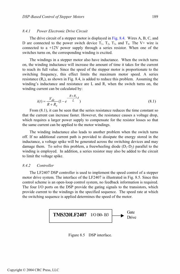
DSP-Based Control of Stepper Motors 189
8.4.1 Power Electronic Drive Circuit
The drive circuit of a stepper motor is displayed in Fig. 8.4. Wires A, B, C, and D are connected to the power switch device T1, T2, T3, and T4. The V+ wire is connected to a +12V power supply through a series resistor. When one of theswitches turns on, the corresponding winding is excited.
The windings in a stepper motor also have inductance. When the switch turnson, the winding inductance will increase the amount of time it takes for the currentto reach its full value. Since the speed of the stepper motor is proportionate to theswitching frequency, this effect limits the maximum motor speed. A seriesresistance (Rs), as shown in Fig. 8.4, is added to reduce this problem. Assuming thewinding’s inductance and resistance are L and R, when the switch turns on, thewinding current can be calculated by:
)1()(t
eRR
Vti LRR
s
dcs
(8.1)
From (8.1), it can be seen that the series resistance reduces the time constant so that the current can increase faster. However, the resistance causes a voltage drop, which requires a larger power supply to compensate for the resistor losses so that the same current can be applied to the motor windings.
The winding inductance also leads to another problem when the switch turnsoff. If no additional current path is provided to dissipate the energy stored in theinductance, a voltage spike will be generated across the switching devices and maydamage them. To solve this problem, a freewheeling diode (D1-D2) parallel to thewinding is employed. In addition, a series resistor may also be added to the circuitto limit the voltage spike.
8.4.2 Controller
The LF2407 DSP controller is used to implement the speed control of a steppermotor drive system. The interface of the LF2407 is illustrated in Fig. 8.5. Since this control scheme is an open-loop control system, no feedback information is required.The four I/O ports on the DSP provide the gating signals to the transistors, whichprovide current to the windings in the specified sequence. The speed rate at whichthe switching sequence is applied determines the speed of the motor.
I/O B0- B3 GateDriveTMS320LF2407
Figure 8.5 DSP interface.
Copyright © 2004 CRC Press, LLC

DSP-Based Control of Stepper Motors190
8.5 The Implementation of Stepper Motor Control System Using the
LF2407 DSP
The assembly code associated with the LF2407 was developed to implementthe open loop speed control system discussed previously. The flowchart for the DSP software is shown in Fig. 8.6.
NoYes
Start
Initialization procedure
Read commanded speed
Full step
Read full-stepsequence
Set I/O port
End
Output the program variables to DAC0~DAC3
Read half-stepsequence
Calculate the step Calculate the step
Figure 8.6 Flowchart of the stepper motor control algorithm.
It can be seen from Fig. 8.6 that the control algorithm of the stepper motordrive system consists of one main routine and includes four subroutine modules:
Initialization procedureSpeed control moduleOutput signals via I/O portDAC module
Only the speed control module is specific to the stepper motor control systemand will be dicussed in detail.
Copyright © 2004 CRC Press, LLC

DSP-Based Control of Stepper Motors 191
8.6 The Subroutine of Speed Control Module
The Timer 1 period interrupt is used for the speed control subroutine. Thissubroutine performs the task of reading the commanded speed and then convertingit to a pulse output on the I/O ports. Hence, the motor speed is determined by thetime interval of this interrupt. The block of assembly code below shows the Timer 1Interrupt Service Routine (ISR), which executes all subroutines upon everyinterrupt.
T1_ISR: NOP ;------------------*; Context Saving * ;------------------*;Context save regs
MAR *, AR1 ;AR1 is stack pointer MAR *+ ;skip one position SST #1, *+ ;save ST1 SST #0, *+ ;save ST0 SACH *+ ;save acc high SACL * ;save acc low POINT_EV
SPLK #0FFFFh , EVIFRA
POINT_B0
RUN_MODE POINT_B0CALL SPEED_PROFILE CALL VTIMER_SEC LACC STEP_FLG BCND HALF_MODE,GT CALL FULL_STEP B END_MODE
HALF_MODECALL HALF_STEP
END_MODECALL DAC_VIEW_Q15I
;------------------------------*;* Context restore and Return * ;------------------------------*END_ISR:
MAR *, AR1 ;make stack pointer active LACL *- ;Restore Acc low ADDH *- ;Restore Acc high LST #0, *- ;load ST0 LST #1, *- ;load ST1 POINT_PG0CLRC INTM RET
8.6.1 Full-Step Mode
Two-phase full-step mode described in Section 8.3.1 is implemented in the full-step subroutine as shown in the code on the next page. The commanded speed isconverted first to a pulse with a certain frequency in this routine. According to Table 8.2, the different sequence is read and then the corresponding I/O ports(IOPB0, 1, 2, 3 – A, B, C D) are set high/low to control the turn on/off of theswitches.
Copyright © 2004 CRC Press, LLC

DSP-Based Control of Stepper Motors 192
FULL_STEP: POINT_B0 ……POINT_B0LACC #MODE_FUL sub #3 BCND SET_MODE_FUL,NEQ SPLK #0,MODE_CNTL_FUL B FUL_EXIT ……RET
8.6.2 Half-Step Mode
Following the same procedure as described above, two-phase half-step mode strategy described in Section 8.3.2 is implemented in the code block shown below.
HALF_STEP: POINT_B0 POINT_B0……POINT_B0LACC MODE_CNTL_HLF sub #7 BCND SET_MODE_HLF,NEQ SPLK #0,MODE_CNTL_HLF B HLF_EXIT ……RET
Reference
1. Digital Signal Processing Control of Electric Machines and Drives Laboratory Manual, Department of Electrical Engineering, The Ohio State University, March 2002.
Copyright © 2004 CRC Press, LLC

Chapter 9
DSP-BASED CONTROL OF PERMANENT MAGNET BRUSHLESS DC
MACHINES
9.1 Introduction
Permanent magnet alternating current (PMAC) motors are synchronous motors
that have permanent magnets mounted on the rotor and poly-phase, usually three-
phase, armature windings located on the stator. Since the field is provided by the
permanent magnets, the PMAC motor has higher efficiency than induction or
switched reluctance motors. It also draws better power factor and has higher power
density. The advantages of PMAC motors, combined with a rapidly decreasing cost
of permanent magnets, have led to their widespread used in many variable-speed
drives such as robotic actuators, computer disk drives, domestic appliances,
automotive applications, and heating-ventilating-air conditioning (HVAC)
equipment.
In general, PMAC motors are categorized into two types. The first type of
motor is referred to as PM synchronous motor (PMSM). These motors produce a
sinusoidal back-EMF shown in Fig. 9.1(a), and should be supplied with sinusoidal
current/voltage. The PMSM’s electronic control and drive system uses continuous
rotor position feedback and pulse-width-modulation (PWM) to supply the motor
with the sinusoidal voltage or current. With this, constant torque is produced with
very little ripple. A detailed discussion of the PMSM drive system is given in
Chapter 12.
The second type of PMAC motor has a trapezoidal back-EMF and is referred to
as the brushless DC (BLDC) motor. The back-EMF of the BLDC motor is shown
in Fig. 9.1(b). The BLDC drive system is based on the feedback of rotor position,
which is not continuous as with the PMSM, but rather obtained at fixed points
typically every 60 electrical degrees for commutation of the phase currents. The
BLDC motor requires that quasi-rectangular shaped currents are fed into the
machine. Alternatively, the voltage may be applied to the motor every 1200, with a
current limit to hold the currents within the motor’s capabilities. Because the phase
currents are excited in synchronism with the constant part of the back-EMF,
constant torque is generated.
The objective of this chapter is to introduce the principles of the BLDC motor
control system, and then discuss the procedure of its implementation using the
LF2407 DSP.
193
Copyright © 2004 CRC Press, LLC

DSP-Based Control of Permanent Magnet Brushless DC Machines194
0 20 40 60 80 100 120 140 160 180-40
-30
-20
-10
0
10
20
30
40
Rotor Position (deg)
Ba
ck-E
MF
(V
)A B C
(a) Three-phase back-EMF of PMSM.
0 20 40 60 80 100 120 140 160 180-50
-40
-30
-20
-10
0
10
20
30
40
50
Rotor Position (deg)
Back-E
MF
(V
)
A B C
(b) Three-phase back-EMF of BLDC motors.
Figure 9.1 The back-EMF of PMAC motors.
Copyright © 2004 CRC Press, LLC

DSP-Based Control of Permanent Magnet Brushless DC Machines 195
9.2 Principles of the BLDC Motor
9.2.1 Mathematical Model
The phase variables are used to model the BLDC motor due to its non-
sinusoidal back-EMF and phase current. The terminal voltage equation of the
BLDC motor can be written as
(9.1)
c
b
a
c
b
a
s
s
s
c
b
a
e
e
e
i
i
i
pLR
pLR
pLR
v
v
v
.
00
00
00
where a, b, c are the phase voltages, ia, ib, ic are the phase currents, ea, eb, ec are
the phase back-EMF voltages, R is the phase resistance, Ls is the synchronous
inductance per phase and includes both leakage and armature reaction inductances,
and representspdt
d . The electromagnetic torque is given by
mccbbaae ieieieT / (9.2)
where m is the mechanical speed of the rotor. The equation of motion is
JBTTdt
dmLem /)( (9.3)
where TL is the load torque, B is the damping constant, and J is the moment of
inertia of the rotor shaft and the load.
9.3 Torque Generation
From (9.2), the electromagnetic torque of the BLDC motor is related to the
product of the phase back-EMF and current. The back-EMFs in each phase are
trapezoidal in shape and are displaced by 120 electrical degrees with respect to each
other in a three-phase machine. A rectangular current pulse is injected into each
phase so that current coincides with the crest of the back-EMF waveform, hence the
motor develops an almost constant torque. This strategy, commonly called six-step
current control, is illustrated by Fig. 9.2 and explained by (9.4). The amplitude of
each phase’s back-EMF is proportional to the rotor speed, and is given by
mkE (9.4)
where k is a constant and depends on the number of turns in each phase, is the
permanent magnet flux, and m is the mechanical speed. In Fig. 9.2, during any
1200 interval, the instantaneous power converted from electrical to mechanical is the
sum of the contributions from two phases in series, and is given by
EITP emo 2 (9.5)
where is the output torque andeT I is the amplitude of the phase current. From
(9.4) and (9.5), the expression for output torque can be written as
IkIkT te 2 (9.6)
where is the torque constant. Since the electromagnetic torque is only
proportional to the amplitude of the phase current in (9.6), torque control of the
BLDC motor is essentially accomplished by phase current control.
tk
Copyright © 2004 CRC Press, LLC

DSP-Based Control of Permanent Magnet Brushless DC Machines196
t
t
t
t
t
t
t
t
t
E
Ec
ia
ib
ic
T1
T2
T3
T4
T5
T6
3
0
6
00
1
20
15
0
9
0
2
10
24
0
18
0
30
0
33
0
27
0
36
0
Ea
b
Torque
t
Power switches(T1-T6) turn on
Figure 9.2 The principle of the six-step current control algorithm.
T1-T6 are the gate signals, Ea , Eb , and Ec are the motor phase back-EMF, Ia, Ib, and
Ic are the motor phase currents.
9.4 BLDC Motor Control System
Based on the previously discussed concept, a BLDC motor drive system is
shown in Fig. 9.3. It can be seen that the total drive system consists of the BLDC
motor, power electronics converter, sensor, and controller. These components are
discussed in detail in the following sections.
9.4.1 BLDC Machine
BLDC motors are predominantly surface-magnet machines with wide magnet
pole-arcs. The stator windings are usually concentrated windings, which produce a
square waveform distribution of flux density around the air-gap. The design of the
BLDC motor is based on the crest of each half-cycle of the back-EMF waveform.
In order to obtain smooth output torque, the back-EMF waveform should be wider
than 120 electrical degrees. A typical BLDC motor with 12 stator slots and 4 poles
on the rotor is shown in Fig. 9.4.
Copyright © 2004 CRC Press, LLC

DSP-Based Control of Permanent Magnet Brushless DC Machines 197
D1
D2D4
D3
C
T1
T4
T3
T6
T5
T2
Ld
V
s
BLDC
motor
Hall sensor
signal
controller
current
to T1~T6
ab
c
Figure 9.3 BLDC motor control system.
Magnet
Iron Core
ConcentratedWindings
Rotor
Figure 9.4 The 4-pole 12-slot BLDC motor.
9.4.2 Power Electronic Converter
As shown in Fig. 9.3, the power electronic converter in the BLDC motor drive
system consists of two parts: a front-end rectifier and a three-phase full-bridge
inverter. The front-end rectifier is usually a full-bridge diode rectifier unless a
switching rectifier is used to provide regeneration capability.
The inverter is usually responsible for the electronic commutation and current
regulation. For the six-step current control, if the motor windings are Y connected
without the neutral connection, only two of the three phase currents flow through
the inverter in series. This results in the amplitude of the DC link current always
being equal to that of the phase currents. As far as the inverter goes, there are only
two switches per leg, one upper and one lower switch which conduct at any
moment. PWM current controllers are typically used to regulate the actual machine
Copyright © 2004 CRC Press, LLC

DSP-Based Control of Permanent Magnet Brushless DC Machines198
currents in order to match the rectangular current reference waveforms shown in
Fig. 9.2. For example, during one 60o interval when switches T1 and T6 are active,
phases A and B conduct. The lower switch T6 is always turned on and the upper
switch T1 is chopped on/off using either a hysteresis current controller with variable
switch frequency or a PI controller with fixed switch frequency. When T1 and T6
are conducting, current builds up in the path shown in the dashed line of Fig. 9.5(a).
When switch T1 is turned off, the current decays through diode D4 and switch T6 as
shown in the dashed line of Fig. 9.5(b). In the next interval, switch T2 is on, and T1
is chopped so that phase A and phase C conduct. During the commutation interval,
the phase B current rapidly decreases through the freewheeling diode D3 until it
becomes zero and the phase C current builds up.
From the above analysis, each of the upper switches is always chopped for one
1200 interval and the corresponding lower switch is always turned on per interval.
The freewheeling diodes provide the necessary paths for the currents to circulate
when the switches are turned off and during the commutation intervals.
9.4.3 Sensors
There are two types of sensors for the BLDC drive system: a current sensor and
a position sensor. Since the amplitude of the dc link current is always equal to that
of the motor phase current in six-step current control, the dc link current is
measured instead of the phase current. Thus, a shunt resistor, which is in series with
the inverter, is usually used as the current sensor. Hall-effect position sensors
typically provide the position information needed to synchronize the stator
excitation with rotor position in order to produce constant torque. Hall-effect
sensors detect the change in magnetic field. The rotor magnets are used as triggers
for the Hall sensor. A signal conditioning circuit integrated within the Hall switch
provides a TTL-compatible pulse with sharp edges and high noise immunity for
connection to the controller.
For the six-step current control algorithm, rotor position needs to be detected at
only six discrete points in each electrical cycle. The controller tracks these six
points so that the proper switches are turned on or off for the correct intervals.
Three Hall-effect sensors, spaced 120 electrical degrees apart, are mounted on the
stator frame. The digital signals from the Hall sensors are then used to determine
the rotor position and switch gating signals for the inverter switches.
Copyright © 2004 CRC Press, LLC
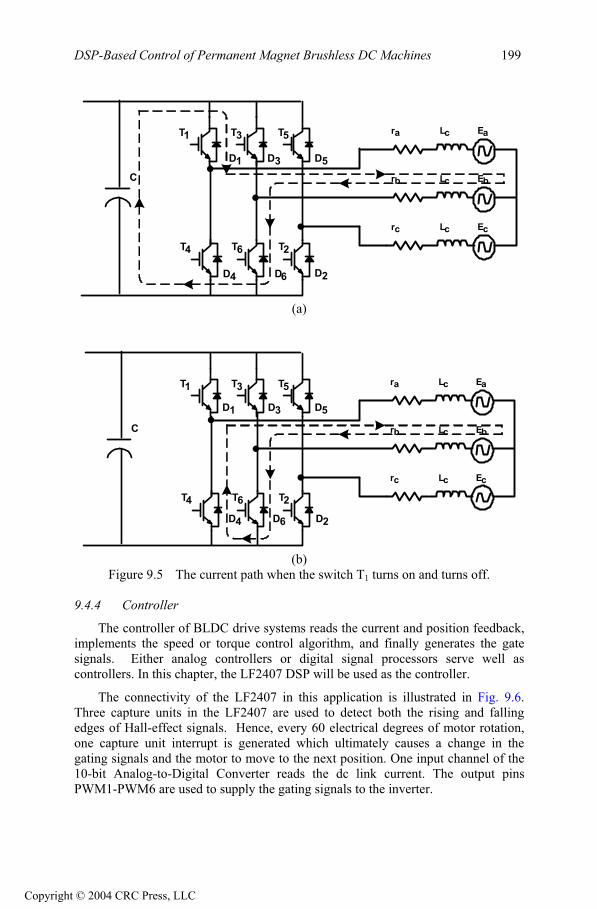
DSP-Based Control of Permanent Magnet Brushless DC Machines 199
C
T4 T6 T2
ra Lc Ea
rb Lc Eb
rc Lc Ec
T3 T5T1
D1 D3 D5
D2D6D4
(a)
C
T6 T2
ra Lc Ea
rb Lc Eb
rc Lc Ec
T1 T3 T5
T4
D1 D3 D5
D2D6D4
(b)
Figure 9.5 The current path when the switch T1 turns on and turns off.
9.4.4 Controller
The controller of BLDC drive systems reads the current and position feedback,
implements the speed or torque control algorithm, and finally generates the gate
signals. Either analog controllers or digital signal processors serve well as
controllers. In this chapter, the LF2407 DSP will be used as the controller.
The connectivity of the LF2407 in this application is illustrated in Fig. 9.6.
Three capture units in the LF2407 are used to detect both the rising and falling
edges of Hall-effect signals. Hence, every 60 electrical degrees of motor rotation,
one capture unit interrupt is generated which ultimately causes a change in the
gating signals and the motor to move to the next position. One input channel of the
10-bit Analog-to-Digital Converter reads the dc link current. The output pins
PWM1-PWM6 are used to supply the gating signals to the inverter.
Copyright © 2004 CRC Press, LLC
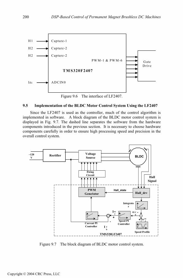
DSP-Based Control of Permanent Magnet Brushless DC Machines200
Capture-1
Capture-2
PW M -1 & PW M -6
T M S320F2407
H 1
H 2
Idc AD CIN 0
Capture-2H 2
G ate
Drive
Figure 9.6 The interface of LF2407.
9.5 Implementation of the BLDC Motor Control System Using the LF2407
Since the LF2407 is used as the controller, much of the control algorithm is
implemented in software. A block diagram of the BLDC motor control system is
displayed in Fig. 9.7. The dashed line separates the software from the hardware
components introduced in the previous section. It is necessary to choose hardware
components carefully in order to ensure high processing speed and precision in the
overall control system.
BLDC
Firing
Circuit
RectifierVoltage
Source~120
V
Integrato
r
Current PI
Controller
Speed PI
Controller
PWM
Generator
Hall
Signal
Hall_drvHall_state
f
b-
+
TMS320LF2407
Ire
f
I f
b
-
+
Speed Profile
re
f
Figure 9.7 The block diagram of BLDC motor control system.
Copyright © 2004 CRC Press, LLC

DSP-Based Control of Permanent Magnet Brushless DC Machines 201
The overall control algorithm of the BLDC motor consists of nine modules:
1. Initialization procedure
2. Detection of Hall effect signals
3. Speed control subroutine
4. Measurement of current
5. Speed profiling
6. Calculation of actual speed
7. PID regulation
8. PWM generation
9. DAC output
The flowchart of the overall control algorithm is illustrated in Fig. 9.8.
No
Yes
Start
Initialization procedure
Read DC link currentdcI ; Load Hall Effect signals
Execute
speed loop?
Read reference speed ref
Read Hall
sensor signal
End
Calculate the motor actual speedr
Speed PI regulator
Calculate the commended torque
Calculate the command DC link current*
dci using (12.6)
Current PI regulator
Generate the PWM using generator
End
Output the program variables to DAC0~DAC3
Figure 9.8 BLDC algorithm flowchart.
Copyright © 2004 CRC Press, LLC

DSP-Based Control of Permanent Magnet Brushless DC Machines202
In the follwing sections, each block of the flow chart is dicussed in detail and
the corresponding assembly code is given.
9.5.1 Initialization Procedure
The initialization procedures include the initialization of registers, memory
allocations, and initializing constants and system variables. The TI website
(www.ti.com) provides the standard linker command file for memory allocation on
the LF2407. Readers can simply download it and then modify this file according to
their own needs.
The need for and the initialization of system variables vary according to the
application. The variables used in the BLDC control algorithm to generate the speed
profile are initialized below:
POINT_B0SPLK #0, SPD_CNT SPLK #0, VTS_SEC SPLK #0, VTS_CNT SPLK #0, STEP_1 SPLK #5, VTS_PRESCALE SPLK
#PSTEP_1, PROFILE_STEP_PTR SPLK #04D0H, SPD_SCALESPLK #0fffh, SPD DESIRED
For BLDC motor control, the register initializations include four parts: system
interrupt initialization, initialization of the ADC module, initialization of the Hall-
effect signal detected, and initialization of the Event Manager. The assembly code
for system interrupt initialization is given below:
;System Interrupt Init. ;Event Manager POINT_EV
SPLK #0000001000000000b, EVIMRA;Enable T1 Underflow Int (i.e. Period)
SPLK #0000000000000111b, EVIMRC ;Enable CAP1,2,3 intsSPLK #0FFFFh, EVIFRA
;Clear all Group A interrupt flags SPLK #0FFFFh, EVIFRB
;Clear all Group B interrupt flags SPLK #0FFFFh,EVIFRC
;Clear all Group C interrupt flags POINT_PG0
SPLK #0000000000001010b,IMR ;En Int lvl 2,4 (T2 & CAP ISR)
SPLK #0FFFFh, IFR ;Clear any pending Ints
9.5.2 The Detection of Hall-Effect Signals
Each edge of the Hall-effect sensor output signal generates a capture interrupt.
The CPU responds to this interrupt and branches to the interrupt service subroutine
to perform the following tasks: detect the Hall sensor sequences, decode the
sequence, define the six states of the inverter, and record the time interval between
Copyright © 2004 CRC Press, LLC

DSP-Based Control of Permanent Magnet Brushless DC Machines 203
the two nearest Hall-effect edges. The time between edges is used to calculate the
rotor speed. The assembly code for the interrupt service subroutine is given below:
CAP_ISR:;Context save regs
MAR *, AR1 ;AR1 is stack pointer MAR *+ ;skip one position SST #1, *+ ;save ST1 SST #0, *+ ;save ST0 SACH *+ ;save acc high SACL * ;save acc low CALL HALL3_DRV
;Restore Context END_ISR:
MAR *, AR1 ;make stack pointer active LACL *- ;Restore Acc low ADDH *- ;Restore Acc high LST #0, *- ;load ST0 LST #1, *- ;load ST1 CLRC INTM RET
The following code determines which one of the six switching states is needed:
HALL3_DRV:……
Map_States:LDP #hall_vars LACC hall_seq, 2 ;x4 for jump table ADD #STATE_TABLE BACC
STATE_TABLE: ;Map Hall connections and readings to;BLDC_PWM_DRV's states based on it's
;state 0 alignmentSPLK #1, hall_state_next ;seq=0, BLDC_PWM_DRV next state 1 B HALL_ENDSPLK #3, hall_state_next ;seq=1, BLDC_PWM_DRV next state 3 B HALL_ENDSPLK #2, hall_state_next ;seq=2, BLDC_PWM_DRV next state 2 B HALL_ENDSPLK #5, hall_state_next ;seq=3, BLDC_PWM_DRV next state 5 B HALL_ENDSPLK #0, hall_state_next ;seq=4, BLDC_PWM_DRV next state 0 B HALL_ENDSPLK #4, hall_state_next ;seq=5, BLDC_PWM_DRV next state 4
HALL_END: RET
9.5.3 The Subroutine of Speed Control Algorithm
The Timer 1 underflow interrupt is used for the speed control subroutine. The
speed control subroutine performs the task of reading the current, loading the
inverter state obtained from capture interrupt, generating the commanded speed
profile, calculating the actual motor speed, regulating speed and current, and finally
generating the PWM signals to drive the inverter. The PWM frequency is
determined by the time interval of this interrupt; the duty cycle is recalculated in
every interrupt. The speed control algorithm is implemented by the following
assembly code:
Copyright © 2004 CRC Press, LLC

DSP-Based Control of Permanent Magnet Brushless DC Machines204
T1_PERIOD_ISR:;Context save regs
MAR *, AR1 ;AR1 is stack pointer MAR *+ ;skip one position SST #1, *+ ;save ST1 SST #0, *+ ;save ST0 SACH *+ ;save acc high SACL * ;save acc low POINT_EVSPLK #0FFFFh,EVIFRA ;Clear all Group A interrupt
flags (T1 ;ISR) READ_HALL
LDP #hall_vars Lacc hall_state_next POINT_B0sacl cmtn_ptr_bd ;Input to BLDC_PWM_DRV
CUR_READCALL AD_CONV POINT_B0LACC CL_SPD_FLG BCND CURRENT_CNTL,GT ;speed-loop?
;speed controlSPEED_CNTL: POINT_B0
CALL SPEED_PROFILE CALL VTIMER_SEC CALL SPEED_CAL CALL D_PID_spd LACC D_spd_out SACL I_ref
;current controlCURRENT_CNTL
CALL D_PID_cur LACC D_cur_out SACL D_func
PWM_GEN CALL BLDC_PWM_DRVDA_CONV CALL DAC_VIEW_Q15I
;Restore ContextEND_ISR:
MAR *, AR1 ;make stack pointer active LACL *- ;Restore Acc low ADDH *- ;Restore Acc high LST #0, *- ;load ST0 LST #1, *- ;load ST1 CLRC INTM RET
9.5.4 Measurement of the Current (ADC Module)
For the BLDC motor control algorithm, the ADC converter reads in the voltage
across the shunt resistor on ADCIN0. This voltage is proportional to the dc link
current because the resistor is in series with the flow of current. The code section
below reads the result register and obtains the ADC conversion result of the voltage
across the shunt resistor.
AD_CONVLDP #ADCTRL1>>7 LACC ADC_RESULT0 SFRAND #7FFFh SACL Idc ….….
AD_EXIT RET
Copyright © 2004 CRC Press, LLC

DSP-Based Control of Permanent Magnet Brushless DC Machines 205
9.5.5 Profile of the Reference Speed
The reference speed profile is used to control the dynamic response and steady
state behavior of the motor. The speed profile is divided into different sections,
such as the acceleration interval, constant speed interval, and deceleration interval.
We can use the different intervals to make the rotor accelerate, run at constant
speed, or decelerate. One example of speed profile is shown in Fig. 9.8.
Speed-1
Speed-2
Speed-1
time
1st Cycle 2nd Cycle
t3 t4 t5=Tp Tp+t2t2t1
Speed-2
Tp+t3 Tp+t4
Figure 9.8 Speed profile.
In the speed profile given in Fig. 9.8, the interval from time 0 to t1 represents a
soft-start period where reference speed is slowly increased from zero to speed-1.
For the time interval between t1 to t2, the speed reference is maintained constant at
its value, speed-1. During the time interval from t2 to t3, the reference speed is
slowly reduced to speed-2. The reference speed is then kept constant at speed-2 for
the time interval from t3 to t4. Finally, the speed is again increased to speed-1 over
the time interval t4 to t5. In our case, the sequence t2 to t5 is repeated continuously
unless disabled by another routine. A sample of the assembly code used for such a
speed profile is given below:
SPEED_PROFILE: …. …. PSTEP_4 LACC #SPEED_4
AND #0fFFH SACL speed_ref LACC SPD_CNTSUB #03fFHBCND GO_STEP5,GTLACC VTS_SEC SUB #TLENGTH_4 BCND SPR_END,LT SPLK #0,VTS_SEC ;RESET VIRTUAL TIMER SPLK #0,VTS_CNTLACC SPD_CNT ADD #1SACL SPD_CNTB SPR_END
GO_STEP5 SPLK#0,VTS_SEC ;RESET VIRTUAL TIMER SPLK #0,VTS_CNT SPLK #01ffH,STEP_3 SPLK #0,SPD_CNT LACC #PSTEP_5 SACL PROFILE_STEP_PTR B SPR_END …..
SPR_END RET
Copyright © 2004 CRC Press, LLC

DSP-Based Control of Permanent Magnet Brushless DC Machines206
9.5.6 The Calculation of the Actual Motor Speed
This module uses the value of the variable Timestamp, which represents the
time interval between the two edges of the Hall-effect signal generated by the
position interface module, to calculate the motor shaft speed. With a 30 MHz
system clock as in the case of LF2407, Timestamp is related to the motor speed by
910332
60
prescalarTimestamp
m
(9.7)
m0.59066553632
_Timestamp
calspeed (9.8)
where
m = shaft speed in rpm.
prescalar = prescalar value for Timer-2 = 128
tcpu = CPU period = 33 nsec
speed_cal = calculated speed in rpm
The speed calculation routine measures the time between two consecutive edge
transitions of the position signal and cannot distinguish between the directions of
rotation. A portion of the assembly code of the speed calculation routine is given
below:
SPEED_CAL:….….LT RES ;RES=1/TimestampMPY SPD_SCALE PACSACH speed_cal, 4RET
9.5.7 PID (Proportional, Integral, and Derivative) Regulation
PID controllers are used for both speed and current regulation. Both types of
controllers have the same structure. The rectangular (trapezoidal) method of
integration is used and depends upon the value of the parameters K1, K2, and K3.
Limits are set to limit the output of PI controller. This routine implements the
following PI equation:
)2()1()()2()( 321 neKneKneKnUnU (9.9)
where
is the current output of the PI controller (n)(nU th sample)
is the output of PI controller at (n-2))2(nU th sample
is the error at n)(ne th sample
is the error at (n-1))1(ne th sample
is the error at (n-2))2(ne th sample
Copyright © 2004 CRC Press, LLC

DSP-Based Control of Permanent Magnet Brushless DC Machines 207
The constants , , and for trapezoidal approximation are 1K 2K 3K
221
TK
T
KKK id
p (9.10)
T
KTKK d
i 42 (9.11)
T
TKKKK i
pd23 (9.12)
and for rectangular approximation are
TKT
KKK i
dp1 (9.13)
T
KTKK d
i 22 (9.14)
pd K
T
KK3 (9.15)
In all of the above equations Kp, Kd, Ki are defined as in
dt
deKdtKteKtu dip )()( (9.16)
A portion of the assembly code implementing the PI controller is given below:
D_PID_spd:….….LACC D_Un_H_0SUB #MAX_POS_LIMITBCND D_PLUS_OK,LEQ ;If maxed out, saturate at max -veSPLK #MAX_POS_LIMIT,D_Un_H_0 SPLK #0,D_Un_L_0 B D_EXIT
D_PLUS_OK: LACC D_Un_H_0 ;else keep current value SUB #MAX_NEG_LIMIT BCND D_NEG_OK,GEQ ;if maxed out, saturate at max +ve SPLK #MAX_NEG_LIMIT,D_Un_H_0 ;Saturation control SPLK #0,D_Un_L_0
D_NEG_OK:…..…..RET
9.5.8 PWM Generation
The Compare Units have been used to generate the PWM signals. The PWM
output signal is high when the output of current PI regulation matches the value of
T1CNT and is set to low when the timer underflow occurs. The switch states are
controlled by the ACTR register. As discussed earlier, in order to minimize the
switching loss, the lower switches are always kept on and the upper switches are
chopped on/off to regulate the phase current. From the implementation point of
Copyright © 2004 CRC Press, LLC

DSP-Based Control of Permanent Magnet Brushless DC Machines 208
view, in using the LF2407, it is required that the ACTR register be reset for each
interval. In other words, PWM1, PWM3, and PWM5 which gate the upper switches
are set as active low/high and PWM2, PWM4, and PWM6 which trigger the lower
switches are set as force high. The sample of code below illustrates this
implementation.
BLDC_PWM_DRV….
LACC #COMMUTATION_TBL ADD cmtn_ptr_bd TBLR GPR0 LACC GPR0 BACCSTATE_ANB ;Input current path, Phase A POINT_EV ;Output current path, Phase B SPLK #00C2H, ACTR ;Non fed phase, Phase C B STATE_END ….
STATE_END …. RET
9.5.9 DAC Module
The LF2407 evaluation board contains four channels DAC. In this application,
the DAC on the evaluation board is used to display various system variables to be
seen on an oscilloscope in real time. This feature is very useful during the
development stage for real time debugging and verification of the software. The
code below accepts the address pointers for four different system variables and then
automatically updates the DAC channels to reflect the change in these variables.
;Convert Q15 input value to an absolute Q0 output to DAC0 channel POINT_B0SPM 1 MAR *, AR6 LAR AR6, DAC_IPTR0 LT * MPY dac_hlf_rng ;Normalize to half range of DAC PAC ADDH dac_hlf_rng ;offset by 1/2 DAC max value SACH GPR0 OUT GPR0, PA0 ;DAC0 o/p
Copyright © 2004 CRC Press, LLC
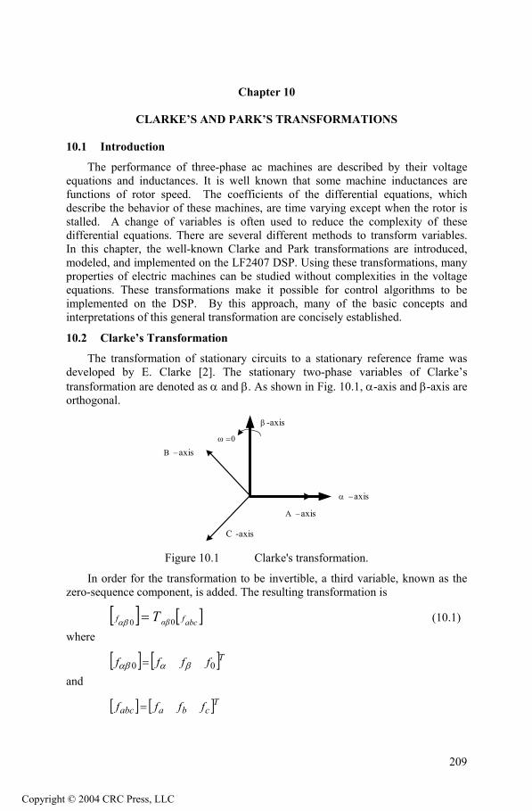
Chapter 10
CLARKE’S AND PARK’S TRANSFORMATIONS
10.1 Introduction
The performance of three-phase ac machines are described by their voltage equations and inductances. It is well known that some machine inductances are functions of rotor speed. The coefficients of the differential equations, which describe the behavior of these machines, are time varying except when the rotor is stalled. A change of variables is often used to reduce the complexity of these differential equations. There are several different methods to transform variables. In this chapter, the well-known Clarke and Park transformations are introduced, modeled, and implemented on the LF2407 DSP. Using these transformations, many properties of electric machines can be studied without complexities in the voltage equations. These transformations make it possible for control algorithms to be implemented on the DSP. By this approach, many of the basic concepts and interpretations of this general transformation are concisely established.
10.2 Clarke’s Transformation
The transformation of stationary circuits to a stationary reference frame was developed by E. Clarke [2]. The stationary two-phase variables of Clarke’s transformation are denoted as α and β. As shown in Fig. 10.1, α-axis and β-axis are orthogonal.
β -axis
α −axis
Α −axis
C -axis
Β −axisω =0
Figure 10.1 Clarke's transformation.
In order for the transformation to be invertible, a third variable, known as the zero-sequence component, is added. The resulting transformation is
(10.1) [ ] [ ]abcfαβf Τ 00 =αβ
where
[ ] [ Tffff 00 βααβ = ]and
[ ] [ ]Tcbaabc ffff =
209
Copyright © 2004 CRC Press, LLC

Clarke’s and Park’s Transformations 210
where represents voltage, current, flux linkages, or electric charge fand the transformation matrix, , is given by 0αβT
−
−−
=
21
21
21
23
230
21
211
32
0αβT (10.2)
The inverse transformation is given by
(10.3) [ ] [ ]01
0 αβαβ fTfabc−=
where the inverse transformation matrix is presented by
−−
−=−
123
21
123
21
1011
0αβT (10.4)
10.3 Park’s Transformation
In the late 1920s, R.H. Park [1] introduced a new approach to electric machine analysis. He formulated a change of variables which replaced variables such as voltages, currents, and flux linkages associated with fictitious windings rotating with the rotor. He referred the stator and rotor variables to a reference frame fixed on the rotor. From the rotor point of view, all the variables can be observed as constant values. Park’s transformation, a revolution in machine analysis, has the unique property of eliminating all time varying inductances from the voltage equations of three-phase ac machines due to the rotor spinning.
Although changes of variables are used in the analysis of ac machines to eliminate time-varying inductances, changes of variables are also employed in the analysis of various static and constant parameters in power system components. Fortunately, all known real transformations for these components are also contained in the transformation to the arbitrary reference frame. The same general transformation used for the stator variables of ac machines serves the rotor variables of induction machines. Park’s transformation is a well-known three-phase to two-phase transformation in synchronous machine analysis. Park’s transformation is presented in Fig. 10.2.
Copyright © 2004 CRC Press, LLC

Clarke’s and Park’s Transformations 211
A -axis
C -axis
B -axisω
q
q -axis
d -axis
Figure 10.2 Park's transformation.
The transformation equation is of the form
[ ] [ ]abcsqdsqd fTf )(00 θ= (10.5) where
[ ] [ ]Tsdsqssqd ffff 00 =
and [ ] [ Tcsbsasabcs ffff = ]
and the dq0 transformation matrix is defined as
+−
+−
=
21
21
21
)3
2sin()3
2sin()sin(
)3
2cos()3
2cos()cos(
32)(0
πθπθθ
πθπθθ
θsqdT (10.6)
θ is the angular displacement of Park’s reference frame and can be calculated by
(10.7) )0()(0
θζζωθ += ∫t
d
where ζ is the dummy variable of integration. It can be shown that for the inverse transformation we can write
[ ] [ ]sqdqdabcs fTf 01
0 )( ⋅= −θ (10.8) where the inverse of Park’s transformation matrix is given by
Copyright © 2004 CRC Press, LLC

Clarke’s and Park’s Transformations 212
++
−−=−
1)3
2sin()3
2cos(
1)3
2sin()3
2cos(
1)sin()cos(
)( 10
πθπθ
πθπθ
θθ
θqdT (10.9)
In the previous equations, the angular displacement θ must be continuous, but the angular velocity associated with the change of variables is unspecified. The frame of reference may rotate at any constant, varying angular velocity, or it may remain stationary. The angular velocity of the transformation can be chosen arbitrarily to best fit the system equation solution or to satisfy the system constraints. The change of variables may be applied to variables of any waveform and time sequence; however, we will find that the transformation given above is particularly appropriate for an a-b-c sequence.
10.4 Transformations Between Reference Frames
In order to reduce the complexity of some derivations, it is necessary to transform the variables from one reference frame to another one. To establish this transformation between any two reference frames, we can denote y as the new reference frame and x as the old reference frame. Both new and old reference frames are shown in Fig. 10.3.
ωy
θx
qy -axis
dy -axis
ωx
θy
qx -axis
dx -axis
Figure 10.3 Transformation between two reference frames.
It is assumed that the reference frame x is rotating with angular velocity ωx and the reference frame y is spinning with the angular velocity ωy. θx and θy are angular displacements of reference frames x and y, respectively. In this regard, we can rewrite the transformation equation as
[ ] [ ]sqdyxsqd
ysqd ff T 000 ⋅= → (10.10)
Copyright © 2004 CRC Press, LLC

Clarke’s and Park’s Transformations 213
But we have
(10.11)
⋅=
fTf abcs
xsqd
xsqd 00
If we substitute (10.11) in (10.10) we get
(10.12)
⋅⋅=
→ fTTf abcs
xsqd
yxsqd
ysqd 000
In another way, we can find out that
(10.13)
⋅=
fTf abcs
ysqd
ysqd 00
From (10.12) we obtain
(10.14) 1
000−→ ⋅= TTT x
sqdy
sqdyxsqd
Then, the desired transformation can be expressed by the following matrix:
(10.15)
−−−−−
=→
1110)cos()sin(0)sin()cos(
0 θθθθθθθθ
xyxyxyxy
T yxsqd
10.5 Field Oriented Control (FOC) Transformations
In the case of FOC of electric machines, control methods are performed in a two-phase reference frame fixed to the rotor (qr-dr) or fixed to the excitation reference frame (qe-de). We want to transform all the variables from the three-phase a-b-c system to the two-phase stationary reference frame and then retransform these variables from the stationary reference frame to a rotary reference frame with arbitrary angular velocity of ω. These transformations are usually cascaded. The block diagram of this procedure is shown in Fig. 10.4.
cba −−
dq ss − ee dq −
MachineModel in
ee dq −
eθcos eθsin
eqf
edf
Machine
af
bf
cf
dq ss −s
qf
sdf
Figure 10.4 Machine side transformation in field oriented control.
Copyright © 2004 CRC Press, LLC

Clarke’s and Park’s Transformations 214
In this figure, f denotes the currents or voltages and qe-de represents the arbitrary rotating reference frame with angular velocity ωe and qs-ds represents the stationary reference frame. In the vector control method, after applying field- oriented control it is necessary to transform variables to stationary a-b-c system. This can be achieved by taking the inverse transformation of variables from the arbitrary rotating reference frame to the stationary reference frame and then to the a-b-c system. The block diagram of this procedure is shown in Fig. 10.5. In this block diagram, * is a representation of commanded or desired values of variables.
ee dq −
cba −−
eθcos eθsin
*eqf
*edf
Control
*sqf
*sdf
f a*
f b*
f c*
dq ss −
dq ss −
Figure 10.5 Variable transformation in the field oriented control.
10.6 Implementing Clarke’s and Park’s Transformations on the LF240X
10.6.1 Implementing Clarke’s Transformation
It is desired to transfer the three-phase stationary parameters , , and from the
af bf cf a-b-c system to the two-phase stationary reference frame. It is assumed that
the system is balanced and we have
(10.16) 0=++ cba fffWe can rewrite (10.1) as follows:
cba ffff31
31
32
−−=α (10.17)
)(3
1cb fff −=β (10.18)
Substituting cf from (10.16) into (10.17) and (10.18) results in
(10.19) aff =α
Copyright © 2004 CRC Press, LLC

Clarke’s and Park’s Transformations 215
)2(3
1ba fff +=β (10.20)
10.6.1.1 Inputs and Outputs of Clarke’s Transformation Block
The inputs and outputs of Clarke’s transformation are shown in Fig. 10.6. As it is shown in this figure, and are inputs and and are outputs of this transformation.
af bf αf βf
CLARKETRANSFORMATION
fa
fb
fα
fβ
Q15 Format
Q15 Format
Q15 Format
Q15 Format Figure 10.6 Clarke transformation.
To enjoy better resolution of the variables in fixed point DSP, we transfer all variables to the Q15-based format. With this consideration, the maximum value of inputs and outputs can be (215-1) or in hexadecimal, the format shall be 7FFFh. In this base, the variables can vary in the range 8000h-7FFFh. This transformation converts balanced three-phase quantities into balanced two-phase quadrature quantities as shown in Fig. 10.7.
Figure 10.7 Quantities in Clarke's transformation. (Courtesy of Texas
Instruments)
As we previously noted, our calculations are based on the Q15 format . So all
the coeficients are present in this representation. Then 1/√3 is represented by LDP #sqrt3inv ;sqrt3inv=(1/sqrt(3)) ;=0.577350269 SPLK #018830,sqrt3inv ;1/sqrt(3) (Q15)
Copyright © 2004 CRC Press, LLC

Clarke’s and Park’s Transformations 216
Clarke’s transformation is implemented as follows: SETC SXM ;Sign extension mode on LDP #clark_a ;clark_alfa = clark_a LACC clark_a ;ACC = clark_a SACL clark_alfa ;clark_d = clark_a ;clark_beta=(2*clark_b+clark_a)/ ;sqrt(3) SFR ;ACC = clark_a/2 ADD clark_b ;ACC = clark_a/2 + clark_b SACL clk_temp ;clk_temp = clark_a/2 + clark_b LT clk_temp ;TREG = clark_a/2 + clark_b MPY sqrt3inv ;PREG=(clark_a/2+clark_b)* ;(1/sqrt(3)) PAC ;ACC=(clark_a/2+clark_b)* ;(1/sqrt(3)) SFL ;ACC=(clark_a+clark_b*2)* ;(1/sqrt(3)) SACH clark_beta ;clark_beta=(clark_a+clark_b*2 ;(1/sqrt(3)) SPM 0 ;SPM reset RET
10.6.2 Inverse Clarke’s Transformation
From (10.3), the inverse Clarke functions for a balanced system can be obtained as
23
23
βα
βα
α
fff
fff
ff
c
b
a
∗−−=
∗+−=
=
(10.21)
This transformation converts balanced two-phase quadrature quantities into balanced three-phase quantities. The block diagram of the inverse Clarke transformation is shown in Fig. 10.8.
Figure 10.8 Inverse Clark transformation block.
In this block diagram, αf and are inputs and , , and are outputs.
Inputs and outputs are represented in Q15 format. Variation of quantities in the inverse Clark transformation is shown in Fig. 10.9.
βf af bf cf
Copyright © 2004 CRC Press, LLC
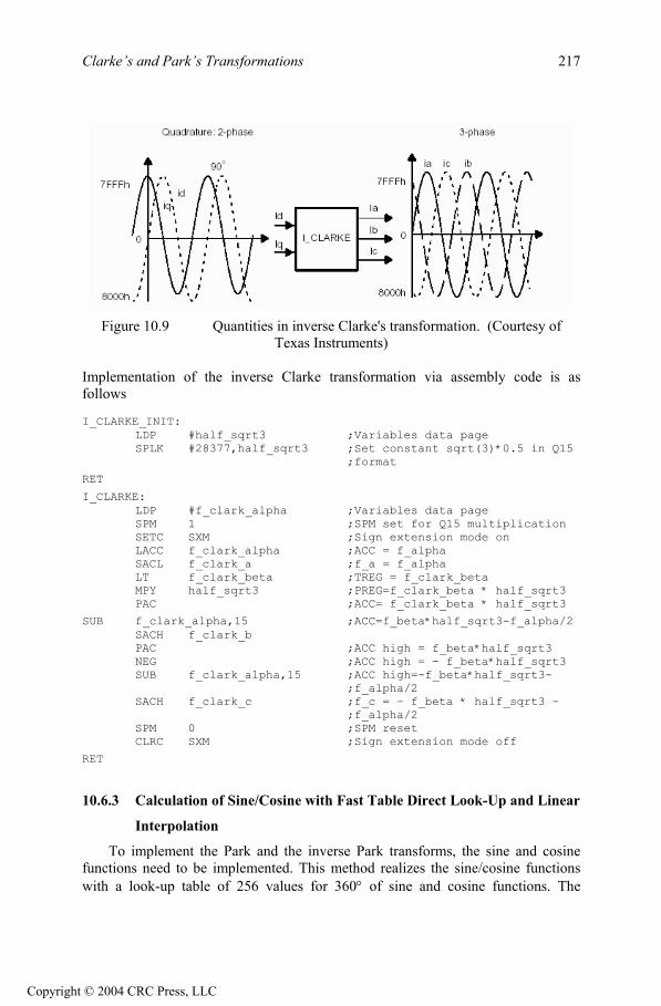
Clarke’s and Park’s Transformations 217
Figure 10.9 Quantities in inverse Clarke's transformation. (Courtesy of
Texas Instruments) Implementation of the inverse Clarke transformation via assembly code is as follows
I_CLARKE_INIT: LDP #half_sqrt3 ;Variables data page SPLK #28377,half_sqrt3 ;Set constant sqrt(3)*0.5 in Q15 ;format
RET
I_CLARKE: LDP #f_clark_alpha ;Variables data page SPM 1 ;SPM set for Q15 multiplication SETC SXM ;Sign extension mode on LACC f_clark_alpha ;ACC = f_alpha SACL f_clark_a ;f_a = f_alpha LT f_clark_beta ;TREG = f_clark_beta MPY half_sqrt3 ;PREG=f_clark_beta * half_sqrt3 PAC ;ACC= f_clark_beta * half_sqrt3
SUB f_clark_alpha,15 ;ACC=f_beta*half_sqrt3-f_alpha/2 SACH f_clark_b PAC ;ACC high = f_beta*half_sqrt3 NEG ;ACC high = - f_beta*half_sqrt3 SUB f_clark_alpha,15 ;ACC high=-f_beta*half_sqrt3- ;f_alpha/2 SACH f_clark_c ;f_c = - f_beta * half_sqrt3 – ;f_alpha/2 SPM 0 ;SPM reset CLRC SXM ;Sign extension mode off
RET
10.6.3 Calculation of Sine/Cosine with Fast Table Direct Look-Up and Linear
Interpolation
To implement the Park and the inverse Park transforms, the sine and cosine functions need to be implemented. This method realizes the sine/cosine functions with a look-up table of 256 values for 360° of sine and cosine functions. The
Copyright © 2004 CRC Press, LLC

Clarke’s and Park’s Transformations 218
method includes linear interpolation with a fixed step table to provide a minimum harmonic distortion. This table is loaded in program memory. The sine value is presented in Q15 format with the range of -1<value<1. The first few rows of the look-up sine table are presented as follows:
;SINVALUE ; Index Angle Sin(Angle)
---------------- -------- -------- ------------
SINTAB_360
.word 0 ; 0 0 0.0000
.word 804 ; 1 1.41 0.0245
.word 1608 ; 2 2.81 0.0491
.word 2410 ; 3 4.22 0.0736
.word 3212 ; 4 5.63 0.0980
The following assembly code is written to read values of sine from the sine Table in Q15 format:
LACC theta_p, 9 ;Input angle in Q15 format and ;left shifted by 15 SACH t_ptr ;Save high ACC to t_ptr (table ;pointer) LACC #SINTAB_360 ADD t_ptr TBLR sin_theta ;sin_theta = Sin(theta_p) in Q15
Note that 0 < theta_p < 7FFFh (i.e., equivalent to 0 < theta_p < 360 deg). The TBLR instruction transfers a word from a location in program memory to a data-memory location specified by the instruction. The program-memory address is defined by the low-order 16 bits of the accumulator. For this operation, a read from program memory is performed, followed by a write to data memory.
To calculate the cosine values from the sine Table in Q15 format, we write the following code:
LACC theta_p ADD #8192 ;add 90 deg, cos(A)=sin(A+900) AND #07FFFh ;Force positive wrap-around SACL GPR0_park ;here 90 deg = 7FFFh/4 LACC GPR0_park,9 SACH t_ptr LACC #SINTAB_360
10.6.4 Implementation of Park’s Transformation on LF2407
As discussed in Section 10.5, with field-oriented control of motors, it is necessary to transform variables, i.e., currents and voltages, from a-b-c system to two-phase stationary reference frame, qs-ds, and from two-phase stationary reference frame qs-ds to arbitrary rotating reference frame with angular velocity of ω (q-d reference frame). The first transformation is dual to Clarke’s transformation
Copyright © 2004 CRC Press, LLC

Clarke’s and Park’s Transformations 219
but the qs axis is in the direction of α−axis, and ds axis is in negative direction of β −axis. These two transformations are explained in the following sections.
10.6.4.1 Transformation from 3-phase to 2-phase Stationary Reference
Frame )()( ss dqcba −→−−
This transformation transfers the three-phase stationary parameters, fa, fb, and fc from an a-b-c system to a two-phase orthogonal stationary reference frame. If we substitute θ=0 in (10.6) and assuming that the system is balanced, we get:
(10.23) as
q ff =
)2(3
1ab
sd fff +−= (10.24)
qs-ds
TRANSFORMATION
fa
fb
Q15 Format
Q15 Format
Q15 Format
Q15 Format
fqs
fds
Q15 Formatfc
Figure 10.11 Two-phase stationary transformation.
Both input and output are represented in Q15 format with a block diagram of
the transformation being shown in Fig. 10.11. The developed code is similar to what was mentioned in Section 10.6.1.1.
10.6.4.2 Transformation from the Stationary Reference Frame to the
Arbitrary Rotary Reference Frame ( )() dqdq ss −→−
This transformation converts vectors in a balanced two-phase orthogonal stationary system into an orthogonal rotary reference frame. The inputs are ,
, and θ, and the outputs are and . This is the transformation between the stationary reference frame and the arbitrary reference frame rotating with the angular velocity of ω. If we substitute
sqf
sdf qf df
0=xθ and we obtain: θθ =y
(10.25) s
ds
qd
sd
sqq
fff
fff
⋅+=
⋅−=
θθ
θθ
cos.sin
sin.cos
where θ is the angular displacement.
Copyright © 2004 CRC Press, LLC

Clarke’s and Park’s Transformations 220
In this transformation, it is necessary to calculate θsin and θcos , where the method to calculate them was presented in a previous section. In Fig. 10.12, the input and output of the Park transformation block has been shown. All the input and outputs are in the Q15 format and in the range of 8000h-7FFFh .
fqs
θ
fq
fd
fds
Park’sTransformation
Q15
Q15
Q15Q15
Q15
Figure 10.12 Park transformation block.
The following code is written to implement Park’s transformation:
SPM 1 ;SPM set for Q15 multiplication ZAC ;Reset accumulator LT f_q_s ;TREG = f_q_s MPY sin_theta ;PREG = f_q_s * sin(theta) LTA f_d ;ACC = f_q_s * sin(theta) and ;TREG =f_q_s MPY cos_theta ;PREG = f_d_s* cos_teta MPYA sin_theta ;ACC=f_q_s*sin_teta+f_d_s* ;cos_teta andPREG=f_q_s*sin_teta SACH park_D ;f_d =f_q_s * cos_teta + f_d_s* ;sin(theta) LACC #0 ;Clear ACC LT f_d_s ;TREG = f_d_s MPYS cos_theta ;ACC=- f_d_s* *sin(theta) and ;PREG = f_q_s * cos(theta) APAC ;ACC=- f_d_s*sin(theta) +f_q_s* ;cos(theta) SACH f_q ;fq = -f_d_s*sin(theta) +f_q_s* ;cos(theta) SPM 0 ;SPM reset
RET
10.6.5 Transformation of the Arbitrary Rotating Reference Frame to the
Stationary Reference Frame )()( ss dqdq −→−
This transformation projects vectors in an orthogonal rotating reference frame into a two-phase orthogonal stationary frame. From (10.15) we get:
(10.26) dq
sd
dqs
q
dff
fff
⋅+⋅−=
⋅+⋅=
θθ
θθ
cossin
sincos
In this transformation, θ is the angular displacement. To transform variables to Park’s reference frame, it is necessary to calculate sinθ and cosθ. Use the method presented in the previous section. In Fig. 10.13, inputs and outputs of the inverse
Copyright © 2004 CRC Press, LLC

Clarke’s and Park’s Transformations 221
Park transformation block are shown. The inputs are , , and df qf θ , and the
outputs are and . All the inputs and outputs are in the Q15 format and in the range of 8000
αf βf
h-7FFFh .
fqs
fds
θ
fq
fdInverse Park’sTransformation
Q15
Q15
Q15Q15
Q15
Figure 10.13 Inverse Park’s transformation block.
The following code is written to implement this transformation: SPM 1 ;SPM set for Q15 multiplication ZAC ;Reset accumulator LT f_q ;TREG = fq MPY cos_theta ;PREG = fq * cos(theta) LTA f_d ;ACC=fq*cos(theta) and TREG =fd MPY sin_theta ;PREG = fd * sin(theta) MPYA sin_theta ;ACC=fq*cos(theta)+fd*sin(theta) ;and PREG=fd*sin(theta) SACH f_q_s ;fd=fq*cos(theta)+fd*sin(theta) LACC #0 ;Clear ACC LT f_d ;TREG = fd MPYS cos_theta ;ACC = -fd*sin_theta and ;PREG = fd*cos_theta APAC SACH f_d_s SPM 0 ;SPM reset
RET
10.6.6 The 2-Phase to 3-Phase Transformation ( )() cbadq ss −−→−
This transformation transforms the variables from the stationary two-phase qs-ds frame to the stationary a-b-c system. This system is also dual to the inverse Clarke transformation where the qs-axis is in the direction of the α axis and the ds-axis is in the negative direction of β−axis.
If we substitute θ=0 in (10.9) and assume a balanced system we get:
sqa ff =
2
3 sd
sq
bff
f−−
= (10.27)
2
3 sd
sq
cff
f−−
=
Copyright © 2004 CRC Press, LLC

Clarke’s and Park’s Transformations
222
The implemented code is similar to the inverse Clarke transformation which will not be repeated in here.
10.7 Conclusion
With FOC of synchronous and induction machines, it is desirable to reduce the complexity of the electric machine voltage equations. The transformation of machine variables to an orthogonal reference frame is beneficial for this purpose. Park’s and Clarke’s transformations, two revolutions in the field of electrical machines, were studied in depth in this chapter. These transformations and their inverses were implemented on the fixed point LF2407 DSP.
References
1. R. H. Park, “Two-reaction theory of synchronous machines – Generalized method of analysis- Part I,” AIEE Trans., Vol. 48, July 1929, pp.716-727
2. E. Clarke, Circuit Analysis of AC Power Systems, Vol. I- Symmetrical and Related Components, John Wiley and Sons, New York, 1943.
3. P. Krause, O. Wasynczuk, S. D. Sudhoff, Analysis of Electric Machinery, IEEE Press, New York, 1995.
4. C. Ong, Dynamic Simulation of Electric Machinery, Prentice Hall, Englewood Cliffs, NJ, 1998.
5. H.C Stanley, “Analysis of the Induction Motor,” AIEE Trans., Vol. 57, 1938, pp. 751-755.
Copyright © 2004 CRC Press, LLC

Chapter 11
SPACE VECTOR PULSE WIDTH MODULATION
11.1 Introduction
In this chapter, the concept of space vector pulse width modulation (SVPWM) as applied to an induction motor will be introduced. An explanation of the DSP assembly code is needed to implement the control algorithm. Several key functional parts of the DSP code will be discussed.
Of all motors, the squirrel cage induction motor is the most widely used motor in the industry. This leading position results mainly from certain excellent features of the squirrel cage motor such as:
Uncomplicated, rugged construction; this means low initial cost and high reliability.
Good efficiency coupled with low maintenance costs, resulting in low overall operating costs.
Squirrel cage motors, like all induction machines, are asynchronous machines with speed depending upon applied frequency, pole number, and load torque. In order to use the poly-phase ac motor as an adjustable speed device, it is necessary to control and adjust the frequency of the three-phase voltages applied to its terminals. The operating speed of the motor is determined by the following relationship
)1(120 sP
fN −⋅
= (11.1)
where N is the shaft speed in rpm, f is the supplied frequency in Hz, P is the number of poles, and s is the operating slip.
A switching power converter can be used to control both the supplied voltage and frequency. Consequently, higher efficiency and performance can be achieved. The most common control principle for induction motors is the constant volts per hertz (V/Hz) principle, which will be explained in the next section.
11.2 Principle of Constant V/Hz Control for Induction Motors
For us to understand the V/Hz control, we will first assume that the voltage applied to a three-phase ac induction motor is sinusoidal, and neglect the voltage drop across the stator resistor. At steady state the machine terminal voltage is given by
(11.2) Λ≈ ˆˆ ϖjVor
Λ≈ ˆˆ ϖV
223
Copyright © 2004 CRC Press, LLC

Space Vector PWM Control for Induction Motors with the LF2407 DSP 224
where and Λ are the phasors of stator voltage and stator flux, and V and Λ are their respective magnitudes.
V ˆ
f
VVπϖ 21
=≈Λ (11.3)
It follows that if the ratio V/f remains constant with the change of f, then Λ also remains constant and the torque is independent of the supply frequency.
In actual implementation, the ratio between the magnitude and frequency of the stator voltage is usually based on the rated values of these variables, also known as motor ratings. However, when the frequency and voltage are low, the voltage drop across the stator resistance cannot be neglected. At frequencies higher than the rated value, to avoid insulation break, the constant V/f principle has to be violated. The realistic control limits that are placed on the applied voltage and frequency are illustrated in Fig. 11.1.
Voltage
Figure 11.1 V/f limits on frequency and voltage.
11.3 Space Vector PWM Technique
Space Vector PWM (SVPWM) refers to a special technique of determining the switching sequence of the upper three power transistors of a three-phase voltage source inverter (VSI). It has been shown to generate less harmonic distortion in the output voltages or current in the windings of the motor load. SVPWM provides more efficient use of the dc bus voltage, in comparison with the direct sinusoidal modulation technique.
The structure of a typical three-phase voltage source inverter is shown in Fig. 11.2. The voltages, Va , Vb, and Vc are the output voltages applied to the windings of a motor. Q1 through Q6 are the six power transistors which are controlled by a, a’, b, b’, c and c’ gating signals and shape the output voltages. When an upper transistor is switched on, i.e., when a, b, and c are 1, the corresponding lower transistor is switched off, i.e., the corresponding a’, b’ or c’ is 0. The on and off
rf ated Frequency mi nf
miV n
rV ated
Copyright © 2004 CRC Press, LLC

Space Vector PWM Control for Induction Motors with the LF2407 DSP 225
states of the upper transistors Q1, Q3, and Q5, or the states of a, b, and c are sufficient to evaluate the output voltage.
IM
−
+
DV C
c V bV aV
'c
c
'b
b
' a
a
6 Q
5 Q
4Q
3Q
2Q
Q1
Figure 11.2 Three-phase power inverter supplying an induction motor. 11.3.1 Switching Patterns and the Basic Space Vectors
There are eight possible combinations of on and off states for the three upper power transistors. The on and off states of the lower power transistors are opposite to the upper ones, so they are determined once the states of the upper transistors are known. The eight combinations are the derived output line-to-line and phase voltages in terms of DC supply voltage, V , according to (11.4) and (11.5), which are shown in Table 11.1.
dc
The relationship between the switching variable vector [ ]Tcba ,, and the line-
to-line voltage vector is given by the following: [ Tcabcab VVV ,, ]
(11.4)
−−
−=
cba
VVVV
dc
ca
bc
ab
101110
011
Copyright © 2004 CRC Press, LLC

Space Vector PWM Control for Induction Motors with the LF2407 DSP 226
In addition, phase (line-to-neutral) output voltage vector [ ] Tcba VVV ,, is given
by (11.5)
−−−−−−
=
cba
VVVV
dc
c
b
a
211121112
31 (11.5)
Table 11.1 Switching patterns and output voltages of a three-phase power inverter
a b c aV bV cV abV bcV caV
0 0 0 0 0 0 0 0 0 1 0 0 32 31− 31− 1 0 -1 1 1 0 31 31 32− 0 1 -1 0 1 0 31− 32 31− -1 1 0 0 1 1 32− 31 31 -1 0 1 0 0 1 31− 31− 32 0 -1 1 1 0 1 31 32− 31 1 -1 0 1 1 1 0 0 0 0 0 0
11.3.2 Expression of the Stator Voltages in the (d-q) Frame
Assuming q and d are the horizontal and vertical axes of the stator coordinate frame, the d-q transformation given in (11.6) can transform a three-phase voltage vector into a vector in the d-q coordinate frame. This vector represents the spatial vector sum of the three-phase voltage. The phase voltages corresponding to the eight combinations of switching patterns can be mapped into the d-q plane by the same d-q transformation as shown in Table 11.2. This mapping results in 6 non-zero vectors and 2 zero vectors. The non-zero vectors form the axes of a hexagonal as shown in Fig. 11.3. The angle between any two adjacent non-zero vectors is 600. The 2 zero vectors are positioned at the origin and apply zero voltage to a motor. The group of the 8 vectors are referred to as the basic space vectors and are denoted byV , through V . The d-q transformation can be applied to the reference a, b, and c voltages to obtain the reference V in the d-q plane as shown in Fig. 11.3.
0 7
out
−
−−=
c
b
a
d
q
VVV
VV
23
330
21
211
32 (11.6)
Copyright © 2004 CRC Press, LLC

Space Vector PWM Control for Induction Motors with the LF2407 DSP 227
Table 11.2 The eight switching states and corresponding d-q voltages. a b c Vq Vd Vdq 0 0 0 0 0 00 =V
0 0 1 dcV31− dcV
31 dcVV 3
21 =
0 1 0 dcV31− dcV
31− dcVV 3
22 =
0 1 1 dcV32− 0 dcVV 3
23 =
1 0 0 dcV32 0 dcVV 3
24 =
1 0 1 dcV31 dcV
31 dcVV 3
25 =
1 1 0 dcV31 dcV
31− dcVV 3
26 =
1 1 1 0 0 07 =V
axisq −
axisd −
I
II
III
IV
V
)100(4Vr
)011(3Vr
)110(6Vr
)010(2Vr
)001(1Vr
)101(5Vr
)31,31( −)31,31( −−
)31,31(− )31,31(
)0,32()0,32(−)000(0V)111(7V
outV6T
4T
0
Figure 11.3 Space vector diagram.
11.3.3 Approximation of Output with Basic Space Vectors
The objective of the space vector PWM technique is to approximate the reference voltage vector V by a combination of the eight switching patterns. One simple means of approximation is to require the average output voltage of the inverter (in small period T) to be the same as the average of V in the same
out
out
Copyright © 2004 CRC Press, LLC

Space Vector PWM Control for Induction Motors with the LF2407 DSP 228
period. This is shown in (11.7) for the output voltage in the Sector 0, where T and are the respective durations in time for which switching patterns are V and V .
4
6T 4 6
TT ∫1
n
nT∫(
4T
PWMTT ≤6
0
dcV
TTwherenVTVTT
dtVTnnT out ≤+=+=+
646644)1( ,,2,1,0)(1
L (11.7)
Assuming the PWM period, T , is small and the change of V is relatively slow, from (11.7), we obtain
pwm out
ToutPWMout TwherenVTVTVTdtVPWM
PWM+=+==
+46644
)1,,2,1,0)( L
(11.8) Equation (11.8) shows that for every PWM period, the desired reference
voltage can be approximated by having the power inverter in a switching pattern of V and V for T and T periods of time, respectively. Since the sum of
and is less than or equal to T , the inverter needs to have a 0 ((000) V or
(111)V ) pattern for the rest of the period. Therefore, (11.8) will then become
outV
4
6T6 4 6
pwm
7
)( 7006644 VorVTVTVTVT outPWM ++= (11.9) where
. pwmTTTT =++ 021
The reference voltage vector V is obtained by mapping the desired three-phase output voltages to the d-q plane through the d-q transform. When the desired output voltages are in the form of three sinusoidal voltages with a 120
out
0 phase shift between them, V becomes a vector rotating around the origin of the d-q plane with a frequency corresponding to that of the desired three-phase voltages. The envelope of the hexagon formed by the basic space vectors, as shown in Fig. 11.3, is the locus of maximum V . Therefore, the magnitude of V must be limited to the shortest radius of this envelope because V is a rotating vector. This gives a
maximum magnitude of
out
out out
out
2dcV for V . The maximum root mean square (rms) values of the fundamental line-to-line and line-to-neutral output voltages are
out
2 and 6dcV . Notice that these values are 32 times higher than what a standard sinusoidal PWM technique can generate.
An example of a symmetric space vector PWM waveform is shown in Fig. 11.4. It is assumed that the reference voltage V lies in Sector 0, which is bordered by vectors V and V .
out
4 6
Copyright © 2004 CRC Press, LLC

Space Vector PWM Control for Induction Motors with the LF2407 DSP 229
4oT 20T 4oT24T 26T24T26T
0V 0V111V4V4V6V 6V
1PWM
2PWM
3PWM
CMPR3
CMPR2CMPR1
T
Figure 11.4 A symmetric space vector PWM switching pattern.
11.3.4 Calculating the Time Periods of the Switching States
The output voltage V can be in any one of Sector 0 to Sector 5. Equation (11.10) shows that for every PWM period, V is approximated by switching between the two non-zero basic vectors that border the sector of the current output voltageV . For instance, if V is in Sector 1, it can be approximated by switching the inverter between states V and V for periods of time and T , respectively. Because the sum of and T should be less than or equal toT ,
the inverter should remain in or T for the rest of the period.
out
out
6
out out
2T
7
2 2T 6
pwm6
0T
From (11.10), we can calculate the time durations T and . 4 6T
(11.10)
=
−
outd
outq
dd
qqPWM V
VVVVV
TTT 1
64
64
6
4
or
=
outd
outqPWM V
VMT
TT
06
4
Copyright © 2004 CRC Press, LLC

Space Vector PWM Control for Induction Motors with the LF2407 DSP 230
where is the normalized decomposition matrix for sector 0. By substituting the values of V , V , V , and V , we obtain
0M
q4 d4 q6 d6
−
=
−
outd
outqPWM V
VT
TT 1
6
4310
3132 (11.11)
The matrix inverse can be calculated before program execution for each sector and then obtained via a look-up table during execution. Doing so ensures smooth operation because the calculation load on the DSP is reduced. This approach is useful when V is given in the form of the vector out [ ]Toutdoutq VV . Table 11.3 shows the sector numbers and the associated normalized decomposition matrix.
Table 11.3 Normalized decomposition matrix vs. sector.
Sector Durations Calculated
Decomposition Matrix
0
64 TandT
−=
102123
0M
1 62 TandT
−−−=
21332123
1M
2 32 TandT
−
−=
213310
2M
3 31 TandT
−−
=2133
102M
4 51 TandT
−=21332123
4M
5 45 TandT
−−=10
21235M
11.3.5 Finding the Sector Number
It is necessary to know in which sector the output voltage is located to determine the switching time periods and switching sequence. The following algorithm can be used if the reference output voltage is in the a-b-c plane. If the output voltage is given in the d-q plane, we must transform the vector to the a-b-c
Copyright © 2004 CRC Press, LLC

Space Vector PWM Control for Induction Motors with the LF2407 DSP 231
plane before using the algorithm. In order to perform the transformation, first calculate the values of A, B, and C by using the following equations:
)()()(
13
32
21
refrefsigCrefrefsigBrefrefsigA
−=−=−=
(11.12)
where sig is the sign function, which is defined as
01001)(
<−=>=
xxundefxxsig
and , , and are the output a, b, and c voltages. Then, find the value of N from the following relationship
1ref 2ref 3ref
CBAN 42 ++= (11.13) Finally, we refer to Table 11.4 to map N to the sector of V . out
Table 11.4 N vs. sector
N 1 2 3 4 5 6 Sector 1 5 0 3 2 4
11.3.6 SVPWM Switching Pattern
The order of the non-zero vectors and the zero vectors in each PWM period must be determined. Different switching orders result in different waveform patterns. Figure 11.5 shows the waveform produced for each sector of a symmetric switching scheme. Each waveform and sector has the following properties:
• Each PWM channel switches twice per PWM period except when the duty cycle is 0 or 100%.
• There is a fixed switching order among the three PWM channels for each sector.
• Every PWM period starts and ends with V . 0• The amount of V inserted is the same as that of V in each PWM
period. 000 111
Copyright © 2004 CRC Press, LLC

Space Vector PWM Control for Induction Motors with the LF2407 DSP 232
4oT 20T oT21T 21T22T22T
a
b
c
0V 0V111V4V4V6V 6V
4oT 20T 4oT21T 21T22T22T
a
b
c
0V 0V111V2V 2V6V 6V
Vout in Sector 0
Vout in Sector 1
4oT 20T oT21T 21T22T22T
a
b
c
0V 0V111V2V 2V3V 3V
a
4oT 20T oT21T 21T22T22T
b
c
0V V111V1V 1V3V 3V
Vout in Sector 2
Vout in Sector 3
4oT 20T oT21T 21T22T22T
b
c
0V 0V111V1V 1V5V 5V
a
4oT 20T 4oT21T 21T22T22T
b
c
0V 0V111V4V 4V5V 5V
a
Vout in Sector 4 Vout in Sector 5
Figure 11.5 A symmetric space vector PWM switching pattern.
11.4 DSP Implementation
In this section, the space vector switching scheme discussed previously is implemented on a LF2407 DSP processor. The DSP-based algorithm is interrupt driven, meaning that the functionality of the code depends on a hardware interrupt, in this case the Timer 1 underflow interrupt. Figure 11.6 is a flowchart depicting the algorithm implemented on the LF2407 DSP processor.
Copyright © 2004 CRC Press, LLC

Space Vector PWM Control for Induction Motors with the LF2407 DSP 233
Figure 11.6 Space vector PWM algorithm flowchart.
The major features of this DSP implementation are:
• 32-Bit integration to obtain the phase of the reference voltage vector • Quarter mapping to calculate sine and cosine functions • Sector-based look-up table for the decomposition matrix
Copyright © 2004 CRC Press, LLC

Space Vector PWM Control for Induction Motors with the LF2407 DSP 234
• Sector-based look-up table for the channel toggling order or Action Control Register reload pattern
11.4.1 Algorithm Subroutines
As shown in Fig. 11.6, while the DSP algorithm waits for an interrupt to occur, the DSP will continue to execute the code in the main_loop routine until a Timer 1 underflow interrupt is generated by the event manager. The task of main_loop is to first obtain the magnitude of reference voltage vector Vout based on the constant V/Hz profile. After the reference voltage vector is determined, the watchdog timer is reset and the DSP is instructed to branch back to the beginning of main_loop, repeating the above process, provided that an interrupt has not occurred yet. The main_loop algorithm can be seen below.
;============================================================ ; Start of background loop ;------------------------------------------------------------------- main_loop LDP #4 SPLK #debug_data,set_f ; Replace with debug data f2omega LT set_f ; set f -> omega: D0 MPY f_omega ; D0*D10=D(10+1) PAC ; product -> ACC: D11 SACH omega,1 ; -> set angular speed: D10 lacc omega sub #min_omega_ ; compare W with its lower limit BGZ winlimit ; continue if within limit splk #min_omega_,omega ; saturate if not winlimit ; Note the following implies constant v/f omega2v LT omega ; set angular speed -> T: D10 MPY omega_v ; D10*D-9=D(1+1) PAC ; product -> ACC: D2 SACH set_v,1 ; -> mag of ref voltage and -> D1 lacc set_v sub #max_v_ ; compare Uout w/ its upper limit BLEZ uinuplim ; continue if within limit splk #min_v_,set_v ; saturate if not B reset_wd uinuplim LACC set_v SUB #min_v_ ; compare Uout with its lower limit BGEZ reset_wd ; continue if within limit splk #min_v_,set_v ; saturate if not reset_wd LDP #WDKEY>>7 ; Reset WD timer SPLK #wd_rst_1,WDKEY ; SPLK #wd_rst_2,WDKEY SPLK #0000000001101111b,WDCR B main_loop ; End of background loop
Copyright © 2004 CRC Press, LLC

Space Vector PWM Control for Induction Motors with the LF2407 DSP 235
When a Timer underflow interrupt occurs, the DSP finishes its current instruction and branches to the interrupt service routine. In the interrupt service routine, tasks 1 through 5 are performed. Each task along with the corresponding code is shown below:
Obtain the phase (q) of Vout by integrating the command speed. ;------------------------------------------------------------------- ; Generate revolving voltage vector Uout=trans(Ud Uq) ;------------------------------------------------------------------- ldp #omega ; Integrate speed to get phase LT omega ; set W -> T: D10 MPY t_sample ; D10*D-9=D(1+1) PAC ; product -> ACC: D2 SFR ; -> D3 ADDH theta_h ; D3+D3=D3 (32 bit) ADDS theta_l SACH theta_h ; save SACL theta_l chk_lolim bcnd chk_uplim,GEQ ; check upper limit if positive ADDH theta_360 ; D3+D3=D3, rollover if not SACH theta_h ; save B rnd_theta chk_uplim SUBH theta_360 ; D3-D3=D3 compare with 2*pi bcnd rest_theta,LEQ ; resume theta_h if within limit SACH theta_h ; rollover if not B rnd_theta rest_theta ADDH theta_360 ; resume theta high rnd_theta ADD #1,15 ; round up to upper 16 bits SACH theta_r ;------------------------------------------------------------------- ; Quadrant mapping ;------------------------------------------------------------------- LACC one ; assume theta (theta_h) is in SPLK #-1,SS ; quadrant 1 SACL SC ; 1=>SC, sign of COS(theta) LACC theta_r SACL theta_m ; theta=>theta_m SUB theta_90 BLEZ E_Q ; jump to end if 90>=theta ; assume theta (theta_h) is in quadrant 2 SPLK #-1,SC ; -1=>SC LACC theta_180 ; SUB theta_r ; 180-theta SACL theta_m ; =>theta_m BGEZ E_Q ; jump to end if 180>=theta ; assume theta (theta_h) is in quadrant 3 SPLK #1,SS ; -1=>SS LACC theta_r SUB theta_180 ; theta-180 SACL theta_m ; =>theta_m LACC theta_270
Copyright © 2004 CRC Press, LLC

Space Vector PWM Control for Induction Motors with the LF2407 DSP 236
SUB theta_r BGEZ E_Q ; jump to end if 270>=theta ; theta (theta_h) is in quadrant 4 SPLK #1,SC ; 1=>SC LACC theta_360 SUB theta_r SACL theta_m ; 360-theta_h=>theta_m Obtain the sine and cosine of q with quarter mapping and table look-up, and
calculate the d-q component of Vout. ;------------------------------------------------------------------- ; sin(theta), cos(theta) ;------------------------------------------------------------------- E_Q LT theta_m ; D3. Find index MPY theta_i ; D3*D6=D(9+1) PAC ; D10 SACH sin_indx ; D10 LACC sin_indx,11 ; r/s 5 by l/s 11 -> integer (D15) SACH sin_indx ; right shift 5 bits => D15 LACC sin_entry ; Look up sin ADD sin_indx TBLR sin_theta LACC sin_end SUB sin_indx TBLR cos_theta LT SS ; Look up cos MPY sin_theta ; modify sign: D15*D1=D(16+1) PAC SACL sin_theta ; left shift 16 bits and save: D1 LT SC MPY cos_theta ; modify sin: D15*D1=D(16+1) PAC ; SACL cos_theta ; left shift 16 bits and save: D1 ;------------------------------------------------------------------- ; Calcualte Vd & Vq ;------------------------------------------------------------------- LT set_v ; set v -> T: D1 MPY cos_theta ; set v*cos(theta): D1*D1=D(2+1) PAC ; product -> ACC: D3 SACH Ud,1 ; d component of ref Uout: D2 MPY sin_theta ; set v*sin(theta): D1*D1=D(2+1) PAC ; product -> ACC: D3 SACH Uq,1 ; q component of ref Uout: D2 Determine which sector Vout is in. ;------------------------------------------------------------------- ; Determine sector ;------------------------------------------------------------------- LT theta_r ; D3 MPY theta_s ; D3*D0=D4 PAC SACH sector LACC sector,5 ; r/s 11 by l/s 5 -> integer (D15)
Copyright © 2004 CRC Press, LLC

Space Vector PWM Control for Induction Motors with the LF2407 DSP 237
SACH sector ; right shift 11 bits
Decompose Vout to obtain T1, T2 and T0 as compare values. ;-------------------------------------------------------------------------------- ; Calculate T1&T2 based on: Tpwn Uout=V1*T1+V2*T2 ; ; i.e. [T1 T2]=Tpwn*inverse[V1 V2]*Uout ; i.e. [0.5*T1 0.5*T2]=Tp*inverse[V1 V2]*Uout ; i.e. [0.5*C1 0.5*C2]=inverse[V1 V2]*Uout=M(sector)*Uout ; ; where C1=T1/Tp, C2=T2/Tp, are normalized wrt Tp ; M(sector)=inverse of [V1 V2] = decomposition matrix ; obtained through table lookup ; Uout=Transpose of [Ud Uq] ; Tp=Timer 1 period = 0.5*Tpwm ; Tpwm=PWM period Tpwm ;---------------------------------------------------------------------------------- LACC #dec_ms ADD sector,2 SACL temp ; get the pointer LAR AR0,temp ; point to parameter table ; Calculate 0.5*C1 based on 0.5*C1=Ud*M(1,1)+Uq*M(1,2) LT Ud ; D2 MPY *+ ; M(1,1) Ud: D2*D1=D(3+1) PAC ; D4 LT Uq ; D4 MPY *+ ; M(1,2) Uq: D2*D1=D(3+1) APAC ; 0.5*C1: D4+D4=D4 BGEZ cmp1_big0 ; continue if bigger than zero ZAC ; set to 0 if less than 0 cmp1_big0 SACH temp ; 0.5*C1: D4 LT temp ; D4 MPY t1_periods ; D4*D10 = D(14+1) PAC ; D15 SACH cmp_1 ; 0.5*C1*Tp: D15 ; Calculate 0.5*C2 based on 0.5*C2=Ud*M(2,1)+Uq*M(2,2) LT Ud ; D2 MPY *+ ; M(2,1) Ud: D2*D1=D(3+1) PAC ; D4 LT Uq ; D2 MPY *+ ; M(2,2) Uq: D2*D1=D(3+1) APAC ; 0.5*C2: D4+D4=D4 BGEZ cmp2_big0 ; continue if bigger than zero ZAC ; zero it if less than zero cmp2_big0 SACH temp ; 0.5*C2: D4 LT temp ; D4 MPY t1_periods ; D4*D10 = D(14+1) PAC ; D15 SACH cmp_2 ; 0.5*C2*Tp: D15
Copyright © 2004 CRC Press, LLC

Space Vector PWM Control for Induction Motors with the LF2407 DSP 238
; Calculate 0.5*C0 based on 0.5*C3*Tp=Tp*(1-0.5*C1-0.5*C2) LACC #t1_period_ SUB cmp_1 ; SUB cmp_2 ; D15 BGEZ cmp0_big0 ; continue if bigger than zero ZAC ; zero it if less than zero cmp0_big0 SACL cmp_0 ; LACC cmp_0,15 ; right shift 1b (by l/s 15b) SACH cmp_0 ; 0.25*C0*Tp
Determine the switching sequence and load the obtained compare values into corresponding compare registers. ;------------------------------------------------------------------- ; Determine channel toggling sequence and load compare registers ;------------------------------------------------------------------- LACC #first_ ; ADD sector ; point to entry in look up table TBLR first_tog ; get 1st-to-toggle channel LAR AR0,first_tog ; point to the channel LACC cmp_0 SACL * ; cmp_0 => the channel LACC #second_ ; ADD sector ; point to entry in look up table TBLR sec_tog ; get 2nd-to-toggle channel LAR AR0,sec_tog ; point to the channel LACC cmp_0 ; ADD cmp_1 ; cmp_0+cmp_1 SACL * ; => the channel LACC #CMPR3 SUB first_tog ADD #CMPR2 SUB sec_tog ADD #CMPR1 SACL temp ; get 3rd-to-toggle channel LAR AR0,temp ; point to the channel LACC cmp_0 ADD cmp_1 ADD cmp_2 ; cmp_0+cmp_1+cmp_2 SACL * ; =>the channel RET ; return
The code shown above composes the functional parts of the LF2407 assembly code which implements the SVPWM switching scheme.
Copyright © 2004 CRC Press, LLC

Space Vector PWM Control for Induction Motors with the LF2407 DSP 239
11.4.2 Verification of the SVPWM Algorithm and Conclusions
The space vector PWM algorithm can be verified by probing the filtered PWM outputs of LF2407 using a very simple low-pass filter as shown in Fig. 11.7 and by viewing the resultant signal on a oscilloscope.
LF2407
PWMnΩ1000
Fµ1
To the Scope
Figure 11.7 Low pass filter for filtering the LF2407 PWM outputs.
The output of the low-pass filter is illustrated by the oscilloscope screenshot in
Fig. 11.8. It shows the three-phase voltages and the corresponding line-to-line voltage for an 11Hz waveform. The fundamental frequency and the third harmonic, which is inherently generated by the space vector method, are clearly shown. As expected, the three-phase wave forms are shifted from one another by 120 degrees.
Figure 11.8 Top to bottom: the waveforms of filtered SVPWM outputs, phase voltages and line-to-line voltage (frequency = 11Hz).
Copyright © 2004 CRC Press, LLC

Space Vector PWM Control for Induction Motors with the LF2407 DSP
240
This chapter presented the concept of constant V/Hz control of induction motors using the SVPWM. The theory of both the V/Hz control and the space vector PWM was discussed. The theoretical analysis first discussed has been supported by the implementation of the SVPWM algorithm via the LF2407 DSP. The output results verify the validity of both the theory and the DSP implementation.
References
1. H.A. Toliyat, ELEN689 Class Notes, Spring 2002. 2. TI application note, “AC Induction Motor Control Using Constant V/Hz
Principle/Space Vector PWM- ‘C240 (Rev. A) (SPRA284A).
Copyright © 2004 CRC Press, LLC

Chapter 12
DSP-BASED CONTROL OF PERMANENT MAGNET SYNCHRONOUS
MACHINES
12.1 Introduction
As described in Chapter 9, the permanent magnet synchronous motor (PMSM) is a PM motor with a sinusoidal back-EMF. Compared to the BLDC motor, it has less torque ripple because the torque pulsations associated with current commutation do not exist. A carefully designed machine in combination with a good control technique can yield a very low level of torque ripple (<2% rated), which is attractive for high-performance motor control applications such as machine tool and servo applications.
In this chapter, following the same procedures used in Chapter 9, the principles of the PMSM drive system will be introduced. Later, the control implementation using the LF2407 DSP will be described in detail.
12.2 The Principle of the PMSM
12.2.1 Mathematical Model of PMSM in the abc Stationary Reference Frame
Figure 12.1 depicts a cross-section of the simplified three-phase surface mounted PMSM motor for our discussion. The stator windings, as-as’, bs-bs’, and cs-cs’, are shown as lumped windings for simplicity, but are actually distributed about the stator. The rotor has two poles. Mechanical rotor speed and position are denoted as rmω and rmθ , respectively. Electrical rotor speed and position, rω and
rθ , are defined as P/2 times the corresponding mechanical quantities, where P is the number of poles.
Based on the above motor definition, the voltage equation in the abc stationary reference frame is given by
abcsabcssabcs dtdiRV λ+= (12.1)
where
(12.2) Tcsbsasabcs ffff ][=
and the stator resistance matrix is given by
(12.3) ][ ssss rrrdiagR =
241
Copyright © 2004 CRC Press, LLC

DSP-Based Control of Permanent Magnet Synchronous Machines 242
as
as'
bscs
bs' cs'
a-axis
b-axis
c-axis
Wrm
N
S
d-axis
q-axis
Figure 12.1 The cross-section of PMSM.
The flux linkages equation can be expressed by
−
−+=
)3
4sin(
)3
2sin(
sin'
πϑ
πϑ
ϑ
λλ
r
r
r
mabcssabcs iL (12.4)
where 'mλ denotes the amplitude of the flux linkages established by the permanent magnet as viewed from the stator phase windings. Note that in (12.4) the back-EMFs are sinusoidal waveforms that are 1200 apart from each other. The stator self inductance matrix, , is given as sL
+−++−−+−−
+−−−−+−−−
+−−−−−−+
=
)3/2(2cos)(2cos21)3/(2cos
21
)(2cos21)3/2(2cos)3/(2cos
21
)3/(2cos21)3/(2cos
212cos
πθπθπθ
πθπθπθ
πθπθθ
rBAlsrBArBA
rBArBAlsrBA
rBArBArBAls
s
LLLLLLL
LLLLLLL
LLLLLLL
L
(12.5) The electromagnetic torque may be written as
Copyright © 2004 CRC Press, LLC

DSP-Based Control of Permanent Magnet Synchronous Machines 243
)(]2cos)22(232sin)2
21
21[(
3]sin)(
23cos)
21
21[(
2
22
222'
rcogrcsasbsascsbsrcsbscsasbsas
csbsasmqmd
rcsbsrcsbsasme
Tiiiiiiiiiiii
iiiLL
iiiiiPT
θθθ
ϑθλ
++−++−
−−−−
+−−−−=
(12.6) In (12.6), represents the cogging torque and the d- and q-axes magnetizing inductances are defined by
)( rcogT θ
)(23
BAmd LLL −=
and
)(23
BAmd LLL += (12.7)
The torque and speed are related by the electromechanical motion equation
rmmLerm BTTPdtdJ ωω −−= )(
2 (12.8)
where is the rotational inertia, is the approximated mechanical damping due to friction, and T is the load torque.
J mB
L
12.2.2 Mathematical Model of PMSM in Rotor Reference Frame
The voltage and torque equations can be expressed in the rotor reference frame in order to transform the time-varying variables into steady state constants. Since the stator has two poles and the rotor has four poles, the transformation of the three-phase variables in the stationary frame to the rotor reference frame is defined as
(12.9) abcsrrqd fKf =0
where
+−
+−
=
21
21
21
)3
2sin()3
2sin(sin
)3
2cos()3
2cos(cos
32 πθπθθ
πθπθθ
rrr
rrr
rK
If the applied stator voltages are given by
Copyright © 2004 CRC Press, LLC

DSP-Based Control of Permanent Magnet Synchronous Machines 244
+=
−=
=
)3
2cos(2
)3
2cos(2
cos2
πθ
πθ
θ
evscs
evsbs
evsas
VV
VV
VV
(12.10)
Then, applying (12.9) to (12.1), (12.4) and (12.10) yields
rqs
rdsr
rqss
rqs dt
dirv λλω ++= (12.11)
rds
rqsr
rdss
rds dt
dirv λλω +−= (12.12)
(12.13) rqsqs
rqs iL=λ
(12.14) rm
rdsds
rds iL `λλ +=
where the q- and d-axes self inductances are given by mqlsqs LLL += and
, respectively. mdlsds LLL +=
The electromagnetic torque can be written as
])([22
3 'dsqsqsds
rqs
rme iiLLiPT −+= λ (12.15)
From (12.15), it can be seen that torque is related only to the d- and q-axes currents. Since (for surface mount PMSM, both of inductances are equal), the second item contributes a negative torque if the flux weakening control has been used. In order to achieve the maximum torque/current ratio, the d-axis current is set to zero during the constant torque control so that the torque is proportional only to q-axis current. Hence, this results in the control of q-axis current for regulating the torque in rotor reference frame.
dq LL ≥
12.3 PMSM Control System
Based on the above analysis, a PMSM drive system is developed as shown in Fig. 12.2. The total drive system looks similar to that of the BLDC motor and consists of a PMSM, power electronics converter, sensors, and controller. These components are discussed in detail in the following sections.
Copyright © 2004 CRC Press, LLC
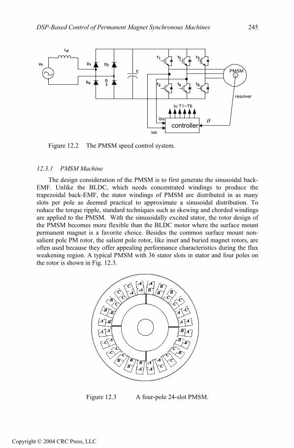
DSP-Based Control of Permanent Magnet Synchronous Machines 245
D1
D2D4
D3C
T1
T2
T3
T4
T5
T6
Ld
Vs
controller
to T1~T6
PMSM
ias
ibs θ
resolver
Figure 12.2 The PMSM speed control system.
12.3.1 PMSM Machine
The design consideration of the PMSM is to first generate the sinusoidal back-EMF. Unlike the BLDC, which needs concentrated windings to produce the trapezoidal back-EMF, the stator windings of PMSM are distributed in as many slots per pole as deemed practical to approximate a sinusoidal distribution. To reduce the torque ripple, standard techniques such as skewing and chorded windings are applied to the PMSM. With the sinusoidally excited stator, the rotor design of the PMSM becomes more flexible than the BLDC motor where the surface mount permanent magnet is a favorite choice. Besides the common surface mount non-salient pole PM rotor, the salient pole rotor, like inset and buried magnet rotors, are often used because they offer appealing performance characteristics during the flux weakening region. A typical PMSM with 36 stator slots in stator and four poles on the rotor is shown in Fig. 12.3.
Figure 12.3 A four-pole 24-slot PMSM.
Copyright © 2004 CRC Press, LLC

DSP-Based Control of Permanent Magnet Synchronous Machines 246
12.3.2 Power Electronic Converter
The PMSM shares the same topology of the power electronics converter as the BLDC motor drive system. The converter is the standard two-stage configuration with a dc link capacitor between a front-end rectifier and a three-phase full-bridge inverter as the output. The rectifier is either a full-bridge diode or power switch rectifier.
Due to the sinusoidal nature of the PMSM, control algorithms such as V/f and vector control, developed for other AC motors, can be directly applied to the PMSM control system. If the motor windings are Y-connected without a neutral connection, three phase currents can flow through the inverter at any moment. With respect to the inverter switches, three switches, one upper and two lower in three different legs conduct at any moment as shown in Fig. 12.4. PWM current control is still used to regulate the actual machine current. Either a hysteresis current controller, a PI controller with sine-triangle, or a SVPWM strategy is employed for this purpose. Unlike the BLDC motor, the three switches are switched at any time.
C
T2 T4 T6
ra Lc Ea
rb Lc Eb
rc Lc Ec
T1 T3 T5
Figure 12.4 The current path when the three phases are chopped.
12.3.3 Sensors
There are two types of sensors used in the PMSM drive system: the current sensor, which measures the phase currents, and the position sensor which is used to sense the rotor position and speed. The resistances in series with the power switches as shown in Fig. 12.2 are usually used as shunt resistor phase current sensors. Either an encoder or resolver serves as the position sensor. Rotor position is needed in order to synchronize the stator excitation of the PMSM with the rotor speed and position.
Figure 12.5 shows the structure of an optical encoder. It consists of a light source, slotted disk, and photo sensors. The disk rotates with the rotor. The two photo sensors output a logic “1” when they detect light. When the light is blocked, a logic “0” is generated by the sensors. When the light passes through the slots of
Copyright © 2004 CRC Press, LLC

DSP-Based Control of Permanent Magnet Synchronous Machines 247
the disk and strikes the sensor, a logic “1” is produced. These logic signals are shown in Fig. 12.5. By counting the number of pulses, the motor speed can be calculated. The direction of rotation can be determined by detecting the leading edge between signal A and signal B.
AB
Light
ω
Sensors A
B
Figure 12.5 The structure of encoder.
A resolver is a rotary electromechanical transformer. It outputs to sinusoidal signals such that one wave is a sinusoidal function of the rotor angle θ, while the other signal is a cosinusoidal function of θ. The difference between these two waveforms reveals the position of the rotor. Integrated circuits such as the AD2S80 can be used to decode the signals. The resolver output waveform and the corresponding rotor position are given in Fig. 12.6.
0 0.1 0.2 0.3 0.4 0.5 0.6 0.7 0.8 0.9 1-12
-10
-8
-6
-4
-2
0
2
4
6
8
10
12
sin(theta)
cos(theta)
Position
Figure 12.6 The resolver output and the corresponding rotor position.
Copyright © 2004 CRC Press, LLC

DSP-Based Control of Permanent Magnet Synchronous Machines 248
12.3.4 Controller
The LF2407 is used as the controller to implement speed control of the PMSM system. The interface of the LF2407 is illustrated in Fig. 12.7. Similar to the BLDC motor control system, three input channels are selected to read the two phase currents and resolver signal. Because a resolver is used in one case, the QEP inputs are not used. QEP inputs work only with a QEP signal that a rotary encoder supplies. The DSP output pins PWM1-PWM6 used to supply the gating signals to the switches and form the output of the control part of the system.
Gate Drive
ADCIN0
ADCIN1 PWM-1 & PWM-6
TMS320LF2407
ia
ib
ADCIN2 θ
Figure 12.7 The interface of LF2407.
12.4 Implementation of the PMSM System Using the LF2407
A block diagram of the PMSM drive system is displayed in Fig. 12.8. An assembly code algorithm was written for the LF2407 to implement the control system shown inside the dashed line in Fig. 12.8.
Copyright © 2004 CRC Press, LLC

DSP-Based Control of Permanent Magnet Synchronous Machines 249
Software+
refω
--
-
-∗
ecT
Vcs
Vbss
Sc
Sb
rω
SaVas
qsrvdsrv
*qsri
qsridsri
θ
ibs
ias
+
PWMInverter
d, q
a, b ,c PWMGenerator
PI
PI
d, q
a b,c
PMSM
+
PI0* =dsri
-
Speed
calculatorCurrent
calculator
Figure 12.8 Block diagram of PMSM speed control system.
The flowchart of the developed software is shown in Fig. 12.9. The control
program of the PMSM has one main routine and includes four modules:
1. Initialization procedure 2. DAC module 3. ADC module 4. Speed control module
The first three items introduced in Chapter 9. Hence, in the following section, only the speed control module is discussed in detail, with the corresponding assembly code given.
Copyright © 2004 CRC Press, LLC

DSP-Based Control of Permanent Magnet Synchronous Machines 250
No
Yes
Start
Initialization procedure
Read phase current ba ii , ; read the position signal;
Executespeed loop?
Set reference speed refω and calculate the actual speed
Speed PI regulator used to calculate the commend torque
Calculate the command q-axis current *qsi ; Set 0* =dsi
Current PI regulator used to calculate the qsds vv , in RRF
Transfer ba ii , to qsds ii , in Rotor Reference Frame (RRF)
Transfer qsds vv , in RRF to cba vvv ,,
Generate the PWM using sine-∆ generator
End
Output the program variables to DAC0~DAC3
Figure 12.9 The flow chart of PMSM control system.
Copyright © 2004 CRC Press, LLC

DSP-Based Control of Permanent Magnet Synchronous Machines 251
12.4.1 The Speed Control Algorithm
In the BLDC motor control system the Timer 1 underflow interrupt is used for the subroutine of speed control. This routine performs the tasks of:
• Reading the current and position signal, then generating the commanded speed profile.
• Calculating the actual motor speed, transferring the variables in the abc model to the d-q model and reverse.
• Regulating the motor speed and currents using the vector control strategy. • Generating the PWM signal based on the calculated motor phase voltages.
The PWM frequency is determined by the time interval of the interrupt, with the controlled phase voltages being recalculated every interrupt. The modules of this routine are detailed in the following section. The code below shows this routine. T1_PERIOD_ISR: ;Context save regs
MAR *,AR1 ;AR1 is stack pointer MAR *+ ;skip one position SST #1, *+ ;save ST1 SST #0, *+ ;save ST0 SACH *+ ;save acc high SACL * ;save acc low POINT_EV SPLK #0FFFFh,EVIFRA ;Clear all Group A interrupt ;flags (T1 ISR)
READ_SIG CALL ADC_CONV CALL CAL_TRIANGLE CALL ADC_DQ POINT_B0 LACC CL_SPD_FLG BCND CURRENT_CNTL,GT ;speed-loop?
; speed control SPEED_CNTL: POINT_B0
CALL SPEED_PROFILE CALL VTIMER_SEC CALL SPEED_CAL CALL D_PID_spd BLDD #D_PID_out ;iqsr SPLK #0, idsr_ref
; current control CURRENT_CNTL
CALL D_PID_cur BLDD #D_out_iq, Vqr BLDD #D_out_id, Vdr CALL DQ_ABC BLDD #a_out, Va BLDD #b_out, Vb BLDD #c_out, Vc
PWM_GEN CALL PWM_DRV DA_CONV CALL DAC_VIEW_Q15I ;Restore Context END_ISR:
MAR *, AR1 ;make stack pointer active
Copyright © 2004 CRC Press, LLC

DSP-Based Control of Permanent Magnet Synchronous Machines 252
LACL *- ;Restore Acc low ADDH *- ;Restore Acc high LST #0, *- ;load ST0 LST #1, *- ;load ST1 CLRC INTM RET
12.4.1.1 The Calculation of sinθ and cosθ
A lookup table is used to calculate the sine and cosine values of the rotor position θ. The rotor electrical angle depends only on its sine value in lookup table. The cosine value is calculated by shifting the sine value 90 degrees. The sine and cosine values, which are used in the transformation, can be obtained by simply knowing the rotor angle. The code below shows how to read the 1:1 look-up table with the LF2407. TRI_CAL
... LACC TRI_INT ;load accumulator AND #0ffh ;get lower bits ADD #SINTAB ;table read TBLR sine_a ... RET
The block of code below shows a portion of the sine value lookup table. ;SINVAL Index Angle Sin(Angle)
SINTAB .... .word 12539 ; 16 22.50 0.3827 .word 13279 ; 17 23.91 0.4052 .word 14010 ; 18 25.31 0.4276 .word 14732 ; 19 26.72 0.4496 .word 15446 ; 20 28.13 0.4714 .word 16151 ; 21 29.53 0.4929 .word 16846 ; 22 30.94 0.5141 .word 17530 ; 23 32.34 0.5350 .word 18204 ; 24 33.75 0.5556 .... RET
12.4.1.2 The abc-to-dq Transformation
The abc-to-dq transformation is defined in (12.9). It transfers the three-phase stationary motor model to a two-phase rotational motor model. In other words, under the restriction of the same motor performance, three phase stationary stator windings with 1200 separation can be replaced by a two-phase rotational winding with the q-phase 900 ahead of d-phase. The two-phase currents are related to the three-phase currents as defined by the transformation in (12.9). After this transformation, a significant simplification is achieved. The d and q-axis variables are decoupled and independent with time and rotor position, which implies that these variables become constant in steady state. It is possible to control the d and q
Copyright © 2004 CRC Press, LLC

DSP-Based Control of Permanent Magnet Synchronous Machines 253
variables independently. Since the d-axis variables are associated with the field variable and q-axis variables are related to the torque, this feature enables us to control the ac motor similar to a dc motor. For more detailed information on this topic we can refer to vector control theory. A portion of the abc-to-dq transformation using the assembly code is given in the code below: ABC_DQ:
...
... LACC #0 LT ABC_ain MPY sone_a LTA ABC_bin MPY sone_b LTA ABC_cin MPY sone_c LTA ABC_ain SACH ABC_D_out ... ... RET
12.4.1.3 The d-q to a-b-c Transformation
After the commanded d and q-axes variables are calculated, these two variables are transferred to the a-b-c stationary frame to drive the motor. This reverse transform is defined as follows:
(12.16) rqdrabcs fKf 0'=
where
++
−−=
21)
32sin()
32cos(
21)
32sin()
32cos(
21sincos
'
πθπθ
πθπθ
θθ
rr
rrr
r
rK (12.17)
An example of the assembly code to implement the above equation is given in the code below: DQ_ABC
...
... LACC #0 LT DQ_D_ref MPY sone_a LTa DQ_Q_ref MPY cosone_a MPYA cosone_b SACH DQ_aout ... ... RET
Copyright © 2004 CRC Press, LLC
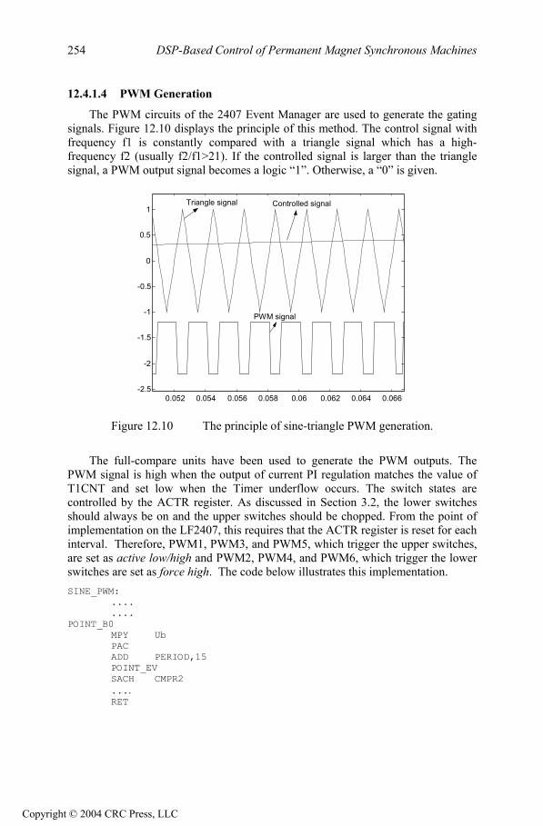
DSP-Based Control of Permanent Magnet Synchronous Machines
254
12.4.1.4 PWM Generation
The PWM circuits of the 2407 Event Manager are used to generate the gating signals. Figure 12.10 displays the principle of this method. The control signal with frequency f1 is constantly compared with a triangle signal which has a high-frequency f2 (usually f2/f1>21). If the controlled signal is larger than the triangle signal, a PWM output signal becomes a logic “1”. Otherwise, a “0” is given.
0.052 0.054 0.056 0.058 0.06 0.062 0.064 0.066-2.5
-2
-1.5
-1
-0.5
0
0.5
1 Triangle signal Controlled signal
PWM signal
Figure 12.10 The principle of sine-triangle PWM generation.
The full-compare units have been used to generate the PWM outputs. The
PWM signal is high when the output of current PI regulation matches the value of T1CNT and set low when the Timer underflow occurs. The switch states are controlled by the ACTR register. As discussed in Section 3.2, the lower switches should always be on and the upper switches should be chopped. From the point of implementation on the LF2407, this requires that the ACTR register is reset for each interval. Therefore, PWM1, PWM3, and PWM5, which trigger the upper switches, are set as active low/high and PWM2, PWM4, and PWM6, which trigger the lower switches are set as force high. The code below illustrates this implementation. SINE_PWM:
....
.... POINT_B0
MPY Ub PAC ADD PERIOD,15 POINT_EV SACH CMPR2 .... RET
Copyright © 2004 CRC Press, LLC

Chapter 13
DSP-BASED VECTOR CONTROL OF INDUCTION MOTORS
13.1 Introduction
For many years, induction motors have been preferred for a variety of industrialapplications because of their robust and rugged construction. Until a few years ago,the induction motor could either be plugged directly into the grid (uncontrolled) orcontrolled by means of the well-known scalar volts per Hertz (V/f) method. Invariable speed drives, both methods have serious drawbacks in the areas ofefficiency, reliability, and electromagnetic interference (EMI). With theuncontrolled method, even a simple change in the reference speed is not possible.Additionally, its system integration depends highly on the motor design (i.e.,starting torque vs. maximum torque, torque vs. inertia, number of pole pairs, etc).
The scalar V/f method is able to provide speed variation, but this methodcannot provide real-time control. In other words, the system response is only satisfactory at steady state and not during transient conditions. This results inexcessive current and over-heating, which necessitate the drive to be oversized.This over-design no longer makes the motor cost effective due to the high cost ofthe drive circuitry. By using real-time processors such as the LF2407 DSP controller, and with an accurate induction motor model, the development of highlyreliable and accurate variable speed motor drives becomes possible.
With the advent of field-oriented control (FOC) schemes, induction motors can be made to operate similar to separately excited dc motors. The indirect field oriented controls, or vector control, for speed and torque controlled AC drives arebecoming the industry standard in order to obtain high dynamic motor performance.
The control algorithm explained in this chapter is a rotor flux field-orientatedcontrol strategy. In this chapter, we will go through not only the implementation ofthe control software, but also the theoretical and practical aspects of the vector control. In the end, the reader will be familiar with the different parts of the FOC strategy of the induction motor as well as the developmental steps involved. Thereader should also be able to apply this induction motor drive solution to otherdesired systems. This chapter deals with the structure of an induction motor and develops its model followed by its FOC schemes. Finally, hardware and softwaredevelopment procedures covered.
13.2 Three-Phase Induction Motor Basic Theory
13.2.1 Three-Phase Induction Motor
Three-phase induction machines are asynchronous machines that operate belowthe synchronous speed when motoring and above the synchronous speed whengenerating. They are the most popular machine used in industry today and are
255
Copyright © 2004 CRC Press, LLC

DSP-Based Vector Control of Induction Motors256
rugged and require very little maintenance. Compared to dc motors, inductionmotors are not as easy to control. They typically draw large starting currents, aboutsix to eight times their full load values, and operate with lagging power factor whenloaded. However, with the advent of the vector control concept for motor control, itis possible to decouple the torque and the flux, thus making the control of theinduction motor very similar to that of the dc motor.
13.2.2 Induction Motor Construction
The dc motor can be called a conduction motor because the electric power isconducted directly to the armature through the brushes and commutator. In the caseof induction motors, the rotor receives power by induction; the same way asecondary of a two-winding transformer receives power from the primary. This is why the induction motor can be treated as a rotating transformer, where the primarywinding is stationary, but the secondary is free to rotate. We use this concept todevelop the equivalent circuit for induction motors.
The most popular type of induction motor used is the squirrel cage inductionmotor shown in Fig. 13.1. The rotor consists of a laminated core with parallel slotsfor carrying the rotor conductors, which are usually heavy bars of copper,aluminum, or alloys. One bar is placed in each slot; or rather, the bars are insertedfrom the end when the semi-closed slots are used. The rotor bars are brazed,electrically welded, or bolted to two heavy and stout short-circuiting end-rings, thuscompleting the squirrel cage construction. The rotor bars are permanently short-circuited on themselves. The rotor slots are usually not parallel to the shaft, but are given a slight angle, called a skew, which increases the rotor resistance due to increased length of rotor bars and an increase in the slip for a given torque. Theskew is also advantageous because it reduces the magnetic hum while the motor isoperating and reduces the locking tendency, or cogging, of the rotor teeth.
Figure 13.1 Short-circuited rotor bars of the squirrel cage induction motor.
Copyright © 2004 CRC Press, LLC

DSP-Based Vector Control of Induction Motors 257
13.2.3 Operation
When the three-phase stator windings are fed by a three-phase supply, a magnetic flux of a constant magnitude rotating at synchronous speed is createdinside the motor. Due to the relative speed between the rotating flux and thestationary conductors, an electromagnetic force (EMF) is induced in the rotor in accordance with Faraday’s laws of electromagnetic induction. The frequency of theinduced EMF is the same as the supply frequency, and the magnitude is proportional to the relative velocity between the flux and the conductors. Thedirection of this EMF is given by Fleming’s right-hand rule. Since the rotor barsform a closed path as shown in Fig. 13.1, a rotor current is produced which,according to Lenz’s law, is opposite to that of the relative velocity between therotating flux and the conductors. Therefore, the rotor current develops in the samedirection as the flux and tries to catch up with the rotating flux.
13.2.4 Slip
The difference between the synchronous speed e and the actual speed r ofthe motor is called the slip.
e
res (13.1)
13.3 Model of the Three-Phase Induction Motor in Simulink
13.3.1 Voltage Equations of the Idealized Motor Model
The idealized circuit model of the three-phase induction machine is shown inFig. 13.2:
r
r
as
bs cs
as
brar
cr
bscsar
br
cr
as axis
Figure 13.2 Idealized circuit model of the three-phase induction motor.
Copyright © 2004 CRC Press, LLC

DSP-Based Vector Control of Induction Motors258
Stator voltage equations:
t
asassas d
dirv (13.2)
t
bsbssbs d
dirv (13.3)
t
cscsscs d
dirv (13.4)
Rotor voltage equations:
t
arrarar d
driv ' (13.5)
t
brrbrbr d
driv ' (13.6)
t
crrcrcr d
driv ' (13.7)
Flux linkage equations:
(13.8)abcr
abcs
abcrr
abcrs
abcsr
abcss
abcr
abcs
i
i
LL
LL
where:
, , , i (13.9)
cs
bs
asabcs
cr
br
arabcr
cs
bs
asabcs
iii
i
cr
br
arabcr
iii
The stator-to-stator and rotor-to-rotor winding inductances are:
,
sslssmsm
smsslssm
smsmsslsabcss
LLLLLLLLLLLL
L
(13.10)
rrlrrmrm
rmrrlrrm
rmrmrrlrabcrr
LLLLLLLLLLLL
L
The stator-to-rotor mutual inductances are dependent on the rotor angle:
rrr
rrr
rrr
srTabc
rsabcsr LLL
cos)32cos()32cos()32cos(cos)32cos()32cos()32cos(cos
(13.11)
where:
Copyright © 2004 CRC Press, LLC

DSP-Based Vector Control of Induction Motors 259
= Stator winding leakage inductance per phasesL = Self inductance of stator windingssL = Peak value of stator to rotor mutual inductance smL
= Peak value of stator to rotor mutual inductance srLIf
Pg = air-gap permeance,then
, , ,gsss PNL 2grssr PNNL )3/2(2 CosPNL gssm
, (13.12))3/2(2 CosPNL grrm grrr PNL 2
We can see that the idealized machine is described by six first-order differentialequations; one for each winding. These differential equations are coupled to oneanother by the mutual inductances between the windings. The stator-to-rotor coupling terms are a function of the rotor position, so when the rotor rotates, thecoupling terms change with time. To solve this problem, induction motor equationsare transferred to the quadrature rotating reference frame such that the mutualinductances are not time dependent.
13.4 Reference Frame Theory
Reference frame theory is an integral part of electric drives. Reference framesare powerful tools for the analysis and application of sophisticated controltechniques, particularly in the case of the three-phase induction and synchronousmachines. Using reference frame theory, it is possible to transform the machinephase variables to another reference frame. By judicious choice of the referenceframes, it is possible to considerably reduce the complexity of the model machine.Reference frame theory has become especially important for digital motor controlwhere the need for accurate but simple motor models is essential. Though the theorycan be extended to any arbitrary reference frame, the two most commonly usedreference frames are the Stationary Reference Frame and the SynchronousReference Frame. The Clarke and Park transformations are used to transfer theinduction motor equations to these frames. The transformations are discussed in Chapter 10 in detail and are repeated here for reference. Clarke’s transformation is given by
(13.12)
cs
bs
as
ss
sds
sqs
fff
T
f
f
f
)0(
0
where
Copyright © 2004 CRC Press, LLC

DSP-Based Vector Control of Induction Motors260
2/12/12/12/32/302/12/11
3/2)0(T (13.13)
Park’s Transformation is represented by
(13.14)s
ds
sqs
eds
eqs
ff
f
fcossinsincos
where the rotor position is given by
(13.15)dte
13.5 Induction Motor Model in the Arbitrary q-d-0 Reference Frame
As mentioned previously, the two most common reference frames chosen torepresent the induction motor are the stationary and the synchronous referenceframes. The stationary reference frame has the q-d-0 variables of the machine in thesame frame as those normally used for the supply network. This choice of networkis usually made when the supply network is large or complex. In the case of thesynchronously rotating reference frame, the q-d-0 variables are constants at steadystate.
Assuming that the induction motor is rotating at speed in the direction ofrotor rotation, the machine equations in the stationary reference frame can be obtained by setting = 0. Likewise, the equations in the synchronous referenceframe are obtained by setting = e. Applying transformation to the stator windings a-b-c voltages, the stator winding q-d-0 voltages in the arbitrary referenceframe are obtained.
(13.16)sqds
sqd
sqd
sqd irpv 0000
000001010
where dtdp . Applying the transformation to the rotor voltage equation, we get
(13.17)rqdr
rqd
rqdr
rqd irpv 0000
000001010
)(
Stator and rotor flux linkage equations are given by
Copyright © 2004 CRC Press, LLC

DSP-Based Vector Control of Induction Motors 261
(13.18)
'0
'
'0
'
'
'
'0
'
'0
00000
0
00
0
00
000
0
0
00
000000
00
r
dr
qr
s
ds
qs
lr
mlr
m
mlr
m
m
ls
mls
mmls
r
dr
qr
s
ds
qs
i
i
iiii
LLL
L
LLL
LL
LLLLL
where the primed values are referred values to the stator side according to thefollowing relationships:
qrr
sqr N
N' (13.19)
drr
sdr N
N' (13.20)
qrr
sqr i
NNi ' (13.21)
drr
sdr i
NNi ' (13.22)
lrr
slr LNNL
2' (13.23)
Magnetizing inductance on the stator side is given by
rrr
ssr
r
sssm L
NN
LNN
LL23
23
23 (13.24)
The electromagnetic torque equation is given by
))(()(22
3 ''''drqrqrdrrdsqsqsds
rem iiiiPT
dsqrqsdrm
dsqsqsds
qrdrdrqr
iiiiLP
iiP
iiP
''
''''
223
223
223
(13.25)
13.6 Field Oriented Control
The term “vector” control refers to the control technique that controls both the amplitude and the phase of ac excitation voltage. Vector control therefore controlsthe spatial orientation of the electromagnetic fields in the machine. This has led to the coining of the term field oriented control (FOC), which is used for controllers
Copyright © 2004 CRC Press, LLC

DSP-Based Vector Control of Induction Motors262
that maintain a 90 spatial orientation between the critical field components. Theterm “field angle control” refers to the control strategy where the system is not at 90 of spatial orientation. In order to properly comprehend vector control, we mustunderstand the principle of dc machine torque control on which FOC is based.
13.7 DC Machine Torque Control
The required 90 of spatial orientation between key field components can be compared to the dc motor, where the armature winding magnetic field and the filed winding magnetic filed are always in quadrature. The objective is to force thecontrol of the induction machine to be similar to the control of a dc motor, i.e.,torque control. In dc machines, the field and the armature winding axes areorthogonal to one another, making the MMFs established orthogonal. If the ironsaturation is ignored, then the orthogonal fields can be considered to be completelydecoupled.
For dc machines, the developed torque is
(13.26)afaem IIKT )(where
= Constantak= Field flux)( fI
= Armature currentaISince the torque angle is always 90 , the flux and the torque can be controlled
independently. The torque is controlled by adjusting the field current If, and the fluxis directly controlled by adjusting the armature current Ia.
It is important to maintain a constant field flux for good torque control. It isalso important to maintain an independently controlled armature current in order toovercome the effects of the resistance of the armature winding, leakage inductance,and the induced voltage is needed. A spatial angle of 90 between the flux andMMF axes has to be maintained in order to limit interaction between the MMF andthe flux. If these conditions are met at every instant of time, the torque will always follow the current. In the case of dc machines, there is constant field flux and 90torque angle due to the commutator and the separate field excitation system. In ac machines, these conditions have to be attained by using external controls, makingthe system more complex and difficult to understand.
13.8 Field Oriented Control, Direct and Indirect Approaches
With vector control, the mechanically robust induction motors can be used in high performance applications where dc motors were previously used. The keyfeature of the control scheme is the orientation of the synchronously rotating q-d-0frame to the rotor flux vector. The d-axis component is aligned with the rotor flux
Copyright © 2004 CRC Press, LLC

DSP-Based Vector Control of Induction Motors 263
vector and regarded as the flux-producing current component. On the other hand,the q-axis current, which is perpendicular to the d-axis, is solely responsible fortorque production.
In order to apply a rotor flux field orientation condition, the rotor flux linkage is
aligned with the d-axis so and . By manipulating (13.16) and
(13.17) in the rotating reference frame,
0eqr r
edr ˆ
r , we can obtain the field orientedcondition.
mL
edre
dsistatesteadyedsimL
rLrre
drrLrre
drp 0 (13.27)
rr
eqsimLe
qs)irLmL
(r
rrslip ˆ (13.28)
eqsid
rLmLP
eT
eqsi
lrLmLmLe
qri
ˆ22
3(13.29)
We can find out that in this case i controls the rotor flux linkage and
controls the electromagnetic torque. The reference currents of the q-d-0 axis
are converted to the reference phase voltages (v as the
commanded voltages for the control loop. Given the position of the rotor flux andtwo-phase currents, this generic algorithm implements the instantaneous directtorque and flux control by means of coordinate transformations and PI regulators,thereby achieving accurate and efficient motor control.
eds
eqsi
e*qs(i )e*
ds,i )e*qs,ve*
ds
In asynchronous drives, the mechanical rotor angular speed is not, bydefinition, equal to the rotor flux angular speed. This implies that the necessaryrotor flux position cannot be detected directly by the mechanical position sensor provided with the asynchronous motor explained here.
It is clear that for implementing vector control we have to determine the rotorflux position. Two basic approaches to determine the rotor flux position angle have evolved. The direct scheme shown in Fig. 13.3(a), electrically determines the rotor flux position from measurements using field angle sensors. The indirect schemeillustrated in Fig. 13.3(b), measures the rotor position and utilizes the slip relation to compute the angle of the rotor flux relative to the rotor axis. From the feasibility point of view, implementation of the direct method is difficult if not sometimesimpossible. Therefore, in this chapter, the indirect method is considered as a solution for implementing FOC.
Copyright © 2004 CRC Press, LLC

DSP-Based Vector Control of Induction Motors264
FieldOriented
ControllerInverter
FluxCompensator
FS
IM
Te*
lqdr*
iabcs
FluxSensor
InductionMotor
lqdr
lqdm
(a) Direct flux sensing method.
FieldOriented
ControllerInverter
FluxCalculator
IM InductionMotor
PG SpeedSensor
w r
lqdr
Te*
lqdr*
iabcs
(b) Indirect flux sensing method.
Figure 13.3 Two generic types of induction motor vector control.
The indirect method is based on the calculation of the slip speed ,required for correct field orientation. Equations (13.27) and (13.28) show that wecan control torque and field by and i in the excitation frame. However, in the
implementation of field-oriented control, we need to know i and in the stationary reference frame. So, we have to know the angular position of the rotorflux to transform and i from the excitation frame to the stationary frame. By
using , which is shown in (13.28) and using actual rotor speed, the rotor flux position is obtained.
slip
dsi qs
ds qsi
dsi qs
slip
(13.30)(t)dtdt rt
ret
slip00
or
(13.31)(t)(t)dt rret
slip0
In literature, the algorithm of finding rotor flux position using the calculated and measured or is called the Current Model Method. The Current
Model takes and as inputs as well as the rotor mechanical speed and givesslip re
qsire
dsi
Copyright © 2004 CRC Press, LLC

DSP-Based Vector Control of Induction Motors 265
the rotor flux position as an output. Figure 13.4 shows the block diagram of the vector control strategy in which speed regulation is possible using a control loop.
The absence of the field angle sensors, along with the ease of operation at low speeds, has increased the popularity of the indirect vector control strategy. Whilethe direct method is inherently the most desirable scheme, it suffers from the unreliability in measuring the flux. Although the indirect method can approach the performance of the direct measurement scheme, its major weakness is the accuracy of the control gain, which heavily depends on the motor parameters.
FluxController
PI PI
PI
SVPWM
3-phaseInverter
Induction
motor
abc
CurrentModel
- i -
-
Vdc
ClarkeTransformation
ParkTransformation
Inv. ParkTransformation
r
+ +
+
Mechanical Speed of rotor
dse*
iqse* v qs
e*
v dse*
v qss*
v dss*
idss
iqss
idse
iqse
dqss
dqse
dq se
dqss
dqss
ref
rm
Figure 13.4 Vector control scheme for induction motor.
As shown in Fig. 13.4, two-phase current feeds the Clarke transformationblock. These projection outputs are indicated as i and . These twocomponents of the current provide the inputs to Park’s transformation, which givesthe currents in the excitation reference frame. The and i components,which are outputs of the Park transformation block, are compared to their referencevalues , the flux reference, and , the torque reference. The torque command,
, comes from the output of the speed controller. The flux command, i , is theoutput of the flux controller which indicates the right rotor flux command for everyspeed reference. For i we can use the fact that the magnetizing current is usuallybetween 40 and 60% of the nominal current. For operating in speeds above thenominal speed, a field weakening section should be used in the flux controller
sds
i
sqsi
eqs
eqds
e*ds
eds
e*dsi e*
qsie*qsi e*
ds
Copyright © 2004 CRC Press, LLC

DSP-Based Vector Control of Induction Motors266
section. The current regulator outputs, and , are applied to the inverse Park
transformation. The outputs of this projection are and v , which are the
components of the stator voltage vector in the orthogonal reference frame.They form the inputs of the SVPWM block. The outputs of this block are the signalsthat drive the inverter.
e*dsv e*
qsv
dqs
sds
sdsv
s
sqs
Note that both the Park and the inverse Park transformations require the exactrotor flux position, which is given by the current model block. This block needs therotor resistance or rotor time constant as a parameter. Accurate knowledge of therotor resistance is essential to achieve the highest possible efficiency from thecontrol structure. Lack of this knowledge results in the detuning of the FOC. InFig. 13.4, a SVPWM has been used to emulate v and in order to implementcurrent regulation. The reader can find more information about SVPWM in Chapter11.
sqsv
13.9 Simulation Results for the Induction Motor Control System
The drive system with the proposed control strategy has been simulated prior tolaboratory experimentation. For simulation purposes, software packages such asMatlab/SimulinkTM and Advanced Continuous Simulation Language (ACSL)TM can be used. In this section, SimulinkTM has been used to model the induction motor,the vector control, and the SVPWM. The induction motor has been simulated with the dynamic q-d-0 model using the nominal parameters as given in Table 13.1. Thedc link voltage in the simulation is equal to 100V. Maximum phase current hasbeen limited to the rated value. Initially, the magnetizing current is set at 60% of the rated current. The simulation results of the control system to a command speed areshown in Fig. 13.5.
13.10 Induction Motor Speed Control System
Based on the previous analysis, an induction motor speed control system is developed as shown in Fig. 13.6. The total control system consists of the inductionmotor, the power electronics converter, the sensor, and the controller. Thesecomponents are discussed in detail in the following section.
Copyright © 2004 CRC Press, LLC

DSP-Based Vector Control of Induction Motors 267
0 1 2-150
0
150
(a)
0 1 2-150
0
150
(b)
0 1 2-5
5
15
(c)
0 1 2-20
0
20
(d)
0 1 240
50
60
(e)
0 1 2-5
5
15
(f)
0 1 2-75
0
75
(g)
Time (sec.)
Figure 13.5 (a) reference speed, (b) actual speed, (c) load torque, (d)electromagnetic torque, (e) stator d-axis current in the rotating reference frame, (f)
stator q-axis current in the rotating reference frame, (g) phase-A current.
Controller
D1
D2D4
D3C
T1
T2
T3
T4
T5
T6
Vs
to T1~T6
IM
ias
ibs
Encoder
QEP-A
QEP-B
Figure 13.6 Induction motor speed control system.
Copyright © 2004 CRC Press, LLC

DSP-Based Vector Control of Induction Motors268
13.11 System Components
13.11.1 Power Electronic Converter
As shown in Fig. 13.9, the power electronics converter in induction motorcontrol system consists of two parts: a front-end rectifier and a three-phase full-bridge inverter in the right-hand side. The rectifier usually is a full-bridge diode. Incase of a regenerative system, a power switch rectifier is used.
The inverter is usually responsible for both the electronic commutation andcurrent regulation. Pulse-width-modulated current controllers are typically used toregulate the actual machine currents to match the sinusoidal current referencewaveforms.
The power hardware used to implement and test the induction motor drivesystem can support an input voltage of 1200 V and a maximum current of 50 A. Thehardware is based on six power IGBTs (SKM 50GB 123D), driven by the DSP controller via the integrated driver SKHI22. The power and the control componentsare insolated from one another by the use of opto-couplers in the gate drive signalpath.
Table 13.1 Induction motor parameters
Motor Parameters ValueRated power 3.0 hpRated Voltage 230/460 VoltRated Current 7.6/3.8 AmpRated Speed 1760 rpmPole pairs 2Rated frequency 60 Hz Nominal efficiency 87.5%Base impedance 23.64631Stator resistance 0.044225Magnetizing impedance 1.1178Stator leakage impedance 0.05956Rotor leakage impedance 0.05956Rotor resistance 0.03078
13.11.2 Sensors
Two types of sensors for the induction motor control system are used. One is acurrent sensor and the other is a position sensor. The phase current sensing is performed via two current sensors supplied with 15 V. Their maximum inputcurrents can be changed by the number of turns in the primary winding, and theoutput is a bipolar voltage.
Copyright © 2004 CRC Press, LLC

DSP-Based Vector Control of Induction Motors 269
Encoders or resolvers serve as the position sensor because every point of therotor position is needed to synchronize the rotor with the stator excitation. Figure13.7 shows the structure of an optical encoder. It consists of a light source, aradially slotted disk and photoelectric sensors. The disk rotates with the rotor. The two photo sensors detect the light passing through the slots in the disk. When the light is hidden, a logic “0” is generated by the sensors. When the light passesthrough the slots of the disk, a logic “1” is produced. These logic signals are shown in Fig. 13.7. By counting the number of pulses, the motor speed can be calculated.The direction of rotation can be determined by detecting the leading signal between signal A and signal B.
AB
LightSensors A
B
Figure 13.7 The structure of an encoder.
13.11.3 Controller
The controller of the induction motor control system is used to read thefeedback current and position signals, to implement the speed or torque control algorithm, and to generate the gate signals based on the control signal. Analogcontrollers or digital signal processors can perform this task. We have used theLF2407 as a controller.
The interface of the LF2407 is illustrated in Fig. 13.8. Two quadraturecounters detect the rising and falling edges of the encoder signals. Two inputchannels related to the 10-bit Analog-to-Digital Converter (ADC) are selected to read the two-phase currents. The pins PWM1 to PWM6 output the gating signals tothe gate drive circuitry.
Copyright © 2004 CRC Press, LLC

DSP-Based Vector Control of Induction Motors270
Q EP-1
Q EP-2
PW M -1 & PW M -6G ateD rive
T M S320F2407
En A
AD CIN -1
AD CIN -0Ia
Ib
En B
Figure 13.8 The interface of LF2407.
13.12 Implementation of Field-Oriented Speed Control of Induction Motor
Some practical aspects of implementing the block diagram of Fig. 13.8 arediscussed in this section and subsections. The software organization, the utilizationof different variables, and the handling of the DSP controller resources aredescribed. In addition, the control structure for the per-unit model is presented.Next, some numerical considerations have been made in order to address theproblems inherent within fixed-point calculation. As described, current model is one of the most important blocks in the block diagram depicted in Fig. 13.4. Theinputs of this block are the currents and mechanical speed of rotor. Two sections ofthis chapter deal with technical points that should be considered during current andspeed measurement, as well as their scaling. Also, there are some points to be notedduring development of the current model in software; therefore, one section isdedicated to current model implementation. A PI controller is used in the field-oriented speed control of the induction motor as a regulator for current and speedcontrol. The PI structure and block diagram are presented in another section.
13.12.1 Software Organization
The body of the software consists of two main modules: the initialization module and the PWM Interrupt Service Routine (ISR) module. The initialization model is executed only once at startup. The PWM ISR module interrupts the waiting infinite loop when the timer underflows. When the underflow interrupt flagis set, the corresponding ISR is served. Figure 13.9 shows the general structure ofthe software. The complete FOC algorithm is executed within the PWM ISR so thatit runs at the same frequency as the switching frequency or at a fraction of it. The wait loop could be easily replaced with a user interface [1].
Copyright © 2004 CRC Press, LLC

DSP-Based Vector Control of Induction Motors 271
HardwareInitialization
Start
VariableInitialization
Inf. Loop PWMI.S.R
Figure 13.9 General structure of software.
13.12.2 Base Values and Per-Unit Model
It is often convenient to express machine parameters and variables of per-unitquantities. Moreover, the LF2407 is a fixed point DSP, so using a normalized per-unit model of the induction motor is easier than using real parameters. In thismodel, all quantities refer to the base values. Base power and base voltage are selected, and all parameters and variables are normalized using these basequantities. Although one might violate this convention from time to time when dealing with instantaneous quantities, the rms values of the rated phase voltage and current are generally selected as the base voltage for the a-b-c variables while the peak value is generally selected as the base voltage for d-q variables. The basevalues are determined from the nominal values by using (13.31), where , V ,are the nominal phase current, the nominal phase to neutral voltage, and the nominalfrequency in a star-connected induction motor, respectively. The base valuedefinitions are as follows:
nI n nf
b
bb
nb
nb
nb
VfVV
II
22
2
(13.31)
bI and V are the maximum values of the nominal phase current and voltage,is the electrical nominal rotor flux speed, and is the base flux.
b b
b
Copyright © 2004 CRC Press, LLC

DSP-Based Vector Control of Induction Motors272
13.12.3 Numerical Considerations
The per-unit model has been developed so that the software representation of speed, current, and flux is equal to 1.0 when the motor has reached its nominalspeed under nominal load and magnetizing current. During transients, the currentmight reach higher values than the nominal current in order to achieve a short response time. Also, the motor speed might exceed the nominal speed ( ), and then every per-unit value might be greater than 1.0. This fact necessitates foreseeingthese situations and determines the most suitable numerical format used for thesoftware.
bI
b
13.12.4 The Numerical Format Determination
The numerical format used in the major part of this chapter is as follows: four bits are dedicated to the integer part, and twelve bits are dedicated to the fractionalpart. This numeric format is denoted by Q4.12. The resolution for this format isgiven by
00024414.02112
With the sign extension mode of the LF2407 set, the link between the real quantity and its Q4.12 format representation is illustrated in Fig. 13.10.
24.4e-5
32767
-32767
-8
7.99975586
Figure 13.10 Representation of Q4.12 format.
The reason for this particular format is that the drive control quantities are, for the most part, not usually greater than four times their nominal values. In otherwords, not greater than four when the per-unit model is considered. Where this is not the case, a different format will be chosen. The selection of a range of [-8,8]ensures that the software values can handle each drive control quantity, not onlyduring steady state operation but also during transient operation.
Copyright © 2004 CRC Press, LLC

DSP-Based Vector Control of Induction Motors 273
The Qx.y numeric format uses x bits for the integer part and y bits for thefractional part, so the resolution is . If z is the per-unit value to implement, then its software value is
y2yz 2 in Qx.y format. Care must be taken when performing
operations with a generic Qx.y format. Adding two Qx.y formatted numbers mayresult in numerical representation overflow. To avoid this kind of problem, one possible solution is to perform the addition in the high side of the Accumulator and set the saturation bit. Another option is to assume that the result will not be out of the maximum range.
The second solution can be used in this implementation if we know that the control quantities do not exceed half of the maximum value in the Q4.12 format.The result can still be represented in the Q4.12 format and directly considered as Q4.12 format, thereby allowing for a higher level of precision. As far as themultiplication is concerned, the result (in the 32-bit Accumulator) must either beshifted x positions to the left and the least significant word stored or be shifted ypositions to the right with the last significant word being stored. The stored result is in Qx.y format. Figure 13.11 shows two Qx.y formatted 16-bit variables that aremultiplied by one another.
The result of this multiplication in Qx.y format is represented in gray in the 32-bit Accumulator. Both solutions are depicted in Fig. 13.11.
yx
yx
MSB LSB MSB LSB
yx
*
yx
yx
High Word Low Word
1
2
Figure 13.11 (1) Left shift and store high accumulator, (2) Right shift and store
low accumulator.
Note that in this section there are also constants that cannot be represented bythe Q4.12 format. Operations requiring different formats follow exactly the sameprocess as that explained above.
Copyright © 2004 CRC Press, LLC

DSP-Based Vector Control of Induction Motors274
13.12.5 Current Measurement
The field-oriented control structure requires two-phase current as inputs. Here,current transducers sense these two currents. The current sensor output therefore needs to be rearranged and scaled so that it may be used by the control software inQ4.12 format value. The complete process of acquiring the current is depicted inFig. 13.12.
SignalConditioner A/D
10-bitRange
adjustmentor offset
CurrentGain
Iabc 1023:0
512:
-512
i abc
Figure 13.12 Current measurement block diagram.
The output signal of current transducer can be either positive or negative. This signal must be adjusted by the analog interface into a range of (0,3.3V) to allow the ADC module to read both positive and negative values. Figure 13.13 shows theinside of the signal conditioner.
CT
1.65v offset
To A/D1.65v
:-1.65v
Iabc
Figure 13.13 Current signal conditioner block diagram.
The amplifier gain is chosen such that sensing maxIIabc results in theabsolute value of the amplifier output to be equal to 1.65V. Note thatrepresents the maximum measurable current, which is not necessarily equal to themaximum phase current. This information is useful at the point where currentscaling becomes necessary. The ADC input voltage is now converted into a 10-bitdigital value. The 1.65V analog offset is digitally subtracted from the convertedresult, thereby giving a signed integer value of the sensed current. The result of thisprocess is shown in Fig. 13.14.
maxI
Copyright © 2004 CRC Press, LLC

DSP-Based Vector Control of Induction Motors 275
512
-512
i
max
max
-i SensedCurrent
Prescaled Value
Figure 13.14 Sensed current values before scaling.
Because the variable format is Q4.12, the sensed phase currents must now beexpressed with the per-unit model and then be converted into the Q4.12 format.Notice that the per-unit representation of the current is defined as the ratio betweenthe measured current and the base current, and the maximum current handled by thehardware is represented by the value 512. The per-unit current conversion into theQ4.12 format is achieved by multiplying the sensed current by the followingconstant:
max
5124096
II
Kb
cu (13.32)
In one single calculation, this constant performs not only the per-unit modelingbut also the numerical conversion into Q4.12 format. When nominal current flowsin a motor running at nominal speed, the current sensing and scaling block output is 1000h (equivalent to 1 per-unit).
The reader may change the numerical format by amending the numerator valueand may adapt this constant to its own current sensing range by recalculatingwith its own value. In this control system, maximum measurable current andbase current are = 12A and = 10.7A, respectively. The constant value is:
cuK
maxIImax bI
Q8.8808978
12710512
4096 hF..
Kcu
Note that is outside the Q4.12 format range. The most appropriate formatto accommodate this constant is the Q8.8 format, which has a resolution of
cuK
Copyright © 2004 CRC Press, LLC

DSP-Based Vector Control of Induction Motors276
00390625.0218
and the following correspondence to Fig. 13.15.
39.06e-4
32767
-32767
-128
127.996
Figure 13.15 Representation of Q8.8 format.
The currents of two phases can be sampled by means of the DSP controllerusing two channels of the ADC module. The block of assembly code below readsand scales the current of phase A.
; Reading and scaling current value of phase A LDP #RESULT2>>7LACL RESULT2 ;Reading A/D result register RPT #5 ;Shift to right 6 times SFRAND #0000001111111111bSUB #512 ;Subtracting offset value LDP #IA SACL IA LAR AR0, #KcurLT IA MPY * ;Multiplying by coefficient to scale the ;current valuePACSFLSACH IA,7 ;Save current value in proper variable
13.12.6 Speed Measurement
As previously mentioned, for finding rotor flux position, it is necessary tomeasure the rotor mechanical speed. Usually an incremental encoder is used as aspeed sensor. A 64 pulse per revolution incremental encoder is used to measure themotor speed. The software speed resolution is thus based onincrements per revolution. This sensor has two outputs and produces two pulsetrains that are 90
256644
0 out of phase with respect to each other. The periods of the pulses
Copyright © 2004 CRC Press, LLC

DSP-Based Vector Control of Induction Motors 277
proportionally to the rotor speed. The two output channels A and B of speed sensorcan be wired directly to the QEP input pins of the LF2407.
Because a low count encoder is used in the control system, and because thisencoder does not have enough resolution at low speeds, the control system uses twomethods in order to estimate the induction motor speed. One method has enoughaccuracy in the high speed region, above 200 rpm, and the other has appropriateresolution in the low speed region under 200 rpm. The first method, which is utilized during high speed, is based on counting the number of encoder pulses in a specific time interval. However, the second method is based on the measurement of time between two encoder pulses. Based on the motor speed, the developed programcan utilize the advantages of both methods and switch between the two methodsbased on the actual speed of the motor.
13.12.7 Speed Estimation during High-Speed Region
As previously mentioned, this method is based on counting the number of encoder pulses in a specified time interval. The QEP assigned timer counts the number of pulses and records it in the timer counter register (TxCNT). As themechanical time constant is much slower than the electrical one, the speed regulation loop frequency might be lower than the current loop frequency. Thespeed regulation loop frequency is obtained in this program by means of a softwarecounter. This counter accepts the PWM interrupt as input clock and its period is thesoftware variable called SPEEDSTEP. The counter variable is named speedstep.When speedstep is equal to SPEEDSTEP, the number of pulses counted is stored inanother variable called and thus the speed can be calculated. The schemedepicted in Fig. 13.16 shows the structure of the speed feedback generator.
pn
CounterQEP
speedstep is equal to SPEEDSTEP?
K
w m
speed
No
yes
Do nothing
FromEncoder
Figure 13.16 Block diagram of speed feedback calculator.
Assuming that is the number of encoder pulses in one SPEEDSTEP period
when the rotor turns at the nominal speed, a software constant should bechosen as follows:
pn
speedK
pspeed .nKh01000
Copyright © 2004 CRC Press, LLC

DSP-Based Vector Control of Induction Motors278
The speed feedback can then be transformed into a Q4.12 format, which can beused in the control software. In the proposed control system, the nominal speed is 1800 rpm and SPEEDSTEP is set to 125. can be calculated as follows: pn
28860
4641800pp TSPEEDSTEPn (13.33)
where 41033
pwmp f
T (PWM frequency is 10 kHz but the program is
running at 3333 Hz) and hence is given by:speedK
883802214288
4096 .QhE.Kspeed
Note that is out of the Q4.12 format range. The most appropriate format to handle this constant is the Q8.8 format. The speed feedback in Q4.12 format is then obtained from the encoder by multiplying by . The flowchart of speed measurement is presented in Fig. 13.17. A portion of the assemblycode that measures and scales the rotor speed is given below.
speedK
pn speedK
; Start of speed calculation in high speed region LDP #T2CON>>7 LACC T2CNT ;Read counter register of encoder pulse ;counter SPLK #7FFFh, T2CNT ;Set counter value to 7FFFh SUB #7FFFh ;Subtract 7FFFh from counter read value ;to omit ;offsetLDP #Speedtmp ;Save this value in Speedtmp SACL Speedtmp LAR AR0, #KspeedLT Speedtmp ;Multiply Speedtmp by Kspeed to find out ;scaled speed valueMPY *PACSACH N,4 ;Save speed value in proper variable in ;Q4.12 format
Copyright © 2004 CRC Press, LLC

DSP-Based Vector Control of Induction Motors 279
w = Kspeed*np
speedstep = speedstep-1
speedstep = 0
speedstep = SPEEDSTEP
np = TxCNT
Yes
No
TxCNT=0
Figure 13.17 Complete flowchart of speed measurement block during high-
speed region.
13.12.8 Speed Measurement during Low-Speed Region
To detect the edges of two successive encoder pulses, the developed programcan use either the QEP counter or the capture unit input pins. The program has tomeasure the time between two successive pulses, so therefore it must utilize anotherGP timer. In this program, Timer 3 has been dedicated to the time measurement.During the interrupt service routine of the capture unit or counter QEP, speed can becalculated. To obtain the actual speed of the motor, the appropriate number isdivided by the value in the count register of Timer 3.
As it can be inferred, at very low speeds an overflow may occur in Timer 3.The counter would then reset itself to zero and start counting up again. This eventresults in a large error in speed measurement. To avoid this event, Timer 3 will be disabled in the overflow interrupt service routine. However, this timer is enabled in the capture unit (counter QEP) interrupt.
The prescalar of Timer 3 is set to x/128, giving the input clock a 234375 Hzfrequency. To obtain the speed value in Q4.12 format, 431238 (a constantnumber) is loaded in the accumulator. This number will be divided by the counter
Copyright © 2004 CRC Press, LLC

DSP-Based Vector Control of Induction Motors280
register of Timer 3. The flow-chart of this implementation is presented in Fig.13.18.
Temp=T3CNT
T3CNT=0
ACC=31238*32
w=np/8
Enable Timer3
np=ACC / Temp
Start of Capture unit orCounter QEP ISR
End of Capture unit orCounter QEP ISR
T3CNT=FFFFh
Timer 3Disable
Start of Timer 3Overflow ISR
End of Timer 3Overflow ISR
Figure 13.18 Flowchart of speed measurement at low speed.
13.12.9 The Current Model
In indirect FOC, the Current Model is used to find the rotor flux position. This module takes and i as inputs plus the rotor electrical speed and thencalculates the rotor flux position. The current model is based on (13.27) and (13.28). Equation (13.27) can be written as follows, in transient case:
dsi qs
dsm
drdr
mr
r iLdt
dLr
L (13.34)
Assume mm
dr iL
where i is the magnetizing current, therefore (13.34) can be
written as follows:
m
dsmmr iiidtdT (13.35)
In order to find the rotor flux speed, we use (13.36) which has been inferredfrom (13.28) and (13.30) in a per-unit system.
bmr
qsre
bs iT
idtdf 1 (13.36)
Copyright © 2004 CRC Press, LLC

DSP-Based Vector Control of Induction Motors 281
where is the rotor flux position and r
rr r
LT and re are the rotor time constant
and rotor electrical speed, respectively. The rotor time constant is critical to the correct functionality of the Current Model. This system outputs the rotor flux speed, which in turn will be integrated to get the rotor flux position. Assuming that
, (13.35) and (13.36) can be discretized as follows: )()1( kk qsqs ii
)1(
)()1()1(
)()()()1(
1
k
kKk
kkkk
mr
qs
brs
mrdsr
pmrmr
i
i
Tnf
iiTT
ii
(13.37)
For example, let the constants r
p
TT
and brT
1 be renamed to and ,
respectively. Here ,
tK rK
mHLr 8.73 73.0rr , and Hzfn 60 . So for and we have:
tK
rK
12.400610237.2637710232.30
11
12.400010967.21009.1013/10000
33
33
1
QBhT
K
QChTT
K
brt
r
pr
By knowing the rotor flux speed ( ), the rotor flux position (sf cm ) is computed bythe integration formula in the per-unit system.
Tfkkk sbcmcm ..
)()()1( (13.38)
As the rotor flux position range is [0, 2 ], 16-bit integer values have been usedto achieve the maximum resolution. Figure 13.19 illustrates the relationshipbetween the flux position and its numerical representation:
65535
9.58e-5
(rad)
Figure 13.19 Relation between rotor flux position and its numerical
representation.
Copyright © 2004 CRC Press, LLC

DSP-Based Vector Control of Induction Motors282
In (13.38), let Tfsb be called inc . This variable is the rotor angle variationwithin one sampling period. At nominal operation (in other words when , the
mechanical speed is 1800 rpm),
1sf
inc is equal to rad11309.03/10000
602 . In one
mechanical revolution performed at nominal speed, there are 56.0 11309
2
increments of the rotor flux position. Let K be defined as the constant, whichconverts the [0, 2 ] range into the [0, 65535] range. K is calculated as follows:
15.10492117056
65536 QhK
Note that here we choose the Q1.15 format for this constant because the maximum value of which is 65535, represents 1 per-unit and the value of cannot be greater than 1 per-unit ( 2 ). With the help of this constant, the rotor fluxposition computation and its formatting becomes:
)()()1( kkk scmcm Kf
Thus, the Current Model is a block, as depicted in Fig. 13.20, with three input variables , ,dsi dsi re (represented in Q4.12 format) and one output, which is therotor flux position cm represented as a 16-bit integer value. The code block belowshows a portion of the assembly algorithm that determines the rotor flux position.
CurrentModel
Ids
Iqs
re
cm
Figure 13.20 Inputs and output of the Current Model block.
;start of calculation rotor flux position LDP #IDS_R ;start of calculation magnetizing ;current LACC IDS_R SUB Imr SACL temp1 MAR *, AR0 LAR AR0, #Kr LT temp1 MPY * PACSACH temp1,4 LACC temp1 ADD Imr SACL Imr
Copyright © 2004 CRC Press, LLC

DSP-Based Vector Control of Induction Motors 283
BCND Imr_Neqz, NEQ LACC #0 SACL temp1 B IQS_Rp
Imr_Neqz: ;if Imr != 0 then start of slip ;frequency calculation
LACC Imr SACL temp2 LACC IQS_R ABSSACL temp1LACC temp1,12 RPT #15 SUBC temp2 SACL temp1 LACC IQS_R BCND IQS_Rp, GT ;if IQS is negative then change sign of ;IQS/Imr LACC temp1 NEGSACL temp1
IQS_Rp:
LAR AR0, #Kt LT temp1 MPY * PACSACH temp1,4 LACC temp1 ADD N ;add rotor speed to slip frequency SACL fs ;find rotor flux speed
;end of calculation of rotating flux speed ;Start of finding Rotor Flux position by using integral of fs
LACC fs ABSSACL temp1 LAR AR0, #Kfs ;multiplying fs bu Kfs, a constant value
;to find increment or decrement in rotor ;flux positionLT temp1 MPY * PACSACH teta_inc,4bit fs,0 BCND fs_neg, TC ;go to fs_neg if teta_inc is negative LACL teta_inc ADDS TETA SACL TETA ;find new rotor flux position if ;teta_inc is negativeB fs_pos
fs_negLACL TETA SUBS teta_inc SACL TETA ;find new roto flux position if teta_inc ;is positive
fs_pos; end of finding Rotor flux position
13.12.10 The PI regulator
An electrical drive based on the Field Orientated Control needs two constants as control parameters: the torque component reference and the flux component*e
qsi
Copyright © 2004 CRC Press, LLC

DSP-Based Vector Control of Induction Motors284
reference . The classical PI regulator is well suited to regulate the torque and flux feedback to the desired values. This is because it is able to reach constant references by correctly setting both the proportional term ( ) and the integral
term ( ), which are, respectively, responsible for the error sensibility and for thesteady state error. The numerical expression of the PI regulator is as follows:
*edsi
)(kY
pK
iK
(13.39)1
0)()()(
k
nnkikp eeKeK
which is represented in Fig. 13.21.
Kp
Ki
1/Z
Uref
Ufbk
ek
xi
Yk
Figure 13.21 Classical PI regulator structure in discrete domain.
The limiting point is that during normal operation, large reference valuevariations or disturbances may occur, resulting in the saturation and overflow of theregulator variables and output. If they are not controlled, this non-linearitydetriments the dynamic performance of the system. To solve this problem, onesolution is to add to the previous structure a correction of the integral component asdepicted in Fig. 13.22 [2].
Kp
Ki
1/Z
Uref
Ufbk
ek
xi
Yk Y1k
Kcor
-
+
Figure 13.22 Numerical PI regulator with correction of the integral term.
The PI regulators are implemented with output saturation and integralcomponent correction. The constants Kpi, Ki, Kcor, proportional, integral, andintegral correction components, are selected based on the sampling period and onthe motor parameters. These values should be changed based on the motor speed.These changes can be done automatically within a dummy loop in the program. To
Copyright © 2004 CRC Press, LLC

DSP-Based Vector Control of Induction Motors 285
show the routine of the PI controller in assembly, the following section of code isgiven:
LDP #N_ref ;Start of PI procedure LACC N_ref ;Load reference speed SUB N ;subtract motor speed from reference
;speed to find errorSACL err_N ;put error in err_N LACC xi_N,12 ;load previous value of PI output ;controller LAR AR0, #Kp_N ;start of multiplication Kp*errorLT err_N MPY * APAC ;Add previous output of controller with ;new value Y(p)=Y(p-1)+Kp*errorSACH Upi_N,4 LACC Upi_N ;start of positive saturation value < ;(max) ABSSUB IQS_Rmax BCND N_sat, GT ;if value is less than (max) go to ;negative saturationLACL Upi_N B N_LIMIT
N_satBIT Upi_N, 0 ;start of negative saturation (min)< ;value BCND Upi_Ngz, NTC ;if Upi_N is positive, then go to ;Upi_Ngz LACL IQS_Rmin SACL Upi_N BN_LIMIT
Upi_NgzLACL IQS_Rmax SACL Upi_N
N_LIMITSACL IQS_R ;start of correction procedure LAR AR0, #Ki_N LT err_N MPY * PACADD xi_N, 12 SACH xi_N,4LACC xi_N ;start of saturation on integrator ;output ABSSUB IQS_Rmax BCND x_sat, GT LACL xi_N B x_LIMIT
x_satBIT xi_N, 0 BCND xi_Ngz, NTC ;if xi_N is positive, then go to xi_Ngz LACL IQS_Rmin SACL xi_N B x_LIMIT
xi_NgzLACL IQS_Rmax SACL xi_N
x_LIMITSACL xi_N
; end of PI procedure
Copyright © 2004 CRC Press, LLC

DSP-Based Vector Control of Induction Motors286
13.12.11 Calculation of Sine and Cosine Functions
In order to generate the sine and the cosine of an angle, a sine table and indirectaddressing mode by auxiliary register AR has been used. This algorithm and code examples are presented in Chapter 11. The flow chart of the field-oriented speedcontrol of induction motor is presented in Fig. 13.23. This routine is placed insidethe PWM interrupt service routine.
Reading Ia and Ib
Iabc Idqs
Clark Trans.
Regulatespeed?
Calculate speed
Start of PWM ISR
s
Speed PI regulator,Calculate Iqs
s*
High speed?
Idqs Idqs
Current Model
Ids and Iqs
to PI regulator and calculate Vds and Vqs
(Vdqs) (Vdqs)New .r
SV PWM
end of PWM ISR
s e
ee
e e
e s
Calculate SIN and COS of qr
Yes
No
Yes
No
Figure 13.23 Flow chart of FOC software.
Copyright © 2004 CRC Press, LLC
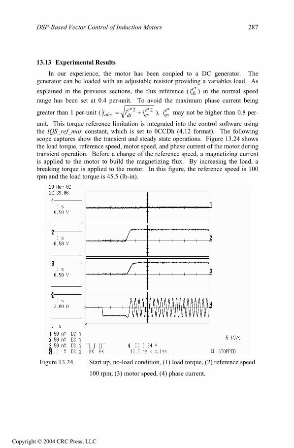
DSP-Based Vector Control of Induction Motors 287
13.13 Experimental Results
In our experience, the motor has been coupled to a DC generator. Thegenerator can be loaded with an adjustable resistor providing a variables load. As explained in the previous sections, the flux reference ( i ) in the normal speedrange has been set at 0.4 per-unit. To avoid the maximum phase current being
greater than 1 per-unit (
*eds
2*2* eqs
edsabc iii ), may not be higher than 0.8 per-
unit. This torque reference limitation is integrated into the control software using the IQS_ref_max constant, which is set to 0CCDh (4.12 format). The followingscope captures show the transient and steady state operations. Figure 13.24 showsthe load torque, reference speed, motor speed, and phase current of the motor duringtransient operation. Before a change of the reference speed, a magnetizing currentis applied to the motor to build the magnetizing flux. By increasing the load, a breaking torque is applied to the motor. In this figure, the reference speed is 100rpm and the load torque is 45.5 (lb-in).
*eqsi
Figure 13.24 Start up, no-load condition, (1) load torque, (2) reference speed
100 rpm, (3) motor speed, (4) phase current.
Copyright © 2004 CRC Press, LLC

DSP-Based Vector Control of Induction Motors 288
13.14 Conclusion
In this chapter, the theory of field-oriented control of induction motors was described. The structure and organization of software written for the LF2407 DSP controller was also presented. Some technical points and tools were presented to assist in developing a working model for an induction motor drive. The modular structure of this presentation and guidelines allow the reader to quickly grasp the aspects of FOC, thereby assisting the reader in developing software for specific needs.
References
1. Texas Instruments, Implementation of a Speed Field Orientated Control of Three Phase AC Induction Motor using TMS320LF240, Literature Number: BPRA076, March 1998.
2. Texas Instruments, Field Orientated Control of Three Phase AC-motors, Literature Number: BPRA073, December 1997.
Copyright © 2004 CRC Press, LLC

Chapter 14
DSP-BASED CONTROL OF SWITCHED RELUCTANCE MOTOR
DRIVES
14.1 Introduction
Switched Reluctance Motor (SRM) drives are relatively new entities in the perpetually growing market of Adjustable Speed Motor Drives (ASMD). A rugged, modular structure and a relatively simple geometry are among the advantages of the SRM drive. In addition, the absence of magnetic sources, i.e., windings or permanent magnets on the rotor shown in Fig. 14.1, makes SRM relatively easy to cool and insensitive to high temperatures. The latter is of prime interest in applications that demand operation under harsh conditions such as automotive starter or alternator.
Figure 14.1 Rotor and stator of an 8/6 SRM.
As a singly excited synchronous machine, SRM generates its electromagnetic torque solely on the principle of reluctance. In most electric machines, an attraction and repletion force between the magnetic fields caused by the armature and field windings forms the dominant part of the torque. In a SRM, the tendency of a polarized rotor pole to align with an excited stator pole is the only source of torque. It must be noted that optimal performance is achieved by proper positioning of the current pulse with respect to the magnetic status of the machine. Therefore, the sensing of the rotor position becomes an integral part of the control in a SRM drive.
A unipolar power inverter is usually used to supply the SRM. The generation of the targeted current profile is performed using a hysteresis or PWM type current controller. Although a square-shaped current pulse is commonly used for excitation in a SRM, different optimal current profiles are sometimes used to mitigate the undesirable effects of excessive torque undulation and audible noise. In fact, SRM drives serve as an outstanding example of advanced motor drive systems where the focus is not on the complicated geometries of the motor, but on the development of a sophisticated control algorithm. The development of complex control algorithms
289
Copyright © 2004 CRC Press, LLC

DSP-Based Control of Switched Reluctance Motor Drives
290
is facilitated by the recent development of high-performance, cost-effective DSP-based controllers.
Optimal torque control is the major differentiating factor among various arts of electric drives. A detailed explanation of the torque generation process and optimal torque control in the four quadrants of operation of a SRM is given. Later, the development of speed controllers will be discussed.
14.2 Fundamentals of Operation
Switched reluctance machines can operate as either a motor or a generator. To explain the torque generation process, we investigate the mechanism of electromechanical energy conversion. As shown in Fig. 14.2, in order to establish a reluctance torque, a stator phase is excited at unaligned position displayed by a in the figure, viz., the position at which a pair of stator and rotor poles exhibits its largest air gap length. By magnetizing the stator pole, the closest rotor pole will be magnetically polarized and will experience an attractive force. The tangential component of this force substantiates an electromagnetic torque in the direction which reduces the air gap length. The shape of the current is usually controlled such that a maximum torque per ampere is generated. As the rotor approaches the aligned position, shown by u in the figure, the radial component of the attraction force becomes dominant and the tangential component reduces to zero. Therefore, it makes economic sense to remove the current before the aligned position. The shaded area in Fig. 14.2 depicts the magnetic energy converted into mechanical form, whereas the area denoted by “R” demonstrates the magnetic energy that has not been converted into useful work. Notably, the ratio between mechanical work and total converted energy into magnetic form is an indication of power quality in SRM drives. In Fig. 14.2, ψ and θ represent the flux linkages and rotor position, respectively.
Figure 14.2 Electromechanical energy conversion in SRM.
Copyright © 2004 CRC Press, LLC

DSP-Based Control of Switched Reluctance Motor Drives 291
In order to obtain motoring action, a stator phase is excited when the rotor is moving from the unaligned position toward the aligned position. Similarly, by exciting a stator phase when the rotor is moving from aligned toward unaligned position, a generating action will be achieved. By sequential excitation of the stator phases, a continuous rotation can be achieved. Figure 14.3 shows the distribution of the magnetic field during commutations in an 8/6 SRM drive. Notably, the direction of the rotation is opposite that of the stator excitation. A short flux path in the back-iron of the motor occurs in each electrical cycle. This, in turn, may cause asymmetry in the torque production process.
Figure 14.3 Illustration of short vs. long flux paths for a 8/6 SRM.
Proper synchronization of the stator excitation with the rotor position is a key step in the development of an optimal control strategy in SRM drives. Because the magnetic characteristics of the SRM, such as phase inductance or phase flux linkage, portray a one-to-one correspondence with the rotor position, they may be directly used for control purposes. In either case, direct or indirect detection of the rotor position forms an integral part of the control in the SRM drives.
Copyright © 2004 CRC Press, LLC

DSP-Based Control of Switched Reluctance Motor Drives
292
The asymmetric bridge shown in Fig. 14.4 is the most commonly used power electronics inverter for a SRM drive. This topology features a unipolar architecture that allows for satisfactory operation in SRM drives. If both switches are closed, the available dc link voltage is applied to the winding. By opening the switches, the negative dc link voltage will be applied to the winding and freewheeling diodes guarantee a continuous current in the windings. Obviously, by keeping one of the switches closed while the other one is open, the respective freewheeling diode will provide a short-circuited path for the current. This topology can be used effectively to implement PWM-based or hysteresis-based current regulation as demanded by the control system. However, one should notice that at high speeds the induced EMF in the winding is dominant and does not allow effective control of the current waveform. Therefore, current regulation is an issue related only to the low speed mode of operation. During generation, the mechanical energy supplied by the prime mover will be converted into an electrical form manifested by the induced EMF. Unlike the motoring mode of operation, this voltage acts as a voltage source that increases the current in the stator phase, thereby resulting in the generation of electricity.
Figure 14.4 An asymmetric bridge with the front end rectifier for a 3-φ SRM drive.
14.3 Fundamentals of Control in SRM Drives The control of electromagnetic torque is the main differentiating factor between
various types of adjustable speed motor drives. In switched reluctance motor drives, tuning the commutation instant and profile of the phase current controls electromagnetic torque. Figure 14.5 depicts the basics of commutation in SRM drives. It can be seen that by properly positioning the current pulse, one can obtain positive (motoring) or negative (generating) modes of operation.
The induced EMF and electromagnetic torque generated by the SRM drive can be expressed in terms of co-energy as follows:
ωθθω
θi
ddL
iWE c )(2
≈∂∂
∂=
2)(21 i
ddLWT cθθ
θ≈
∂∂
= (14.1)
Copyright © 2004 CRC Press, LLC

DSP-Based Control of Switched Reluctance Motor Drives 293
where iLWc ,,, θ , and ω stand for co-energy, phase inductance, rotor position, phase current, and angular speed, respectively.
It must be noted that the nonlinear effects of magnetic saturation are neglected here. It is evident that a positive torque is achieved only if the current pulse is positioned in a region with an increasing inductance profile. Similarly, a generating mode of operation is achieved when the excitation is positioned in a region with a decreasing inductance profile. In order to enhance the productivity of the SRM drive, the commutation instants, (i.e., onθ , ) need to be tuned as a function of the angular speed and phase current. To fulfill this goal, the optimization of torque per Ampere is a meaningful objective. Therefore, exciting the motor phase when the inductance has a flat shape should be avoided. At the same time, the phase current needs to be removed well before the aligned position to avoid the generation of negative torque.
offθ
Figure 14.5 Commutation in SRM drives.
14.4 Open Loop Control Strategy for Torque
By the proper selection of the control variables, commutation instants, and reference current, an open loop control strategy for SRM drive can be designed. The open loop control strategy is comprised of the following steps:
• Detection of the initial rotor position. • Computation of the commutation thresholds in accordance with the sign of
torque, current level, and speed.
Copyright © 2004 CRC Press, LLC

DSP-Based Control of Switched Reluctance Motor Drives
294
• Monitoring of the rotor position and selection of the active phases. • A control strategy for regulation of the phase current at low speeds.
Each step is explained in detail in the subsequent sections.
14.4.1 Detection of the Initial Rotor Position
The main task at rotor standstill is to detect the most proper phase for initial excitation. Once this is established, according to the direction of rotation, a sequence of stator phase excitation will be put in place. The major difficulty in using commercially available encoders is that they do not provide a position reference. Therefore, the easiest way to find rotor position for motor startup is to align one of the stator phases with the rotor. This can be achieved by exciting an arbitrary stator phase with an adequate current for a short period of time. Once the rotor is in an aligned position, a reference initial position can then be established. This method requires an initial movement by the rotor, which may not be acceptable in some applications. In these cases, the incorporation of a sensorless scheme at standstill is sought out. Although the explanation of sensorless control strategies for rotor position detection is beyond the extent of this chapter, due to its critical role, the detection of rotor position at standstill is explained here.
To detect rotor position at standstill, a series of voltage pulses with fixed and sufficiently short duration are applied to all phases. By consequent comparison between the magnitudes of the resulting peak currents, the most appropriate phase for conduction is selected. Figure 14.6 shows a set of normalized inductance profiles for a 12/8 SRM drive.
Figure 14.6 Assignment of various regions according to inductances in a 12/8
SRM drive.
Copyright © 2004 CRC Press, LLC

DSP-Based Control of Switched Reluctance Motor Drives 295
A full electrical period is divided into six separate regions according to the magnitudes of the inductances. Due to the absence of the induced voltage and small amplitude of currents, one can prove that the following relationship will hold for the magnitudes of measured currents:
ABC
BusABC L
TVI ∆= (14.2)
where ∆T, VBus, and LABC stand for duration of pulses, dc link voltage, and phase inductances, respectively. Table I summarizes the detection process for a 12/8 SRM drive. Once the range of position is detected, the proper phase for starting can be easily determined. Furthermore, in each region there exists a phase that offers a linear inductance characteristic. This phase can be used for the computation of rotor position using (14.2).
Table I Detection of best phase to excite at standstill
Region Condition Rotor angle [mech]
I CBA III << 0* 5.70 << θ
II CAB III << 0*0 155.7 << θ
III ACB III << 0*0 5.2215 <<θ
IV ABC III << 0*0 305.22 <<θ
V BAC III << 0*0 5.3730 <<θ
VI BCA III << 0*0 455.37 <<θ
The flowchart shown in Fig. 14.7 summarizes the detection process at standstill.
Figure 14.7 Detection of rotor position at standstill.
Copyright © 2004 CRC Press, LLC

DSP-Based Control of Switched Reluctance Motor Drives
296
14.4.2 Computation of the Commutation Thresholds
In the next step, the commutation angles for each phase should be computed and stored in memory. If the commutation angles are fixed, computing the thresholds is relatively straightforward. It must be noted that within each electrical cycle, every phase should be excited only once. In addition, in a symmetric machine, phases are shifted by
s
rsNNN 0360)( −
=∆θ (14.3)
where and stand for the number of rotor and stator poles. Given a reference for rotor position such as the aligned rotor position with phase-A, one can compute and store the commutation instants for each phase. The commutation thresholds are usually converted into a proper scale so they can be compared with the value of a counter which tracks the number of incoming pulses from the position sensor. If a particular encoder can generate N pulses per mechanical revolution, then every mechanical degree corresponds to
sN rN
360.4 N pulses received by the QEP
counter of the LF2407. The quadrature input of the LF2407 is designed for commercially available encoders with quadrature output. Notably, this component can increase the resolution of the sensed position by a factor of four.
If optimal performance of the machine is targeted, the effects of rotational speed and current must be taken into account. Figure 14.8 shows a typical current pulse for SRM drive. To achieve optimal control, the delay angles during the turn-on and turn-off process need to be taken into account. By neglecting the effects of motional back-EMF in the neighborhood of commutation, which is a valid assumption as turn-on and turn-off instants occur close to unaligned and aligned position, respectively, one can calculate the delay angles as
−
=−max
lnrIVV
rLu
delayonωθ
≈ −−
u
adelayondelayoff L
IL maxθθ (14.4)
where VLL au ,,, ω , and r denote unaligned inductance, aligned inductance, angular speed, bus voltage, and stator phase resistance, respectively. The dependency of the aligned position inductance upon maximum phase current is an indication of the nonlinear effects of saturation that need to be taken into account. As the speed and level of current increases, one needs to adopt the commutation angles using (14.4). As can be seen, the dependency of commutation angle upon the angular speed is linear while its dependency upon the maximum phase current has a very nonlinear relationship.
Copyright © 2004 CRC Press, LLC

DSP-Based Control of Switched Reluctance Motor Drives 297
14.4.3 Monitoring of the Rotor Position and Selection of the Active Phases
Once the previous steps are done, one can start with the main control tasks, namely, enforcing the conduction band and regulating the current. The block diagram depicted in Fig. 14.9 shows the structure used in a typical algorithm, which forms the basic control strategy of the SRM drive. Monitoring the rotor position is a relatively easy task with a LF2407. By properly initializing the second timer in the event manager, it can be programmed to act as a counter for QEP encoder input. The content of this counter can be accessed at any stage of the program. This makes the monitoring of the rotor position an easy task. For the first task in the interrupt service routine, the current value of the rotor position will be compared against the commutation thresholds, and phases that should be on will be identified. In the next step, the current in active phases where an active phase is referred to as a phase that is turned on will be regulated.
14.4.4 A Control Strategy for Regulation of the Phase Current at Low Speeds
At low speeds where the induced EMF is small, a method for control of the phase current is necessary. In the absence of such routines, the phase current will increase exponentially, possibly damaging the semiconductor devices or motor windings. Hysteresis and PWM control strategies are commonly used for regulating the phase current at low speeds. At higher speeds, the presence of a significantly larger back-EMF limits the growth of the phase current and there is no need for such regulation schemes. The profile of the regulated current depends on the control objective. In most applications, a flat-topped or square shaped current pulse will be used. Figure 14.10 shows a regulated current waveform along with the gate pulse that is recorded at low speed region.
Figure 14.8 A typical current pulse at low speeds.
Copyright © 2004 CRC Press, LLC

DSP-Based Control of Switched Reluctance Motor Drives
298
Figure 14.9 Block diagram of the basic control in SRM drives
Figure 14.10 Phase current waveform and the gating signal without optimization Reference current = 5.5 A; conduction angle = 180°(electrical)
(operating speed = 980 RPM; output power = 120 W)
Copyright © 2004 CRC Press, LLC
DSP-Based Control of Switched Reluctance Motor Drives 299
In order to conduct hysteresis control, the currents in active phases need to be sensed. Once the phase current is sampled, it needs to be converted into digital form. This can be done using the on-chip analog-to-digital converter of the LF2407. The control rules for a classic two switch per phase inverter shown in Fig. 14.4 are given by:
• If , then both switches are on. This results in applying the bus voltage across the coil terminals.
II ≥min
• If , then both switches are turned off. This results in applying the negative bus voltage across the coil terminals.
II ≤max
• If , there is no need to make any changes in the status of the switches (i.e., if the switches are on they remain on and if they are off they remain off).
maxmin III ≤≤
By simple comparison between the sampled current and current limits, one can develop a hysteresis control strategy. Since the current is sampled during each interrupt service routine, the time period of the interrupt should be sufficiently small to allow for a tight regulation. Because in most practical cases only two phases conduct simultaneously, and given the speed of 30 MIPS (millions of instructions per seconds) in LF2407 (or 40MIPS for LF2407A) the interrupt service time should be very small.
PWM technique can also be used in control of the phase current in SRM drive. The LF2407 offers a fully controllable set of PWM signals via the Compare Units. The frequency and duty cycle of these PWM pulses can be adjusted at any stage of the program by the setting of two peripheral registers. This valuable feature can easily accommodate the control needs of a three-phase SRM drive system. In the case of a four-phase SRM drive, the fourth PWM signal can be generated by using one of the timer compare outputs. The block diagram depicted in Fig. 14.11 shows a typical PWM regulator as used for the control of the phase current in a SRM drive. It must be noted that due to the variable time constant of the stator windings, a fixed set of gains in the controller will not be sufficient, and a gain scheduling technique should be added. One practical way to achieve this is to obtain the gains corresponding to the aligned and unaligned rotor time constants, and then use a linear interpolation method to find the controller gains at the intermediate positions.
Copyright © 2004 CRC Press, LLC

DSP-Based Control of Switched Reluctance Motor Drives
300
Figure 14.11 Block diagram of the PWM current control in SRM drive.
The block diagram in Fig. 14.12 summarizes the various steps along with the
peripherals used in the LF2407. The main inputs to the program consist of commutation angles and the current profile. The quadrature outputs of an encoder have been used to determine the rotor position and angular speed of the drive. The phase currents have been sampled and converted into digital form to be used in current control. The output gates have been chosen from the general purpose input/output (GPIO) pins. The interface, conditioning circuit, and buffers are not shown in this picture. The control routine, used for the detection of active phases and hysteresis/PWM control of the phase currents, is combined in the software to form the final gating signal.
Figure 14.12 Block diagram of the basic control in SRM drive system.
Copyright © 2004 CRC Press, LLC

DSP-Based Control of Switched Reluctance Motor Drives 301
Once the basic operation of the SRM drive is established, one can design and develop closed loop forms of the control. In the following sections, closed loop torque and speed control routines in the SRM drive are discussed, including four-quadrant operation of the drive.
14.5 Closed Loop Torque Control of the SRM Drive
As SRM technology begins to emerge in the form of a viable candidate for industrial applications, the significance of reliable operation under closed-loop torque, speed, and position control increases. Figure 14.13 depicts a typical cascaded control configuration for SRM drives. The main control block is responsible for generating the gate signals for the power switches. It also performs current regulation and phase commutation functions. In order to perform these tasks, it requires reference current, commutation instants, and a sequence of excitation. The torque controller provides the reference current, while the information regarding the commutation is obtained from a separate block that coordinates motoring, generating, and direction of rotation, as demanded by the various types of control. The various feedback information is generated using either estimators or transducers.
Figure 14.13 Cascaded control configuration for a SRM drive system.
Depending on the application, an adjustable speed motor drive may operate in various quadrants of the torque/speed plane. For instance, in a water pump application, where control of the output pressure is targeted, torque control in one quadrant is sufficient, whereas in an integrated starter/alternator, four-quadrant operation is necessary. Figure 14.14 shows the minimum requirement of an adjustable speed motor drive for performing torque, speed, and position control tasks. A speed controller may issue positive (motoring) or negative (generating) torque commands to regulate the speed. In a similar way, a position controller will ask for positive (clockwise) and negative (counter clockwise) speed commands. The accommodation of such commands will span all four quadrants of operation in the
Copyright © 2004 CRC Press, LLC

DSP-Based Control of Switched Reluctance Motor Drives
302
torque/speed plane. As a result, four-quadrant operation is a necessity for many applications in which positioning the rotor is an objective. In order to achieve four-quadrant operation in SRM drives, the direction of rotation in the air gap field needs to be altered. In addition, to generate negative torque during generation mode, the conduction band of the phase should be located in a region with negative inductance slope.
Figure 14.15 depicts a general block diagram of the closed loop torque control system. The main modules in this figure are:
• An estimator for the average/instantaneous electromagnetic torque. • A feed-forward function for fast and convergent tracking of the
commanded torque. • A computational block to determine commutation instants according to the
sign of demanded torque and magnitude of the phase current.
Figure 14.14 Minimum requirement of an adjustable speed drive for performing
torque, speed, and position control.
The estimator for average/instantaneous electromagnetic torque is designed based on (14.1). The design also incorporates an analytical model of the phase inductance/flux linkage as shown below:
( ) ( ) ( ) ( ) )2(cos)(cos, 210 θθθ rr NiLNiLiLiL ++= (14.5) where L0, L1, and L2 represent polynomials, that reflect the nonlinear effects of saturation. Moreover, the inverse mapping of the torque estimator is used to form a feed-forward function. In the absence of the torque sensor/estimator, this feed-forward function can be used effectively to perform open loop control of the torque. The use of a feed-forward controller accelerates the convergence of the overall torque tracking. The partial mismatch between reference and estimated torque is then compensated via a PI controller. It must be noted that the introduction of the measured torque into the control system requires an additional analog-to-digital conversion. Figure 14.16 shows a comparison between the estimated and measured torque in a 12/8 SRM drive at steady state when responding to a periodic ramp function in closed loop control. The average torque estimator shows good accuracy. The existence of a 0.4 Nm averaging error is due to the fact that iron and stray
Copyright © 2004 CRC Press, LLC

DSP-Based Control of Switched Reluctance Motor Drives 303
losses are not included in the torque estimator. In order to perform this test, a permanent magnet drive acting as an active load was set in a speed control loop running in the same direction at 800 rpm.
As mentioned earlier, operation in all four quadrants of the torque vs. speed plane is a requirement for many applications. Given the symmetric shape of the inductance profile with respect to the aligned rotor position, one can expect that for a given conduction band at a constant speed, current waveforms during motoring and generating should be a mirror image of each other. However, one should note that the back-EMF during generation acts as a voltage source resulting in an increase of phase current even after a phase is shut down. This may cause some complications in terms of stability at high speeds. In order to alter the direction of rotation, the only necessary step is to change the sequence of excitation. Notably the sequence of excitation among stator phases is opposite of the direction of rotation. The transition between two modes needs to be quick and smooth. Upon the receipt of a command requesting a change in direction, the excited phase needs to be turned off to avoid generating additional torque. Regenerative braking should be performed simultaneously. This requires the detection of a phase in which the inductance profile has a negative slope. The operation in generation mode continues until the speed decays to zero or a tolerable near zero speed. At this time, all the phases will be cleared and a new sequence of excitation can be implemented. Speed reversal during generating is not a usual case because the direction of rotation is dictated by the prime mover. In the case that the speed reversal is initiated by the prime mover, the SRM controller needs to be notified. Otherwise, a mechanism for the detection of rotation direction should be in place. Such a mechanism would detect any unexpected change of mode, i.e., motoring to generating.
Figure 14.15 General block diagram of the torque control system.
Copyright © 2004 CRC Press, LLC

DSP-Based Control of Switched Reluctance Motor Drives
304
00.5
11.5
22.5
33.5
44.5
0 5 10 15 20 25
time[sec]
Torq
ue[N
-m]
(a) Estimated average torque.
-1
0
1
2
3
4
5
6
0 5 10 15 20 25
time[sec]
Torq
ue[N
-m]
(b) Measured torque.
Figure 14.16 Comparison between measured and estimated torque.
14.6 Closed Loop Speed Control of the SRM Drive
As it is the next step in developing a high performance SRM drive, speed control is explained. As shown in Fig. 14.17, a cascaded type of control can be used to perform closed loop speed control. The speed can be sensed using the position information that is already provided by the encoder. Because the SRM is a synchronous machine, one may choose the electrical frequency of excitation for control purposes. The relationship between mechanical and electrical speeds is given by
mre N ωω = (14.6) where is the number of rotor poles. Ultimately, success in performing tightly regulated speed control depends upon the performance of the inner torque control system as depicted in Fig. 14.17. It is recommended that a feed-forward function be used to mitigate the initial transients in issuing commands to the torque control system.
rN
Copyright © 2004 CRC Press, LLC

DSP-Based Control of Switched Reluctance Motor Drives 305
Figure 14.17 Closed loop speed control of SRM drive.
14.7 Summary
SRM drives are making their entry into the adjustable speed motor drive market. To take full advantage of their capacities, the development of high-performance control strategies has turned into a necessity. The advent of cost-effective DSP-based controllers provides an opportunity to engineer for this need in an effective way. A successful implementation of these methodologies demands a good understanding of the torque generation process. Basic control methods for the SRM drive have been discussed. These include the principles of design for closed loop control strategies. More advanced technologies, such as position sensorless and adaptive control, are also being investigated by many researchers across the globe, and there have been great advances in these areas as well. It is expected that developments in better efficiency, fault tolerance, and compactness will come about as a result of these efforts in years to come.
14.8 Algorithm for Running the SRM Drive using an Optical Encoder
A simple algorithm for running a four-phase SRM drive using a LF2407 DSP controller is shown in this section. One may change t-on and t-off to adjust the commutation angles. In order to adjust the current magnitude, HLIMIT and LLIMIT should be tuned. A level-three interrupt has been used to perform the control of the conduction band and phase current in an encoder-based architecture. By aligning one phase, a reference for rotor position is provided. Next, the commutation instants for each phase have been computed and the interrupt routine has been invoked. Because there is no control on the current during the aligning process, a current limiting algorithm is required. To obtain a better understanding of the algorithm, the following flow chart is prepared
Copyright © 2004 CRC Press, LLC

DSP-Based Control of Switched Reluctance Motor Drives
306
Figure 14.18 Flow chart of the overall SRM drive.
Copyright © 2004 CRC Press, LLC

Chapter 15
DSP-BASED CONTROL OF MATRIX CONVERTERS
15.1 Introduction
Traditionally, ac voltages and currents having variable amplitude and frequency are generated in PWM modulated voltage-source inverters (PWM-VSI). These inverters need dc power, which is usually supplied by a diode bridge rectifier or a PWM active rectifier. This can be considered indirect power conversion because the topology is based on two types of power conversions via a dc link (capacitor). Indirect power converters perform the ac/ac power conversion by converting ac to dc through a rectifier, and then converting dc back to ac via an inverter. This operation is illustrated in Fig. 15.1.
DCAC Input Utility
Energy Storage
Output Load ACDC
(a) indirect power conversion
ACInput Utility
Output Load AC
(b) direct power conversion
Figure 15.1 Two power conversion schemes.
An alternative to indirect power converters is the direct power converter such as a cycloconverter or a forced-commutated cycloconverter (FCC). Since both of these converters perform true direct ac/ac power conversion, they need no intermediate power converting process. Cycloconverters, using thyristors, are typically utilized for power applications in the megawatt-range. However, the inability of the thyristors to control turn off limits the output frequency to half the input frequency.
The FCC, otherwise known as a matrix converter, has no limit on output frequency due to the fact that it uses semiconductor switches with controlled turn-off capability. Examples of these semiconductor switches include the IGBT, MOSFET, and MCT. Since being introduced in 1976, the matrix converter has received an increased amount of interest because it lacks the dc link and posses the capability of bi-directional power flow control. The matrix converter has been studied intensely as an alternative to indirect power converter systems.
307
Copyright © 2004 CRC Press, LLC

DSP-Based Control of Matrix Converters
308
15.2 Topology and Characteristics
The matrix converter is a single-stage converter, and has an array of m by n bi-directional switches which directly connect an m-phase voltage source to an n-phase load. The number of input phases must be at least three, and the number of output phases can be chosen from one to theoretically infinity. Figure 15.2 shows a schematic representation of the most plausible application in which a matrix converter connects a three-phase voltage source to a three-phase load. The matrix converter is characterized by its ability to connect any input phase, a, b, or c to any output phase A, B, or C at any instant. This allows bi-directional power flow and sinusoidal input currents by directly interconnecting the input and output voltage system via bi-directional switches. The advantages and disadvantages of the matrix converter, when compared with conventional indirect power conversion, can be listed as follows:
A. Advantages
• No dc link capacitor or inductor • Sinusoidal input and output currents • Possible power factor control • Four-quadrant operation • Compact and simple design • Regeneration capability
B. Disadvantages
• Reduced maximum voltage transfer ratio (0.866) • Many bi-directional switches needed • Increased complexity of control • Sensitivity to input voltage disturbances • Complex commutation method
Although the matrix converter has several disadvantages, these drawbacks have been mostly overcome. For example, the reduced voltage transfer ratio problem has been worked around by designing motors that reach maximum flux at the reduced matrix converter output voltage. The problem of physical space needed by the increased number of switches has been overcome by the development of power electronic building blocks such as the Eupec ECONOMACTM matrix module, or by modifying the matrix converter topologies to use a fewer number of switches. The complexity of control and sensitivity to input voltage disturbances has also been solved by the development of different control algorithms. In all, the progress of the matrix converter has significantly improved its performance, rendering it an acceptable choice for compact and integrated converter-motor drives.
Because the matrix converter is fed by an input voltage source and connected to an inductive load, the following two basic rules must be always followed.
Copyright © 2004 CRC Press, LLC

DSP-Based Control of Matrix Converters 309
• Any two input phase voltages must not be connected to the same output line to avoid a short-circuit condition.
• Any output phase cannot be opened to avoid the interruption of inductive loads.
By defining the switching functions of each bidirectional switch as
where,
=openS
closedSts
ij
ijij ,0
,1)( CBAjcba ,,,,,i ∈∈ (15.1)
the above two constraints can be expressed by
CBAjsss cjbjaj ,,,1 ∈=++ (15.2) With these constraints, the 3 by 3 matrix converter can allow only 27 possible
switching states among the possible 512 switching combinations.
Va
IMVb
Vc
ia
ib
ic
LF
CF
iA
iB
iC
VAB
VBC
A
B
C
a
b
c
SaA
SbA
ScA
SaB
SbB
ScB
SaC
SbC
ScC
Bi-directional Switch
Motor
Input Filter
Matrix Converter Figure 15.2 The three-phase matrix converter topology.
15.3 Control Algorithms
Two control schemes, the Venturini method and the space vector modulation method (SVM), provide independent control of the magnitude and the frequency of the output voltages.
Copyright © 2004 CRC Press, LLC

DSP-Based Control of Matrix Converters
310
15.3.1 Venturini Method
In 1980, Venturini and Alesina proposed a PWM modulation method for the matrix converter, known to as the “Venturini method”. The Venturini method can be summarized as follows: for a given set of three-phase input voltages, a desired set of three-phase output voltages can be synthesized by sequential piecewise sampling of the input waveforms. The duration of each sample is derived mathematically to ensure that the average value of the actual output waveform within each sampling cycle tracks the required output waveforms. This method is also used to control the three-phase input currents.
If the input and output voltage vectors are defined by
=
=
)()()(
,)()()(
tVtVtV
VtVtVtV
V
C
B
A
out
c
b
a
in (15.3)
the relationship between them can be written as
inout VMV ⋅=
=
)()()(
)()()()()()()()()(
)()()(
333231
232221
131211
tVtVtV
M
tmtmtmtmtmtmtmtmtm
tVtVtV
c
b
a
C
B
A
44444 34444 21
(15.4)
where M is the instantaneous transfer function matrix. From the input-output power balance (Pin=Pout), the following relationships are valid for the input and output currents:
outT
in iM ⋅=i
3214444 34444 21321
out
C
B
A
Tin
c
b
a
i
tititi
M
tmtmtmtmtmtmtmtmtm
i
tititi
=
)()()(
)()()()()()()()()(
)()()(
332313
322212
312111 (15.5)
where T
M is the transpose of matrix M .
Each entity of the instantaneous transfer function matrix, mij(t) (i,j=1,2,3), represents the duty cycle function of a bi-directional switch within one switching period. The duty cycle functions are limited by the existence constraint
)3,2,1,(1)(0 =≤≤ jitmij (15.6) and the restriction imposed on the matrix converter switches by (15.2)
∑m (15.7) )3,2,1(1)(3
1==
=it
jij
Copyright © 2004 CRC Press, LLC

DSP-Based Control of Matrix Converters 311
The maximum voltage transfer ratio of input to output voltage was limited by 0.5 in the initial approach of the Venturini method. Later, this method was further modified in order to increase the maximum voltage transfer ratio to 0.866.
15.3.2 The Initial Approach
We first find the transfer function matrix M , which consists of the duty cycle functions of the nine bi-directional switches. For a set of three-phase input supply voltages
(15.8)
+−=
=)3/2cos()3/2cos(
)cos(
)()()(
)]([πωπω
ω
tiimVtiimV
tiimV
tcVtbVtaV
tiV
where Vim is the amplitude of the input voltage and ωi is the input angular frequency. The output voltages are generated as average values of the piecewise sampling of the input supply waveforms by three switching sequences within sampling time Ts.
The three output phase voltages are related to the input supply voltages with the transfer function matrix given by
(15.9)
++−++
=
=)3/2cos()3/2cos(
)cos(
)()()(
)]([πθωπθω
θω
otoomVotoomV
otoomV
tCVtBVtAV
toV
where
(15.10)
=
)()()(
)()()()()()()()()(
)()()(
213
132
321
tVtVtV
tmtmtmtmtmtmtmtmtm
tVtVtV
c
b
a
C
B
A
By solving (15.10), mathematical expressions of the switch duty cycles can be obtained.
)3
2)cos((32
31)(
)3
2)cos((32
31)(
)cos(32
31)(
33
22
11
πωω
πωω
ωω
+−+==
−−+==
−+==
tqTTtm
tqTTtm
tqTTtm
ios
ios
ios
(15.11)
where q is the voltage transfer ratio ( imom VVq = ). These modulation functions are used to control the matrix converter switches in order to obtain sinusoidal input as well as sinusoidal output currents.
Copyright © 2004 CRC Press, LLC

DSP-Based Control of Matrix Converters
312
For complete generation of the output voltage waveforms with any output frequency, the desired output voltages must be entirely contained within the continuous envelope formed by the input voltages. It is clear that this constraint limits the available maximum voltage transfer ratio to 0.5 as shown in Fig. 15.3.
Vi=Vimcoswit
Vo=0.5Vimcoswit
Figure 15.3 Envelope of the three-phase input voltages and output voltage of maximum amplitude 0.5Vim.
15.3.3 The Enhanced Approach
The output voltage is limited to half of the input voltage with the previously discussed control scheme. In enhanced control scheme, the voltage transfer ratio is raised to 0.866. In this new scheme, the common-mode third-harmonic of the input frequency is subtracted from the input-phase voltages in order to extend the output voltage limitation. The optimum amplitude of the third-harmonic of the input frequency was found to be Vim/4, which allows for a 0.75 maximum voltage transfer ratio by enlarging the area within the input voltage envelope. Note that this subtraction is equivalent to adding the third-harmonic of the input frequency to the output phase voltage, which is shown graphically in Fig. 15.4.
Further increasing the voltage transfer ratio can be obtained by subtracting the third harmonic of the output frequency from the desired output phase voltage. By decreasing the peak-to-peak value of the output phase voltage, a voltage transfer ratio of 0.866 can be obtained, which is the maximum voltage gain a matrix converter can generate. The optimum amplitude of the third-harmonic of the input frequency was found to be Vom/6. Fig. 15.5 shows how third-harmonic injection can enlarge the maximum value of the output voltage. Third-harmonic injection of the input and output frequencies into the target output voltages has no effect on isolated-neutral three-phase loads due to third harmonic cancellation in these systems.
Copyright © 2004 CRC Press, LLC

DSP-Based Control of Matrix Converters 313
Vi=Vimcos(wit)-0.25cos(3wit)
Vo=0.75Vimcosωot
Figure 15.4 Envelope of the third-harmonic injected input voltages and output
voltages with 0.75Vim maximum value.
Vi=Vimcos(wit)-0.25cos(3wit)
Vo=0.866Vim cosωot-cos(3ωot)/6
Figure 15.5 Envelope of the third-harmonic injected input voltages and third-
harmonic injected output voltages with 0.866Vim maximum value.
The two-step third-harmonic injection described above results in the desired output voltage expression.
+
−
+−=
)3cos()3cos()3cos(
4)3cos()3cos()3cos(
6)32cos()32cos(
)cos(
)()()(
ttt
V
ttt
V
tVtV
tV
tVtVtV
i
i
iim
o
o
oom
oom
oom
oom
C
B
A
ωωω
ωωω
πωπω
ω
(15.12)
Copyright © 2004 CRC Press, LLC

DSP-Based Control of Matrix Converters
314
=
)()()(
)()()()()()()()()(
333231
232221
131211
tVtVtV
tmtmtmtmtmtmtmtmtm
c
b
a
By a mathematical approach, the switching functions required to obtain the target output voltages expressed in (15.12) can be found by
)3
)1(2cos(32
31)( πω −−+= jtqtm iij
)3cos(32
1)3cos(61)
3)1(2cos( ttit ioo ωωπω +−−−⋅
)3
)1(22cos()3
)1(24cos(39
2 πωπω −+−−−− jtjtq ii (15.13)
15.4 Space Vector Modulation
In 1989, Huber presented a SVM algorithm for the matrix converter. The first version of the SVM technique focused on only output sinusoidal voltage generation by applying the SVM technique to output stage. Later Huber presented the full version of SVM using the space vector techniques in the input stage as well as the output stage, which can simultaneously achieve sinusoidal input and output currents. This algorithm has given a significant impact by enabling the SVM used in the conventional PWM-VSI to be applied to the matrix converter. While the Venturini method is inherently less flexible because of its mathematical approach, the SVM algorithm allows the matrix converter to use a variety of control methods.
The SVM technique is derived from the fact that the matrix converter has exactly the same operation of its equivalent indirect counterpart. The matrix converter is essentially a rectifier stage and inverter stage with a fictitious dc link. Figure 15.6 shows the equivalent circuit of the matrix converter consisting of bi-directional switches. It is clear that the matrix converter has the same input and output voltages and currents as its equivalent circuit shown in Fig. 15.7. The ac/ac power conversion is now independently performed in the rectifier stage and the inverter stage via the fictitious dc link. The fictitious dc link voltage is built by chops of the input voltages through the rectifier stage. Applying the inversion algorithm to the fictitious dc link voltage as in a conventional PWM-VSI generates the output voltages.
Copyright © 2004 CRC Press, LLC

DSP-Based Control of Matrix Converters 315
iB
iC
VA
VBB
a
b
VC
iAA
Ccic
ib
ia
Sap Sbp Scp
San Sbn Scn
SAP SBP SCP
SAN SBN SCN
Vpn
Rectifier Stage Inverter Stage
o
Vc
Vb
Va
Idc
Figure 15.6 The equivalent circuit of the matrix converter used in a derivation of
the SVM.
In the inverter stage, the output voltage space vector is defined in terms of the line-to-line voltages by
)(32)( 120120 °−° ⋅+⋅+= j
CAj
BCABo eVeVVtV (1 5.14)
In the complex plane, )(toV is a vector rotating at an angular output frequency
ωo with a constant length ( omV3 ). This output voltage vector is synthesized by time averaging using the six active vectors and two zero vectors. Figure 15.8 shows an example of how the output voltage vector could be synthesized when it lies in Sector І.
Copyright © 2004 CRC Press, LLC

DSP-Based Control of Matrix Converters
316
iA
iB
iC
VA
VB
A
B
C
a
bc
SaA
SbA
ScA
SaB
SbB
ScB
SaC
SbC
ScCVC
Va
Vb
Vc
ia
ib
ic
o
(a) matrix converter
iB
iC
VA
VBB
a
b
VC
iAA
Ccic
ib
ia
Sap Sbp Scp
San Sbn Scn
SAP SBP SCP
SAN SBN SCN
Vpn
Rectifier Stage Inverter Stage
o
Vc
Vb
Va
(b) equivalent circuit
Figure 15.7 Equivalent operation of the matrix converter and its equivalent circuit.
The duty cycles of the active and zero vectors are found by
)60sin( svvs
mTTd θαα −°⋅==
Copyright © 2004 CRC Press, LLC

DSP-Based Control of Matrix Converters 317
)sin( svvs
mTT
d θββ ⋅== (15.15)
βα ddTTd
s
ovov −−== 1
The modulation index, mv in the inverter stage is defined as
10,3≤≤= v
pn
omv m
VVm (15.16)
The main objective of the rectifier stage is to draw sinusoidal input currents with a controllable displacement angle as well as maintain a dc voltage in the fictitious dc link. Since the input currents are sinusoidal, the output of the rectifier stage can be considered as a dc current source, Idc. The SVM of the input current vector is completely analogous to the SVM of the inverter stage. Figure 15.9 shows the input current vector and the current switching hexagon.
V1(p,n,n)
V6(p,n,p)
V5(n,n,p)
V4(n,p,p)
V3(n,p,n)
V2(p,p,n)
θsv
Vo
L
dαV6
dβV1
VAB
VBC
VCA
Im
Re
sector 1
sector 2
sector 3
sector 4
sector 6
sector 5
V0(p,p,p)(n,n,n)
Figure 15.8 Output voltage space vectors and example of output voltage vector synthesis.
The duty ratios of the rectifier stage are
Copyright © 2004 CRC Press, LLC

DSP-Based Control of Matrix Converters
318
)60sin( sccs
mTT
d θµµ −°⋅==
)sin( sccs
mTT
d θυυ ⋅== (15.17)
υµ ddTT
ds
cc −−== 10
0
The modulation index, mc in the rectifier stage is defined as
10, ≤≤ cdc
imc m
I=
Im (15.18)
I1(a,c)
I6(a,b)
I5(c,b)
I4(c,a)
I3(b,a)
I2(b,c)
θscdµI6
dυI1
ia
ib
ic
Im
Re
I0(a,a) (b,b) (c,c)
Ii
sector 1
sector 2
sector 3
sector 4
sector 6
sector 5
Figure 15.9 Input current space vectors and example of input current vector synthesis
Two space vectors, input current and output voltage, are independently applied to the rectifier and inverter stages to obtain sinusoidal input currents and sinusoidal output voltages. The two modulations are finally combined to control the matrix converter.
)60sin()60sin(/ scsvs mddTTd θθµααµαµ −°⋅−°⋅=⋅== )60sin()sin(/ scsvs mddTTd θθµββµβµ −°⋅⋅=⋅==
Copyright © 2004 CRC Press, LLC

DSP-Based Control of Matrix Converters 319
)sin()60sin(/ scsvs mddTTd θθυααυαυ ⋅−°⋅=⋅== )sin()sin(/ scsvs mddTTd θθυββυβυ ⋅⋅=⋅== (15.19)
The voltage transfer ratio, m, of the matrix converter is proportional to the product of the two modulation indexes, mc and mv.
0 = 1≤⋅≤ vc mmm (15.20) 15.5 Bidirectional Switch
The matrix converter requires bidirectional switches capable of conducting current and blocking voltage in both directions. Since there is no such device currently available, it is constructed by a combination of diodes and unidirectional switches such as the IGBT.
Figure 15.10(a) shows the diode bridge bidirectional switch cell configuration used in the earlier versions of the matrix converter. The main advantage is that the current conduction is carried by only one IGBT, thus, one gate driver is needed per switch cell. However, device losses are relatively high because there are three devices in each conduction path. The current direction through the switch cell cannot be controlled. This is a disadvantage because most commutation technologies require the independent control of each IGBT in a cell.
The common emitter (or collector) bidirectional switch arrangement consists of two diodes and two IGBTs connected in parallel as shown in Fig. 15.10(b) and (c). Each IGBT can independently control the direction of the current from source to load, or load to source. Conduction losses are also reduced because only two devices carry the current. The common collector bidirectional switch cell arrangement also requires less isolated gate drive power than the common emitter bidirectional switch cell.
Sp
Sn
(a) diode bridge type (b) common collector type
Sp
Sn
(c) common emitter type
Figure 15.10 Bidirectional switch cell.
Copyright © 2004 CRC Press, LLC

DSP-Based Control of Matrix Converters
320
15.6 Current Commutation
Reliable current commutation between switches in the matrix converter is more difficult to achieve than conventional PWM inverters because there are no natural freewheeling paths provided by the diodes in inverters. Therefore, commutation has to be actively controlled at all times. No two bi-directional switches are switched on at any instant, as it would result in line-to-line short circuits and the destruction of the converter. Also, the bi-directional switches for one output phase should not all be turned off at any instant, as it would result in the absence of a path for the inductive load current, causing large over-voltages. These two considerations cause a conflict because semiconductor devices cannot be switched instantaneously due to propagation delays and finite switching times.
A common method of current commutation uses a four-step commutation strategy in which it is necessary to know the direction of the output current through the switches. Figure 15.11 shows a schematic condition to commutate an output phase current from bi-directional switch S1 from S2. Before the commutation, both IGBTs (S1c and S1nc) in the switch cell S1 are gated to allow both directions of current flow. Assume that the load current is in the direction shown in Fig. 15.11. When a commutation from S1 to S2 is required, the current direction information is used to determine which unidirectional switch in S1 is not conducting. This unidirectional switch is turned off first. In this case, the unidirectional switch S1nc is turned off. Then, the next conducting switch in the incoming switch cell S2 is gated (S2c in this example). The load current transfers to the incoming switch either at this point or when the outgoing switch (S1c) is turned off according to amplitude of input voltages. The remaining unidirectional switch in the incoming device (S2nc) is turned on to allow for current reversal. This process is shown in a timing diagram in Fig. 15.12. The delay between each switching event is determined by the device characteristics in order to allow enough switching time for the device.
iL
ib
ia
VbVa
S2nc
S2c
S1nc
S1c
outgoing bidirectional switch S 1
incoming bidirectional switch S 2
Figure 15.11 Schematic condition to commutate an output phase current from
a switch S1 from S2.
Copyright © 2004 CRC Press, LLC

DSP-Based Control of Matrix Converters 321
S1
S2
td
S1c
S1nc
S2c
S2nc
t1 t2 t3 t4
On Off
Off On
Figure 15.12 Switching diagram of four-step commutation.
15.7 Overall Structure of Three-Phase Matrix Converter
15.7.1 Controller
A powerful DSP such as the LF2407 is a necessity for controlling matrix converters due to their complex switching operation. Either the Venturini or SVM algorithm explained previously can be implemented on the DSP. In general, the DSP output ports cannot provide the required 18 PWM signals. Therefore, nine switching signals are generated by the DSP and fed to a Programmable Logic Device (PLD) such as an FPGA or PAL.
15.7.2 Interface Parts
Four-step commutation as explained above, is implemented via an interface board using a PLD. Input signals of the PLD are nine switching signals for nine bi-directional switches, which are provided from the DSP, and information of three output line-current directions, which is provided through current sensors and simple voltage comparators. Output signals of the PLD are sent to 18 gate drives that turn the individual unidirectional switches on or off.
15.7.3 Power Circuits
A matrix converter can be implemented by a matrix module (Eupec ECONOMAC) which consists of 18 IGBTs. Several additional power circuits are required to guarantee and protect the matrix converter and controller operation. Input filters should be used at the input of the matrix converter to reduce the switching harmonics present in the input current. The requirements for the input
Copyright © 2004 CRC Press, LLC

DSP-Based Control of Matrix Converters
322
filter includes a cutoff frequency lower than the switching frequency of the matrix converter, minimal reactive power at the grid frequency, minimal volume and weight, and minimal input filter inductance voltage drop at rated current in order to avoid a reduction in the voltage transfer ratio. Careful design of the input filter is required because a bad filter design can affect the output currents as well as the input currents of the converter.
A clamp circuit is also required to protect the matrix converter from over-voltages in the input or output side. Over-voltages could appear on the input side due to input line perturbations. Over-voltages can also appear from the output side if an over-current fault exists. In these situations, a clamp circuit can protect the matrix converter by the charging of a DC capacitor through diodes. The clamping circuit uses 12 fast-recovery diodes to connect the capacitor to the input and output terminals. The complete matrix converter as discussed above is shown in Fig. 15.13.
Matrix Converter
Supply
ClampProtection
Circuit
CurrentTransducer
LEM
Gate DriversDSP
TMS320F240
Motor
Sign Detection
Input Filter
Programmable LogicDevice(PLD)1
2
9
1
18
1
18
PC HOST
user
Interface parts Power CircuitsController
Figure 15.13 Overall structure of three-phase matrix converter implementation.
15.8 Implementation of the Venturini Algorithm using the LF2407
Since matrix converters require the control of 18 unidirectional switches, DSP-based implementation is essential. The matrix converter algorithms are computationally intensive and require real-time calculation of the switch duty cycles. The requirements for generating PWM control signals for matrix converters in real-time include the fast computation of the switch duty cycles (within only one switching period) and the generation of the control pulses. The DSP-based implementation of PWM techniques is important in making the matrix converters
Copyright © 2004 CRC Press, LLC

DSP-Based Control of Matrix Converters 323
practicable. In this section, the implementation of the first version of the Venturini algorithm using a LF2407 Evaluation Module (EVM) is introduced.
The Venturini algorithm is totally different from conventional PWM algorithms such as the SPWM (sinusoidal PWM) or SVPWM algorithm for inverters. It cannot be implemented using the standard PWM modules on the LF2407 without external logic circuitry. Therefore, an implementation method will be introduced that does not require the use of external logic circuits.
DSP implementation of the Venturini algorithm discussed above includes two main procedures:
• Calculation of the switch duty cycle (T1, T2, and T3) based on the input and output voltage waveforms using (15.5)-(15.7) within one switching period.
• Generation of the switch control pulses with the predefined pattern according to the duty cycles.
The calculations should be performed for every switching period. The sample period and duty cycles calculated during one period are used as control variables for the next set of calculations. To do this, calculation results can be stored first to memory and subsequently loaded into the timer period register. Once the timer period is loaded, the switching pulses are then generated for nine switches. These procedures are performed using the timer operation as shown Fig. 15.14.
Timer1
T1PR T1 T2 T3 T1 T2 T3
T1PINT T1PINT T1PINT T1PINT T1PINT T1PINT
Ts Ts
Figure 15.14 Operation of the timer counter and the period interrupt.
At the first instant of a switching period, a timer period register is loaded with the duty cycle T1 calculated in the previous period. The predefined control pulses corresponding to T1 are sent to switches S1, S6, and S8. The timer then starts the continuous up-counting operation. As soon as the value in its counter is equal to that of the period register, the period interrupt T1PINT occurs. The timer operation is disabled in the interrupt service routine and the timer counter resets to 0. At the same time, the duty cycle for T2 is loaded into the period register, and the corresponding gating pulses are generated for switches S2, S4, and S9. Therefore, commutation can take place from S1 to S2, S6 to S4, and S8 to S9. The timer restarts
Copyright © 2004 CRC Press, LLC

DSP-Based Control of Matrix Converters
324
the continuous up-counting operation again and the same procedure is repeated for the duty cycle T3.
The calculation of the duty cycles is performed while the gating signals are being generated, and is therefore completed within Ts. The three resulting duty cycles are used for the ‘ON’ durations of nine switches in the next sampling period. Real-time calculation of the duty cycles is achieved without affecting the generation of the pulse signals. The gating signals produced are shown in Fig. 15.15.
T2T1 T3 T2T1 T3 T2T1 T3
Ts Ts Ts
Gate signal of S 1 , S6 , S8
Gate signal of S 2 , S4 , S9
Gate signal of S 3 , S5 , S7
Figure 15.15 DSP output signals.
Note that only one timer is needed in generating the gating pulses because the same commutation sequence is used for three bidirectional switches in three output legs. If different commutation sequences are desired, then each sequence will need its own timer. Using different commutating sequences will result in the same performance of the converter except that the harmonic components of the output currents will vary.
Figure 15.16 shows flow charts of the main algorithm and the period interrupt service routine used with DSP implementation.
Copyright © 2004 CRC Press, LLC

DSP-Based Control of Matrix Converters 325
start
Initialize EVMDefine constants and variables
Set up interrupts
Calculate duty cycles(T1, T2, T3)for 9 switches
Output predefined switchingpatterns for T1 (T2 or T3)
Store T1(T2 or T3) intothe peroid register (T1PER)
Reset the timer counter
Enable timer1 operation
Halt until the timer1 periodinterrupt
Curent sample: T3 ?
Update modulation index q andfrequency increment ω it, ωot
Yes
No
Use initial value of modulationindex q and frequency ωit, ωot
Disable interrupts
Disable timer1 operation
Restore DSP register
Enable interrupts
Return to DSP main program
Save current DSP registers
Period interrupt occurrenceby the equal timer counter
with the duty cycle
(a) main program (b) period interrupt
Figure 15.16 Flow chart of the Venturini-based DSP program.
References
1. L. Gyugyi and B. Pelly, Static Frequency Changers. New York: Wiley 1976. 2. M. Venturini, "A new sine wave in, sine wave out conversion technique
eliminates reactive elements," Proceedings of Powercon 7, vol. E, pp. E3-1-E3-15, 1980.
Copyright © 2004 CRC Press, LLC

DSP-Based Control of Matrix Converters
326
3. A. Alesina and M. Venturini, "Analysis and design of optimum-amplitude nine-switch direct AC-AC converters," IEEE Transactions on Power Electronics, vol. 4, no. 1, pp. 101-112, Jan. 1989.
4. L. Huber and D. Borojevic, "Space vector modulator for forced commutated cycloconverter," IEEE Industry Applications Society Annual Meeting, vol. 1 pp. 871-876, 1989.
5. L. Huber, and D. Borojevic, "Space vector modulated three-phase to three-phase matrix converter with input power factor correction," IEEE Transactions on Industry Applications, vol. 31, no. 6, pp. 1234-1246, 1995.
6. L. Zhang, C. Watthanasarn and W. Spepherd, "Control of ac-ac matrix converters for unbalanced and/or distorted supply voltage," in Proc. PESC’01, vol. 2, pp. 1108-1113.
7. P. W. Wheeler, J. Rodriguez, J.C. Clare, L. Empringham and A. Weinstein, “Matrix converters: A technology review,” IEEE Transactions on Industry Electronics, vol. 49, no. 2, pp. 276-288, 2002.
8. C. Watthanasarn, Optimal control and application of ac-ac matrix converters, Ph.D. thesis, University of Bradford, UK, 1997.
9. TMS320F/C240 DSP Controllers, Peripheral Library and Specific Devices, Texas Instruments, 1999.
10. TMS320F/C240 DSP Controllers, CPU and Instruction Set, Texas Instruments, 1999.
11. P. Nielsen, F. Blaabjerg, and J. Pedersen, “Novel solutions for protection of the matrix converter to three-phase induction machine” in Conf. Rec. IEEE-IAS Annual Meeting, pp. 1447-1454, 1997.
Copyright © 2004 CRC Press, LLC

Appendix A
DEVELOPMENT OF FIELD-ORIENTED CONTROL INDUCTION
MOTOR USING VISSIM™
A.1 Introduction
VisSim™ software by Visual Solutions is a graphical user interface (GUI) thatallows the user to develop and simulate control algorithms without having to write lines of code. Developing control algorithms is done by interconnecting discretegraphical or functional blocks to make a block diagram. Several individual blocksmay be combined to form a compound block as seen in the “VHz + SVGEN /MF…” block of Fig. A.1. Once an algorithm is developed, it can be simulated onthe personal computer (PC), jointly run by the PC and LF2407, or run totally on theLF2407 DSP.
Figure A.1 A VisSim™ block diagram.
A.2 Overview of VisSim™ Placing and Wiring Blocks
Functional blocks can be placed and wired to implement the desired algorithm.All previously made blocks within a schematic can be found and are organized withrespect to their associated groupings by going to the Blocks menu shown in Fig.A.2. VisSim contains a number of standard discrete functional blocks for linear,nonlinear, continuous, discrete-time, time varying, and hybrid system design suchas:
- Animation - Matrix Operations- Annotation - Nonlinear- Arithmetic - Optimization- Boolean - Random Generator
327
Copyright © 2004 CRC Press, LLC

328 Development of Field-Oriented Control Induction Motor Using VisSim™
- DDE - Signal Consumer- Integration - Signal Producer- Linear Systems - Time Delay - MatLab Interface - Transcendental
Figure A.2 View of the many block categories under the Blocks menu.
In addition to the many general purpose functional blocks, there are blockswritten exclusively for the LF2407 DSP. These DSP blocks are hand-writtenassembly routines developed by Texas Instruments. Since these blocks are hand-coded and already optimized, they execute quicker when running on the LF2407than a user-created compound block of equivalent functionality. The special DSP functional blocks are useful when fast execution is critical on the LF2407.
A.2.1 Developing a Control Algorithm in VisSim™
To become successful in developing DSP-based control algorithms inVisSimTM, one should follow a specific design flow. First, a block diagram shouldbe developed and simulated on the computer. At this stage the design may be verified and tested mathematically. All efforts should be made to use integernumbers whenever possible because the LF2407 is a fixed-point DSP. Doing so will aid in transitioning the block design from the computer to the DSP if desired.
The next step of the development process is to run selected portions of thedesign on the LF2407 and the rest of the design on the computer. For example, if a space vector block is being used, the appropriate LF2407 DSP functional block canreplace the simulation only space vector block. This will allow the space vectorblock to run on the LF2407 with the rest of the algorithm running on the computer.
Copyright © 2004 CRC Press, LLC

Development of Field-Oriented Control Induction Motor Using VisSim™ 329
The third and final step in the design process is to convert the whole design torun solely on the DSP. This ensures the whole design is DSP compatible. To accomplish this, the following inversions must be done. First, all floating pointvalues must be converted to fixed point. Second, all non-DSP compatible blocksmust be substituted. Third, the algorithm should incorporate DSP-specific blockswherever possible. Finally, the block design should be entirely encapsulated toform a compound block. These steps will help the design to run as smoothly aspossible on the DSP.
Once a design has been converted for DSP execution, VisSimTM works with Code Composer Studio to compile and build a DSP executable program. VisSimTM
contains many DSP options which must be configured according to the desired operation before compiling the design. According to the configuration optionsspecified by the user, VisSimTM first converts the various functional blocks into Ccode. Next, Code Composer compiles the C code into native C2xx assembly. Oncethe assembly file has been created, it automatically creates the *.out file which willbe executed on the DSP. These conversions, from the functional block to C toassembly code are performed automatically by VisSimTM and Code Composer. Allthe user needs to do is configure the design and VisSimTM for the desired operation.
A.3 Computer Simulation of Vector Control of Three-Phase Induction
Motor Using VisSim™
The VisSimTM design featured in this section simulates the Field OrientedControl (FOC) method of controlling an induction motor shown in Fig. A.3. All parameters, processes, and variables are modeled mathematically. The VisSim™block connections shown below represent their respective mathematical formulas.
PIFOC SVPWM
PI
PIIM
1/S1/S
dqdq*
abdq
+
-+
-
+
+
+
-rm re
reslip
slip
*emT
*edsi
*eqsi
*sdsi
*sqsi
*edsv
*eqsv
*sdsV
*sqsV
ai
bi
..SP
ref
eqsi
dqdq* edsi
p/2
Figure A.3 Full block diagram of the FOC of an induction motor.
In this design, the speed of the rotor is used to determine the desired rotor fluxwhich will be induced in the air-gap of the induction motor. To accomplish this, lamda_r* is set to the constant value of 0.4 for this design. For rotor speeds less
Copyright © 2004 CRC Press, LLC

330 Development of Field-Oriented Control Induction Motor Using VisSim™
than the base (rated) speed, the rotor flux command is set equal to 0.4. For speeds above the base speed, the rotor flux needs to be decreased in an inverse, non-linear fashion. We need to develop a control strategy that varies the frequency and voltage of the signal applied to the windings of the induction motor, while also controlling the flux created in the air-gap.
This design contains many compound blocks which are groupings of discrete functional blocks. The first compound block we will discuss is the mathematical model of the induction motor (IM).
A.3.1 Induction Motor (IM) Dynamic Model
Our objective is to simulate a three-phase, four-pole IM in the stationary reference frame. Properly modeling an IM is a difficult task. This is due to unpredictable parameter variations such as temperature and magnetic flux saturation. In spite of all this, we can obtain decent results and a good general feel for how the motor operates.
For small dynamic stability analysis, a rotating reference frame yields steady-state values of steady-state voltages under balanced conditions. A model that includes the stator and rotor flux reference along the d-q axes is needed. This is because these values are used to calculate the voltages induced in the rotor.
The IM will be used by the algorithm to derive the FOC method. Once again, calculations are greatly simplified when all quantities are referenced along the d-qreference frame; however, in this case, the d-q reference frame is stationary. An additional advantage is that transforming to the d-q-0 coordinate system in any reference frame removes the time-varying inductances associated with the IM. The IM used in this simulation has the following electrical parameters:
P = Pole pairs, 4 rs = stator resistance, 0.531 rr = rotor resistance, 0.408 Ls = stator inductance, 10.99 mH Lr = rotor inductance, 10.99 mH Lm = magnetizing inductance, 8.47 mH J = rotor of inertia, 0.1 × 10⁻³ kg.m2
We will first explore the equations used to create the mathematical model of the IM. After the relevant equations are listed, the corresponding block diagrams will be displayed when combined together. These combined together compose the IM block in Fig. A.3. Equations (A.1) and (A.2) specify the stator d-q voltages and flux linkages.
Copyright © 2004 CRC Press, LLC

Development of Field-Oriented Control Induction Motor Using VisSim™ 331
qsdssdsds
qsdssdsds
qsds
dssds
irv
irvdt
ddt
dirv
(A.1)
dsqssqsqs
dsqssqsqs
dsqs
qssqs
irv
irvdt
ddt
dirv
(A.2)
Equation (A.3) specifies the rotor d-q voltages and flux linkages.
qrrdrrdr
qrrdrdrrdr
)(ir
)(pirv 0(A.3)
drrqrrqr
drrqrqrrqr
)(ir
)(pirv 0 (A.4)
The above equations in matrix form are given by
(A.5)
qr
dr
qs
ds
The block diagram in Fig. A.4 is used to model the stator and rotor fluxlinkages for the induction motor.
rs *
*
++
Vds Lamdadsw_frameLamdaqs
ids
1/S+-
++
*
*rs
Vqs Lamdaqs
iqs
Lamdadsw_frame
+- 1/S
Copyright © 2004 CRC Press, LLC
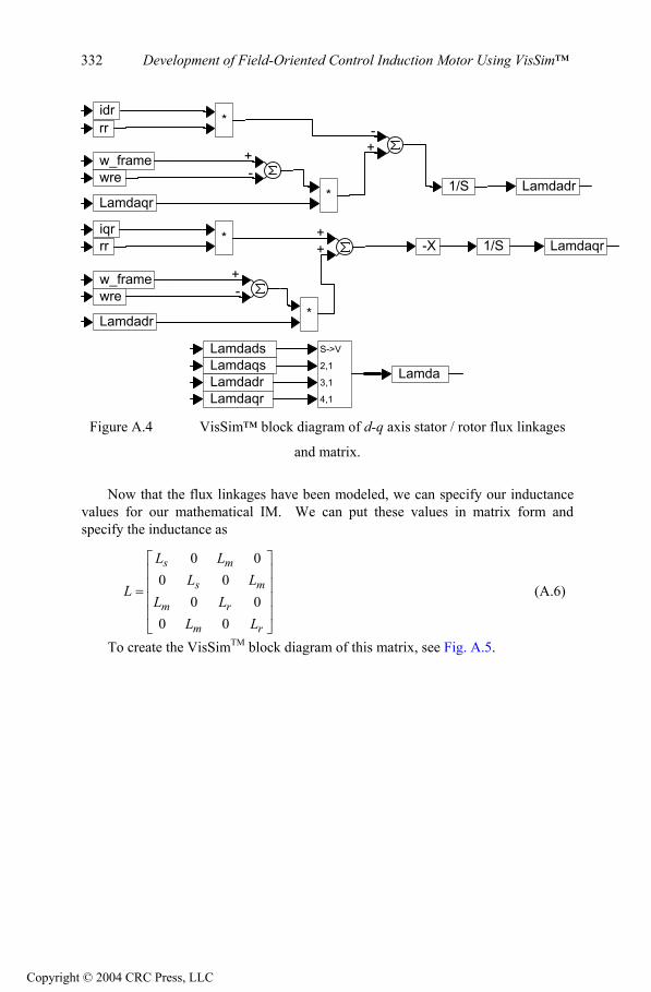
332 Development of Field-Oriented Control Induction Motor Using VisSim™
*rr
+-
*
-+
1/S LamdadrLamdaqr
wrew_frame
idr
++
*
+-
rr * -X 1/S Lamdaqriqr
w_framewre
Lamdadr
S->V
2,1
3,1
4,1
Lamda
LamdadsLamdaqsLamdadrLamdaqr
Figure A.4 VisSim™ block diagram of d-q axis stator / rotor flux linkages
and matrix.
Now that the flux linkages have been modeled, we can specify our inductancevalues for our mathematical IM. We can put these values in matrix form andspecify the inductance as
(A.6)
rm
rm
ms
ms
LLLL
LLLL
L
0000
0000
To create the VisSimTM block diagram of this matrix, see Fig. A.5.
Copyright © 2004 CRC Press, LLC

Development of Field-Oriented Control Induction Motor Using VisSim™ 333
S->V
1,2
1,3
1,4
2,1
2,2
2,3
2,4
3,1
3,2
3,3
3,4
4,1
4,2
4,3
4,4
0
0
0
00
0
Ls
LmLm
Lr
Lm
Lr
[ ] -1 inv_L
Ls0Lm0
L
Figure A.5 VisSim™ block diagram of stator, rotor, and mutual inductances
in matrix form.
Now that we have defined our flux linkages and inductances, we can define theelectrical torque and rotor speed equations as follows:
(A.7)
qs
dr
qs
ds
rm
rm
m
ms
qs
dr
qs
ds
iiii
LLLL
LLsLL
*
0000
0000
qsdsdsqse iiPT 2
3 (A.8)
Lere TT J
Pd 2
(A.9)
P
Pre
rm
rerm
60
2
min/
/
rev
srad (A.10)
We also need to specify the motor parameters listed in the beginning of this section. The block diagram in Fig. A.6 shows the motor parameters and otherconstants used with the simulation of the IM.
Copyright © 2004 CRC Press, LLC

334 Development of Field-Oriented Control Induction Motor Using VisSim™
.531
.408
.00252
.00252
.00847
.01099
rsrrLlsLlrLmLsLr.01099JP
.14
0 Tload
3.14159265358979 pi
.4 lamda_r*
Vdc250
.001 Ts
Figure A.6 Motor parameters and other constants used in simulation.
We can now model the electromechanical torque and speed of the motor in oursimulation. The block diagram in Fig. A.7 models the torque and speed of the IMwith respect to the other parameters modeled.
[ ]X[ ]
w_frame
idriqr
Lamdadr1Lamdaqr1
*
*
+-
*P
Tload+- *
P /lr
J
.5 dwre
*wre0
Lamdads1Lamdaqs1
.75
Lamda
Lamda
inv_L
V->S
2,1
3,1
4,1
V->S
2
3
4
idseiqse
S->V
2,1idqs
TE
dwre 1/S wre 60 /lr
P /lr wrm
pi
Figure A.7 Block diagram of the stator and rotor flux linkages, electromechanical
torque, and speed.
Copyright © 2004 CRC Press, LLC

Development of Field-Oriented Control Induction Motor Using VisSim™ 335
A.3.2 Field Oriented Control (FOC) Block
We will now discuss the details of the FOC block sub-system region of Fig. A.3. Like the IM block discussed previously the FOC is composed of many discretefunctional blocks made into a compound block. This compound block is thenconnected with other discrete blocks to form the control sub-system shown in Fig. A.8.
Rotor_FO_Controller
wre.
S->V
2,1idqse*
wrm
+- 1
5s+50
swref
P/2
PI Controller
Tem*
Figure A.8 The rotor field oriented control (FOC) sub-system.
There are two inputs to the FOC sub-system: wre and Tem*. The respectiveoutputs of the FOC sub-system are the command values, iqse* and idse*. These arein the field-oriented rotor reference frame. The fundamental intention of this designis that the FOC will cause the rotor to generate a speed profile that follows the commanded speed input, wref. To do this, the commanded speed signal is first fed into the system where it is subtracted from the measured speed of the rotor. Theerror generated is then fed into a torque controller block. The torque control is doneby the PI controller that generates the torque command Tem*. This torquecommand is used to set the electromagnetic torque induced within the inductionmotor by calculating an appropriate iqse* command based on the generated Tem*,along with the user defined parameters lamda_r*, and theta_r (the integral of thespeed of the rotor). These values are then fed into the Rotor_FO_controllercompound block. The insides of the Rotor_FO_Controller block are shown in Fig.A.9.
Copyright © 2004 CRC Press, LLC

336 Development of Field-Oriented Control Induction Motor Using VisSim™
lamda_r*
*LmLs
*Lr
/lr idse*
1/XLrLs 1/X -X
++
*lamda_r* idr*
T*
P .75
LmLr /
lr
lamda_r*
/lr iqse*
iqse*
-XLm*
/lrLr iqr*
lamda_r*rr /
lr
iqse*
/lrLr
Lm*
*
Wslip*
Wslip* 1/S
e_wre 1/S++ rho
theta_r
theta_slip
Figure A.9 Inside the Rotor_FO_Controller compound block.
The Rotor_FO_Controller block mathematically calculates the values of iqse*,idse*, the angle rho which is sum of the slip angle, theta_slip, and the rotor angletheta_r. These are the outputs of this block and are the inputs for the next blocks.The Rotor_FO_controller and the other blocks shown above regulate the sinusoidalcurrents applied to the current controllers according to the commandedelectromagnetic torque, Tem*, and the constant rotor flux, lamda_r*. The nextblock utilizes the inverse Clarke and Park transformations. These methods are usedto transform values referenced along the rotating reference frame into valuesreferenced in the stationary frame. Isd and isq are then used to set the magnitude ofthe current sinusoidal values.
Copyright © 2004 CRC Press, LLC

Development of Field-Oriented Control Induction Motor Using VisSim™ 337
A.3.3 The dq* dq Sub-System
The dq* dq sub-system in Fig. A.3 consists of the dq* dq block and the two PI controllers which feed the block. The two PI controllers shown in Fig. A.10output the desired command values for the dq-axis stator voltages (Vdse* and Vqse*).
idqss*
idqse* +-
5s+.5
sV->S
2,1
5s+.5
s
Vdse*
Vqse*
PI Controllers
Figure A.10 PI blocks after FOC compound block output.
The command values for the dq-axis stator voltages (Vdse* and Vqse*) are thenused in (A.11) to determine Vqss* and Vdss*. Equation (A.12) is implemented viathe dq* dq block. The insides of the dq* dq block are also shown in Fig. A.11.
cossin
sincos***
***
eds
eqs
sds
eds
eqs
sqs
vvv
vvv (A.11)
rho cos
sin
Vdse*Vqse*
-X
S->V
2,1
S->V
2,1
*
*
++
Vdss*V->S
2,1 Vqss*
Figure A.11 Command values for dq-axis stator voltages (dq* dq block).
A.3.4 The Space Vector PWM (SVPWM) Sub-System
The SVPWM subsystem is the SVPWM block shown in Fig. A.3. This sub-system generates the a-b-c stator voltages and then converts them into the d-qreference frame voltages for use by the induction motor model. The block diagramin Fig. A.12 contains the SVPWM block.
Copyright © 2004 CRC Press, LLC

338 Development of Field-Oriented Control Induction Motor Using VisSim™
SVPWM
c1
c2
c3
Vdss*
Vqss*
sw11
sw22
sw33
Figure A.12 Voltage-fed six-step space-vector PWM inverter.
+++
-X-X
2c1c2c3
*Vdc /lr3 Va1
Vb13 /lrVdc *
c3c1c2 2
-X-X
+++
Vc13 /lrVdc *
c1c2c3 2
-X-X
+++
Figure A.13 Generation of a-b-c motor stator voltages from SVPWM.
Because the induction motor model equations use the d-q voltages, it isnecessary to translate the a-b-c voltages (which would normally be fed into a realmotor) into the d-q frame. This task is done by the block diagram in Fig. A.14.
Vabc->Vdqs
1/Sw_frame
Va1Vb1Vc1
Figure A.14 Transformation block of a-b-c voltages to d-q reference frame
voltages for induction motor.
Copyright © 2004 CRC Press, LLC

Development of Field-Oriented Control Induction Motor Using VisSim™ 339
The inside of the Vabc Vdqs compound block is shown in Fig. A.15.
sin
++
*
-2.09439510239320
++
sin * ++
.66666666666
* Vds
thetaVa
Vbtheta
theta Vc *sin2.09439510239320++
++2.09439510239320
*Vctheta
theta Vb
Vatheta
Vqs*
.66666666666
++
*
++
-2.09439510239320
*
++
cos
cos
cos
Figure A.15 Inside of the Vabcs Vdqs block in Fig. A.14.
A.3.5 Feedback Sub-System
The feedback sub-system consists of both the dq ab block and dq* dqblocks. Stator current transformation from dqe to dqs is given in the block diagrambelow. Equation (A.12) models the idss* and iqss* variables. The equations areimplemented in the block diagram shown in Fig. A.16.
(A.12)cossin
sincos*
*
eds
eqs
sds
eds
eqs
sqs
iii
iii
idqss*++
*
*
S->V
2,1
S->V
2,1
-X
iqseidse
sin
cosrho
Figure A.16 Command values for the dq-axis stator currents (dq_dq* block).
Copyright © 2004 CRC Press, LLC

340 Development of Field-Oriented Control Induction Motor Using VisSim™
A.3.6 Simulation Results
Speed Response Analysis The speed response of our designed control system is of the utmost significance
to this section of the design. By feeding an input speed command into the system, we observe the speed developed by the rotor of the induction machine over time. The two major criteria that we are trying to fulfill are:
1. the system develops a speed response that closely resembles the input speed command
2. the system is stable because stability is the most important design specification for any control system [2]
Once these two criteria are met, we would also like to achieve a quick transient response, i.e., quick acceleration and a response that is smooth.
Analysis of the Field-Orientated Section of the Design
To increase the speed of the rotor we have to increase the voltage and frequency by the same proportion. This ensures that we maintain a constant magnetic flux in the air-gap of the induction motor. In this section of the design, through the use of scopes placed on nodes of interest, we see that FOC applies this principle of speed operation. FOC transforms the commanded dc signals applied by the user and the feedback signals into sinusoidal signals required by the IM.
FOC is also referred to as vector control because it controls both the magnitude and phase of the voltage signal applied to the stator windings of the IM. The manner in which the phase changes over time for the cos_rho and sin_rho signals is very similar to the way the phase voltage signal develops over time. The phase voltage signal has a similar profile. Thus, the cos_rho and sin_rho signals control the phase, while the iqs and ids signals control the magnitude. It is through these signals, all of which are produced in the Rotor_FO_controller block, that FOC achieves vector control. Furthermore, the speed is linearly increased when the frequency and amplitude of the phase voltage signal is increased by the same proportion.
The principle of increasing the voltage magnitude and the frequency by the same proportion in order to maintain a constant rotor flux is the basis for applying scalar volts per hertz speed control method. However, the equations used to execute FOC consider the parameters of the motor. Therefore, we achieve better control over torque variations. FOC also has the advantage of extending the speed range of operation through field weakening. Finally, FOC is a torque control method. This suits the requirements of the induction motor control design. Figure A.17 shows the electromagnetic torque developed for a ramp speed command. The actual speed is depicted in Fig. A.18.
Copyright © 2004 CRC Press, LLC

Development of Field-Oriented Control Induction Motor Using VisSim™ 341
Electromagnetic Torque
Time (sec)0 .25 .5 .75 1 1.25 1.5 1.75 2 2.25 2.5 2.75 3 3.25 3.5 3.75 4 4.25 4.5 4.75 5
Torq
ue (N
m)
-4.0
-3.5
-3.0
-2.5
-2.0
-1.5
-1.0
-.5
0
.5
1.0
1.5
2.0
2.5
3.0
3.5
4.0
4.5
5.0
Figure A.17 Electromagnetic torque result from VisSim™ simulation.
Rotor Speed (wre)
Time (sec)0 .25 .5 .75 1 1.25 1.5 1.75 2 2.25 2.5 2.75 3 3.25 3.5 3.75 4 4.25 4.5 4.75 5
Rot
or S
peed
(rad
/s)
-100
-80
-60
-40
-20
0
20
40
60
80
100
120
140
160
180
200
Figure A.18 Rotor speed result from VisSim™ simulation.
A.4 Summary and Improvements
In this appendix, the simulation of a field-oriented IM using VisSim™ waspresented. The electromagnetic torque and rotor speed were given. We presentedthe concept of FOC to be the control technique because it produced controlledresults that had better dynamic response to torque variations in a wider speed rangecompared to other scalar methods. It was shown through the VisSim™ analysis that
Copyright © 2004 CRC Press, LLC

342 Development of Field-Oriented Control Induction Motor Using VisSim™
FOC is an effective means of driving an induction motor. Also, a speed profile with an adequate transient response and steady-state error was generated.
By simulating the control system, we obtained an acceptable speed response and found there was adequate stability. It is also worthy to note that increasing the proportional gain of the torque controller introduced or amplified noise and harmonics. This affected the short-term and long-term performance of the induction machine. Also, by increasing the proportional gain of the torque controller, the system approached unstable regions of operation.
An improvement on the system could include the implementation of a self-tuning FOC module. In the self-tuning scheme, any change in resistance of the stator and rotor windings due to heat could be accounted for.
References
1. P. Vas, Vector Control of ac Machines, Oxford University Press, New York, 1990.
2. D.W. Novotny and T.A. Lipo, Vector Control and Dynamics of AC Drives,Oxford University Press, New York, 1996.
3. N. Mohan, T.M. Undeland, and W.P. Robbins, Power Electronics: Circuits, Devices, and Applications - 2nd ed., John Wiley & Sons, New York, 1995.
4. B. K. Bose, Adjustable Speed ac Drive Systems, IEEE Press, New York, 1987. 5. C-M. Ong, Dynamic Simulation of Electric Machinery using MATLAB
/SIMULINK, Prentice Hall, New Jersey, 1998. 6. Texas Instruments Inc., Field Orientated Control of 3-Phase AC-Motors,
www.ti.com, Texas Instruments Literature number BPRA073, Europe, 1998. 7. Texas Instruments Inc., Clarke and Park Transforms on the TMS320C2xx,
www.ti.com, Texas Instruments Literature number BPRA048, Europe, 1998. 8. Texas Instruments Inc., Digital Signal Processing Solution for AC Induction
Motor, www.ti.com, Texas Instruments Literature number BPRA043, Europe, 1997.
9. Texas Instruments Inc., Implementation of a Speed Field Orientated Control of a Three-Phase AC Induction Motor, www.ti.com, Texas Instruments Literature number BPRA076, Europe, 2000.
10. Visual Solutions, Inc., VisSim™ 4.5g Fixed-Point Datasheet. 11. Visual Solutions, Inc., VisSim™ 4.5/TI C2000 Rapid Prototyper Datasheet.
Copyright © 2004 CRC Press, LLC


![Electromechanical wave imaging and electromechanical wave … · 2019-07-23 · motion and strain estimation based on Bmode [9] or radio-frequency (RF) ultrasound signals [10–13]](https://img.dokumen.tips/doc/110x75/5e9f95fa3886094c5e322e3d/electromechanical-wave-imaging-and-electromechanical-wave-2019-07-23-motion-and.jpg)