Embed Size (px)
Citation preview
Copyright 1995 by Dallas Semiconductor Corporation.All Rights Reserved. For important information regardingpatents and other intellectual property rights, please refer toDallas Semiconductor data books.
DS5002FPSecure Microprocessor Chip
DS5002FP
111996 1/28
48
FEATURES
• 8051 compatible microprocessor for secure/sensitiveapplications
– Access 32K, 64K, or 128K bytes of nonvolatileSRAM for program and/or data storage
– In–system programming via on–chip serial port– Capable of modifying its own program or data
memory in the end system
• Firmware Security Features:
– Memory stored in encrypted form– Encryption using on–chip 64–bit key– Automatic true random key generator– SDI Self Destruct Input– Optional top coating prevents microprobe
(DS5002FPM)– Improved security over previous generations– Protects memory contents from piracy
• Crashproof Operation
– Maintains all nonvolatile resources for over 10years in the absence of power
– Power–fail Reset– Early Warning Power–fail Interrupt– Watchdog Timer
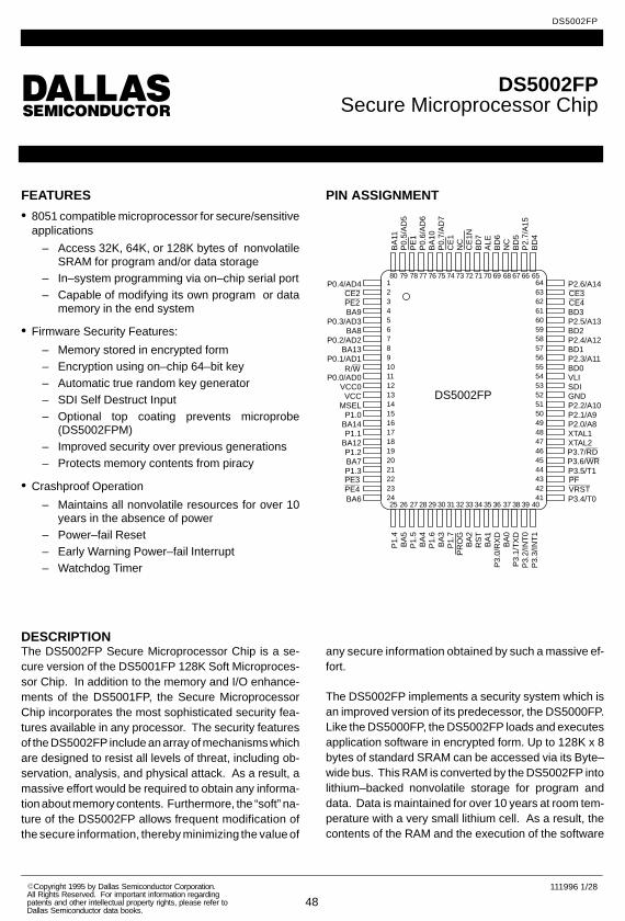
PIN ASSIGNMENT
R/W
P3.6/WRP3.7/RD
VRSTPF
CE3CE4
PE3PE4
PE2CE2
123456789101112131415161718192021222324
646362616059585756555453525150494847464544434241
80 79 78 77 76 7475 73 72 71 70 69 68 67 66 65
25 26 27 28 29 30 31 4032 33 34 35 36 37 38 39
DS5002FP
P2.6/A14
BD3P2.5/A13BD2P2.4/A12BD1P2.3/A11BD0VLISDIGNDP2.2/A10P2.1/A9P2.0/A8XTAL1XTAL2
P3.5/T1
P3.4/T0
P0.4/AD4
BA9P0.3/AD3
BA8P0.2/AD2
BA13P0.1/AD1
P0.0/AD0VCC0
VCCMSEL
P1.0BA14P1.1
BA12P1.2BA7P1.3
BA6
P1.
4B
A5
P1.
5B
A4
P1.
6B
A3
P1.
7P
RO
GB
A2
RS
TB
A1
P3.
0/R
XD
BA
0P
3.1/
TX
DP
3.2/
INT
0P
3.3/
INT
1
BA
11P
0.5/
AD
5P
E1
P0.
6/A
D6
BA
10P
0.7/
AD
7C
E1
NC
CE
1NB
D7
ALE
BD
6N
CB
D5
P2.
7/A
15B
D4
DESCRIPTIONThe DS5002FP Secure Microprocessor Chip is a se-cure version of the DS5001FP 128K Soft Microproces-sor Chip. In addition to the memory and I/O enhance-ments of the DS5001FP, the Secure MicroprocessorChip incorporates the most sophisticated security fea-tures available in any processor. The security featuresof the DS5002FP include an array of mechanisms whichare designed to resist all levels of threat, including ob-servation, analysis, and physical attack. As a result, amassive effort would be required to obtain any informa-tion about memory contents. Furthermore, the “soft” na-ture of the DS5002FP allows frequent modification ofthe secure information, thereby minimizing the value of
any secure information obtained by such a massive ef-fort.
The DS5002FP implements a security system which isan improved version of its predecessor, the DS5000FP.Like the DS5000FP, the DS5002FP loads and executesapplication software in encrypted form. Up to 128K x 8bytes of standard SRAM can be accessed via its Byte–wide bus. This RAM is converted by the DS5002FP intolithium–backed nonvolatile storage for program anddata. Data is maintained for over 10 years at room tem-perature with a very small lithium cell. As a result, thecontents of the RAM and the execution of the software

DS5002FP
111996 2/28
49
appear unintelligible to the outside observer. The en-cryption algorithm uses an internally stored and pro-tected key. Any attempt to discover the key value re-sults in its erasure, rendering the encrypted contents ofthe RAM useless.
The Secure Microprocessor Chip offers a number ofmajor enhancements to the software security imple-mented in the previous generation DS5000FP. First, theDS5002FP provides a stronger software encryption al-gorithm which incorporates elements of DES encryp-tion. Second, the encryption is based on a 64–bit keyword, as compared to the DS5000FP’s 40–bit key.Third, the key can only be loaded from an on–chip truerandom number generator. As a result, the true key val-ue is never known by the user. Fourth, a Self–Destructinput pin (SDI) is provided to interface to external tam-per detection circuitry. With or without the presence ofVCC, activation of the SDI pin has the same effect as re-setting the Security Lock: immediate erasure of the keyword and the 48–byte Vector RAM area. Fifth, an op-tional top–coating of the die prevents access of in-formation using microprobing techniques. Finally, cus-tomer–specific versions of the DS5002FP are availablewhich incorporate a one–of–a–kind encryption algo-rithm.
When implemented as a part of a secure system de-sign, a system based on the DS5002FP can typicallyprovide a level of security which requires more time andresources to defeat than it is worth to unauthorized indi-viduals who have reason to try. For a user who wants a
pre–constructed module using the DS5002FP, RAM,lithium cell, and a real time clock, the DS2252T is avail-able and described in a separate data sheet.
ORDERING INFORMATIONThe following devices are available as standard prod-ucts from Dallas Semiconductor:
PART # DESCRIPTION
DS5002FP–16 80–pin QFP,Max. clock speed 16 MHz,0°C to 70°C operation
DS5002FPM–16 80–pin QFP,Max. clock speed 16 MHz,0°C to 70°C operation,Internal microprobe shield
Operating information is contained in the User’s GuideSection of the Secure Microprocessor Data Book. Thisdata sheet provides ordering information, pin–out, andelectrical specifications.
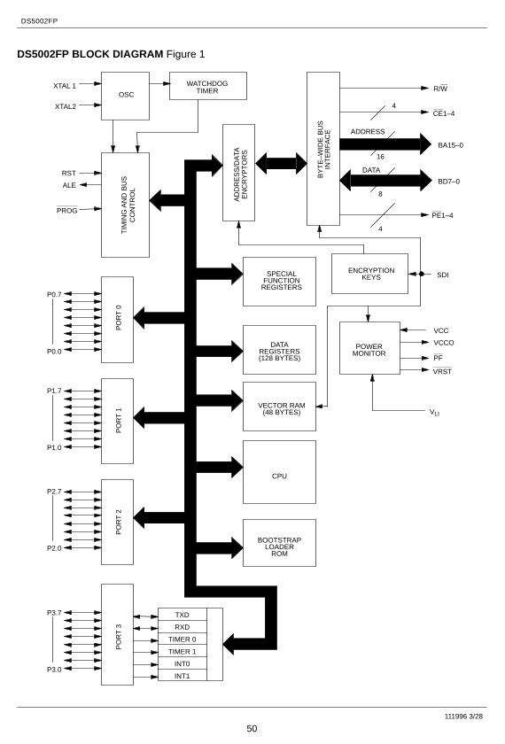
BLOCK DIAGRAMFigure 1 is a block diagram illustrating the internal archi-tecture of the DS5002FP. The DS5002FP is a secureimplementation of the DS5001FP 128K Soft Micropro-cessor Chip. As a result, It operates in an identical fash-ion to the DS5001FP except where indicated. See theDS5001FP Data Sheet for operating details.
PF
VRST
PROG
OSC
WATCHDOGTIMER
XTAL 1
XTAL2
RST
ALE
P0.7
P0.0
P1.7
P1.0
P2.7
P2.0
P3.7
P3.0
SPECIALFUNCTION
REGISTERS
DATAREGISTERS(128 BYTES)
VECTOR RAM(48 BYTES)
CPU
BOOTSTRAPLOADER
ROM
ENCRYPTIONKEYS
POWERMONITOR
TXD
RXD
TIMER 0
TIMER 1
INT0
INT1
PO
RT
3P
OR
T 2
PO
RT
1P
OR
T 0
TIM
ING
AN
D B
US
CO
NT
RO
L
AD
DR
ES
S/D
ATA
EN
CR
YP
TO
RS
BY
TE
–WID
E B
US
INT
ER
FAC
E
VLI
VCC
VCCO
SDI
R/W
CE1–4
BA15–0
BD7–0
PE1–4
ADDRESS
DATA
16
8
4
4
DS5002FP
111996 3/28
50
DS5002FP BLOCK DIAGRAM Figure 1

DS5002FP
111996 4/28
51
PIN DESCRIPTION
PIN DESCRIPTION
11, 9, 7, 5, 1,79, 77, 75
P0.0 – P0.7. General purpose I/O Port 0. This port is open–drain and can not drive a logic 1. Itrequires external pull–ups. Port 0 is also the multiplexed Expanded Address/Data bus. Whenused in this mode, it does not require pull–ups.
15, 17, 19,21, 25, 27,
29, 31
P1.0 – P1.7. General purpose I/O Port 1.
49, 50, 51,56, 58, 60,
64, 66
P2.0 – P2.7. General purpose I/O Port 2. Also serves as the MSB of the Expanded Address bus.
36 P3.0 RXD. General purpose I/O port pin 3.0. Also serves as the receive signal for the on boardUART. This pin should NOT be connected directly to a PC COM port.
38 P3.1 TXD. General purpose I/O port pin 3.1. Also serves as the transmit signal for the on boardUART. This pin should NOT be connected directly to a PC COM port.
39 P3.2 INT0. General purpose I/O port pin 3.2. Also serves as the active low ExternalInterrupt 0.
40 P3.3 INT1. General purpose I/O port pin 3.3. Also serves as the active low ExternalInterrupt 1.
41 P3.4 T0. General purpose I/O port pin 3.4. Also serves as the Timer 0 input.
44 P3.5 T1. General purpose I/O port pin 3.5. Also serves as the Timer 1 input.
45 P3.6 WR. General purpose I/O port pin. Also serves as the write strobe for Expanded bus opera-tion.
46 P3.7 RD. General purpose I/O port pin. Also serves as the read strobe for Expanded bus opera-tion.
34 RST – Active high reset input. A logic 1 applied to this pin will activate a reset state. This pin ispulled down internally so this pin can be left unconnected if not used. An RC power–on reset cir-cuit is not needed and is NOT recommended.
70 ALE – Address Latch Enable. Used to de–multiplex the multiplexed Expanded Address/Data buson Port 0. This pin is normally connected to the clock input on a ’373 type transparent latch.
47, 48 XTAL2, XTAL1. Used to connect an external crystal to the internal oscillator. XTAL1 is the inputto an inverting amplifier and XTAL2 is the output.
52 GND – Logic ground.
13 VCC – +5V
12 VCCO – VCC Output. This is switched between VCC and VLI by internal circuits based on the levelof VCC. When power is above the lithium input, power will be drawn from VCC. The lithium cellremains isolated from a load. When VCC is below VLI, the VCCO switches to the VLI source. VCCOshould be connected to the VCC pin of an SRAM.
54 VLI – Lithium Voltage Input. Connect to a lithium cell greater than VLImin and no greater thanVLImax as shown in the electrical specifications. Nominal value is +3V.
16, 8, 18, 80,76, 4, 6, 20,24, 26, 28,
30, 33, 35, 37
BA14 – 0. Byte–wide Address bus bits 14–0. This bus is combined with the non–multiplexed databus (BD7–0) to access NVSRAM. Decoding is performed using CE1 through CE4. Therefore,BA15 is not actually needed. Read/write access is controlled by R/W. BA14–0 connect directlyto an 8K, 32K, or 128K SRAM. If an 8K RAM is used, BA13 and BA14 will be unconnected. If a128K SRAM is used, the micro converts CE2 and CE3 to serve as A16 and A15 respectively.

DS5002FP
111996 5/28
52
PIN DESCRIPTION
71, 69, 67,65, 61, 59,
57, 55
BD7 – 0. Byte–wide Data bus bits 7–0. This 8–bit bi–directional bus is combined with the non–multiplexed address bus (BA14–0) to access NV SRAM. Decoding is performed on CE1 andCE2. Read/write access is controlled by R/W. BD7–0 connect directly to an SRAM, and optionallyto a Real–time Clock or other peripheral.
10 R/W – Read/Write. This signal provides the write enable to the SRAMs on the Byte–wide bus.It is controlled by the memory map and Partition. The blocks selected as Program (ROM) will bewrite protected.
74 CE1 – Chip Enable 1. This is the primary decoded chip enable for memory access on the Byte–wide bus. It connects to the chip enable input of one SRAM. CE1 is lithium backed. It will remainin a logic high inactive state when VCC falls below VLI.
2 CE2 – Chip Enable 2. This chip enable is provided to access a second 32K block of memory.It connects to the chip enable input of one SRAM. When MSEL=0, the micro converts CE2 intoA16 for a 128K x 8 SRAM. CE2 is lithium backed and will remain at a logic high when VCC fallsbelow VLI.
63 CE3 – Chip Enable 3. This chip enable is provided to access a third 32K block of memory. It con-nects to the chip enable input of one SRAM. When MSEL=0, the micro converts CE3 into A15for a 128K x 8 SRAM. CE3 is lithium backed and will remain at a logic high when VCC falls belowVLI.
62 CE4 – Chip Enable 4. This chip enable is provided to access a fourth 32K block of memory. Itconnects to the chip enable input of one SRAM. When MSEL=0, this signal is unused. CE4 islithium backed and will remain at a logic high when VCC falls below VLI.
78 PE1 – Peripheral Enable 1. Accesses data memory between addresses 0000h and 3FFFh whenthe PES bit is set to a logic 1. Commonly used to chip enable a Byte–wide Real Time Clock suchas the DS1283. PE1 is lithium backed and will remain at a logic high when VCC falls below VLI.Connect PE1 to battery backed functions only.
3 PE2 – Peripheral Enable 2. Accesses data memory between addresses 4000h and 7FFFh whenthe PES bit is set to a logic 1. PE2 is lithium backed and will remain at a logic high when VCCfalls below VLI. Connect PE2 to battery backed functions only.
22 PE3 – Peripheral Enable 3. Accesses data memory between addresses 8000h and BFFFh whenthe PES bit is set to a logic 1. PE3 is not lithium backed and can be connected to any type ofperipheral function. If connected to a battery backed chip, it will need additional circuitry to main-tain the chip enable in an inactive state when VCC < VLI.
23 PE4 – Peripheral Enable 4. Accesses data memory between addresses C000h and FFFFh whenthe PES bit is set to a logic 1. PE4 is not lithium backed and can be connected to any type ofperipheral function. If connected to a battery backed chip, it will need additional circuitry to main-tain the chip enable in an inactive state when VCC < VLI.
32 PROG – Invokes the Bootstrap Loader on a falling edge. This signal should be debounced sothat only one edge is detected. If connected to ground, the micro will enter Bootstrap loading onpower up. This signal is pulled up internally.
42 VRST – This I/O pin (open drain with internal pull–up) indicates that the power supply (VCC) hasfallen below the VCCmin level and the micro is in a reset state. When this occurs, the DS5002FPwill drive this pin to a logic 0. Because the micro is lithium backed, this signal is guaranteed evenwhen VCC=0V. Because it is an I/O pin, it will also force a reset if pulled low externally. This allowsmultiple parts to synchronize their power–down resets.
43 PF – This output goes to a logic 0 to indicate that the micro has switched to lithium backup. Thiscorresponds to VCC < VLI. Because the micro is lithium backed, this signal is guaranteed evenwhen VCC=0V. The normal application of this signal is to control lithium powered current to isolatebattery backed functions from non–battery backed functions.

DS5002FP
111996 6/28
53
PIN DESCRIPTION
14 MSEL – Memory select. This signal controls the memory size selection. When MSEL= +5V, theDS5002FP expects to use 32K x 8 SRAMs. When MSEL = 0V, the DS5002FP expects to usea 128K x 8 SRAM. MSEL must be connected regardless of Partition, Mode, etc.
53 SDI – Self–Destruct Input. An active high on this pin causes an unlock procedure. This resultsin the destruction of Vector RAM, Encryption Keys, and the loss of power from VCCO. This pinshould be grounded if not used.
72 CE1N – This is a non–battery backed version of CE1. It is not generally useful since theDS5002FP can not be used with EPROM due to its encryption.
73 NC – Do not connect.
SECURE OPERATION OVERVIEWThe DS5002FP incorporates encryption of the activityon its Byte–wide Address/Data bus to prevent unautho-rized access to the program and data information con-tained in the nonvolatile RAM. Loading an applica-tion program in this manner is performed via theBootstrap Loader using the general sequence de-scribed below:
1. Clear Security Lock2. Set memory map configuration as for DS5001FP3. Load application software4. Set Security Lock5. Exit Loader
Loading of application software into the program/dataRAM is performed while the DS5002FP is in its Boot-strap Load mode. Loading is only possible when the Se-curity Lock is clear. If the Security Lock has previouslyset, then it must be cleared by issuing the “Z” commandfrom the Bootstrap Loader. Resetting the Security Lockinstantly clears the previous key word and the contentsof the Vector RAM. In addition, the Bootstrap ROMwrites zeroes into the first 32K of external RAM.
The user’s application software is loaded into externalCMOS SRAM via the “L” command in “scrambled” formthrough on–chip encryptor circuits. Each external RAMaddress is an encrypted representation of an on–chiplogical address. Thus, the sequential instructions of anordinary program or data table are stored non–sequen-tially in RAM memory. The contents of the program/dataRAM are also encrypted. Each byte in RAM is en-crypted by a key– and address–dependent encryptorcircuit such that identical bytes are stored as differentvalues in different memory locations.
The encryption of the program/data RAM is dependenton an on–chip 64–bit key word. The key is loaded bythe ROM firmware just prior to the time that the applica-
tion software is loaded, and is retained as nonvolatileinformation in the absence of VCC by the lithium backupcircuits. After loading is complete, the key is protectedby setting the on–chip Security Lock, which is also re-tained as nonvolatile information in the absence of VCC.Any attempt to tamper with the key word and therebygain access to the true program/data RAM contents re-sults in the erasure of the key word as well as the RAMcontents.
During execution of the application software, logical ad-dresses on the DS5002FP that are generated from theprogram counter or data pointer registers are encryptedbefore they are presented on the Byte–wide AddressBus. Opcodes and data are read back and decryptedbefore they are operated on by the CPU. Similarly, datavalues written to the external nonvolatile RAM storageduring program execution are encrypted before they arepresented on the Byte–wide data bus during the writeoperation. This encryption/decryption process is per-formed in real time such that no execution time is lost ascompared to the non–encrypted DS5001FP or 8051running at the same clock rate. As a result, operation ofthe encryptor circuitry is transparent to the applicationsoftware.
Unlike the DS5000FP, the DS5002FP chip’s securityfeature is always enabled.
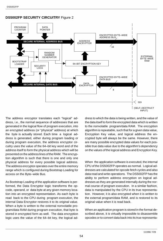
SECURITY CIRCUITRYThe on–chip functions associated with the DS5002FP’ssoftware security feature are depicted in Figure 2. En-cryption logic consists of an address encryptor and adata encryptor. Although each encryptor uses its ownalgorithm for encrypting data, both depend on the64–bit key word which is contained in the EncryptionKey registers. Both the encryptors operate during load-ing of the application software and also during itsexecution.
DS5002FP
111996 7/28
54
DS5002FP SECURITY CIRCUITRY Figure 2
DATAPOINTER
BOOTSTRAPLOADER
EXTERNALBYTE–WIDE
RAM
16
PROGRAMCOUNTER
ADDRESSENCRYPTOR
SECURITYLOCK
8
64–BIT ENCRYPTION KEY
DATAENCRYPTOR
SDI
(SELF–DESTRUCTINPUT)
RANDOMNUMBER
GENERATOR
ENCRYPTED BYTE–WIDEADDRESS BUS
ENCRYPTED BYTE–WIDEDATA BUS
SECURE INTERNAL DATE BUS
SECURE INTERNAL ADDRESS BUS
The address encryptor translates each “logical” ad-dress, i.e., the normal sequence of addresses that aregenerated in the logical flow of program execution, intoan encrypted address (or “physical” address) at whichthe byte is actually stored. Each time a logical ad-dress is generated, either during program loading orduring program execution, the address encryptor cir-cuitry uses the value of the 64–bit key word and of theaddress itself to form the physical address which will bepresented on the address lines of the RAM. The encryp-tion algorithm is such that there is one and only onephysical address for every possible logical address.The address encryptor operates over the entire memoryrange which is configured during Bootstrap Loading foraccess on the Byte–wide Bus.
As Bootstrap Loading of the application software is per-formed, the Data Encryptor logic transforms the op-code, operand, or data byte at any given memory loca-tion into an encrypted representation. As each byte isread back to the CPU during program execution, theinternal Data Encryptor restores it to its original value.When a byte is written to the external nonvolatile pro-gram/data RAM during program execution, that byte isstored in encrypted form as well. The data encryptionlogic uses the value of the 64–bit key, the logical ad-
dress to which the data is being written, and the value ofthe data itself to form the encrypted data which is writtento the nonvolatile program/data RAM. The encryptionalgorithm is repeatable, such that for a given data value,Encryption Key value, and logical address the en-crypted byte will always be the same. However, thereare many possible encrypted data values for each pos-sible true data value due to the algorithm’s dependencyon the values of the logical address and Encryption Key.
When the application software is executed, the internalCPU of the DS5002FP operates as normal. Logical ad-dresses are calculated for opcode fetch cycles and alsodata read and write operations. The DS5002FP has theability to perform address encryption on logical ad-dresses as they are generated internally during the nor-mal course of program execution. In a similar fashion,data is manipulated by the CPU in its true representa-tion. However, it is also encrypted when it is written tothe external program/data RAM, and is restored to itsoriginal value when it is read back.
When an application program is stored in the format de-scribed above, it is virtually impossible to disassembleopcodes or to convert data back into its true representa-
DS5002FP
111996 8/28
55
tion. Address encryption has the effect that the op-codes and data are not stored in the contiguous form inwhich they were assembled, but rather in seeminglyrandom locations in memory. This in itself makes it virtu-ally impossible to determine the normal flow of the pro-gram. As an added protection measure, the AddressEncryptor also generates “dummy” read access cycleswhenever time is available during program execution.
DUMMY READ CYCLES Like the DS5000FP, the DS5002FP generates a“dummy” read access cycle to non–sequential address-es in external RAM memory whenever time is availableduring program execution. This action has the effect offurther complicating the task of determining the normalflow of program execution. During these pseudo–ran-dom dummy cycles, the RAM is read to all appearance,but the data is not used internally. Through the use of arepeatable exchange of dummy and true read cycles, itis impossible to distinguish a dummy cycle from a realone.
ENCRYPTION ALGORITHMThe DS5002FP incorporates a proprietary algorithm im-plemented in hardware which performs the scramblingof address and data on the Byte–wide bus to the staticRAM. This algorithm has been greatly strengthenedwith respect to its DS5000FP predecessor. Improve-ments include:
1. 64–bit Encryption Key
2. Incorporation of DES–like operations to provide agreater degree of nonlinearity
3. Customizable encryption
The encryption circuitry uses a 64–bit key value(compared to the DS5000FP’s 40–bit key) which isstored on the DS5002FP die and protected by the Secu-rity Lock function described below. In addition, the al-gorithm has been strengthened to incorporate certainoperations used in DES encryption, so that the encryp-tion of both the addresses and data is highly nonlinear.Unlike the DS5000FP, the encryption circuitry in theDS5002FP is always enabled.
Dallas Semiconductor can customize the encryption cir-cuitry by laser programming the die to insure that aunique encryption algorithm is delivered to the custom-er. In addition, the customer–specific version can bebranded as specified by the customer. Please contact
Dallas Semiconductor for ordering information of cus-tomer–specific versions.
ENCRYPTION KEYAs described above, the on–chip 64–bit Encryption Keyis the basis of both the address and data encryptor cir-cuits. The DS5002FP provides a key management sys-tem which is greatly improved over the DS5000FP. TheDS5002FP does not give the user the ability to select akey. Instead, when the loader is given certain com-mands, the key is set based on the value read from anon–chip hardware random number generator. This ac-tion is performed just prior to actually loading the codeinto the external RAM. This scheme prevents character-ization of the encryption algorithm by continuously load-ing new, known keys. It also frees the user from the bur-den of protecting the key selection process.
The random number generator circuit uses the asynch-ronous frequency differences of two internal ring oscil-lator and the processor master clock (determined byXTAL1 and XTAL2). As a result, a true random numberis produced.
VECTOR RAMA 48–byte Vector RAM area is incorporated on–chip,and is used to contain the reset and interrupt vectorcode in the DS5002FP. It is included in the architectureto help insure the security of the application program.
If reset and interrupt vector locations were accessedfrom the external nonvolatile program/data RAM duringthe execution of the program, then it would be possibleto determine the encrypted value of known addresses.This could be done by forcing an interrupt or resetcondition and observing the resulting addresses on theByte–wide address/data bus. For example, it is knownthat when a hardware reset is applied the logical pro-gram address is forced to location 0000H and code isexecuted starting from this location. It would then bepossible to determine the encrypted value (or physicaladdress) of the logical address value 0000H by observ-ing the address presented to the external RAM followinga hardware reset. Interrupt vector address relationshipscould be determined in a similar fashion. By using theon–chip Vector RAM to contain the interrupt and resetvectors, it is impossible to observe such relationships.Although it is very unlikely that an application programcould be deciphered by observing vector address rela-tionships, the Vector RAM eliminates this possibility.
DS5002FP
111996 9/28
56
Note that the dummy accesses mentioned above areconducted while fetching from Vector RAM.
The Vector RAM is automatically loaded with the user’sreset and interrupt vectors during bootstrap loading.
SECURITY LOCKOnce the application program has been loaded into theDS5002FP’s NV RAM, the Security Lock may be en-abled by issuing the “Z” command in the BootstrapLoader. While the Security Lock is set, no further ac-cess to program/ data information is possible via the on–chip ROM. Access is prevented by both the BootstrapLoader firmware and the DS5002FP encryptor circuits.
Access to the NVRAM may only be regained by clearingthe Security Lock via the “U” command in the BootstrapLoader. This action triggers several events which de-feat tampering. First, the Encryption Key is instanta-neously erased. Without the Encryption Key, theDS5002FP is no longer able to decrypt the contents ofthe RAM. Therefore, the application software can nolonger be correctly executed, nor can it be read back inits true form via the Bootstrap Loader. Second, the Vec-tor RAM area is also instantaneously erased, so that thereset and vector information is lost. Third, the BootstrapLoader firmware sequentially erases the encryptedRAM area. Lastly, the loader creates and loads a newrandom key.
The Security Lock bit itself is constructed using a multi-ple–bit latch which is interlaced for self–destruct in theevent of tampering. The lock is designed to set–up a“domino–effect” such that erasure of the bit will result inan unstoppable sequence of events that clears criticaldata including Encryption Key and Vector RAM. In addi-tion, this bit is protected from probing by the top–coatingfeature mentioned below.
SELF–DESTRUCT INPUTThe Self–Destruct Input (SDI) pin is an active high inputwhich is used to reset the Security Lock in response toan external event. The SDI input is intended to be usedwith external tamper detection circuitry. It can be acti-vated with or without operating power applied to the VCCpin. Activation of the SDI pin instantly resets the Securi-
ty Lock and causes the same sequence of events de-scribed above for this action. In addition, power is mo-mentarily removed from the Byte–wide bus interfaceincluding the VCCO pin, resulting in the loss of data in ex-ternal RAM.
TOP LAYER COATINGThe DS5002FPM is provided with a special top–layercoating that is designed to prevent a probe attack. Thiscoating is implemented with second–layer metal addedthrough special processing of the microcontroller die.This additional layer is not a simple sheet of metal, butrather a complex layout that is interwoven with powerand ground which are in turn connected to logic for theEncryption Key and the Security Lock. As a result, anyattempt to remove the layer or probe through it will re-sult in the erasure of the Security Lock and/or the loss ofEncryption Key bits.
BOOTSTRAP LOADINGInitial loading of application software into theDS5002FP is performed by firmware within the on–chipBootstrap Loader communicating with a PC via the on–chip serial port in a manner which is almost identical tothat for the DS5001FP. The user should consult theDS5001FP data sheet as a basis of operational charac-teristics of this firmware. Certain differences in loadingprocedure exist in order to support the security feature.These differences are documented below. Table 1 sum-marizes the commands accepted by the bootstraploader.
When the Bootstrap Loader is invoked, portions of the128–byte scratchpad RAM area are automatically over-written with zeroes, and then used for variable storagefor the bootstrap firmware. Also, a set of eight bytes aregenerated using the random number generator circuitryand are saved as a potential word for the 64–bit Encryp-tion Key.
Any read or write operation to the DS5002FP’s externalprogram/data SRAM can only take place if the SecurityLock bit is in a cleared state. Therefore, the first stepwhich is taken in the loading of a program should be theclearing of the Security Lock bit through the “U” com-mand.

DS5002FP
111996 10/28
57
DS5002FP SERIAL BOOTSTRAP LOADER COMMANDS Table 1
COMMAND FUNCTION
C Return CRC–16 of the program/data NV RAM
D Dump Intel Hex file
F Fill program/data NV RAM
G Get Data from P1, P2, and P3
I N/A on the DS5002FP
L Load Intel Hex file
M Toggle modem available bit
N Set Freshness Seal – All program and data will be lost
P Put data into P0, P1, P2, and P3
R Read status of NVSFRs (MCON, RPCTL, MSL, CALIB)
T Trace (echo) incoming Intel Hex code
U Clear Security Lock
V Verify program/data NV RAM with incoming Intel Hex data
W Write Special Function Registers – (MCON, RPCTL, MSL, CALIB)
Z Set Security Lock
Execution of certain Bootstrap Loader commands willresult in the loading of the newly generated 64–bit ran-dom number into the Encryption Key word. These com-mands are as follows:
Fill F
Load L
Dump D
Verify V
CRC C
Execution of the Fill and Load commands will result inthe data loaded into the NV RAM in an encrypted formdetermined by the value of the newly–generated keyword. The subsequent execution of the Dump com-mand within the same bootstrap session will cause thecontents of the encrypted RAM to be read out and trans-mitted back to the host PC in decrypted form. Similarly,execution of the Verify command within the same boot-strap session will cause the incoming absolute hex datato be compared against the true contents of the en-crypted RAM, and the CRC command will return theCRC value calculated from the true contents of the en-crypted RAM. As long as any of the above commandsare executed within the same bootstrap session, the
loaded key value will remain the same and contents ofthe encrypted program/data NV RAM may be read orwritten normally and freely until the Security Lock bit isset.
When the Security Lock bit is set using the Z command,no further access to the true RAM contents is possibleusing any bootstrap command or by any other means.
INSTRUCTION SETThe DS5002FP executes an instruction set that isobject code compatible with the industry standard 8051microcontroller. As a result, software developmentpackages such as assemblers and compilers that havebeen written for the 8051 are compatible with theDS5002FP. A complete description of the instructionset and operation are provided in the User’s Guide sec-tion of the Secure Microcontroller Data Book.
Also note that the DS5002FP is embodied in theDS2252T module. The DS2252T combines theDS5002FP with between 32K and 128K of SRAM, a lith-ium cell, and a real time clock. This is packaged in a40–pin SIMM module.
DS5002FP
111996 11/28
58
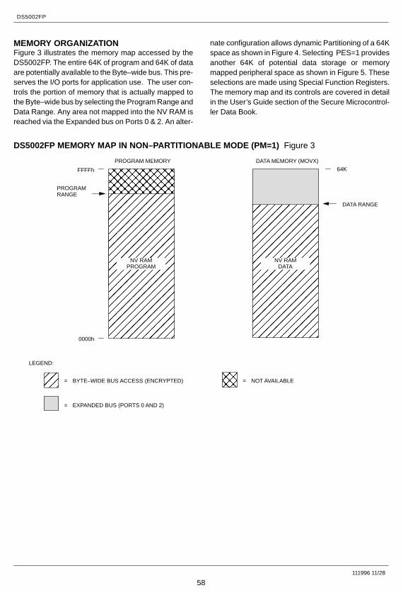
MEMORY ORGANIZATIONFigure 3 illustrates the memory map accessed by theDS5002FP. The entire 64K of program and 64K of dataare potentially available to the Byte–wide bus. This pre-serves the I/O ports for application use. The user con-trols the portion of memory that is actually mapped tothe Byte–wide bus by selecting the Program Range andData Range. Any area not mapped into the NV RAM isreached via the Expanded bus on Ports 0 & 2. An alter-
nate configuration allows dynamic Partitioning of a 64Kspace as shown in Figure 4. Selecting PES=1 providesanother 64K of potential data storage or memorymapped peripheral space as shown in Figure 5. Theseselections are made using Special Function Registers.The memory map and its controls are covered in detailin the User’s Guide section of the Secure Microcontrol-ler Data Book.
DS5002FP MEMORY MAP IN NON–PARTITIONABLE MODE (PM=1) Figure 3
ÎÎÎÎÎÎÎÎÎÎÎÎÎÎÎÎÎÎÎÎÎÎÎÎÎÎÎÎÎÎÎÎÎÎÎÎÎÎÎÎÎÎÎÎÎ
FFFFh
0000h
ÏÏÏÏ
= BYTE–WIDE BUS ACCESS (ENCRYPTED)
LEGEND:
ÏÏÏÏÏÏÏÏÏÏÏÏÏÏÏÏÏÏÏÏÏÏÏÏÏÏÏÏÏÏÏÏÏÏÏÏÏÏÏÏÏÏÏÏÏÏÏÏÏÏÏÏÏÏÏ
NV RAMPROGRAM
PROGRAM
=
ÎÎÎÎ
=
PROGRAM MEMORY
EXPANDED BUS (PORTS 0 AND 2)
NOT AVAILABLE
DATA MEMORY (MOVX)
ÏÏÏÏÏÏÏÏÏÏÏÏÏÏÏÏÏÏÏÏÏÏÏÏÏÏÏÏÏÏÏÏÏÏÏÏÏÏÏÏÏÏÏÏÏÏÏÏÏÏ
NV RAMDATA
64K
DATA RANGE
RANGE

DATA MEMORY (MOVX)
ÏÏÏÏÏÏÏÏÏÏÏÏÏÏÏÏÏÏÏÏÏÏÏÏÏÏÏÏÏÏÏÏÏÏÏÏÏÏÏÏ
ÎÎÎÎÎÎÎÎÎÎÎÎÎÎÎÎÎÎÎÎÎÎÎÎÎ
PROGRAM MEMORY
NV RAMPROGRAM
FFFFh
4000h
0000h
PARTITION
ÎÎÎÎÎÎ
NOT ACCESSIBLE
ÏÏÏÏÏÏ
BYTE–WIDE PROGRAM (ENCRYPTED)
LEGEND:
PE3
PE4
64K
48K
32K
16K
PE1
PE2
DS5002FP
111996 12/28
59
DS5002FP MEMORY MAP IN PARTITIONABLE MODE (PM=0) Figure 4
ÎÎÎÎÎÎÎÎÎÎÎÎÎÎÎÎÎÎÎÎÎÎÎÎÎÎÎÎÎÎÎÎÎÎÎÎÎÎÎÎÎÎÎÎÎ
FFFFh
0000h
ÉÉÉÉ
= NVRAM MEMORY
LEGEND:
ÉÉÉÉÉÉÉÉÉÉÉÉÉÉÉÉÉÉÉÉÉÉÉÉÉÉÉÉÉÉÉÉÉÉÉÉÉÉÉÉÉÉÉÉÉ
NV RAMDATA
ÉÉÉÉÉÉÉÉÉÉÉÉÉÉÉÉÉÉÉÉ
NV RAMPROGRAM
PARTITION
=
ÎÎÎÎ
=
PROGRAM MEMORY
EXPANDED BUS (PORTS 0 AND 2)
NOT AVAILABLE
DATA MEMORY (MOVX)
NOTE: Partitionable mode is not supported when MSEL=0 (128KB mode).
DS5002FP MEMORY MAP WITH PES=1 Figure 5

DS5002FP
111996 13/28
60
Figure 6 illustrates a typical memory connection for asystem using a 128K byte SRAM. Note that in this con-figuration, both program and data are stored in a com-mon RAM chip Figure 7 shows a similar system with
using two 32K byte SRAMs. The Byte–wide Addressbus connects to the SRAM address lines. The bi–direc-tional Byte–wide data bus connects the data I/O lines ofthe SRAM.
DS5002FP CONNECTION TO 128K X 8 SRAM Figure 6
ÌÌÌÌ
ÌÌÌÌÌÌÌÌÌÌÌÌÌÌÌÌÌÌ
ÑÑÑÑ
ÑÑÑÑÑÑÑÑÑÑÑÑÑÑÑÑÑÑÑÑÇ
ÇÇÇÇÇÇÇÇÇ
ÇÇ
ÇÇÇÇÇÇÇÇ
ÇÇ
ÇÇÇÇÇÇÇÇ
ÇÇ
ÇÇÇÇÇÇÇÇ
13
54
+3V
+5V 12
10
74
32
29
22
24
16
5214
128K x 8 SRAMDS5002FP
VCC
WE
CS1
A16
A14–A0
A15
D7–D0
GND
CS2
OE
VCCO
R/W
CE1
CE2
BA14–BA0
CE3
BD7–BD0
GND
VCC
VLI
PORT0
PORT1
PORT2
PORT3
MSEL
2
63
30
2
31
LITHIUM

DS5002FP
111996 14/28
61
DS5002FP CONNECTION TO 64K X 8 SRAM Figure 7
ÇÇÇÇÇÇÇÇÇÇÇÇ
ÇÇÇÇÇÇÇÇÇÇ
ÇÇÇÇÇÇÇÇÇÇÇÇ
ÇÇÇÇÇÇÇÇÇÇÇÇ
VCCO
R/W
CE1
CE2
BA14–BA0
BD7–BD0
GND
VCC
VLI
PORT0
PORT1
PORT2
PORT3
MSEL
28
27
20
14
32K x 8 SRAM
VCC
WE
CS
A14–A0
D7–D0
GND
OE
VCC
WE
CS
A14–A0
D7–D0
GND
OE
32K x 8SRAM
ÑÑÑÑÑÑÑÑÑÑÑÑÑÑÑÑÑÑÑÑÑÑÑÑÑÑÑÑÑÑÑÑÑÑÑÑÑÑÑÑÑÑÑÑÑÑÑÑÑÑÑÑÑÑÑÑÑÑÑÑÑÑÑÑÑÑÑÑÑÑÑÑÑÑÑÑÑÑÑÑÑÑÑÑÑÑÑÑÑÑÑÑÑÑÑÑÑÑÑÑÑÑÑÑÑÑÑÑÑÑÑÑÑÑÑÑÑÑÑÑÑÑÑÑÑÑÑÑÑÑÑÑÑÑÑÑÑÑÑÑ
ÓÓÓÓÓÓÓÓÓÓÓÓÓÓÓÓÓÓÓÓÓÓÓÓÓÓÓÓÓÓÓÓÓÓÓÓÓÓÓÓÓÓÓÓÓÓÓÓÓÓÓÓÓÓÓÓÓÓÓÓÓÓÓÓÓÓÓÓÓÓÓÓÓÓÓÓÓÓÓÓÓÓÓÓÓÓÓÓÓÓÓÓÓÓÓÓÓÓÓÓÓÓÓÓÓÓÓÓÓÓÓÓÓÓÓÓÓÓÓÓÓÓÓÓÓÓÓÓÓÓÓÓÓÓÓÓÓÓÓÓ
28
27
20
14
32K x 8 SRAM
VCC
WE
CS
A14–A0
D7–D0
GND
OE
22
22
52
12
10
74
13
54
+3V
+5V
DS5002FP
2
LITHIUM
14+5V
POWER MANAGEMENTThe DS5002FP monitors VCC to provide Power–failReset, early warning Power–fail Interrupt, and switchover to lithium backup. It uses an internal band–gap ref-erence in determining the switch points. These arecalled VPFW, VCCMIN, and VLI respectively. When VCCdrops below VPFW, the DS5002FP will perform an inter-rupt vector to location 2Bh if the power–fail warning wasenabled. Full processor operation continues regard-less. When power falls further to VCCMIN, theDS5002FP invokes a reset state. No further codeexecution will be performed unless power rises backabove VCCMIN. All decoded chip enables and the R/Wsignal go to an inactive (logic 1) state. VCC is still thepower source at this time. When VCC drops further to
below VLI, internal circuitry will switch to the lithium cellfor power. The majority of internal circuits will be dis-abled and the remaining nonvolatile states will beretained. Any devices connected to VCCO will be pow-ered by the lithium cell at this time. VCCO will be at thelithium battery voltage less a diode drop. This drop willvary depending on the load. Low power SRAMs shouldbe used for this reason. When using the DS5002FP, theuser must select the appropriate battery to match theRAM data retention current and the desired backup life-time. Note that the lithium cell is only loaded when VCC <VLI. The User’s Guide has more information on thistopic. The trip points VCCMIN and VPFW are listed in theelectrical specifications.

DS5002FP
111996 15/28
62
ELECTRICAL SPECIFICATIONSThe DS5002FP adheres to all AC and DC electricalspecifications published for the DS5001FP. The abso-
lute maximum ratings and unique specifications for theDS5002FP are listed below.
ABSOLUTE MAXIMUM RATINGS*Voltage on Any Pin Relative to Ground –0.3V to +7.0VOperating Temperature 0°C to 70°CStorage Temperature –40°C to +70°CSoldering Temperature 260°C for 10 seconds
* This is a stress rating only and functional operation of the device at these or any other conditions above thoseindicated in the operation sections of this specification is not implied. Exposure to absolute maximum ratingconditions for extended periods of time may affect reliability.
DC CHARACTERISTICS (tA = 0°C to 70°C; VCC=5V ± 10%)
PARAMETER SYMBOL MIN TYP MAX UNITS NOTES
Input Low Voltage VIL –0.3 +0.8 V 1
Input High Voltage VIH1 2.0 VCC+0.3 V 1
Input High Voltage (RST, XTAL1,PROG)
VIH2 3.5 VCC+0.3 V 1
Output Low Voltage@ IOL=1.6 mA (Ports 1, 2, 3)
VOL1 0.15 0.45 V 1
Output Low Voltage@ IOL=3.2 mA (Port 0, ALE, PF,BA15–0, BD7–0, R/W, CE1N,CE1–4, PE1–4, VRST)
VOL2 0.15 0.45 V 1
Output High Voltage@ IOH=–80 µA (Ports 1, 2, 3)
VOH1 2.4 4.8 V 1
Output High Voltage@ IOH=–400 µA (Ports 0, ALE,PF, BA15–0, BD7–0, R/W, CE1N,CE1–4, PE1–4)
VOH2 2.4 4.8 V 1
Input Low CurrentVIN=0.45V (Ports 1, 2, 3)
IIL –50 µA
Transition Current; 1 to 0VIN=2.0V (Ports 1, 2, 3)(0°C to 70°C)
ITL –500 µA
Transition Current; 1 to 0VIN=2.0V (Ports 1, 2, 3)(–40°C to +85°C)
ITL –600 µA 12
SDI Input Low Voltage VILS 0.4 V 1
SDI Input High Voltage VIHS 2.0 VCCO V 1, 11
SDI Pull–Down Resistor RSDI 25 60 KΩ
Battery–Backup Quiescent Current IBAT 5 75 nA 7

DS5002FP
111996 16/28
63
DC CHARACTERISTICS (cont’d) (tA = 0°C to 70°C; VCC=5V ± 10%)
PARAMETER SYMBOL MIN TYP MAX UNITS NOTES
Input Leakage Current0.45 < VIN < VCC (Port 0, MSEL)
IIL ±10 µA
RST Pull–down Resistor(0°C to 70°C)
RRE 40 150 KΩ
RST Pull–down Resistor(–40°C to +85°C)
RRE 40 180 KΩ 12
VRST Pull–up Resistor RVR 4.7 KΩ
PROG Pull–up Resistor RPR 40 KΩ
Power–Fail Warning Voltage(0°C to 70°C)
VPFW 4.25 4.37 4.50 V 1
Power–Fail Warning Voltage(–40°C to +85°C)
VPFW 4.1 4.37 4.5 V 1, 12
Minimum Operating Voltage(0°C to 70°C)
VCCMIN 4.00 4.12 4.25 V 1
Minimum Operating Voltage(–40°C to +85°C)
VCCMIN 3.85 4.09 4.25 V 1, 12
Lithium Supply Voltage VLI 2.5 4.0 V 1
Operating Current @ 16 MHz ICC 36 mA 2
Idle Mode Current @ 12 MHz(0°C to 70°C)
IIDLE 7.0 mA 3
Idle Mode Current @ 12 MHz(–40°C to +85°C)
IIDLE 8.0 mA 3, 12
Stop Mode Current ISTOP 80 µA 4
Pin Capacitance CIN 10 pF 5
Output Supply Voltage (VCCO) VCCO1 VCC–0.35 V 1, 2
Output Supply Battery–backedMode (VCCO, CE1–4, PE1–2)(0°C to 70°C)
VCCO2 VLI–0.65 V 1, 8
Output Supply Battery–backedMode (VCCO, CE1–4, PE1–2)(–40°C to +85°C)
VCCO2 VLI–0.9 V 1, 8, 12
Output Supply Current@ VCCO=VCC – 0.3V
ICCO1 75 mA 6
Lithium–backed Quiescent Current ILI 5 75 nA 7
Reset Trip Point in Stop Modew/BAT=3.0V (0°C to 70°C)w/BAT=3.0V (–40°C to +85°C)w/BAT=3.3V (0°C to 70°C)
4.03.854.4
4.254.254.65
11, 12
1

DS5002FP
111996 17/28
64
AC CHARACTERISTICS (tA = 0°C to70°C; VCC=0V to 5V)
PARAMETER SYMBOL MIN TYP MAX UNITS NOTES
SDI Pulse Reject tSPR 2 µs 10
SDI Pulse Accept tSPA 10 µs 10
AC CHARACTERISTICSEXPANDED BUS MODE TIMING SPECIFICATIONS (tA = 0°C to70°C; VCC=5V + 10%)
# PARAMETER SYMBOL MIN MAX UNITS
1 Oscillator Frequency 1/tCLK 1.0 16 MHz
2 ALE Pulse Width tALPW 2tCLK–40 ns
3 Address Valid to ALE Low tAVALL tCLK–40 ns
4 Address Hold After ALE Low tAVAAV tCLK–35 ns
14 RD Pulse Width tRDPW 6tCLK–100 ns
15 WR Pulse Width tWRPW 6tCLK–100 ns
16 RD Low to Valid Data In @12 MHz @16 MHz tRDLDV
5tCLK–1655tCLK–105
nsns
17 Data Hold after RD High tRDHDV 0 ns
18 Data Float after RD High tRDHDZ 2tCLK–70 ns
19 ALE Low to Valid Data In @12 MHz @16 MHz tALLVD
8tCLK–1508tCLK–90
nsns
20 Valid Addr. to Valid Data In @12 MHz @16 MHz tAVDV
9tCLK–1659tCLK–105
nsns
21 ALE Low to RD or WR Low tALLRDL 3tCLK–50 3tCLK+50 ns
22 Address Valid to RD or WR Low tAVRDL 4tCLK–130 ns
23 Data Valid to WR Going Low tDVWRL tCLK–60 ns
24 Data Valid to WR High @12 MHz @16 MHz tDVWRH
7tCLK–1507tCLK–90
nsns
25 Data Valid after WR High tWRHDV tCLK–50 ns
26 RD Low to Address Float tRDLAZ 0 ns
27 RD or WR High to ALE High tRDHALH tCLK–40 tCLK+50 ns

DS5002FP
111996 18/28
65
EXPANDED DATA MEMORY READ CYCLE
27
19
21 14
16
264
3
22
20
17
18
ALE
PORT 0
PORT 2 P2.7–P2.0 OR A15–A8 FROM DPH A15–A8 FROM PCH
DATA IN INSTRIN
A7–A0(PCL)
A7–A0(Rn OR DPL)
RD
2
EXPANDED DATA MEMORY WRITE CYCLE
27
21
15
23
3 4 24
25
22
ALE
PORT 0
PORT 2
WR
DATA OUTA7–A0
(Rn OR DPL)A7–A0(PCL)
INSTRIN
P2.7–P2.0 OR A15–A8 FROM PDH A15–A8 FROM PCH
DS5002FP
111996 19/28
66
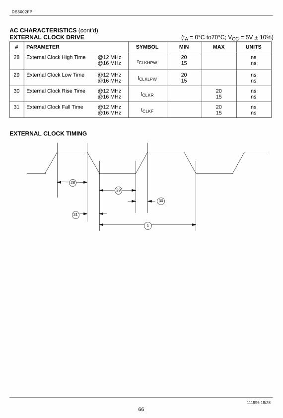
AC CHARACTERISTICS (cont’d)EXTERNAL CLOCK DRIVE (tA = 0°C to70°C; VCC = 5V + 10%)
# PARAMETER SYMBOL MIN MAX UNITS
28 External Clock High Time @12 MHz @16 MHz tCLKHPW
2015
nsns
29 External Clock Low Time @12 MHz @16 MHz tCLKLPW
2015
nsns
30 External Clock Rise Time @12 MHz @16 MHz tCLKR
2015
nsns
31 External Clock Fall Time @12 MHz @16 MHz tCLKF
2015
nsns
EXTERNAL CLOCK TIMING
28
29
30
31
1

DS5002FP
111996 20/28
67
AC CHARACTERISTICS (cont’d)POWER CYCLING TIMING (tA = 0°C to70°C; VCC = 5V + 10%)
# PARAMETER SYMBOL MIN MAX UNITS
32 Slew Rate from VCCmin to VLI tF 130 µs
33 Crystal Start up Time tCSU (note 9)
34 Power On Reset Delay tPOR 21504 tCLK
POWER CYCLE TIMING
VCCVPFW
VCCMIN
VLI
INTERRUPTSERVICEROUTINE
CLOCKOSC
INTERNALRESET
LITHIUMCURRENT
32
33
34

DS5002FP
111996 21/28
68
AC CHARACTERISTICS (cont’d)SERIAL PORT TIMING – MODE 0 (tA = 0°C to70°C; VCC = 5V + 10%)
# PARAMETER SYMBOL MIN MAX UNITS
35 Serial Port Clock Cycle Time tSPCLK 12tCLK µs
36 Output Data Setup to Rising Clock Edge tDOCH 10tCLK–133 ns
37 Output Data Hold after Rising Clock Edge tCHDO 2tCLK–117 ns
38 Clock Rising Edge to Input Data Valid tCHDV 10tCLK–133 ns
39 Input Data Hold after Rising Clock Edge tCHDIV 0 ns
SERIAL PORT TIMING – MODE 0
0 1 2 3 4 5 6 7 8
ALE
CLOCK
DATA OUT
INPUT DATA
0 1 2 3 4 5 6 7
35
37
36
3938
SET TI
SET RI
VALID VALIDVALIDVALIDVALIDVALIDVALID
CLEAR RI
WRITE TOSBUF REGISTER

DS5002FP
111996 22/28
69
AC CHARACTERISTICSBYTEWIDE ADDRESS/DATA BUS TIMING (tA = 0°C to70°C; VCC = 5V + 10%)
# PARAMETER SYMBOL MIN MAX UNITS
40 Delay to Byte–wide Address Valid fromCE1, CE2 or CE1N Low During OpcodeFetch
tCE1LPA 30 ns
41 Pulse Width of CE1–4, PE1–4 or CE1N tCEPW 4tCLK–35 ns
42 Byte–wide Address Hold After CE1, CE2or CE1N High During Opcode Fetch
tCE1HPA 2tCLK–20 ns
43 Byte–wide Data Setup to CE1, CE2 orCE1N High During Opcode Fetch
tOVCE1H 1tCLK+40 ns
44 Byte–wide Data Hold After CE1, CE2 orCE1N High During Opcode Fetch
tCE1HOV 10 ns
45 Byte–wide Address Hold After CE1–4,PE1–4, or CE1N High During MOVX
tCEHDA 4tCLK–30 ns
46 Delay from Bytewide Address ValidCE1–4, PE1–4, or CE1N Low DuringMOVX
tCELDA 4tCLK–35 ns
47 Byte–wide Data Setup to CE1–4, PE1–4,or CE1N High During MOVX (read)
tDACEH 1tCLK+40 ns
48 Byte–wide Data Hold After CE1–4,PE1–4, or CE1N High During MOVX(read)
tCEHDV 10 ns
49 Byte–wide Address Valid to R/W ActiveDuring MOVX (write)
tAVRWL 3tCLK–35 ns
50 Delay from R/W Low to Valid Data OutDuring MOVX (write)
tRWLDV 20 ns
51 Valid Data Out Hold Time from CE1–4,PE1–4, or CE1N High
tCEHDV 1tCLK–15 ns
52 Valid Data Out Hold Time from R/W High tRWHDV 0 ns
53 Write Pulse Width (R/W Low Time) tRWLPW 6tCLK–20 ns

DS5002FP
111996 23/28
70
BYTEWIDE BUS TIMING
RPC AC CHARACTERISTICS – DBB READ (tA = 0°C to70°C; VCC = 5V + 10%)
# PARAMETER SYMBOL MIN MAX UNITS
54 CS, A0 Setup to RD tAR 0 ns
55 CS, A0 Hold After RD tRA 0 ns
56 RD Pulse Width tRR 160 ns
57 CS, A0 to Data Out Delay tAD 130 ns
58 RD to Data Out Delay tRD 0 130 ns
59 RD to Data Float Delay tRDZ 85 ns

DS5002FP
111996 24/28
71
RPC AC CHARACTERISTICS – DBB WRITE (tA = 0°C to70°C; VCC = 5V + 10%)
# PARAMETER SYMBOL MIN MAX UNITS
60 CS, A0 Setup to WR tAW 0 ns
61A CS, Hold After WR tWA 0 ns
61B A0, Hold After WR tWA 20 ns
62 WR Pulse Width tWW 160 ns
63 Data Setup to WR tDW 130 ns
64 Data Hold After WR tWD 20 ns
AC CHARACTERISTICS – DMA (tA = 0°C to70°C; VCC = 5V + 10%)
# PARAMETER SYMBOL MIN MAX UNITS
65 DACK to WR or RD tACC 0 ns
66 RD or WR to DACK tCAC 0 ns
67 DACK to Data Valid tACD 0 130 ns
68 RD or WR to DRQ Cleared tCRQ 110 ns
AC CHARACTERISTICS – PROG (tA = 0°C to70°C; VCC = 5V + 10%)
# PARAMETER SYMBOL MIN MAX UNITS
69 PROG Low to Active tPRA 48 CLKS
70 PROG High to Inactive tPRI 48 CLKS

DS5002FP
111996 25/28
72
RPC TIMING MODE
CS OR A0
RD
DATA
CS OR A0
WR
DATA
READ OPERATION
WRITE OPERATION
DATA VALID
DATA VALID
DACK
RD
WR
DATA
DRQ
DMA
VALID VALID
5456
57
58 59
55
626160
63 64
65 66
67
65 66
68 68

DS5002FP
111996 26/28
73
NOTES:All parameters apply to both commercial and industrial temperature operation unless otherwise noted.
1. All voltages are referenced to ground.
2. Maximum operating ICC is measured with all output pins disconnected; XTAL1 driven with tCLKR, tCLKF=10 ns, VIL = 0.5V; XTAL2 disconnected; RST = PORT0 = VCC, MSEL = VSS.
3. Idle mode IIDLE is measured with all output pins disconnected; XTAL1 driven with tCLKR, tCLKF = 10 ns, VIL = 0.5V; XTAL2 disconnected; PORT0 = VCC, RST = MSEL = VSS.
4. Stop mode ISTOP is measured with all output pins disconnected; PORT0 = VCC; XTAL2 not connected;RST = MSEL = XTAL1 = VSS.
5. Pin Capacitance is measured with a test frequency – 1 MHz, tA = 25°C.
6. ICCO1 is the maximum average operating current that can be drawn from VCCO in normal operation.
7. ILI is the current drawn from VLI input when VCC = 0V and VCCO is disconnected. Battery–backed mode:2.5V < VBAT < 4.0; VCC < VBAT; VSDI should be < VILS for IBAT max.
8. VCCO2 is measured with VCC < VLI, and a maximum load of 10 µA on VCCO.
9. Crystal start–up time is the time required to get the mass of the crystal into vibrational motion from the timethat power is first applied to the circuit until the first clock pulse is produced by the on–chip oscillator. Theuser should check with the crystal vendor for a worst case specification on this time.
10. SDI is deglitched to prevent accidental destruction. The pulse must be longer than tSPR to pass the deglitch-er, but SDI is not guaranteed unless it is longer than tSPA.
11. VIHS minimum is 2.0V or VCCO, whichever is lower.
12. This parameter applies to industrial temperature operation.
DS5002FP
111996 27/28
74
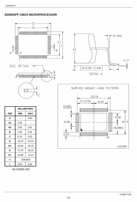
DS5002FP CMOS MICROPROCESSOR
DIM
MILLIMETERS
DIM MIN MAX
A – 3.40
A1 0.25 –
A2 2.55 2.87
B 0.30 0.50
C 0.13 0.23
D 23.70 24.10
D1 19.90 20.10
E 17.70 18.10
E1 13.90 14.10
e 0.80 BSC
L 0.65 0.95
56–G4005–001

DS5002FP
111996 28/28
75
DATA SHEET REVISION SUMMARYThe following represent the key differences between 11/27/95 and 07/30/96 version of the DS5002FP data sheet.Please review this summary carefully.
1. Change VCC02 specification from VLI –0.5 to VLI –0.65 (PCN F62501).
2. Update mechanical specifications.
The following represent the key differences between 07/30/96 and 11/19/96 version of the DS5002FP data sheet.Please review this summary carefully.
1. Change VCC01 from VCC–0.3 to VCC–0.35.