Embed Size (px)
Citation preview
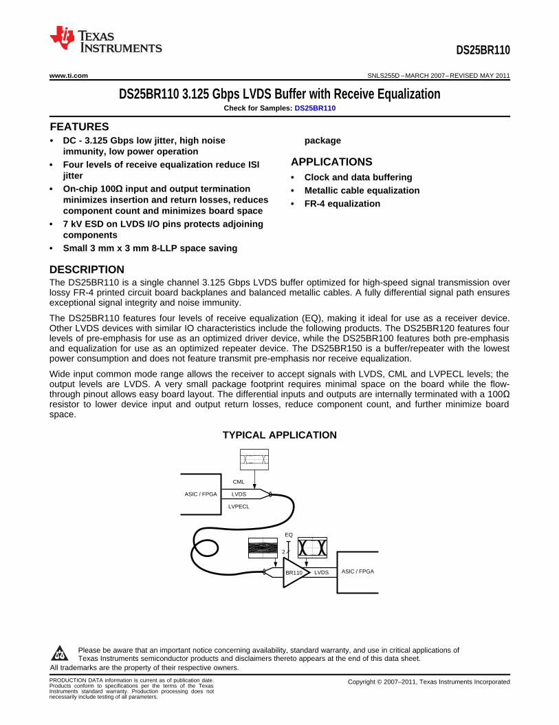
ASIC / FPGA
EQ
CML
LVDS
LVPECL
ASIC / FPGALVDS
2
BR110
DS25BR110
www.ti.com SNLS255D –MARCH 2007–REVISED MAY 2011
DS25BR110 3.125 Gbps LVDS Buffer with Receive EqualizationCheck for Samples: DS25BR110
1FEATURES2• DC - 3.125 Gbps low jitter, high noise package
immunity, low power operationAPPLICATIONS• Four levels of receive equalization reduce ISI
jitter • Clock and data buffering• On-chip 100Ω input and output termination • Metallic cable equalization
minimizes insertion and return losses, reduces • FR-4 equalizationcomponent count and minimizes board space
• 7 kV ESD on LVDS I/O pins protects adjoiningcomponents
• Small 3 mm x 3 mm 8-LLP space saving
DESCRIPTIONThe DS25BR110 is a single channel 3.125 Gbps LVDS buffer optimized for high-speed signal transmission overlossy FR-4 printed circuit board backplanes and balanced metallic cables. A fully differential signal path ensuresexceptional signal integrity and noise immunity.
The DS25BR110 features four levels of receive equalization (EQ), making it ideal for use as a receiver device.Other LVDS devices with similar IO characteristics include the following products. The DS25BR120 features fourlevels of pre-emphasis for use as an optimized driver device, while the DS25BR100 features both pre-emphasisand equalization for use as an optimized repeater device. The DS25BR150 is a buffer/repeater with the lowestpower consumption and does not feature transmit pre-emphasis nor receive equalization.
Wide input common mode range allows the receiver to accept signals with LVDS, CML and LVPECL levels; theoutput levels are LVDS. A very small package footprint requires minimal space on the board while the flow-through pinout allows easy board layout. The differential inputs and outputs are internally terminated with a 100Ωresistor to lower device input and output return losses, reduce component count, and further minimize boardspace.
TYPICAL APPLICATION
1
Please be aware that an important notice concerning availability, standard warranty, and use in critical applications ofTexas Instruments semiconductor products and disclaimers thereto appears at the end of this data sheet.
2All trademarks are the property of their respective owners.
PRODUCTION DATA information is current as of publication date. Copyright © 2007–2011, Texas Instruments IncorporatedProducts conform to specifications per the terms of the TexasInstruments standard warranty. Production processing does notnecessarily include testing of all parameters.
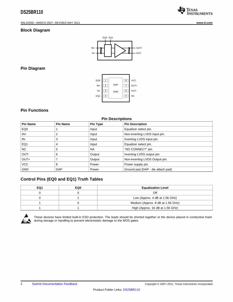
EQ0
IN+
IN-
EQ1
VCC
OUT+
OUT-
NC
1
2
3
4
8
6
5
7
GND
DAP
OUT+
OUT-
EQ0
IN+
IN-
EQ1
DS25BR110
SNLS255D –MARCH 2007–REVISED MAY 2011 www.ti.com
Block Diagram
Pin Diagram
Pin Functions
Pin DescriptionsPin Name Pin Name Pin Type Pin Description
EQ0 1 Input Equalizer select pin.
IN+ 2 Input Non-inverting LVDS input pin.
IN- 3 Input Inverting LVDS input pin.
EQ1 4 Input Equalizer select pin.
NC 5 NA "NO CONNECT" pin.
OUT- 6 Output Inverting LVDS output pin.
OUT+ 7 Output Non-inverting LVDS Output pin.
VCC 8 Power Power supply pin.
GND DAP Power Ground pad (DAP - die attach pad)
Control Pins (EQ0 and EQ1) Truth Tables
EQ1 EQ0 Equalization Level
0 0 Off
0 1 Low (Approx. 4 dB at 1.56 GHz)
1 0 Medium (Approx. 8 dB at 1.56 GHz)
1 1 High (Approx. 16 dB at 1.56 GHz)
These devices have limited built-in ESD protection. The leads should be shorted together or the device placed in conductive foamduring storage or handling to prevent electrostatic damage to the MOS gates.
2 Submit Documentation Feedback Copyright © 2007–2011, Texas Instruments Incorporated
Product Folder Links: DS25BR110
DS25BR110
www.ti.com SNLS255D –MARCH 2007–REVISED MAY 2011
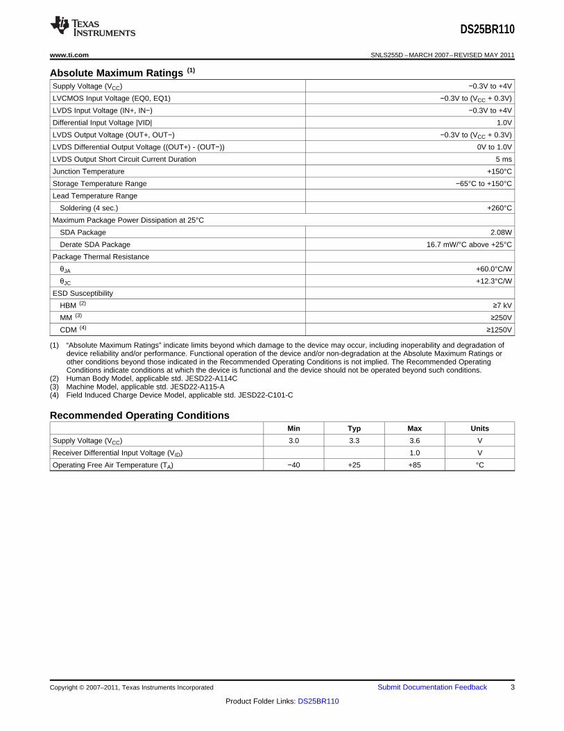
Absolute Maximum Ratings (1)
Supply Voltage (VCC) −0.3V to +4V
LVCMOS Input Voltage (EQ0, EQ1) −0.3V to (VCC + 0.3V)
LVDS Input Voltage (IN+, IN−) −0.3V to +4V
Differential Input Voltage |VID| 1.0V
LVDS Output Voltage (OUT+, OUT−) −0.3V to (VCC + 0.3V)
LVDS Differential Output Voltage ((OUT+) - (OUT−)) 0V to 1.0V
LVDS Output Short Circuit Current Duration 5 ms
Junction Temperature +150°C
Storage Temperature Range −65°C to +150°C
Lead Temperature Range
Soldering (4 sec.) +260°C
Maximum Package Power Dissipation at 25°C
SDA Package 2.08W
Derate SDA Package 16.7 mW/°C above +25°C
Package Thermal Resistance
θJA +60.0°C/W
θJC +12.3°C/W
ESD Susceptibility
HBM (2) ≥7 kV
MM (3) ≥250V
CDM (4) ≥1250V
(1) “Absolute Maximum Ratings” indicate limits beyond which damage to the device may occur, including inoperability and degradation ofdevice reliability and/or performance. Functional operation of the device and/or non-degradation at the Absolute Maximum Ratings orother conditions beyond those indicated in the Recommended Operating Conditions is not implied. The Recommended OperatingConditions indicate conditions at which the device is functional and the device should not be operated beyond such conditions.
(2) Human Body Model, applicable std. JESD22-A114C(3) Machine Model, applicable std. JESD22-A115-A(4) Field Induced Charge Device Model, applicable std. JESD22-C101-C
Recommended Operating ConditionsMin Typ Max Units
Supply Voltage (VCC) 3.0 3.3 3.6 V
Receiver Differential Input Voltage (VID) 1.0 V
Operating Free Air Temperature (TA) −40 +25 +85 °C
Copyright © 2007–2011, Texas Instruments Incorporated Submit Documentation Feedback 3
Product Folder Links: DS25BR110

DS25BR110
SNLS255D –MARCH 2007–REVISED MAY 2011 www.ti.com
DC Electrical CharacteristicsOver recommended operating supply and temperature ranges unless otherwise specified. (1) (2) (3)
Symbol Parameter Conditions Min Typ Max Units
LVCMOS INPUT DC SPECIFICATIONS (EQ0, EQ1)
VIH High Level Input Voltage 2.0 VCC V
VIL Low Level Input Voltage GND 0.8 V
IIH High Level Input Current VIN = 3.6V 0 ±10 μAVCC = 3.6V
IIL Low Level Input Current VIN = GND 0 ±10 μAVCC = 3.6V
VCL Input Clamp Voltage ICL = −18 mA, VCC = 0V -0.9 −1.5 V
LVDS OUTPUT DC SPECIFICATIONS (OUT+, OUT-)
VOD Differential Output Voltage 250 350 450 mVRL = 100ΩΔVOD Change in Magnitude of VOD for Complimentary -35 35 mVOutput States
VOS Offset Voltage 1.05 1.2 1.375 VRL = 100ΩΔVOS Change in Magnitude of VOS for Complimentary -35 35 mVOutput States
IOS Output Short Circuit Current (4) OUT to GND -35 -55 mA
OUT to VCC 7 55 mA
COUT Output Capacitance Any LVDS Output Pin to GND 1.2 pF
ROUT Output Termination Resistor Between OUT+ and OUT- 100 ΩLVDS INPUT DC SPECIFICATIONS (IN+, IN-)
VID Input Differential Voltage 0 1 V
VTH Differential Input High Threshold VCM = +0.05V or VCC-0.05V 0 +100 mV
VTL Differential Input Low Threshold −100 0 mV
VCMR Common Mode Voltage Range VID = 100 mV 0.05 VCC - V0.05
VIN = 3.6V or 0V ±1 ±10 μAIIN Input Current VCC = 3.6V or 0V
CIN Input Capacitance Any LVDS Input Pin to GND 1.7 pF
RIN Input Termination Resistor Between IN+ and IN- 100 ΩSUPPLY CURRENT
ICC Supply Current EQ0 = 0, EQ1 = 0 35 43 mA
(1) The Electrical Characteristics tables list guaranteed specifications under the listed Recommended Operating Conditions except asotherwise modified or specified by the Electrical Characteristics Conditions and/or Notes. Typical specifications are estimations only andare not guaranteed.
(2) Current into device pins is defined as positive. Current out of device pins is defined as negative. All voltages are referenced to groundexcept VOD and ΔVOD.
(3) Typical values represent most likely parametric norms for VCC = +3.3V and TA = +25°C, and at the Recommended Operation Conditionsat the time of product characterization and are not guaranteed.
(4) Output short circuit current (IOS) is specified as magnitude only, minus sign indicates direction only.
4 Submit Documentation Feedback Copyright © 2007–2011, Texas Instruments Incorporated
Product Folder Links: DS25BR110
DS25BR110
www.ti.com SNLS255D –MARCH 2007–REVISED MAY 2011
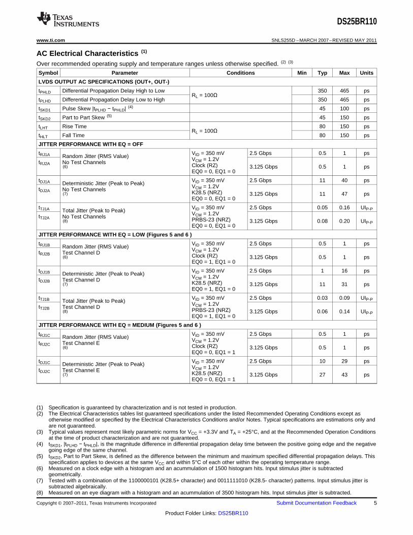
AC Electrical Characteristics (1)
Over recommended operating supply and temperature ranges unless otherwise specified. (2) (3)
Symbol Parameter Conditions Min Typ Max Units
LVDS OUTPUT AC SPECIFICATIONS (OUT+, OUT-)
tPHLD Differential Propagation Delay High to Low 350 465 psRL = 100Ω
tPLHD Differential Propagation Delay Low to High 350 465 ps
tSKD1 Pulse Skew |tPLHD − tPHLD| (4) 45 100 ps
tSKD2 Part to Part Skew (5) 45 150 ps
tLHT Rise Time 80 150 psRL = 100Ω
tHLT Fall Time 80 150 ps
JITTER PERFORMANCE WITH EQ = OFF
tRJ1A VID = 350 mV 2.5 Gbps 0.5 1 psRandom Jitter (RMS Value) VCM = 1.2VtRJ2A No Test Channels Clock (RZ) 3.125 Gbps 0.5 1 ps(6)EQ0 = 0, EQ1 = 0
tDJ1A VID = 350 mV 2.5 Gbps 11 40 psDeterministic Jitter (Peak to Peak) VCM = 1.2VtDJ2A No Test Channels K28.5 (NRZ) 3.125 Gbps 11 47 ps(7)EQ0 = 0, EQ1 = 0
tTJ1A VID = 350 mV 2.5 Gbps 0.05 0.16 UIP-PTotal Jitter (Peak to Peak) VCM = 1.2VtTJ2A No Test Channels PRBS-23 (NRZ) 3.125 Gbps 0.08 0.20 UIP-P(8)EQ0 = 0, EQ1 = 0
JITTER PERFORMANCE WITH EQ = LOW (Figures 5 and 6 )
tRJ1B VID = 350 mV 2.5 Gbps 0.5 1 psRandom Jitter (RMS Value) VCM = 1.2VtRJ2B Test Channel D Clock (RZ) 3.125 Gbps 0.5 1 ps(6)EQ0 = 1, EQ1 = 0
tDJ1B VID = 350 mV 2.5 Gbps 1 16 psDeterministic Jitter (Peak to Peak) VCM = 1.2VtDJ2B Test Channel D K28.5 (NRZ) 3.125 Gbps 11 31 ps(7)EQ0 = 1, EQ1 = 0
tTJ1B VID = 350 mV 2.5 Gbps 0.03 0.09 UIP-PTotal Jitter (Peak to Peak) VCM = 1.2VtTJ2B Test Channel D PRBS-23 (NRZ) 3.125 Gbps 0.06 0.14 UIP-P(8)EQ0 = 1, EQ1 = 0
JITTER PERFORMANCE WITH EQ = MEDIUM (Figures 5 and 6 )
tRJ1C VID = 350 mV 2.5 Gbps 0.5 1 psRandom Jitter (RMS Value) VCM = 1.2VtRJ2C Test Channel E Clock (RZ) 3.125 Gbps 0.5 1 ps(6)EQ0 = 0, EQ1 = 1
tDJ1C VID = 350 mV 2.5 Gbps 10 29 psDeterministic Jitter (Peak to Peak) VCM = 1.2VtDJ2C Test Channel E K28.5 (NRZ) 3.125 Gbps 27 43 ps(7)EQ0 = 0, EQ1 = 1
(1) Specification is guaranteed by characterization and is not tested in production.(2) The Electrical Characteristics tables list guaranteed specifications under the listed Recommended Operating Conditions except as
otherwise modified or specified by the Electrical Characteristics Conditions and/or Notes. Typical specifications are estimations only andare not guaranteed.
(3) Typical values represent most likely parametric norms for VCC = +3.3V and TA = +25°C, and at the Recommended Operation Conditionsat the time of product characterization and are not guaranteed.
(4) tSKD1, |tPLHD − tPHLD|, is the magnitude difference in differential propagation delay time between the positive going edge and the negativegoing edge of the same channel.
(5) tSKD2, Part to Part Skew, is defined as the difference between the minimum and maximum specified differential propagation delays. Thisspecification applies to devices at the same VCC and within 5°C of each other within the operating temperature range.
(6) Measured on a clock edge with a histogram and an acummulation of 1500 histogram hits. Input stimulus jitter is subtractedgeometrically.
(7) Tested with a combination of the 1100000101 (K28.5+ character) and 0011111010 (K28.5- character) patterns. Input stimulus jitter issubtracted algebraically.
(8) Measured on an eye diagram with a histogram and an acummulation of 3500 histogram hits. Input stimulus jitter is subtracted.
Copyright © 2007–2011, Texas Instruments Incorporated Submit Documentation Feedback 5
Product Folder Links: DS25BR110
DS25BR110
SNLS255D –MARCH 2007–REVISED MAY 2011 www.ti.com
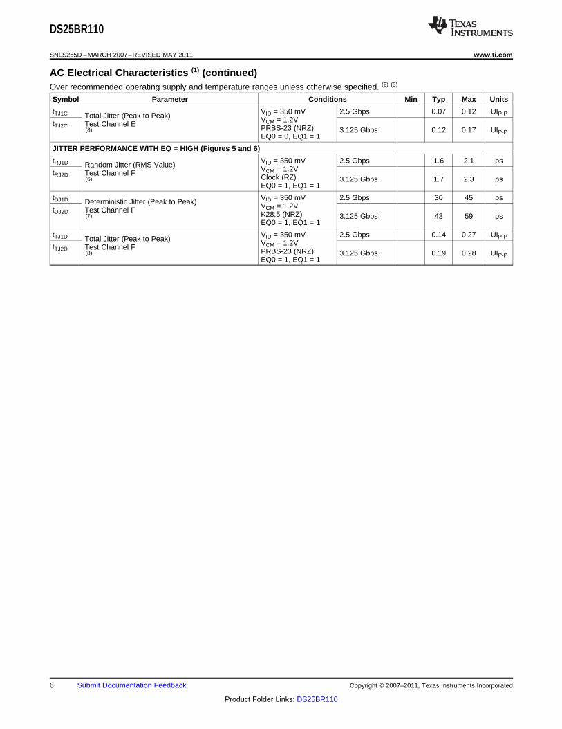
AC Electrical Characteristics (1) (continued)Over recommended operating supply and temperature ranges unless otherwise specified. (2) (3)
Symbol Parameter Conditions Min Typ Max Units
tTJ1C VID = 350 mV 2.5 Gbps 0.07 0.12 UIP-PTotal Jitter (Peak to Peak) VCM = 1.2VtTJ2C Test Channel E PRBS-23 (NRZ) 3.125 Gbps 0.12 0.17 UIP-P(8)EQ0 = 0, EQ1 = 1
JITTER PERFORMANCE WITH EQ = HIGH (Figures 5 and 6)
tRJ1D VID = 350 mV 2.5 Gbps 1.6 2.1 psRandom Jitter (RMS Value) VCM = 1.2VtRJ2D Test Channel F Clock (RZ) 3.125 Gbps 1.7 2.3 ps(6)EQ0 = 1, EQ1 = 1
tDJ1D VID = 350 mV 2.5 Gbps 30 45 psDeterministic Jitter (Peak to Peak) VCM = 1.2VtDJ2D Test Channel F K28.5 (NRZ) 3.125 Gbps 43 59 ps(7)EQ0 = 1, EQ1 = 1
tTJ1D VID = 350 mV 2.5 Gbps 0.14 0.27 UIP-PTotal Jitter (Peak to Peak) VCM = 1.2VtTJ2D Test Channel F PRBS-23 (NRZ) 3.125 Gbps 0.19 0.28 UIP-P(8)EQ0 = 1, EQ1 = 1
6 Submit Documentation Feedback Copyright © 2007–2011, Texas Instruments Incorporated
Product Folder Links: DS25BR110
L=1" L=1"
L=1"L=1"
L = A, B or C
100: DifferentialStripline
50: Microstrip
50: Microstrip
50: Microstrip
50: Microstrip
50: Microstrip
L=4"
L=4"
L=4"
L=4"
TEST CHANNEL
CHARACTERIZATION BOARD
DS25BR110
PATTERN GENERATOR
OSCILLOSCOPE
50: Microstrip
50: Microstrip
50: Microstrip
RL
OUT+
OUT-
IN+
IN-
Signal Generator R D
R D RL
VOL
OUT+
OUT-
IN+
IN-
Power Supply
Power Supply
VOH
DS25BR110
www.ti.com SNLS255D –MARCH 2007–REVISED MAY 2011
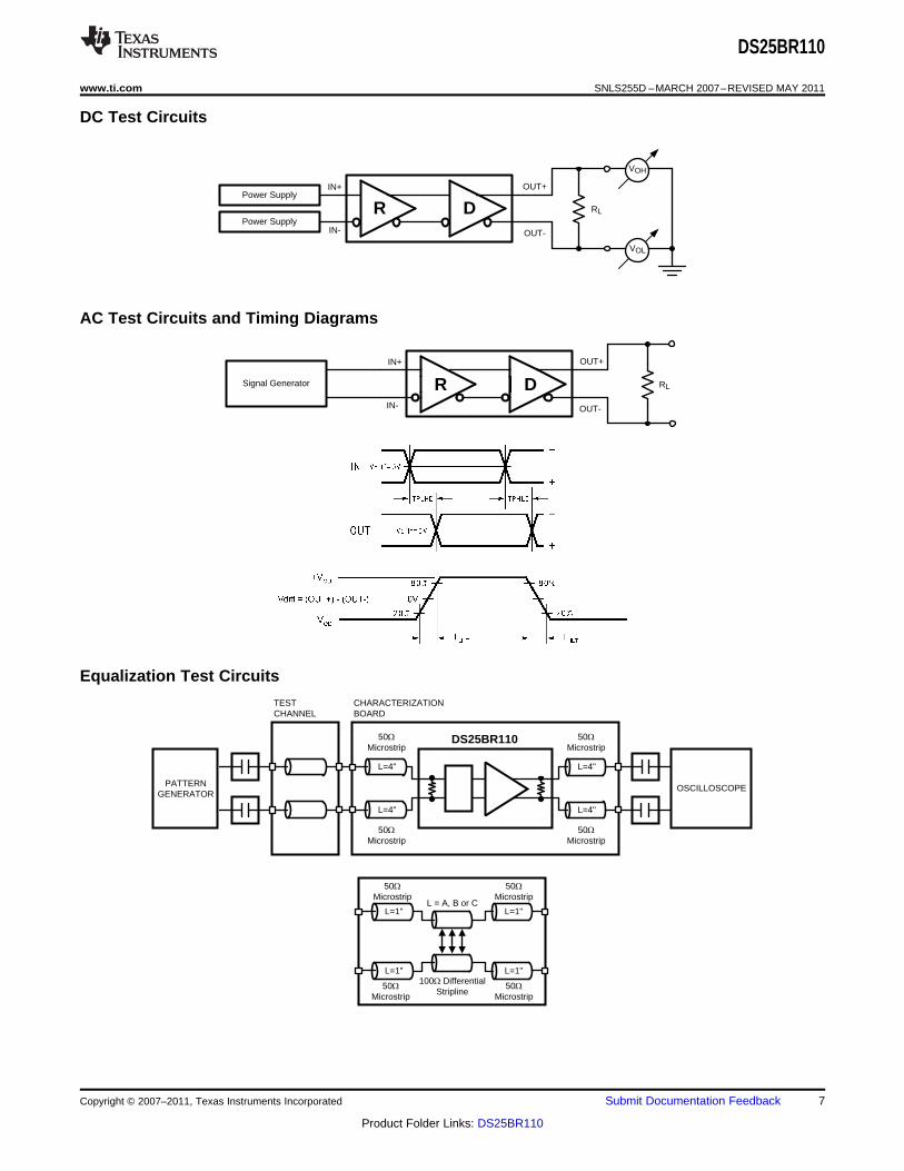
DC Test Circuits
AC Test Circuits and Timing Diagrams
Equalization Test Circuits
Copyright © 2007–2011, Texas Instruments Incorporated Submit Documentation Feedback 7
Product Folder Links: DS25BR110
OUT+
OUT-
DS25BR110
IN+
IN-
50:50:
VCC
CML3.3V or CML2.5V
100: Differential T-Line
OUT+
OUT-
DS25BR110
IN+
IN-
100: Differential T-Line
LVDS
DS25BR110
SNLS255D –MARCH 2007–REVISED MAY 2011 www.ti.com
Test Channel Loss Characteristics
The test channel was fabricated with Polyclad PCL-FR-370-Laminate/PCL-FRP-370 Prepreg materials (Dielectricconstant of 3.7 and Loss Tangent of 0.02). The edge coupled differential striplines have the following geometries:Trace Width (W) = 5 mils, Gap (S) = 5 mils, Height (B) = 16 mils.
Test Channel Length Insertion Loss (dB)(inches) 500 MHz 750 MHz 1000 MHz 1250 MHz 1500 MHz 1560 MHz
A 10 -1.2 -1.7 -2.0 -2.4 -2.7 -2.8
B 20 -2.6 -3.5 -4.1 -4.8 -5.5 -5.6
C 30 -4.3 -5.7 -7.0 -8.2 -9.4 -9.7
D 15 -1.6 -2.2 -2.7 -3.2 -3.7 -3.8
E 30 -3.4 -4.5 -5.6 -6.6 -7.7 -7.9
F 60 -7.8 -10.3 -12.4 -14.5 -16.6 -17.0
Device Operation
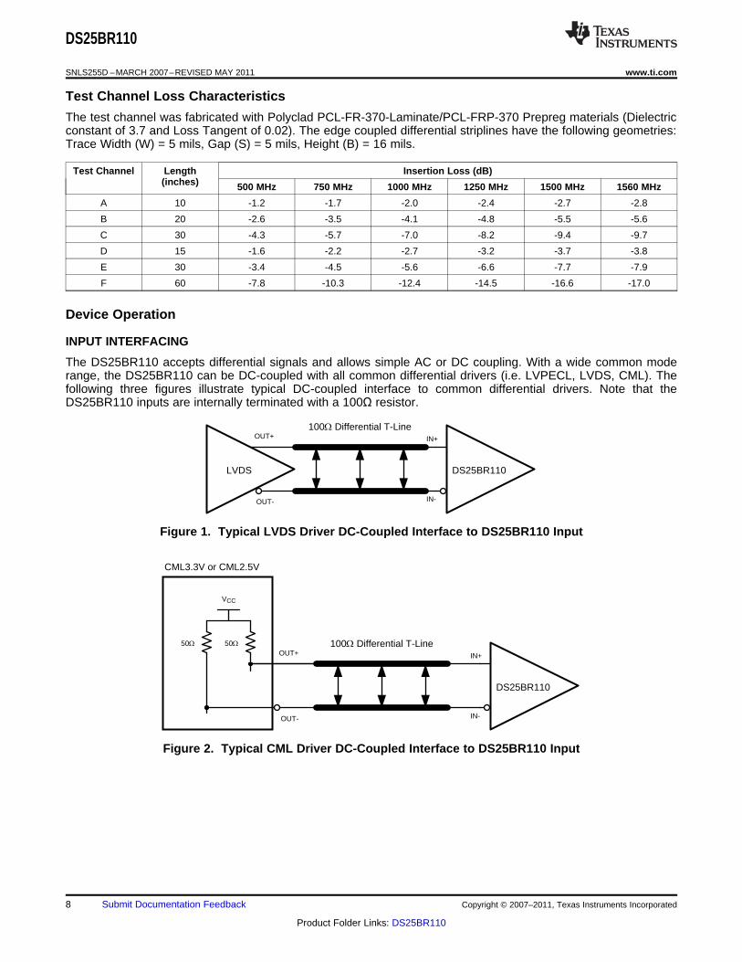
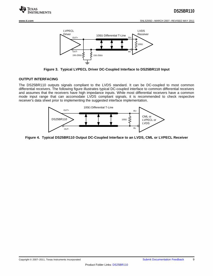
INPUT INTERFACING
The DS25BR110 accepts differential signals and allows simple AC or DC coupling. With a wide common moderange, the DS25BR110 can be DC-coupled with all common differential drivers (i.e. LVPECL, LVDS, CML). Thefollowing three figures illustrate typical DC-coupled interface to common differential drivers. Note that theDS25BR110 inputs are internally terminated with a 100Ω resistor.
Figure 1. Typical LVDS Driver DC-Coupled Interface to DS25BR110 Input
Figure 2. Typical CML Driver DC-Coupled Interface to DS25BR110 Input
8 Submit Documentation Feedback Copyright © 2007–2011, Texas Instruments Incorporated
Product Folder Links: DS25BR110
OUT+
OUT-
CML or LVPECL or LVDS
IN+
IN-
100:
100: Differential T-Line
DS25BR110
OUT+
OUT-
150-250:
100: Differential T-Line
LVDS Receiver
IN+
IN-
100:
LVPECL Driver
150-250:
DS25BR110
www.ti.com SNLS255D –MARCH 2007–REVISED MAY 2011
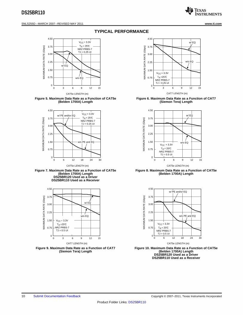
Figure 3. Typical LVPECL Driver DC-Coupled Interface to DS25BR110 Input
OUTPUT INTERFACING
The DS25BR110 outputs signals compliant to the LVDS standard. It can be DC-coupled to most commondifferential receivers. The following figure illustrates typical DC-coupled interface to common differential receiversand assumes that the receivers have high impedance inputs. While most differential receivers have a commonmode input range that can accomodate LVDS compliant signals, it is recommended to check respectivereceiver's data sheet prior to implementing the suggested interface implementation.
Figure 4. Typical DS25BR110 Output DC-Coupled Interface to an LVDS, CML or LVPECL Receiver
Copyright © 2007–2011, Texas Instruments Incorporated Submit Documentation Feedback 9
Product Folder Links: DS25BR110
4.50
3.75
3.00
2.25
1.50
0.75
00 3 6 9 12 15
MA
XIM
UM
DA
TA
RA
TE
(G
bps)
CAT7 LENGTH (m)
w/o EQ
w/ EQ
VCC = 3.3V
TA =25°CNRZ PRBS-7TJ = 0.5 UI
4.50
3.75
3.00
2.25
1.50
0.75
00 6 12 18 24 30
VCC = 3.3V
TA = 25°CNRZ PRBS-7TJ = 0.5 UI
MA
XIM
UM
DA
TA
RA
TE
(G
bps)
CAT5e LENGTH (m)
w/ PE and/or EQ
w/o PE and EQ
4.50
3.75
3.00
2.25
1.50
0.75
00 6 12 18 24 30
VCC = 3.3V
TA = 25°CNRZ PRBS-7TJ = 0.25 UI
MA
XIM
UM
DA
TA
RA
TE
(G
bps)
CAT5e LENGTH (m)
w/ PE and/or EQ
w/o PE and EQ
4.50
3.75
3.00
2.25
1.50
0.75
00 3 6 9 12 15
VCC = 3.3V
TA = 25°CNRZ PRBS-7TJ = 0.5 UI
MA
XIM
UM
DA
TA
RA
TE
(G
bps)
CAT5e LENGTH (m)
w/o EQ
w/ EQ
4.50
3.75
3.00
2.25
1.50
0.75
00 3 6 9 12 15
VCC = 3.3V
TA = 25°CNRZ PRBS-7TJ = 0.25 UI
MA
XIM
UM
DA
TA
RA
TE
(G
bps)
CAT5e LENGTH (m)
w/o EQ
w/ EQ
4.50
3.75
3.00
2.25
1.50
0.75
00 3 6 9 12 15
VCC = 3.3V
TA =25°CNRZ PRBS-7TJ = 0.25 UI
MA
XIM
UM
DA
TA
RA
TE
(G
bps)
CAT7 LENGTH (m)
w/o EQ
w/ EQ
DS25BR110
SNLS255D –MARCH 2007–REVISED MAY 2011 www.ti.com
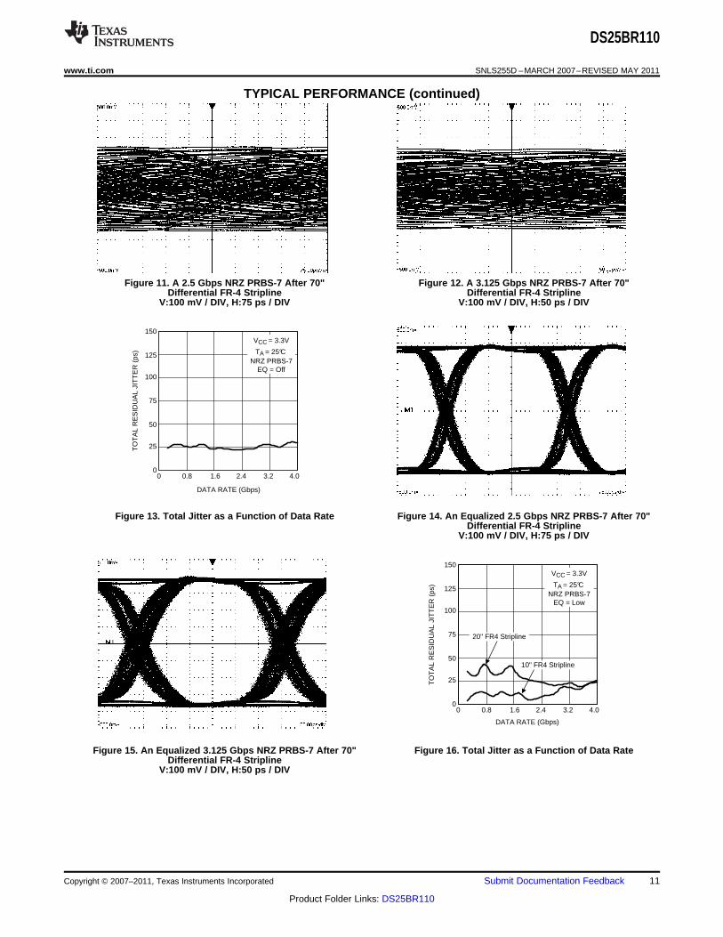
TYPICAL PERFORMANCE
Figure 5. Maximum Data Rate as a Function of CAT5e Figure 6. Maximum Data Rate as a Function of CAT7(Belden 1700A) Length (Siemon Tera) Length
Figure 7. Maximum Data Rate as a Function of CAT5e Figure 8. Maximum Data Rate as a Function of CAT5e(Belden 1700A) Length (Belden 1700A) Length
DS25BR120 Used as a DriverDS25BR110 Used as a Receiver
Figure 9. Maximum Data Rate as a Function of CAT7 Figure 10. Maximum Data Rate as a Function of CAT5e(Siemon Tera) Length (Belden 1700A) Length
DS25BR120 Used as a DriverDS25BR110 Used as a Receiver
10 Submit Documentation Feedback Copyright © 2007–2011, Texas Instruments Incorporated
Product Folder Links: DS25BR110
150
125
100
75
50
25
00 0.8 1.6 2.4 3.2 4.0
VCC = 3.3V
TA = 25°CNRZ PRBS-7
EQ = Low
TO
TA
L R
ES
IDU
AL
JIT
TE
R (
ps)
DATA RATE (Gbps)
20" FR4 Stripline
10" FR4 Stripline
150
125
100
75
50
25
00 0.8 1.6 2.4 3.2 4.0
VCC = 3.3V
TA = 25°CNRZ PRBS-7
EQ = Off
TO
TA
L R
ES
IDU
AL
JIT
TE
R (
ps)
DATA RATE (Gbps)
DS25BR110
www.ti.com SNLS255D –MARCH 2007–REVISED MAY 2011
TYPICAL PERFORMANCE (continued)
Figure 11. A 2.5 Gbps NRZ PRBS-7 After 70" Figure 12. A 3.125 Gbps NRZ PRBS-7 After 70"Differential FR-4 Stripline Differential FR-4 Stripline
V:100 mV / DIV, H:75 ps / DIV V:100 mV / DIV, H:50 ps / DIV
Figure 13. Total Jitter as a Function of Data Rate Figure 14. An Equalized 2.5 Gbps NRZ PRBS-7 After 70"Differential FR-4 Stripline
V:100 mV / DIV, H:75 ps / DIV
Figure 15. An Equalized 3.125 Gbps NRZ PRBS-7 After 70" Figure 16. Total Jitter as a Function of Data RateDifferential FR-4 Stripline
V:100 mV / DIV, H:50 ps / DIV
Copyright © 2007–2011, Texas Instruments Incorporated Submit Documentation Feedback 11
Product Folder Links: DS25BR110

150
125
100
75
50
25
00.25 0.40 0.55 0.70 0.85 1.00
VCC = 3.3V
TA = 25°CNRZ PRBS-7
2.5 Gbps
TO
TA
L R
ES
IDU
AL
JIT
TE
R (
ps)
DIFFERENTIAL INPUT VOLTAGE (V)
30" FR4, EQ = Medium
60" FR4, EQ = High
150
125
100
75
50
25
00.25 0.40 0.55 0.70 0.85 1.00
VCC = 3.3V
TA = 25°CNRZ PRBS-73.125 Gbps
TO
TA
L R
ES
IDU
AL
JIT
TE
R (
ps)
DIFFERENTIAL INPUT VOLTAGE (V)
30" FR4, EQ = Medium
60" FR4, EQ = High
150
125
100
75
50
25
00 0.8 1.6 2.4 3.2 4.0
VCC = 3.3V
TA = 25°CNRZ PRBS-7
EQ = High
TO
TA
L R
ES
IDU
AL
JIT
TE
R (
ps)
DATA RATE (Gbps)
40" FR4 Stripline
50" FR4 Stripline
70" FR4 Stripline
60" FR4 Stripline
150
125
100
75
50
25
00.25 0.40 0.55 0.70 0.85 1.00
VCC = 3.3V
TA = 25°CNRZ PRBS-73.125 Gbps
TO
TA
L R
ES
IDU
AL
JIT
TE
R (
ps)
DIFFERENTIAL INPUT VOLTAGE (V)
4" FR4, EQ = Off
15" FR4, EQ = Low
150
125
100
75
50
25
00 0.8 1.6 2.4 3.2 4.0
VCC = 3.3V
TA = 25°CNRZ PRBS-7EQ = Medium
TO
TA
L R
ES
IDU
AL
JIT
TE
R (
ps)
DATA RATE (Gbps)
30" FR4 Stripline
20" FR4 Stripline
40" FR4 Stripline
150
125
100
75
50
25
00.25 0.40 0.55 0.70 0.85 1.00
VCC = 3.3V
TA = 25°CNRZ PRBS-7
2.5 Gbps
TO
TA
L R
ES
IDU
AL
JIT
TE
R (
ps)
DIFFERENTIAL INPUT VOLTAGE (V)
4" FR4, EQ = Off
15" FR4, EQ = Low
DS25BR110
SNLS255D –MARCH 2007–REVISED MAY 2011 www.ti.com
TYPICAL PERFORMANCE (continued)
Figure 17. Total Jitter as a Function of Data Rate Figure 18. Total Jitter as a Function of Input Amplitude
Figure 19. Total Jitter as a Function of Input Amplitude Figure 20. Total Jitter as a Function of Data Rate
Figure 21. Total Jitter as a Function of Input Amplitude Figure 22. Total Jitter as a Function of Input Amplitude
12 Submit Documentation Feedback Copyright © 2007–2011, Texas Instruments Incorporated
Product Folder Links: DS25BR110
PACKAGE OPTION ADDENDUM
www.ti.com 17-Nov-2012
Addendum-Page 1
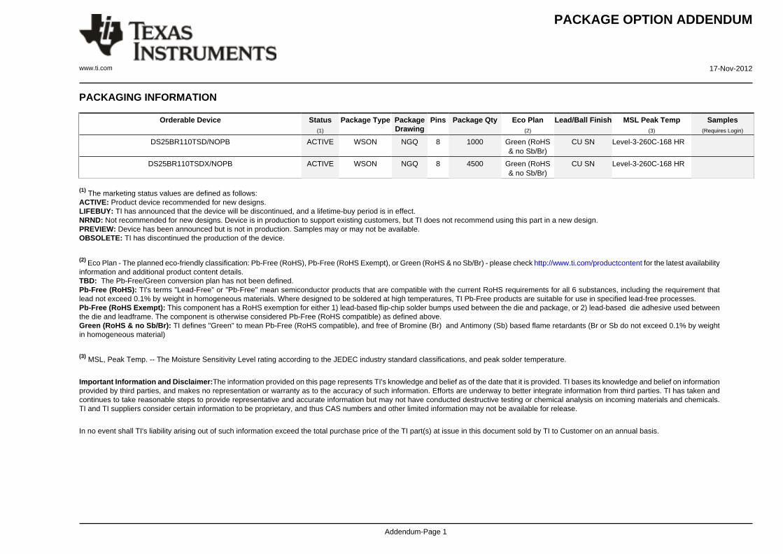
PACKAGING INFORMATION
Orderable Device Status(1)
Package Type PackageDrawing
Pins Package Qty Eco Plan(2)
Lead/Ball Finish MSL Peak Temp(3)
Samples(Requires Login)
DS25BR110TSD/NOPB ACTIVE WSON NGQ 8 1000 Green (RoHS& no Sb/Br)
CU SN Level-3-260C-168 HR
DS25BR110TSDX/NOPB ACTIVE WSON NGQ 8 4500 Green (RoHS& no Sb/Br)
CU SN Level-3-260C-168 HR
(1) The marketing status values are defined as follows:ACTIVE: Product device recommended for new designs.LIFEBUY: TI has announced that the device will be discontinued, and a lifetime-buy period is in effect.NRND: Not recommended for new designs. Device is in production to support existing customers, but TI does not recommend using this part in a new design.PREVIEW: Device has been announced but is not in production. Samples may or may not be available.OBSOLETE: TI has discontinued the production of the device.
(2) Eco Plan - The planned eco-friendly classification: Pb-Free (RoHS), Pb-Free (RoHS Exempt), or Green (RoHS & no Sb/Br) - please check http://www.ti.com/productcontent for the latest availabilityinformation and additional product content details.TBD: The Pb-Free/Green conversion plan has not been defined.Pb-Free (RoHS): TI's terms "Lead-Free" or "Pb-Free" mean semiconductor products that are compatible with the current RoHS requirements for all 6 substances, including the requirement thatlead not exceed 0.1% by weight in homogeneous materials. Where designed to be soldered at high temperatures, TI Pb-Free products are suitable for use in specified lead-free processes.Pb-Free (RoHS Exempt): This component has a RoHS exemption for either 1) lead-based flip-chip solder bumps used between the die and package, or 2) lead-based die adhesive used betweenthe die and leadframe. The component is otherwise considered Pb-Free (RoHS compatible) as defined above.Green (RoHS & no Sb/Br): TI defines "Green" to mean Pb-Free (RoHS compatible), and free of Bromine (Br) and Antimony (Sb) based flame retardants (Br or Sb do not exceed 0.1% by weightin homogeneous material)
(3) MSL, Peak Temp. -- The Moisture Sensitivity Level rating according to the JEDEC industry standard classifications, and peak solder temperature.
Important Information and Disclaimer:The information provided on this page represents TI's knowledge and belief as of the date that it is provided. TI bases its knowledge and belief on informationprovided by third parties, and makes no representation or warranty as to the accuracy of such information. Efforts are underway to better integrate information from third parties. TI has taken andcontinues to take reasonable steps to provide representative and accurate information but may not have conducted destructive testing or chemical analysis on incoming materials and chemicals.TI and TI suppliers consider certain information to be proprietary, and thus CAS numbers and other limited information may not be available for release.
In no event shall TI's liability arising out of such information exceed the total purchase price of the TI part(s) at issue in this document sold by TI to Customer on an annual basis.

TAPE AND REEL INFORMATION
*All dimensions are nominal
Device PackageType
PackageDrawing
Pins SPQ ReelDiameter
(mm)
ReelWidth
W1 (mm)
A0(mm)
B0(mm)
K0(mm)
P1(mm)
W(mm)
Pin1Quadrant
DS25BR110TSD/NOPB WSON NGQ 8 1000 178.0 12.4 3.3 3.3 1.0 8.0 12.0 Q1
DS25BR110TSDX/NOPB WSON NGQ 8 4500 330.0 12.4 3.3 3.3 1.0 8.0 12.0 Q1
PACKAGE MATERIALS INFORMATION
www.ti.com 17-Nov-2012
Pack Materials-Page 1
*All dimensions are nominal
Device Package Type Package Drawing Pins SPQ Length (mm) Width (mm) Height (mm)
DS25BR110TSD/NOPB WSON NGQ 8 1000 203.0 190.0 41.0
DS25BR110TSDX/NOPB WSON NGQ 8 4500 358.0 343.0 63.0
PACKAGE MATERIALS INFORMATION
www.ti.com 17-Nov-2012
Pack Materials-Page 2
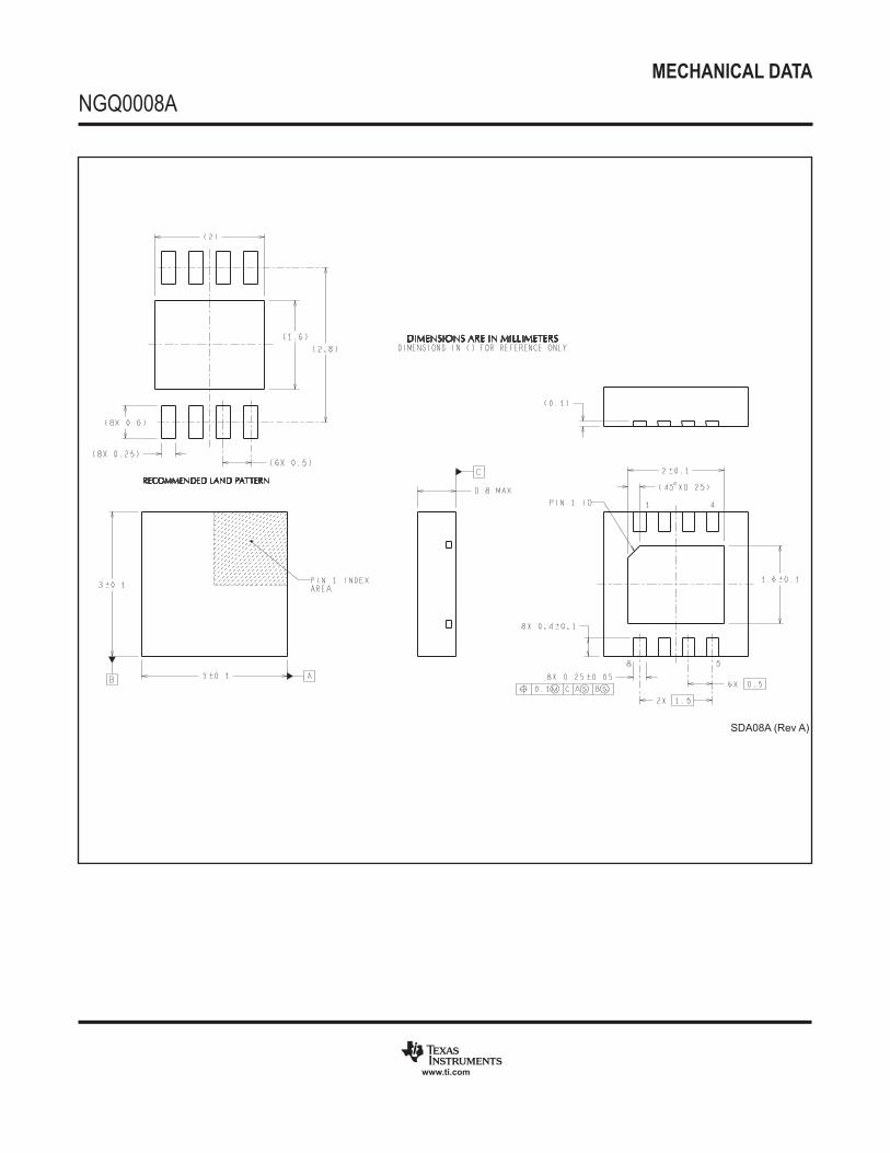
MECHANICAL DATA
NGQ0008A
www.ti.com
SDA08A (Rev A)

IMPORTANT NOTICE
Texas Instruments Incorporated and its subsidiaries (TI) reserve the right to make corrections, enhancements, improvements and otherchanges to its semiconductor products and services per JESD46, latest issue, and to discontinue any product or service per JESD48, latestissue. Buyers should obtain the latest relevant information before placing orders and should verify that such information is current andcomplete. All semiconductor products (also referred to herein as “components”) are sold subject to TI’s terms and conditions of salesupplied at the time of order acknowledgment.
TI warrants performance of its components to the specifications applicable at the time of sale, in accordance with the warranty in TI’s termsand conditions of sale of semiconductor products. Testing and other quality control techniques are used to the extent TI deems necessaryto support this warranty. Except where mandated by applicable law, testing of all parameters of each component is not necessarilyperformed.
TI assumes no liability for applications assistance or the design of Buyers’ products. Buyers are responsible for their products andapplications using TI components. To minimize the risks associated with Buyers’ products and applications, Buyers should provideadequate design and operating safeguards.
TI does not warrant or represent that any license, either express or implied, is granted under any patent right, copyright, mask work right, orother intellectual property right relating to any combination, machine, or process in which TI components or services are used. Informationpublished by TI regarding third-party products or services does not constitute a license to use such products or services or a warranty orendorsement thereof. Use of such information may require a license from a third party under the patents or other intellectual property of thethird party, or a license from TI under the patents or other intellectual property of TI.
Reproduction of significant portions of TI information in TI data books or data sheets is permissible only if reproduction is without alterationand is accompanied by all associated warranties, conditions, limitations, and notices. TI is not responsible or liable for such altereddocumentation. Information of third parties may be subject to additional restrictions.
Resale of TI components or services with statements different from or beyond the parameters stated by TI for that component or servicevoids all express and any implied warranties for the associated TI component or service and is an unfair and deceptive business practice.TI is not responsible or liable for any such statements.
Buyer acknowledges and agrees that it is solely responsible for compliance with all legal, regulatory and safety-related requirementsconcerning its products, and any use of TI components in its applications, notwithstanding any applications-related information or supportthat may be provided by TI. Buyer represents and agrees that it has all the necessary expertise to create and implement safeguards whichanticipate dangerous consequences of failures, monitor failures and their consequences, lessen the likelihood of failures that might causeharm and take appropriate remedial actions. Buyer will fully indemnify TI and its representatives against any damages arising out of the useof any TI components in safety-critical applications.
In some cases, TI components may be promoted specifically to facilitate safety-related applications. With such components, TI’s goal is tohelp enable customers to design and create their own end-product solutions that meet applicable functional safety standards andrequirements. Nonetheless, such components are subject to these terms.
No TI components are authorized for use in FDA Class III (or similar life-critical medical equipment) unless authorized officers of the partieshave executed a special agreement specifically governing such use.
Only those TI components which TI has specifically designated as military grade or “enhanced plastic” are designed and intended for use inmilitary/aerospace applications or environments. Buyer acknowledges and agrees that any military or aerospace use of TI componentswhich have not been so designated is solely at the Buyer's risk, and that Buyer is solely responsible for compliance with all legal andregulatory requirements in connection with such use.
TI has specifically designated certain components as meeting ISO/TS16949 requirements, mainly for automotive use. In any case of use ofnon-designated products, TI will not be responsible for any failure to meet ISO/TS16949.
Products Applications
Audio www.ti.com/audio Automotive and Transportation www.ti.com/automotive
Amplifiers amplifier.ti.com Communications and Telecom www.ti.com/communications
Data Converters dataconverter.ti.com Computers and Peripherals www.ti.com/computers
DLP® Products www.dlp.com Consumer Electronics www.ti.com/consumer-apps
DSP dsp.ti.com Energy and Lighting www.ti.com/energy
Clocks and Timers www.ti.com/clocks Industrial www.ti.com/industrial
Interface interface.ti.com Medical www.ti.com/medical
Logic logic.ti.com Security www.ti.com/security
Power Mgmt power.ti.com Space, Avionics and Defense www.ti.com/space-avionics-defense
Microcontrollers microcontroller.ti.com Video and Imaging www.ti.com/video
RFID www.ti-rfid.com
OMAP Applications Processors www.ti.com/omap TI E2E Community e2e.ti.com
Wireless Connectivity www.ti.com/wirelessconnectivity
Mailing Address: Texas Instruments, Post Office Box 655303, Dallas, Texas 75265Copyright © 2012, Texas Instruments Incorporated
Mouser Electronics
Authorized Distributor
Click to View Pricing, Inventory, Delivery & Lifecycle Information: Texas Instruments:
DS25BR110TSD/NOPB DS25BR110TSDX/NOPB