Embed Size (px)
Citation preview

Innovative PowerTM - 1 - www.active-semi.com
Copyright © 2016-2017 Active-Semi, Inc.
FEATURES AEC-Q100 Automotive Qualified -40°C~125°C Junction Temperature Range
Automotive Qualified Passes SAE J1752 M8A EMC testing Quick Charge™ 2.0 Certified by Qualcomm®
and UL. UL Certificate No. 4787083099-1 http://www.qualcomm.com/documents/quickc
harge-device-list 40V Input Voltage Surge 4.5V-36V Operational Input Voltage 5.1V/9.1V/12.1V Output with +/-1% Accuracy Up to 3.0A Output current Constant Current Regulation Limit QC2.0 + Auto-Detect + USB-PD Type-C Support Hiccup Mode Protection at Output Short >90% Efficiency at Full Load 0.5mA Low Standby Input Current 5.7V/10.1V/13.5V Output Over-voltage
Protection for 5.1V/9.1V/12.1V Outputs Cord Voltage Compensation Meet EN55022 Class B Radiated EMI Standard 8kV ESD HBM Protection on DP and DM SOP-8EP Package
APPLICATIONS Automotive Applications Car Charger Cigarette Lighter Adaptor (CLA) CV/CC regulation DC/DC converter
GENERAL DESCRIPTION ACT4529 is a wide input voltage, high efficiency step-down DC/DC converter that operates in either CV (Constant Output Voltage) mode or CC (Constant Output Current) mode. This device has QC2.0 built in to provide 5.1V/9.1V/12.1V outputs as requested by attached portable devices. Besides building in QC2.0 decoding, it also supports Apple, Samsung and BC1.2 devices to charge at full current rate. ACT4529 has an interface for USB-PD control via a tri-state digital pin. Vout is 5.1V if this pin is floating, Vout is 9.1V when this pin voltage is less than 0.8V and Vout is 12.1V while this pin voltage is more than 2.0V.
ACT4529 has accurate output current limits under constant current regulation. It provides up to 3.0A output current at 125kHz switching frequency. ACT4529 utilizes adaptive drive technique to achieve good EMI performance while main >90% efficiency at full load for mini size CLA designs. It also has output short circuit protection with hiccup mode. The average output current is reduced to below 6mA when output is shorted to ground. Other features include output over voltage protection and thermal shutdown.
This device is available in a SOP-8EP package and requires very few external components for operation.
For details on SAE J1752 M8A EMC performance and testing, refer to Active-Semi application note AN-106, ACT4529M Automotive EMC Performance.
ACT4529M
40V/3.0A CV/CC Buck Converter Featuring QC2.0, USB Auto-Detect and USB-PD
Rev 1, 23-Feb-17
Typical Application Circuit V/I Profile
* Patent Pending

ACT4529M Rev 1, 23-Feb-17
Innovative PowerTM - 2 - www.active-semi.com
Copyright © 2016-2017 Active-Semi, Inc.
ORDERING INFORMATION
PIN CONFIGURATION
Top View
PART NUMBER PDC USB AUTO DETECT QC2.0 CERTIFICATION PACKAGE
ACT4529MYH-T0010 Yes No Yes QC 2.0 SOP-8EP
ACT4529MYH-T1011 Yes Yes Yes N/A SOP-8EP

ACT4529M Rev 1, 23-Feb-17
Innovative PowerTM - 3 - www.active-semi.com
Copyright © 2016-2017 Active-Semi, Inc.
ABSOLUTE MAXIMUM RATINGS
PARAMETER VALUE UNIT
IN to GND -0.3 to 40 V
SW to GND -1 to VIN +1 V
HSB to GND VSW - 0.3 to VSW + 7 V
CSP, CSN to GND -0.3 to +15 V
Junction to Ambient Thermal Resistance 46 °C/W
Operating Junction Temperature -40 to 150 °C
Storage Junction Temperature -55 to 150 °C
Lead Temperature (Soldering 10 sec.) 300 °C
All other pins to GND -0.3 to +6 V
PDC to GND -0.3 to +6 V
: Do not exceed these limits to prevent damage to the device. Exposure to absolute maximum rating conditions for long periods may affect device reliability.
PIN DESCRIPTIONS
PIN NAME DESCRIPTION
1 CSP Voltage Feedback Input. Connect to node of the inductor and output capacitor. CSP and CSN Kevin sense is recommended.
2 CSN Negative input terminal of output current sense. Connect to the negative terminal of current sense resistor.
3 PDC USB-PD Control Pin. floating: 5.1V, pulled high: 12.1V, pulled low: 9.1V. Do not drive this pin higher than 5V.
4 DP Data Line Positive Input. Connected to D+ of attached portable device data line. This pin passes 8kV HBM ESD.
5 DM Data Line Negative Input. Connected to D- of attached portable device data line. This pin passes 8kV HBM ESD.
6 IN Power Supply Input. Bypass this pin with a 10μF ceramic capacitor to GND, placed as close to the IC as possible.
7 SW Power Switching Output to External Inductor.
8 HSB High Side Bias Pin. This provides power to the internal high-side MOSFET gate driver. Connect a 22nF capacitor from HSB pin to SW pin.
9 GND Ground and Heat Dissipation Pad. Connect this exposed pad to large ground copper area with copper and vias.

ACT4529M Rev 1, 23-Feb-17
Innovative PowerTM - 4 - www.active-semi.com
Copyright © 2016-2017 Active-Semi, Inc.
Parameter Symbol Condition Min Typ Max Units
Input Over Voltage Protection VIN_OVP Rising 40 42 44 V
Input Over Voltage Hysteresis 4 V
Input Over Voltage Response Time T_VIN_OVP VIN step from 30V to 45V 250 ns
Input Under Voltage Lockout (UVLO) VIN Rising 4.15 4.5 4.75 V
Input UVLO Hysteresis 200 mV
Input Voltage Power Good Deglitch Time No OVP 40 ms
Input Voltage Power Good Deglitch Time No UVP 10 us
Input Standby Current Vin=12V, Vout=5.1V, Iload=0 500 uA
Output Voltage Regulation CSP At Full Temperature
4.92
8.78
11.67
5.1
9.1
12.1
5.28
9.42
12.53
V
Output Voltage Regulation CSP At Room Temperature
5.05
9.0
11.95
5.1
9.1
12.1
5.15
9.2
12.25
V
Output Over Voltage Protection (OVP) Output rising
5.5
9.7
13.0
5.7
10.1
13.5
6.0
10.5
14.0
V
Input Brownout Protection
(ACT4529MYH-T1011 only)
VIN Drop Threshold
Falling Threshold 7.5 8.0 8.5 V
Hysteresis 200 mV
Vout Drop Delay Time 416 480 ms
QC and PDC Restart time 416 480 ms
Output Over Voltage Deglitch Time 1.0 us
Output Voltage Cord Compensation
ACT 4529MYH-
T0010 66mV between CSP and CSN
-25% 200 +25% mV
ACT 4529MYH-
T1011 -25% 200 +25% mV
Output Under Voltage Protection (UVP) VOUT VOUT falling -10% 3.2 10% V
UVP Hysteresis VOUT VOUT rising 0.55 V
UVP Deglitch Time VOUT 10 us
UVP Blanking Time at Startup 3.5 ms
ELECTRICAL CHARACTERISTICS (VIN = 12V, TJ = -40°C~125°C, , unless otherwise specified.)

ACT4529M Rev 1, 23-Feb-17
Innovative PowerTM - 5 - www.active-semi.com
Copyright © 2016-2017 Active-Semi, Inc.
Parameter Symbol Condition Min Typ Max Units
Output Constant Current Limit Rcs=20mΩ 2.95 3.3 3.63 A
Hiccup Waiting Time 4.13 S
Top FET Cycle by Cycle Current Limit 4.5 5.8 A
Top FET Rds on 70 mΩ
Bot FET Rds on 4.7 Ω
Maximum Duty Cycle 99 %
Switching Frequency -10% 125 +10% kHz
Soft-start Time 2.0 ms
Out Voltage Ripples Cout=220uF/22uF ceramic 80 mV
VOUT Discharge Current For high to lower voltage transi-tions 60 mA
Voltage transition time for QC 2.0 transition or USB PD Type C 12V-5V 100 ms
Voltage transition time for QC 2.0 transition or USB PD Type C 5V-12V 100 ms
Line Transient Response Input 12V-40V-12V with 1V/us slew rate, Vout=5V, Iload=0A and 2.4A
4.75 5.25 V
Load Transient Response
Vout=5V 80mA-1.0A-80mA load with 0.1A/us slew rate 4.9 5.15 5.4 V
Vout=9V 80mA-1.0A-80mA load with 0.1A/us slew rate 8.7 9.1 9.5 V
Vout=12V 80mA-1.0A-80mA load with 0.1A/us slew rate 11.6 12.1 12.6 V
Thermal Shut Down 160 °C
Thermal Shut Down Hysteresis 30 °C
ESD of DP, DM HBM 8 kV
PDC High Threshold 2.2 V
PDC Low Threshold 0.6 V
PDC Drive Current 10 uA
ELECTRICAL CHARACTERISTICS (VIN = 12V, TJ = -40°C~125°C, unless otherwise specified.)

ACT4529M Rev 1, 23-Feb-17
Innovative PowerTM - 6 - www.active-semi.com
Copyright © 2016-2017 Active-Semi, Inc.
FUNCTIONAL BLOCK DIAGRAM
FUNCTIONAL DESCRIPTION
Output Current Sensing and Regulation
Sense resistor is connected to CSP and CSN. The sensed differential voltage is compared with interval reference to regulate current. CC loop and CV loop are in parallel. The current loop response is allowed to have slower response compared to voltage loop. However, during current transient response, the inductor current overshoot/undershoot should be controlled within +/-25% to avoid inductor saturation.
Cycle-by-Cycle Current Control
The conventional cycle-by-cycle peak current mode is implemented with high-side FET current sense.
Input Over Voltage Protection
The converter is disabled if the input voltage is above 42V (+/-2V). Device resumes operation automatically 40ms after OVP is cleared.
Output Over Voltage Protection
Device stops switching when output over-voltage is sensed, and resumes operation automatically when output voltage drops to OVP- hysteresis.
Output Over Voltage Discharge
Discharge circuit starts to discharge output through CSP pins when output over voltage is detected. Discharge circuit brings 12V down to 5V in less than 100ms.
Output Under-Voltage Protection / Hiccup Mode
There is a under voltage protection (UVP) threshold. If the UVP threshold is hit for 10us, an over current or short circuit is assumed, and the converter goes into hiccup mode by disabling the converter and restarts after hiccup waiting period.
Input Brownout Protection (ACT4529MYH-T1011 only)
If the input voltage drops below 8V but higher than UVLO for 450ms while in QC or PDC mode, the output voltage turns off and QC or PDC mode is disabled. If the output voltage drops below 3.7V, the timer restarts and waits for 450ms before attempting to restart the output voltage. When output voltage rises above 3.9V and detects the input voltage below 8V, timer restarts. If the input voltage is below 8V after 450ms, the output turns off. The cycle continues until the input voltage increases above 8.2V,for longer than 450ms, then output turns on, the IC renegotiates the PD and QC protocols, and normal operation restarts.
Thermal Shutdown
If the TJ increases beyond 160°C, ACT4529 goes into HZ mode and the timer is preserved until TJ drops by 30°C.

ACT4529M Rev 1, 23-Feb-17
Innovative PowerTM - 7 - www.active-semi.com
Copyright © 2016-2017 Active-Semi, Inc.
Cord Compensation
Cord Compensation increases the output voltage with increased output current to compensate for the voltage drop across the output connector and output cable.
The compensation voltage is derived as:
ΔVout = RCS*Iout*K
Where RCS is the current sense resistance, Iout is the load current, and K = 3.03
FUNCTIONAL DESCRIPTION

ACT4529M Rev 1, 23-Feb-17
Innovative PowerTM - 8 - www.active-semi.com
Copyright © 2016-2017 Active-Semi, Inc.
APPLICATIONS INFORMATION
Inductor Selection The inductor maintains a continuous current to the output load. This inductor current has a ripple that is dependent on the inductance value.
Higher inductance reduces the peak-to-peak ripple current. The trade off for high inductance value is the increase in inductor core size and series resistance, and the reduction in current handling capability. In general, select an inductance value L based on ripple current requirement:
Where VIN is the input voltage, VOUT is the output voltage, fSW is the switching frequency, ILOADMAX is the maximum load current, and KRIPPLE is the ripple factor. Typically, choose KRIPPLE = 30% to correspond to the peak-to-peak ripple current being 30% of the maximum load current.
With a selected inductor value the peak-to-peak inductor current is estimated as:
The peak inductor current is estimated as:
The selected inductor should not saturate at ILPK. The maximum output current is calculated as:
LLIM is the internal current limit.
Input Capacitor The input capacitor needs to be carefully selected to maintain sufficiently low ripple at the supply input of the converter. A low ESR capacitor is highly recommended. Since large current flows in and out of this capacitor during switching, its ESR also affects efficiency.
The input capacitance needs to be higher than 10µF. The best choice is the ceramic type. However, low ESR tantalum or electrolytic types
may also be used provided that the RMS ripple current rating is higher than 50% of the output current. The input capacitor should be placed close to the IN and GND pins of the IC, with the shortest traces possible. In the case of tantalum or electrolytic types, a ceramic capacitor is recommended to parallel with tantalum or electrolytic capacitor, which should be placed right next to the IC.
Output Capacitor The output capacitor also needs to have low ESR to keep low output voltage ripple. The output ripple voltage is:
Where IOUTMAX is the maximum output current, KRIPPLE is the ripple factor, RESR is the ESR of the output capacitor, fSW is the switching frequency, L is the inductor value, and COUT is the output capacitance. From the equation above, VRIPPLE is the combination of ESR and real capacitance. In the case of ceramic output capacitors, RESR is very small and does not contribute to the ripple. Therefore, a lower capacitance value can be used for ceramic type. In the case of tantalum or electrolytic capacitors, the ripple is dominated by RESR multiplied by the ripple current. In that case, the output capacitor is chosen to have sufficiently low ESR.
For ceramic output capacitor, typically choose a capacitance of about 22µF. For tantalum or electrolytic capacitors, choose a capacitor with less than 50mΩ ESR. When 330uF or 470uF electrolytic cap or tantalum cap is used, where ripple is dominantly caused by ESR, a 2.2uF ceramic in parallel is recommended.
Rectifier Schottky Diode Use a Schottky diode as the rectifier to conduct current when the High-Side Power Switch is off. The Schottky diode must have current rating higher than the maximum output current and a reverse voltage rating higher than the maximum input voltage. Further more, the low forward voltage Schottky is preferable for high efficiency and smoothly operation.
(1)
(2)
(3)
(4)
(5)

ACT4529M Rev 1, 23-Feb-17
Innovative PowerTM - 9 - www.active-semi.com
Copyright © 2016-2017 Active-Semi, Inc.
Current Sense Resistors
The traces leading to and from the sense resistor can be significant error sources. With small value sense resistors, trace resistance shared with the load can cause significant errors. It is recommended to connect the sense resistor pads directly to the CSP and CSN pins using “Kelvin” or “4-wire” connection techniques as shown below.
Current Limit Setting When the output current reaches current limit, the IC limits the peak switch current on a cycle-by-cycle basis. This reduces the output voltage to keep the output current at a constant value.
The following equation calculates the peak current limit.
Where Rcs is current sense resistor.
The maximum output current is defined by
APPLICATIONS INFORMATION
(6)
(7)

ACT4529M Rev 1, 23-Feb-17
Innovative PowerTM - 10 - www.active-semi.com
Copyright © 2016-2017 Active-Semi, Inc.
APPLICATIONS INFORMATION
PCB Layout Guidance When laying out the printed circuit board, the following checklist should be used to ensure proper operation of the IC.
1) Arrange the power components to reduce the AC loop size consisting of CIN, IN pin, SW pin, the Schottky diode, and GND
2) Place input decoupling ceramic capacitor CIN as close to VIN pin as possible. The GND side of CIN must be placed as close as possible to to power GND on the top layer. The traces should be short and wide.
3) The high power loss components, e.g. the controller, Schottky diode, and the inductor should be placed carefully to make the thermal spread evenly on the board.
4) Schottky anode pad and IC exposed pad should be placed close to ground clips in CLA applications
5) Use “Kelvin” or “4-wire” connection techniques from the sense resistor pads directly to the CSP and CSN pins. The CSP and CSN traces should be in parallel to avoid interference.
6) Place multiple vias between top and bottom GND planes for best heat dissipation and noise immunity.
7) Use short traces connecting HSB-CHSB-SW loop.
8) SW node is noisy, switching from VIN to GND. Its size should be minimized and it should be isolated away from the rest of circuit for good EMI and low noise operation.
Example PCB Layout
ACT4529M Rev 1, 23-Feb-17
Innovative PowerTM - 11 - www.active-semi.com
Copyright © 2016-2017 Active-Semi, Inc.
BOM List for 2.4A Car Charger
ITEM REFERENCE DESCRIPTION MANUFACTURER QTY
1 U1 IC, ACT4529, SOP-8EP Active-Semi 1
2 C1 Capacitor, Electrolytic, 47µF/35V Murata, TDK 1
3 C2 Capacitor, Ceramic, 10µF/25V, 1206, SMD Murata, TDK 1
4 C3 Capacitor, Ceramic, 22nF/25V, 0603, SMD Murata, TDK 1
5 C4 Capacitor, Ceramic, 22µF/16V, 1206, SMD Murata, TDK 1
6 C5 Capacitor, Electrolytic, 220µF/16V Murata, TDK 1
7 C6 Capacitor, Ceramic, 2.2µF/16V, 0805, SMD Murata, TDK 1
8 L1 Inductor, 40µH, 4A, 20% 1
9 D1 Diode, Schottky, 40V/5A, SK54L Panjit 1
10 Rcs Chip Resistor, 20mΩ, 1206, 1% Murata, TDK 1
Typical Application Circuit

ACT4529M Rev 1, 23-Feb-17
Innovative PowerTM - 12 - www.active-semi.com
Copyright © 2016-2017 Active-Semi, Inc.
TYPICAL PERFORMANCE CHARACTERISTICS
(Schematic as show in typical application circuit, Ta = 25°C, unless otherwise specified)
Eff
icie
ncy
(%)
100
85
80
75
70
65
60
95
90
Efficiency vs. Load current ( 5V Vout)
AC
T45
29-00
1
VIN =12V
VIN =24V
Eff
icie
ncy(
%) VIN =24V
AC
T45
29-00
2
VIN =12V
0 500 1000 1500 2000 2500 3000
Load Current (mA)
100
85
80
75
70
65
60
95
90
Efficiency vs. Load current ( 9V Vout)
0 500 1000 1500 2000 2500 3000
Load Current (mA)
Eff
icie
ncy
(%)
100
85
80
75
70
65
60
95
90
Efficiency vs. Load current ( 12V Vout)
AC
T45
29-00
3 VIN =24V VIN =12V
Output CC/CV Curve (5V Vout)
Out
put V
olta
ge (
V)
6.0
5.0
4.0
3.0
2.0
1.0
0
VIN =24V VIN =12V
AC
T45
29-00
4
Output CC/CV Curve (9V Vout)
Out
put V
olta
ge (
V)
10.0
8.0
6.0
4.0
2.0
0
AC
T45
29-00
5
Output CC/CV Curve (12V Vout)
Out
put V
olta
ge (
V)
12.0
10.0
8.0
6.0
4.0
2.0
0
14.0
VIN =24V VIN =12V
AC
T45
29-00
6
VIN =24V
VIN =12V
0 500 1000 1500 2000 2500 3000
Load Current (mA)
0 5000 1000 1500 2000 2500 3000 3500
Output Current (mA)
0 5000 1000 1500 2000 2500 3000 3500
Output Current (mA)
0 5000 1000 1500 2000 2500 3000 3500
Output Current (mA)

ACT4529M Rev 1, 23-Feb-17
Innovative PowerTM - 13 - www.active-semi.com
Copyright © 2016-2017 Active-Semi, Inc.
TYPICAL PERFORMANCE CHARACTERISTICS
(Schematic as show in typical application circuit, Ta = 25°C, unless otherwise specified)
Load Transient (80mA-1A-80mA) Vin=12V, Vout=5V
AC
T45
29-00
9
CH1: VOUT, 100mV/div CH2: IOUT, 1A/div TIME: 400us//div
CH1
CH2
Load Transient (1A-2.4A-1A) Vin=12V, Vout=5V
AC
T45
29-01
0
CH1: VOUT, 200mV/div CH2: IOUT, 1A/div TIME: 400us//div
CH1
CH2
Load Transient (80mA-1A-80mA) Vin=12.6V, Vout=12V
AC
T45
29-01
1
CH1: VOUT, 200mV/div CH2: IOUT, 1A/div TIME: 400us//div
CH1
CH2
Load Transient (1A-2.4A-1A) Vin=12.6V, Vout=12V
AC
T45
29-01
2
CH1: VOUT, 200mV/div CH2: IOUT, 1A/div TIME: 400us//div
CH1
CH2
Start up into CC Mode
AC
T45
29-00
8 VOUT = 5.1V RLORD = 1.5Ω IOUT = 2.65A VIN = 12V
CH1: VIN, 10V/div CH2: VOUT, 2V/div CH3: IOUT, 2A/div TIME: 400µs/div
CH1
CH2
CH3
Output Over Voltage (5V Vout)
AC
T45
29-00
7 CH1: VOUT, 1V/div CH2: SW, 10V/div TIME: 1ms/div
CH1
CH2

ACT4529M Rev 1, 23-Feb-17
Innovative PowerTM - 14 - www.active-semi.com
Copyright © 2016-2017 Active-Semi, Inc.
TYPICAL PERFORMANCE CHARACTERISTICS
(Schematic as show in typical application circuit, Ta = 25°C, unless otherwise specified)
Voltage Transient (5V-9V)
AC
T45
29-01
3
CH1: VOUT, 2V/div TIME: 10ms//div
CH1
Voltage Transient (9V-5V)
AC
T45
29-01
4
CH1: VOUT, 2V/div TIME: 10ms//div
CH1
Voltage Transient (5V-12V)
AC
T45
29-01
5
CH1: VOUT, 2V/div TIME: 10ms//div
CH1
Voltage Transient (12V-5V)
AC
T45
29-01
6
CH1: VOUT, 2V/div TIME: 10ms//div
CH1
ACT4529M Rev 1, 23-Feb-17
Innovative PowerTM - 15 - www.active-semi.com
Copyright © 2016-2017 Active-Semi, Inc.
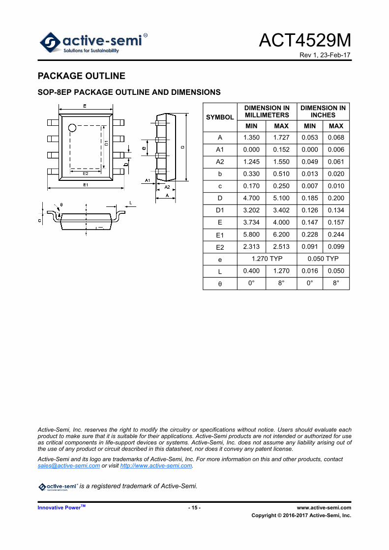
PACKAGE OUTLINE
SOP-8EP PACKAGE OUTLINE AND DIMENSIONS
Active-Semi, Inc. reserves the right to modify the circuitry or specifications without notice. Users should evaluate each product to make sure that it is suitable for their applications. Active-Semi products are not intended or authorized for use as critical components in life-support devices or systems. Active-Semi, Inc. does not assume any liability arising out of the use of any product or circuit described in this datasheet, nor does it convey any patent license.
Active-Semi and its logo are trademarks of Active-Semi, Inc. For more information on this and other products, contact [email protected] or visit http://www.active-semi.com.
is a registered trademark of Active-Semi.
SYMBOL
DIMENSION IN MILLIMETERS
DIMENSION IN INCHES
MIN MAX MIN MAX
A 1.350 1.727 0.053 0.068
A1 0.000 0.152 0.000 0.006
A2 1.245 1.550 0.049 0.061
b 0.330 0.510 0.013 0.020
c 0.170 0.250 0.007 0.010
D 4.700 5.100 0.185 0.200
D1 3.202 3.402 0.126 0.134
E 3.734 4.000 0.147 0.157
E1 5.800 6.200 0.228 0.244
E2 2.313 2.513 0.091 0.099
e 1.270 TYP 0.050 TYP
L 0.400 1.270 0.016 0.050
θ 0° 8° 0° 8°