Embed Size (px)
Citation preview

User's GuideSLVUA58–April 2014
DRV8307 User’s Guide
This document is provided with the DRV8307 customer evaluation module (EVM) as a supplement to theDRV8307 datasheet (SLVSCK2). It details the hardware implementation of the EVM.
Contents1 Printed-Circuit Board (PCB) (Top 3D View) .............................................................................. 22 Introduction ................................................................................................................... 2
2.1 Power Connectors .................................................................................................. 22.2 Test Points........................................................................................................... 32.3 Jumpers .............................................................................................................. 42.4 SPEED ADJUSTMENT (JP6) Jumper and (R20) Potentiometer............................................. 72.5 Operation of the EVM .............................................................................................. 8
3 Schematic and Bill of Materials ............................................................................................ 9
List of Figures
1 DRV8307EVM Top View.................................................................................................... 22 DRV8307EVM Test Points and FAULTn LED ........................................................................... 33 DRV8308EVM Jumpers..................................................................................................... 44 Hall PWR/GND Circuits ..................................................................................................... 55 Circuit when Setting Hall Power to “Current”............................................................................. 56 Switching Logic to Support Single-Ended and Differential-Hall Signals .............................................. 67 SPEED Adjustment Configuration ......................................................................................... 78 DRV8307EVM Schematic .................................................................................................. 9
List of Tables
1 Jumper Descriptions......................................................................................................... 42 Hall Sensors .................................................................................................................. 63 DRV8307EVM Bill of Materials ........................................................................................... 10
1SLVUA58–April 2014 DRV8307 User’s GuideSubmit Documentation Feedback
Copyright © 2014, Texas Instruments Incorporated

Printed-Circuit Board (PCB) (Top 3D View) www.ti.com
1 Printed-Circuit Board (PCB) (Top 3D View)Figure 1 illustrates the top view of the DRV8307 EVM PCB.
Figure 1. DRV8307EVM Top View
2 IntroductionThe DRV8307EVM is a solution for evaluating the DRV8307, a brushless DC motor controller. It includesa TLC555 timer configuration to supply PWM to the DRV8307, a potentiometer to adjust the speed of themotor by varying the duty cycle of the PWM, and an external PWM input pin. The EVM also supportsdifferential and single-ended hall sensors. The EVM includes surface-mounted test pins for all importantsignals on the board. The DRV8307EVM is configured so that only connections to the motor, hall sensorsand power supply are required.
2.1 Power ConnectorsThe DRV8307EVM uses a single power supply rail which must be connected to terminal P1. Minimumrecommended VM of the EVM is 8.5 V and maximum is 32 V, with a current of at least 2A. A highercurrent setting is recommended to maintain a stable VM voltage. Please refer to the DRV8307 datasheet(SLVSCK2) for complete voltage range information. When power is supplied to the board, a green LED(D4) in the lower left corner should light up.
2 DRV8307 User’s Guide SLVUA58–April 2014Submit Documentation Feedback
Copyright © 2014, Texas Instruments Incorporated

www.ti.com Introduction
2.2 Test PointsTest points are provided and labeled according to the inputs and outputs of the DRV8307 device. Thesignals brought out to test points are labeled HALLOUT, FAULTn, LOCKn, ENABLE, HU+/-, HV+/- HW+/-and GND (Figure 2).
Figure 2. DRV8307EVM Test Points and FAULTn LED
The HALLOUT signal represents the motor speed and phase information.RPM = (HALLOUT × 60) / pole pairs (1)
The FAULTn and LOCKn signals represent DRV8307 outputs and indicate a fault or lock condition of thedriver or motor. If there is a fault condition present, a red LED (D3) lights up. LOCKn indicates whether thespeed loop is locked.
The HU+/-, HV+/- HW+/- represent the corresponding hall signals. The ENABLE pin represents whetherthe DRV8307 is active or off.
The ENABLE signal is active low. The DRV8307 can be disabled by applying a high voltage to this pin.
3SLVUA58–April 2014 DRV8307 User’s GuideSubmit Documentation Feedback
Copyright © 2014, Texas Instruments Incorporated

Introduction www.ti.com
2.3 JumpersSeven jumpers (JP1–JP7) are installed by default on the EVM.
Table 1. Jumper Descriptions
Jumper DescriptionJP1 HALL POWER: Hall sensor power is “5V” or “current”JP2JP3 HALL SIGNALS: Hall Signals are “Differential” or “Single Ended”JP4JP5 DIRECTION: Motor direction is “forward” or “reverse”JP7 BRAKE: Motor brake “ON” or “OFF”JP6 SPEED: Speed input is from supplied “external” or “potentiometer”
The default jumper settings are JP1 2-3, JP2, JP3 1-2, JP4 2-3 and JP5, JP6, JP7 all installed. Thissupports "inverse" single-ended hall sensors supplied with 5 V. Speed is supplied from the potentiometerand the motor spins in a forward direction and is not braked.
Figure 3. DRV8308EVM Jumpers
4 DRV8307 User’s Guide SLVUA58–April 2014Submit Documentation Feedback
Copyright © 2014, Texas Instruments Incorporated

VM
2 k180 HPWRHGND
Hall Elements
DRV8307VSW
www.ti.com Introduction
2.3.1 HALL POWER Configuration (JP1/JP2 ) JumpersSensored BLDC motors typically use either Hall ICs or Hall elements. Most ICs can use 5-V power, whileelements typically have power pins that have an equivalent circuit of a resistor, and current must belimited to about 10 mA. In order to support both Hall sensor types the hall power needs to be configuredon the DRV8307EVM.
When installing JP1 2-3 and JP2, a 5-V power is supplied to terminal P3 to power the ICs. The used(VREG) voltage is only present when DRV8307 is enabled and regulated from VM (Figure 4).
Figure 4. Hall PWR/GND Circuits
By installing JP1 1-2 and uninstalling JP2, the circuit illustrated in Figure 5 is available for the Hallelements. The used (VSW) voltage is only present when DRV8307 is enabled. VSW equals VM.
Figure 5. Circuit when Setting Hall Power to “Current”
The current can be calculated as follows: If VM is 24 V, and 3 Hall elements having a resistance of 400 Ωare connected in parallel, 10.4 mA is supplied. Always refer to your Hall element specifications tounderstand the proper current. The purpose of the 180-Ω resistor is to bias-up the common mode voltageof Hall element differential signals, since the DRV8307 requires VICM between 1.5 V to 3.5 V.
If you are unsure of your motor’s Hall type, measure the resistance between the Hall power and groundwires. If it is < 250 Ω, they are likely Hall elements. Hall sensors are easily damaged if incorrect power isapplied.
2.3.2 HALL SIGNAL Configuration (JP3/JP4) JumpersHall sensors output either a differential signal pair, or a single-ended signal. You can tell which type yourmotor uses simply by counting the number of wires; a sensored BLDC typically has 3 phase wires, 2 Hallpower wires, and 3 or 6 Hall signal wires, so 8 total means single-ended, and 11 total means differential.
The DRV8307 has differential comparators on the Hall inputs, and they can also accommodate single-ended signals with the use of a few passive components. When using differential Halls, directly connectthe 6 Hall signals to the DRV8307 pins.
When using single-ended Halls, they require pull-ups. The DRV8307 comparator “-” pins should be biasedwith a middle voltage, so that a single-ended swing on the “+” pin is detected like a differential voltage.Connect single-ended hall wires to the "+" pins at P3 for normal Hall sensor types or to "-" pins for inverseHall sensors.
5SLVUA58–April 2014 DRV8307 User’s GuideSubmit Documentation Feedback
Copyright © 2014, Texas Instruments Incorporated
HALL_U+
HALL_U-
Block H+
IN
Block H-
IN
Switch BSwitch A
Switch A
Switch CSwitch B
Switch D
JP3
Switch C
Switch D
JP4
5 V
5 V
5 V
5 V
2 V
2 V
Terminal P3 DRV8307
1
2
3
1
2
3
Switch A Switch B
Introduction www.ti.com
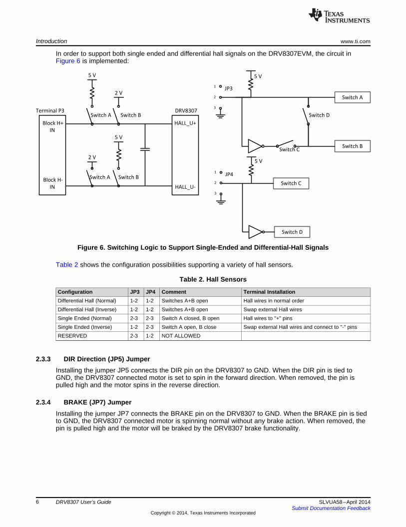
In order to support both single ended and differential hall signals on the DRV8307EVM, the circuit inFigure 6 is implemented:
Figure 6. Switching Logic to Support Single-Ended and Differential-Hall Signals
Table 2 shows the configuration possibilities supporting a variety of hall sensors.
Table 2. Hall Sensors
Configuration JP3 JP4 Comment Terminal InstallationDifferential Hall (Normal) 1-2 1-2 Switches A+B open Hall wires in normal orderDifferential Hall (Inverse) 1-2 1-2 Switches A+B open Swap external Hall wiresSingle Ended (Normal) 2-3 2-3 Switch A closed, B open Hall wires to "+" pinsSingle Ended (Inverse) 1-2 2-3 Switch A open, B close Swap external Hall wires and connect to "-" pinsRESERVED 2-3 1-2 NOT ALLOWED
2.3.3 DIR Direction (JP5) JumperInstalling the jumper JP5 connects the DIR pin on the DRV8307 to GND. When the DIR pin is tied toGND, the DRV8307 connected motor is set to spin in the forward direction. When removed, the pin ispulled high and the motor spins in the reverse direction.
2.3.4 BRAKE (JP7) JumperInstalling the jumper JP7 connects the BRAKE pin on the DRV8307 to GND. When the BRAKE pin is tiedto GND, the DRV8307 connected motor is spinning normal without any brake action. When removed, thepin is pulled high and the motor will be braked by the DRV8307 brake functionality.
6 DRV8307 User’s Guide SLVUA58–April 2014Submit Documentation Feedback
Copyright © 2014, Texas Instruments Incorporated

www.ti.com Introduction
2.4 SPEED ADJUSTMENT (JP6) Jumper and (R20) PotentiometerThe DRV8307 has a dedicated speed input pin (PWM) that supplies a duty cycle to the DRV8307 tocontrol motor speed.
Figure 7. SPEED Adjustment Configuration
The DRV8307EVM offers two possibilities to supply this PWM input, controlled by jumper JP6.
Installing JP6 uses the speed adjust potentiometer SPEED ADJUST (R20) as shown in Figure 7 as PWMspeed input. The potentiometer adjusts the duty cycle of the PWM signal which, in turn, adjusts the speedof the motor. The lower the duty cycle, therefore, the lower the speed, by turning the potentiometercounter-clockwise. In order to increase the duty cycle, thus increase the speed, turn the potentiometerclockwise.
The onboard PWM signal for the DRV8307 is generated by a circuit based upon TI's TLC555 Low-PowerTimer. It is capable of approximately a 25-kHz output that can be adjusted from 5% to 95% duty cycle.This square output signal will switch from 0 V to VREG.
In order to provide an external PWM signal to the DRV8307, remove JP6 and connect the external PWMsignal to JP6 pin 1 and the GND pin next to it. For more information on the PWM input required by theDRV8307, please refer to the DRV8307 datasheet (SLVSCK2).
7SLVUA58–April 2014 DRV8307 User’s GuideSubmit Documentation Feedback
Copyright © 2014, Texas Instruments Incorporated

Introduction www.ti.com
2.5 Operation of the EVMThe following steps provide instructions for the operation of the EVM:1. Connect a three-phase BLDC motor to terminal P2.2. Connect the hall signals, either single ended or differential, to terminal P3.3. Configure JP1-JP4 in order to supply the hall signals in the right manner to the DRV8307.4. Adjust the Speed potentiometer, R20, to minimum voltage by turning it all the way counterclockwise.
This minimizes the motor speed. Otherwise, connect your external PWM input to the JP6 PWM pin.5. Check JP5 and JP7 to be installed.6. Apply power to VM terminal P1.7. Adjust the potentiometer clockwise or turn your external PWM source ON to increase the speed of the
motor, continue adjusting as desired.8. To change direction, uninstall JP5.9. To start braking, uninstall JP7.
8 DRV8307 User’s Guide SLVUA58–April 2014Submit Documentation Feedback
Copyright © 2014, Texas Instruments Incorporated

ISENSEUHS_GATEUULS_GATEVLS_GATE
V VHS_GATE
WHS_GATEWWLS_GATE
DIR
BRAKE
PWM
ENABLE#
FAULTn
VINTHW-HW+HV-HV+HU-
VREG
CP1CP2VCP
HU+
VSW
GND
LOCKn
3KR14
1TP8
HALLOUT
1TP11
HU-
HU+1TP2
1TP3
HV-
HV+
HW-1TP5
1TP6
HW+
FAULTn
HALL OUT
GND
1TP13
30KR11 15K
R12
30KR13
1TP10
LOCKn
VM
VMGND
Connector forHall sensors
HW+
HW-
HV-
HV+
HU-
HU+
Test Points
Jumper List
JP3
JP4
JP1
Single Ended HALL
To provide 5V Hall power, install jumpers JP1_2-3 and JP2.
To provide current for Hall elements, install jumper JP1_1-2and uninstall JP2.
JP2
1TP7
ENABLE#
GND
1 2JP2
HPWR
VREGVSW
1 2 3
JP1
JP5
JP8
Red
12
D3
1TP1
In general, if the resistance between the Hall PWR andGND wires is <250 ohms, use "current". The purpose of
normal / inverse
1TP4
HGNDWH-WH+VH-VH+UH-UH+
1TP9
VM
HU+1
HU-2
HV+3
HV-4
HW+5
HW-6
VSW7
RSVD8
RSVD9
RSVD10
RS
VD
11
RS
VD
12
RS
VD
13
RS
VD
14
RS
VD
15
HA
LLO
UT
16
FA
ULT
n17
LO
CK
n18
PW
M19
BR
AK
E20
DIR21
ENABLE#22
RSVD23
VREG24
VINT25
GND26
VM27
VCP28
CP229
CP130
ISE
N31
UH
SG
32
U33
ULS
G34
VH
SG
35
V36
VLS
G37
WH
SG
38
W39
WLS
G40
PA
D41
U1
DRV8307
GND
the 180 ohm resistor is to bias-up the common-modevoltage of Hall elements that output differential signals.
54
123
678
P3
OSTTE080161
Default to populate:
JP1_2-3, JP2JP3_1-2, JP4_2-3
Hall power: 5V orcurrent
GND
30KR18VREG
VREG
VREG
VREG
30KR22
VREG
GND
12 JP5
30KR23
VREG
GND
12 JP7
180R17
2.0k
R16
0.1µFC10
0.1µFC11
0.1µFC12
0.1µFC13
0.1µFC15
0.1µFC171µFC16
1µFC14
VREG
VREG
PWM_X
THRES
GND1
TRIG2
OUT3
RESET4
CONT5
THRES6
DISCH7
VDD8
U5
TLC555
GND GND
THRES
GND
GND
555 Timer as PWM GeneratorApproximately 25 kHz
10kR21
0.01µFC3 0.1µF
C4
0.01µF
C5
D8
CW3
W2
CCW1
R20
D7
SN74CBT3244CPW
1OE#1
1A12
2B43
1A24
2B35
1A36
2B27
1A48
2B19
GND10
VCC20
2OE#19
1B118
2A417
1B216
2A315
1B314
2A213
1B412
2A111
U7
GND
VREG
0.1uF
C9
GND
SN74CBT3244CPW
1OE#1
1A12
2B43
1A24
2B35
1A36
2B27
1A48
2B19
GND10
VCC20
2OE#19
1B118
2A417
1B216
2A315
1B314
2A213
1B412
2A111
U8
SN74CBT3244CPW
1OE#1
1A12
2B43
1A24
2B35
1A36
2B27
1A48
2B19
GND10
VCC20
2OE#19
1B118
2A417
1B216
2A315
1B314
2A213
1B412
2A111
U91
2
3
JP4
GND
30KR2
VREG
16
52
U11ASN74LVC2G14DBVR
3 4
52
U11B
GND
VREG
GND
GND
VREG
0.1uF
C8
GND
VREG
0.1uF
C6
GND
3KR3
VREG
4.7uFC7
GND
15KR9
VREG
2V
3KR4
VREG
3KR5
VREG
HU-HV-HW-
HU+HV+HW+
HU-HV-HW-
HU+HV+HW+
1
2
3
JP3
GND
30KR1
VREG
GND
VREG
10.0kR10
4.7uFC20
GND
2V
GND
ISENSE
GND
A1
K2
D61.5SMC33
VHS_GATE
VLS_GATE
WHS_GATE
WLS_GATE
UHS_GATE
ULS_GATE
VM
S11
G12
S23
G24
D25
D26
D17
D18
U2
CSD88537ND
U
S11
G12
S23
G24
D25
D26
D17
D18
U3
CSD88537ND
S11
G12
S23
G24
D25
D26
D17
D18
U4
CSD88537ND
V
W
0.05R19
GND
Connector
Power
for motor
input
phases
Green
12
D4
D1
D2
S2
S1
G1
G2
0.1uFC2
123
P2
OSTTA034163
12
P1
OSTTA024163C1220uF
External
InputClock
Direction
JP7 Brake
Speed Adjust
JP5, JP7, JP8
1 2U14
1 2U13
4.3K
R15
1
JP6a
GND
12JP6
Installed is Low
Installed is Low
Installed: R20 Poti controls speedUninstalled: Ext. PWM input to JP6
To use differntial Hall, install jumpers JP3_1-2 and JP4_1-2
To use single-ended Halls with no polarity inversion,
Then no pullup or bias is connected.
install JP3_1-2 and JP4_2-3, and connect motor wires to the - pins of P3.
install JP3_2-3 and JP4_2-3 and connect motor wires to the + pins of P3.
240R24
0R25
240R26
0R27
240R28
0R29
OPTIONAL: Serial Resistors slowFET turn-on time and reduce noise
These circuits control whether pullup resistors and 2V biases are connectedto the DRV8307 Hall inputs. Configuration is done by 2 jumpers (JP3, JP4),and it's provided to support differential Hall signals and single-ended Hallsignals with any High/Low polarity. The purpose of the 2V bias is toconnect to one end of each DRV8307 differential comparator, so that thesingle-ended signal swings 0V to 4V and is detected like a differential voltage.
To use single-ended Halls with polarity inversion,
www.ti.com Schematic and Bill of Materials
3 Schematic and Bill of MaterialsFigure 8 illustrates the DRV8307EVM schematic and Table 3 is the DRV8307EVM BOM.
Figure 8. DRV8307EVM Schematic
9SLVUA58–April 2014 DRV8307 User’s GuideSubmit Documentation Feedback
Copyright © 2014, Texas Instruments Incorporated

Schematic and Bill of Materials www.ti.com
Table 3. DRV8307EVM Bill of MaterialsDesignator Description Value DigiKey Part# Manufacturer Qty
C1 220uF 220uF 493-1356-ND Nichicon 1
C4, C6, C8, C9, C10, C11,C12, C13, C17 CAP CER 0.1UF 50V 10% X7R 0805 0.1uF 399-1170-2-ND Kemet 9
C3, C5 CAP, CERM, 0.01uF, 10V, +/-10%, X5R, 0805 0.01uF 399-1158-2-ND Kemet 2
C14, C16 CAP CER 1UF 50V 10% X7R 0805 1uF 399-7409-2-ND Kemet 2
C7, C20 CAP CER 4.7UF 25V 10% X5R 0805 4.7uF 399-5505-2-ND Kemet 2
C2, C15 CAP CER 0.1UF 100V 10% X7R 0805 0.1uF 399-3486-2-ND Kemet 2
D3 LED, Red, SMD Red 160-1415-1-ND Lite-On 1
D4 LED, Green, SMD Green 160-1423-1-ND Lite-On 1
D6 Zener diode TVS ZENER UNIDIR 1500W 33V SMC 1.5SMC33AT3GOSCT-ND On Semiconductor 1
D7, D8 Diode, Schottky, 10V, 2A, SMA 10V MBRA210LT3GOSCT-ND ON Semiconductor 2
JP1, JP3, JP4 Three Pin Header CONN HEADR BRKWAY .100 3POS STR 5-146280-3-ND TE Connectivity 3
JP2, JP6, JP7, JP5 Two Pin Header CONN HEADER 2POS STR .100" GOLD 3M11970-ND 3M 4
JP6a 1x1 header CONN HEADR BRKWAY .100 1POS STR A107006-ND TE Connectivity 1
P1 Terminal block TERM BLOCK 5.08MM VERT 2POS PCB ED2580-ND On-Shore Tech. 1
P2 Terminal block TERM BLOCK 5.08MM VERT 3POS PCB ED2581-ND 'On-Shore Tech. 1
P3 Terminal block TERM BLOCK 3.5MM VERT 8POS PCB ED2641-ND 'On-Shore Tech. 1
R1, R2, R11, R13, R18, R22,R23 RES 30K OHM 1/8W 5% 0805 SMD 30K 311-30KARTR-ND Yageo 7
R3, R4, R5, R14 RES 3.0K OHM 1/8W 5% 0805 SMD 3K 311-3.0KARTR-ND Yageo 4
R12, R9 RES 15K OHM 1/8W 5% 0805 SMD 15K 311-15KARCT-ND Yageo 2
R10, R21 RES 10K OHM 1/8W 5% 0805 SMD 10K 311-10KARTR-ND Yageo 2
R15 RES 4.3K OHM 1/4W 5% 0805 SMD 4.3K P4.3KADCT-ND Panasonic 1
R16 RES 2K OHM 1/8W 1% 0805 SMD 2K P2.00KCCT-ND Panasonic 1
R17 RES 180 OHM 1/8W 1% 0805 SMD 180 311-180CRCT-ND Yageo 1
R19 RES 0.05 OHM 2W 1% 2512 0.05 CSRN2512FK50L0CT-ND Stackpole El. 1
R20 POT 5.0K OHM THUMBWHEEL CERM ST 5K 3352T-502LF-ND Bourns 1
R24, R26, R28 RES 240 OHM 1/10W 5% 0603 SMD 240 311-240GRTR-ND Yageo 3
R25, R27, R29 RES 0.0 OHM 1/10W JUMP 0603 SMD 0 311-0.0GRTR-ND Yageo 3
TP1, TP2, TP3, TP4, TP5,TP6, TP7, TP8, TP9, TP10, TP11 Test point TEST POINT PC MINI .040"D ORANGE 5003K-ND Keystone El. 11
TP13 Test point TEST POINT PC MINI .040"D BLACK 5001K-ND Keystone El. 1
U7, U8, U9 FET switch IC SWITCH BUS OCTAL FET 20-TSSOP 296-19197-1-ND Texas Instruments 3
U13, U14 1MM UNINSULATED SHORTING PLUG 952-1873-ND HARWIN 2
U2, U3, U4 Power FET Dual 60-V N-Channel Power MOSFETs 296-37303-2-ND Texas Instruments 3
U5 IC OSC MONO TIMING 2.1MHZ 8-SOIC 555 Timer 296-10341-1-ND Texas Instruments 1
U11 DUAL SCHMITT-TRIGGER INVERTER 296-13010-2-ND Texas Instruments 1
N/A Jumper SHUNT JUMPER .1" BLACK GOLD 3M9580-ND 3M 7
N/A Screw MACHINE SCREW PAN SLOTTED M3 29311K-ND Keystone El. 4
N/A Standoff HEX STANDOFF M3 ALUMINUM 10MM 24433K-ND Keystone El. 4
U1 Motor controller BRUSHLESS DC MOTOR PREDRIVER supplied from TI Texas Instruments 1
10 DRV8307 User’s Guide SLVUA58–April 2014Submit Documentation Feedback
Copyright © 2014, Texas Instruments Incorporated
STANDARD TERMS AND CONDITIONS FOR EVALUATION MODULES1. Delivery: TI delivers TI evaluation boards, kits, or modules, including any accompanying demonstration software, components, or
documentation (collectively, an “EVM” or “EVMs”) to the User (“User”) in accordance with the terms and conditions set forth herein.Acceptance of the EVM is expressly subject to the following terms and conditions.1.1 EVMs are intended solely for product or software developers for use in a research and development setting to facilitate feasibility
evaluation, experimentation, or scientific analysis of TI semiconductors products. EVMs have no direct function and are notfinished products. EVMs shall not be directly or indirectly assembled as a part or subassembly in any finished product. Forclarification, any software or software tools provided with the EVM (“Software”) shall not be subject to the terms and conditionsset forth herein but rather shall be subject to the applicable terms and conditions that accompany such Software
1.2 EVMs are not intended for consumer or household use. EVMs may not be sold, sublicensed, leased, rented, loaned, assigned,or otherwise distributed for commercial purposes by Users, in whole or in part, or used in any finished product or productionsystem.
2 Limited Warranty and Related Remedies/Disclaimers:2.1 These terms and conditions do not apply to Software. The warranty, if any, for Software is covered in the applicable Software
License Agreement.2.2 TI warrants that the TI EVM will conform to TI's published specifications for ninety (90) days after the date TI delivers such EVM
to User. Notwithstanding the foregoing, TI shall not be liable for any defects that are caused by neglect, misuse or mistreatmentby an entity other than TI, including improper installation or testing, or for any EVMs that have been altered or modified in anyway by an entity other than TI. Moreover, TI shall not be liable for any defects that result from User's design, specifications orinstructions for such EVMs. Testing and other quality control techniques are used to the extent TI deems necessary or asmandated by government requirements. TI does not test all parameters of each EVM.
2.3 If any EVM fails to conform to the warranty set forth above, TI's sole liability shall be at its option to repair or replace such EVM,or credit User's account for such EVM. TI's liability under this warranty shall be limited to EVMs that are returned during thewarranty period to the address designated by TI and that are determined by TI not to conform to such warranty. If TI elects torepair or replace such EVM, TI shall have a reasonable time to repair such EVM or provide replacements. Repaired EVMs shallbe warranted for the remainder of the original warranty period. Replaced EVMs shall be warranted for a new full ninety (90) daywarranty period.
3 Regulatory Notices:3.1 United States
3.1.1 Notice applicable to EVMs not FCC-Approved:This kit is designed to allow product developers to evaluate electronic components, circuitry, or software associated with the kitto determine whether to incorporate such items in a finished product and software developers to write software applications foruse with the end product. This kit is not a finished product and when assembled may not be resold or otherwise marketed unlessall required FCC equipment authorizations are first obtained. Operation is subject to the condition that this product not causeharmful interference to licensed radio stations and that this product accept harmful interference. Unless the assembled kit isdesigned to operate under part 15, part 18 or part 95 of this chapter, the operator of the kit must operate under the authority ofan FCC license holder or must secure an experimental authorization under part 5 of this chapter.3.1.2 For EVMs annotated as FCC – FEDERAL COMMUNICATIONS COMMISSION Part 15 Compliant:
CAUTIONThis device complies with part 15 of the FCC Rules. Operation is subject to the following two conditions: (1) This device may notcause harmful interference, and (2) this device must accept any interference received, including interference that may causeundesired operation.Changes or modifications not expressly approved by the party responsible for compliance could void the user's authority tooperate the equipment.
FCC Interference Statement for Class A EVM devicesNOTE: This equipment has been tested and found to comply with the limits for a Class A digital device, pursuant to part 15 ofthe FCC Rules. These limits are designed to provide reasonable protection against harmful interference when the equipment isoperated in a commercial environment. This equipment generates, uses, and can radiate radio frequency energy and, if notinstalled and used in accordance with the instruction manual, may cause harmful interference to radio communications.Operation of this equipment in a residential area is likely to cause harmful interference in which case the user will be required tocorrect the interference at his own expense.
SPACER
SPACER
SPACER
SPACER
SPACER
SPACER
SPACER
SPACER

FCC Interference Statement for Class B EVM devicesNOTE: This equipment has been tested and found to comply with the limits for a Class B digital device, pursuant to part 15 ofthe FCC Rules. These limits are designed to provide reasonable protection against harmful interference in a residentialinstallation. This equipment generates, uses and can radiate radio frequency energy and, if not installed and used in accordancewith the instructions, may cause harmful interference to radio communications. However, there is no guarantee that interferencewill not occur in a particular installation. If this equipment does cause harmful interference to radio or television reception, whichcan be determined by turning the equipment off and on, the user is encouraged to try to correct the interference by one or moreof the following measures:
• Reorient or relocate the receiving antenna.• Increase the separation between the equipment and receiver.• Connect the equipment into an outlet on a circuit different from that to which the receiver is connected.• Consult the dealer or an experienced radio/TV technician for help.
3.2 Canada3.2.1 For EVMs issued with an Industry Canada Certificate of Conformance to RSS-210
Concerning EVMs Including Radio Transmitters:This device complies with Industry Canada license-exempt RSS standard(s). Operation is subject to the following two conditions:(1) this device may not cause interference, and (2) this device must accept any interference, including interference that maycause undesired operation of the device.
Concernant les EVMs avec appareils radio:Le présent appareil est conforme aux CNR d'Industrie Canada applicables aux appareils radio exempts de licence. L'exploitationest autorisée aux deux conditions suivantes: (1) l'appareil ne doit pas produire de brouillage, et (2) l'utilisateur de l'appareil doitaccepter tout brouillage radioélectrique subi, même si le brouillage est susceptible d'en compromettre le fonctionnement.
Concerning EVMs Including Detachable Antennas:Under Industry Canada regulations, this radio transmitter may only operate using an antenna of a type and maximum (or lesser)gain approved for the transmitter by Industry Canada. To reduce potential radio interference to other users, the antenna typeand its gain should be so chosen that the equivalent isotropically radiated power (e.i.r.p.) is not more than that necessary forsuccessful communication. This radio transmitter has been approved by Industry Canada to operate with the antenna typeslisted in the user guide with the maximum permissible gain and required antenna impedance for each antenna type indicated.Antenna types not included in this list, having a gain greater than the maximum gain indicated for that type, are strictly prohibitedfor use with this device.
Concernant les EVMs avec antennes détachablesConformément à la réglementation d'Industrie Canada, le présent émetteur radio peut fonctionner avec une antenne d'un type etd'un gain maximal (ou inférieur) approuvé pour l'émetteur par Industrie Canada. Dans le but de réduire les risques de brouillageradioélectrique à l'intention des autres utilisateurs, il faut choisir le type d'antenne et son gain de sorte que la puissance isotroperayonnée équivalente (p.i.r.e.) ne dépasse pas l'intensité nécessaire à l'établissement d'une communication satisfaisante. Leprésent émetteur radio a été approuvé par Industrie Canada pour fonctionner avec les types d'antenne énumérés dans lemanuel d’usage et ayant un gain admissible maximal et l'impédance requise pour chaque type d'antenne. Les types d'antennenon inclus dans cette liste, ou dont le gain est supérieur au gain maximal indiqué, sont strictement interdits pour l'exploitation del'émetteur
3.3 Japan3.3.1 Notice for EVMs delivered in Japan: Please see http://www.tij.co.jp/lsds/ti_ja/general/eStore/notice_01.page 日本国内に
輸入される評価用キット、ボードについては、次のところをご覧ください。http://www.tij.co.jp/lsds/ti_ja/general/eStore/notice_01.page
3.3.2 Notice for Users of EVMs Considered “Radio Frequency Products” in Japan: EVMs entering Japan may not be certifiedby TI as conforming to Technical Regulations of Radio Law of Japan.
If User uses EVMs in Japan, not certified to Technical Regulations of Radio Law of Japan, User is required by Radio Law ofJapan to follow the instructions below with respect to EVMs:1. Use EVMs in a shielded room or any other test facility as defined in the notification #173 issued by Ministry of Internal
Affairs and Communications on March 28, 2006, based on Sub-section 1.1 of Article 6 of the Ministry’s Rule forEnforcement of Radio Law of Japan,
2. Use EVMs only after User obtains the license of Test Radio Station as provided in Radio Law of Japan with respect toEVMs, or
3. Use of EVMs only after User obtains the Technical Regulations Conformity Certification as provided in Radio Law of Japanwith respect to EVMs. Also, do not transfer EVMs, unless User gives the same notice above to the transferee. Please notethat if User does not follow the instructions above, User will be subject to penalties of Radio Law of Japan.
SPACER
SPACER
SPACER
SPACER
SPACER

【無線電波を送信する製品の開発キットをお使いになる際の注意事項】 開発キットの中には技術基準適合証明を受けていないものがあります。 技術適合証明を受けていないもののご使用に際しては、電波法遵守のため、以下のいずれかの措置を取っていただく必要がありますのでご注意ください。1. 電波法施行規則第6条第1項第1号に基づく平成18年3月28日総務省告示第173号で定められた電波暗室等の試験設備でご使用
いただく。2. 実験局の免許を取得後ご使用いただく。3. 技術基準適合証明を取得後ご使用いただく。
なお、本製品は、上記の「ご使用にあたっての注意」を譲渡先、移転先に通知しない限り、譲渡、移転できないものとします。上記を遵守頂けない場合は、電波法の罰則が適用される可能性があることをご留意ください。 日本テキサス・イ
ンスツルメンツ株式会社東京都新宿区西新宿6丁目24番1号西新宿三井ビル
3.3.3 Notice for EVMs for Power Line Communication: Please see http://www.tij.co.jp/lsds/ti_ja/general/eStore/notice_02.page電力線搬送波通信についての開発キットをお使いになる際の注意事項については、次のところをご覧ください。http://www.tij.co.jp/lsds/ti_ja/general/eStore/notice_02.page
SPACER4 EVM Use Restrictions and Warnings:
4.1 EVMS ARE NOT FOR USE IN FUNCTIONAL SAFETY AND/OR SAFETY CRITICAL EVALUATIONS, INCLUDING BUT NOTLIMITED TO EVALUATIONS OF LIFE SUPPORT APPLICATIONS.
4.2 User must read and apply the user guide and other available documentation provided by TI regarding the EVM prior to handlingor using the EVM, including without limitation any warning or restriction notices. The notices contain important safety informationrelated to, for example, temperatures and voltages.
4.3 Safety-Related Warnings and Restrictions:4.3.1 User shall operate the EVM within TI’s recommended specifications and environmental considerations stated in the user
guide, other available documentation provided by TI, and any other applicable requirements and employ reasonable andcustomary safeguards. Exceeding the specified performance ratings and specifications (including but not limited to inputand output voltage, current, power, and environmental ranges) for the EVM may cause personal injury or death, orproperty damage. If there are questions concerning performance ratings and specifications, User should contact a TIfield representative prior to connecting interface electronics including input power and intended loads. Any loads appliedoutside of the specified output range may also result in unintended and/or inaccurate operation and/or possiblepermanent damage to the EVM and/or interface electronics. Please consult the EVM user guide prior to connecting anyload to the EVM output. If there is uncertainty as to the load specification, please contact a TI field representative.During normal operation, even with the inputs and outputs kept within the specified allowable ranges, some circuitcomponents may have elevated case temperatures. These components include but are not limited to linear regulators,switching transistors, pass transistors, current sense resistors, and heat sinks, which can be identified using theinformation in the associated documentation. When working with the EVM, please be aware that the EVM may becomevery warm.
4.3.2 EVMs are intended solely for use by technically qualified, professional electronics experts who are familiar with thedangers and application risks associated with handling electrical mechanical components, systems, and subsystems.User assumes all responsibility and liability for proper and safe handling and use of the EVM by User or its employees,affiliates, contractors or designees. User assumes all responsibility and liability to ensure that any interfaces (electronicand/or mechanical) between the EVM and any human body are designed with suitable isolation and means to safelylimit accessible leakage currents to minimize the risk of electrical shock hazard. User assumes all responsibility andliability for any improper or unsafe handling or use of the EVM by User or its employees, affiliates, contractors ordesignees.
4.4 User assumes all responsibility and liability to determine whether the EVM is subject to any applicable international, federal,state, or local laws and regulations related to User’s handling and use of the EVM and, if applicable, User assumes allresponsibility and liability for compliance in all respects with such laws and regulations. User assumes all responsibility andliability for proper disposal and recycling of the EVM consistent with all applicable international, federal, state, and localrequirements.
5. Accuracy of Information: To the extent TI provides information on the availability and function of EVMs, TI attempts to be as accurateas possible. However, TI does not warrant the accuracy of EVM descriptions, EVM availability or other information on its websites asaccurate, complete, reliable, current, or error-free.
SPACER
SPACER
SPACER
SPACER
SPACER
SPACER
SPACER6. Disclaimers:
6.1 EXCEPT AS SET FORTH ABOVE, EVMS AND ANY WRITTEN DESIGN MATERIALS PROVIDED WITH THE EVM (AND THEDESIGN OF THE EVM ITSELF) ARE PROVIDED "AS IS" AND "WITH ALL FAULTS." TI DISCLAIMS ALL OTHERWARRANTIES, EXPRESS OR IMPLIED, REGARDING SUCH ITEMS, INCLUDING BUT NOT LIMITED TO ANY IMPLIEDWARRANTIES OF MERCHANTABILITY OR FITNESS FOR A PARTICULAR PURPOSE OR NON-INFRINGEMENT OF ANYTHIRD PARTY PATENTS, COPYRIGHTS, TRADE SECRETS OR OTHER INTELLECTUAL PROPERTY RIGHTS.
6.2 EXCEPT FOR THE LIMITED RIGHT TO USE THE EVM SET FORTH HEREIN, NOTHING IN THESE TERMS ANDCONDITIONS SHALL BE CONSTRUED AS GRANTING OR CONFERRING ANY RIGHTS BY LICENSE, PATENT, OR ANYOTHER INDUSTRIAL OR INTELLECTUAL PROPERTY RIGHT OF TI, ITS SUPPLIERS/LICENSORS OR ANY OTHER THIRDPARTY, TO USE THE EVM IN ANY FINISHED END-USER OR READY-TO-USE FINAL PRODUCT, OR FOR ANYINVENTION, DISCOVERY OR IMPROVEMENT MADE, CONCEIVED OR ACQUIRED PRIOR TO OR AFTER DELIVERY OFTHE EVM.
7. USER'S INDEMNITY OBLIGATIONS AND REPRESENTATIONS. USER WILL DEFEND, INDEMNIFY AND HOLD TI, ITSLICENSORS AND THEIR REPRESENTATIVES HARMLESS FROM AND AGAINST ANY AND ALL CLAIMS, DAMAGES, LOSSES,EXPENSES, COSTS AND LIABILITIES (COLLECTIVELY, "CLAIMS") ARISING OUT OF OR IN CONNECTION WITH ANYHANDLING OR USE OF THE EVM THAT IS NOT IN ACCORDANCE WITH THESE TERMS AND CONDITIONS. THIS OBLIGATIONSHALL APPLY WHETHER CLAIMS ARISE UNDER STATUTE, REGULATION, OR THE LAW OF TORT, CONTRACT OR ANYOTHER LEGAL THEORY, AND EVEN IF THE EVM FAILS TO PERFORM AS DESCRIBED OR EXPECTED.
8. Limitations on Damages and Liability:8.1 General Limitations. IN NO EVENT SHALL TI BE LIABLE FOR ANY SPECIAL, COLLATERAL, INDIRECT, PUNITIVE,
INCIDENTAL, CONSEQUENTIAL, OR EXEMPLARY DAMAGES IN CONNECTION WITH OR ARISING OUT OF THESETERMS ANDCONDITIONS OR THE USE OF THE EVMS PROVIDED HEREUNDER, REGARDLESS OF WHETHER TI HASBEEN ADVISED OF THE POSSIBILITY OF SUCH DAMAGES. EXCLUDED DAMAGES INCLUDE, BUT ARE NOT LIMITEDTO, COST OF REMOVAL OR REINSTALLATION, ANCILLARY COSTS TO THE PROCUREMENT OF SUBSTITUTE GOODSOR SERVICES, RETESTING, OUTSIDE COMPUTER TIME, LABOR COSTS, LOSS OF GOODWILL, LOSS OF PROFITS,LOSS OF SAVINGS, LOSS OF USE, LOSS OF DATA, OR BUSINESS INTERRUPTION. NO CLAIM, SUIT OR ACTION SHALLBE BROUGHT AGAINST TI MORE THAN ONE YEAR AFTER THE RELATED CAUSE OF ACTION HAS OCCURRED.
8.2 Specific Limitations. IN NO EVENT SHALL TI'S AGGREGATE LIABILITY FROM ANY WARRANTY OR OTHER OBLIGATIONARISING OUT OF OR IN CONNECTION WITH THESE TERMS AND CONDITIONS, OR ANY USE OF ANY TI EVMPROVIDED HEREUNDER, EXCEED THE TOTAL AMOUNT PAID TO TI FOR THE PARTICULAR UNITS SOLD UNDERTHESE TERMS AND CONDITIONS WITH RESPECT TO WHICH LOSSES OR DAMAGES ARE CLAIMED. THE EXISTENCEOF MORE THAN ONE CLAIM AGAINST THE PARTICULAR UNITS SOLD TO USER UNDER THESE TERMS ANDCONDITIONS SHALL NOT ENLARGE OR EXTEND THIS LIMIT.
9. Return Policy. Except as otherwise provided, TI does not offer any refunds, returns, or exchanges. Furthermore, no return of EVM(s)will be accepted if the package has been opened and no return of the EVM(s) will be accepted if they are damaged or otherwise not ina resalable condition. If User feels it has been incorrectly charged for the EVM(s) it ordered or that delivery violates the applicableorder, User should contact TI. All refunds will be made in full within thirty (30) working days from the return of the components(s),excluding any postage or packaging costs.
10. Governing Law: These terms and conditions shall be governed by and interpreted in accordance with the laws of the State of Texas,without reference to conflict-of-laws principles. User agrees that non-exclusive jurisdiction for any dispute arising out of or relating tothese terms and conditions lies within courts located in the State of Texas and consents to venue in Dallas County, Texas.Notwithstanding the foregoing, any judgment may be enforced in any United States or foreign court, and TI may seek injunctive reliefin any United States or foreign court.
Mailing Address: Texas Instruments, Post Office Box 655303, Dallas, Texas 75265Copyright © 2015, Texas Instruments Incorporated
spacer

IMPORTANT NOTICE
Texas Instruments Incorporated and its subsidiaries (TI) reserve the right to make corrections, enhancements, improvements and otherchanges to its semiconductor products and services per JESD46, latest issue, and to discontinue any product or service per JESD48, latestissue. Buyers should obtain the latest relevant information before placing orders and should verify that such information is current andcomplete. All semiconductor products (also referred to herein as “components”) are sold subject to TI’s terms and conditions of salesupplied at the time of order acknowledgment.TI warrants performance of its components to the specifications applicable at the time of sale, in accordance with the warranty in TI’s termsand conditions of sale of semiconductor products. Testing and other quality control techniques are used to the extent TI deems necessaryto support this warranty. Except where mandated by applicable law, testing of all parameters of each component is not necessarilyperformed.TI assumes no liability for applications assistance or the design of Buyers’ products. Buyers are responsible for their products andapplications using TI components. To minimize the risks associated with Buyers’ products and applications, Buyers should provideadequate design and operating safeguards.TI does not warrant or represent that any license, either express or implied, is granted under any patent right, copyright, mask work right, orother intellectual property right relating to any combination, machine, or process in which TI components or services are used. Informationpublished by TI regarding third-party products or services does not constitute a license to use such products or services or a warranty orendorsement thereof. Use of such information may require a license from a third party under the patents or other intellectual property of thethird party, or a license from TI under the patents or other intellectual property of TI.Reproduction of significant portions of TI information in TI data books or data sheets is permissible only if reproduction is without alterationand is accompanied by all associated warranties, conditions, limitations, and notices. TI is not responsible or liable for such altereddocumentation. Information of third parties may be subject to additional restrictions.Resale of TI components or services with statements different from or beyond the parameters stated by TI for that component or servicevoids all express and any implied warranties for the associated TI component or service and is an unfair and deceptive business practice.TI is not responsible or liable for any such statements.Buyer acknowledges and agrees that it is solely responsible for compliance with all legal, regulatory and safety-related requirementsconcerning its products, and any use of TI components in its applications, notwithstanding any applications-related information or supportthat may be provided by TI. Buyer represents and agrees that it has all the necessary expertise to create and implement safeguards whichanticipate dangerous consequences of failures, monitor failures and their consequences, lessen the likelihood of failures that might causeharm and take appropriate remedial actions. Buyer will fully indemnify TI and its representatives against any damages arising out of the useof any TI components in safety-critical applications.In some cases, TI components may be promoted specifically to facilitate safety-related applications. With such components, TI’s goal is tohelp enable customers to design and create their own end-product solutions that meet applicable functional safety standards andrequirements. Nonetheless, such components are subject to these terms.No TI components are authorized for use in FDA Class III (or similar life-critical medical equipment) unless authorized officers of the partieshave executed a special agreement specifically governing such use.Only those TI components which TI has specifically designated as military grade or “enhanced plastic” are designed and intended for use inmilitary/aerospace applications or environments. Buyer acknowledges and agrees that any military or aerospace use of TI componentswhich have not been so designated is solely at the Buyer's risk, and that Buyer is solely responsible for compliance with all legal andregulatory requirements in connection with such use.TI has specifically designated certain components as meeting ISO/TS16949 requirements, mainly for automotive use. In any case of use ofnon-designated products, TI will not be responsible for any failure to meet ISO/TS16949.
Products ApplicationsAudio www.ti.com/audio Automotive and Transportation www.ti.com/automotiveAmplifiers amplifier.ti.com Communications and Telecom www.ti.com/communicationsData Converters dataconverter.ti.com Computers and Peripherals www.ti.com/computersDLP® Products www.dlp.com Consumer Electronics www.ti.com/consumer-appsDSP dsp.ti.com Energy and Lighting www.ti.com/energyClocks and Timers www.ti.com/clocks Industrial www.ti.com/industrialInterface interface.ti.com Medical www.ti.com/medicalLogic logic.ti.com Security www.ti.com/securityPower Mgmt power.ti.com Space, Avionics and Defense www.ti.com/space-avionics-defenseMicrocontrollers microcontroller.ti.com Video and Imaging www.ti.com/videoRFID www.ti-rfid.comOMAP Applications Processors www.ti.com/omap TI E2E Community e2e.ti.comWireless Connectivity www.ti.com/wirelessconnectivity
Mailing Address: Texas Instruments, Post Office Box 655303, Dallas, Texas 75265Copyright © 2016, Texas Instruments Incorporated