Embed Size (px)
Citation preview

PowerAmerica is a U.S Department of Energy WBG Semiconductor Manufacturing Institute
• The U.S Department of Energy launched the PowerAmerica Institute under the initiative of “National Network of Manufacturing Institutes (NNMI)” to commercialize Wide Band Gap (WBG) power devices.
• PowerAmerica is located in Raleigh NC and is managed by North Carolina State University.
• PowerAmerica is accelerating commercialization of wide bandgap semiconductor technologies by making them cost-competitive with silicon-based power electronics and reducing their perceived risk in industrial applications.
• Through membership in the PowerAmerica ecosystem, industry members grow their business by accelerated wide bandgap product introduction to market, and University members gain by engaging in collaborative projects with industry.

PowerAmerica Supports TRL/MRL 4-7 Projects to Stimulate High-tech Manufacturing
TRL: Technology Readiness Level, MRL: Manufacturing Readiness Level

Benefits
Strategy
Mission
• Highlight Performance Advantages of WBG Devices Stress high voltage at low resistance, and high temperature/frequency WBG device operational advantages over those of Si devices
• Establish Reliability of WBG Devices Leverage Si Reliability best practices in developing WBG reliability standards
• Demonstrate System Insertion Advantages of WBG Devices § Develop packaging technology that allows for full WBG performance potential § Establish WBG PE system smaller weight/volume and higher efficiency value proposition
through low additional overall system cost and life of system energy savings
• Reduce Cost of WBG Devices (TRL 4-7) § Leverage mature Si fabrication practices and qualify WBG specific processes to enable
multiple source high-yield volume manufacturing § Train Workforce in WBG devices/modules/systems (short courses, University programs)
US Manufacturing Jobs Creation and Energy Savings through Accelerated Large scale Adoption of WBG Semiconductor Devices in Power Electronics Systems
Job Creation, Accelerated Technology Innovation, Energy Savings, Smaller Environmental footprint
PowerAmerica Strategy for Accelerated Large-scale Adoption of WBG Semiconductor Devices

• Device design to member’s specifica4ons and applica4ons, and cost-‐effec4ve device manufacturing in high volume US fabs
• Device design trade offs op1mized to member’s applica1on and reliability requirements • Access to PA’s baseline MOSFET, JBS, and MOS-‐JBS fabrica1on recipes • Fabrica1on processes tailored to op1mize member’s device performance and reliability • Manufacturing at 150-‐mm WBG high-‐volume manufacturing centers
• Custom tes4ng/reliability and module development • Reliability and tes1ng tailored to members applica1on requirements • Package and module solu1ons to member’s temperature/frequency/voltage ra1ngs. • Applica1on specific circuit topology op1miza1on for maximum efficiency • Failure analysis to drive device/circuit/module/system op1miza1on • Insight into peripheral technologies (passives, voltage & current sensing, gate drives, etc.)
• Timely access to PowerAmerica device bank engineering samples • Short lead 1mes expedite development of next genera1on offerings
• WBG ecosystem benefits such as roadmaps, industry perspec4ves, and networking opportuni4es • Roadmaps, market direc1on, industry perspec1ves, problem solving, and gaining confidence in new technologies • Networking opportuni1es and expansion of client base through PA interac1on and events • Ability to influence and gain from shared project undertakings within PA
• Educa4on and Workforce development, including access to short courses, highly trained personnel, and wide bandgap experts
• Workforce training (design, fab, test, reliability, packaging, module, circuit topology, system inser1on) through university programs and short course offerings
• Highly WBG trained personnel (graduate students/post-‐docs) to strengthen member’s workforce • Consul1ng by WBG experts
PA Provides Value to Members Through Acceleration of Their WBG Concept-to-Prototype Cycle
Industry members grow their business by accelerated WBG product introduc1on to market University members benefit by collabora1ng with industry

PA is Strengthening WBG Power Electronics Programs at NCSU and Universities Across the US
NCSU: 8 New Graduate Courses / 8 Existing Graduate Courses Augmented with WBG (PowerAmerica Impact: Doubled our Capacity)
Date First
Offered
Actual/Average Enrollment
1 EEE 531 Semiconductor Device Theory I Existing 24
2 ECE 5244 Advanced Power Conversion Techniques (WBG added) Existing 25
3 ECE 5204 Power Semiconductor Devices (WBG added) Existing 25
4 ECE 5274 Modeling and Control of Three-Phase PWM Converter Existing 25
5 ECE 5254 Power Converter Modeling and Control Existing 25
6 ECE 5264 Embedded Power Management Existing 25
7 ECE 5234 EMI and Noise Reduction Techniques and Filter Design Existing 25
8 ECE 4224 Power Electronics Existing 25
9 ECE553 Spring 2016 Semiconductor Power Devices (WBG added) 2016 15
10 EEE572 Advanced Power Electronics (WBG added) 2015 61
11 EEE598 Renewable Electric Energy (WBG added) 2015 33
12 8 Online Video Modules on WBG – Short Courses or Supplementary Material 2015 50
13 ECE792-030 Wide Band Gap Semiconductor Power Devices (New Course) 2015 11
14 ECE739 Integrated Circuits Technology and Fabrication Laboratory 2013 15
15 ECE 592 Power Electronics Design & Packaging 2012 10
16 ECE 732 Dynamics and Control of Electric Machines 2012 20
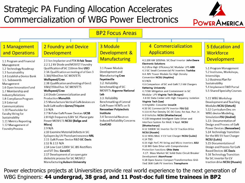
Power electronics projects at Universities provide real world experience to the next generation of WBG Engineers: 44 undergrad, 38 grad, and 11 Post-doc full time trainees in BP2
Strategic PA Funding Allocation Accelerates Commercialization of WBG Power Electronics

PA Member Wolfspeed has a Highly Efficient Vertically Integrated WBG Manufacturing Model
• $171M revenue (FY2016) • 2240 patents worldwide
• 323,000 sq. ft. of fabrication and office facilities • Class 10, 100, and 1000 Clean Rooms

150-mm X-FAB Open SiC Foundry Exploits Existing Si Economy of Scale to Reduce SiC Manufacturing Cost
X-FAB/PowerAmerica Manufacturing Vision: Open SiC Foundry at the Economy Scale of Silicon
X-FAB is open 150-mm SiC Foundry fully integrated within a high volume 150-mm Si fab
• Wafer fabrication dominated by fixed O/H costs (Management, Quality, EHS, IT) • Economies of scale the greatest factor in reducing cost: Use the scale
established in Si to accelerate SiC
X-FAB SiC Users: ABB, GeneSiC, Monolith, USCi, Global Power, and NCSU

0
1
2
3
4
5
6
7
8
9
0 5 10 15
Drain Cu
rren
t (A)
Drain Voltage (V)
Vg=25V
Vg=20V
Vg=15V
Vg=10V
Vg=5V
Vg=0V
Specific on resistance: 5.5 mΩ-cm2 at 1 A, Vg=20V
MOSFET Active area is 4.5 mm2
PowerAmerica process yielded 1.2 kV MOSFETs in its first run
1.00E-‐10
1.00E-‐05
2.00E-‐05
3.00E-‐05
4.00E-‐05
5.00E-‐05
6.00E-‐05
7.00E-‐05
8.00E-‐05
9.00E-‐05
0 500 1000 1500Drain Cu
rren
t (A)
Drain Voltage (V)
PiN
MOSFET (Vgs=0V)1.00E-‐10
1.00E-‐05
2.00E-‐05
3.00E-‐05
4.00E-‐05
5.00E-‐05
6.00E-‐05
7.00E-‐05
8.00E-‐05
9.00E-‐05
0 500 1000 1500
Drain Cu
rren
t (A)
Drain Voltage (V)
PiN
MOSFET (Vgs=0V)
BV 1400V, Id@1200V=1uA
PowerAmerica is developing 3.3, 6.5, and 10 kV MOSFET and JBS Baseline Processes
PowerAmerica has Established Baseline Processes for 1200-V MOSFET and Diode SiC Fabrication at XFAB
PA Processes developed by Prof. Baliga of NCSU and Prof. Sung of SUNY

The PowerAmerica process yielded an integrated 1.2 kV MOSFET/JBS
0
1
2
3
4
5
6
7
8
9
0 5 10 15
Drain Cu
rren
t (A)
Drain Voltage (V)
Vg=25V
Vg=20V
Vg=15V
Vg=10V
Vg=5V
Vg=0V
JBSFET Active area is 4.5 mm2
JBSFET 3rd Q Behavior
PowerAmerica has Established a Baseline Process for 1.2 kV Monolithically Integrated SiC MOS-JBS Fabrication at XFAB
Specific on resistance: 12.5 mΩ-cm2 at 8 A, Vg=20V
PA Processes developed by Prof. Baliga of NCSU and Prof. Sung of SUNY
PowerAmerica is developing 3.3, 6.5, and 10 kV SiC MOS-JBS Baseline Processes

• Interviewed numerous experts in the SiC and GaN communities
• Convened an in-person workshop on June 22, 2016 in Raleigh, North Carolina with +50 attendees
• Held a second virtual workshop with PowerAmerica working group members
• Convened working group meetings to collect additional information and gather feedback on roadmap components
• Reviewed more than 100 sources as part of a background literature review
SiC and GaN Technology Roadmaps Developed Through Expert Interviews and Literature Reviews

SiC Roadmap Identifies Markets & Applications at Each Voltage Node and Outlines Device Performance Requirements
Roadmap tables cover 0.65, 1.2, 1.7, 3.3, 6.5, 10, and 15 kV devices

GaN Roadmap Identifies Markets & Applications at Each Voltage Node and Outlines Device Performance Requirements
Performance Targets Budget Period
2016–2018 2019–2021 2022–2024 2025–2027
Device Type Lateral normally-off switch Lateral normally-off switch Lateral normally-off switch Lateral normally-off switch
Device Cost [$/A]
Device Voltage Rating [V]
Device Rated Current at 25/150oC [A]
Power [kW]
Frequency Range [kHz]
System Efficiency [%]
Packaging Form
Roadmap tables cover devices in the 100-1200 V range
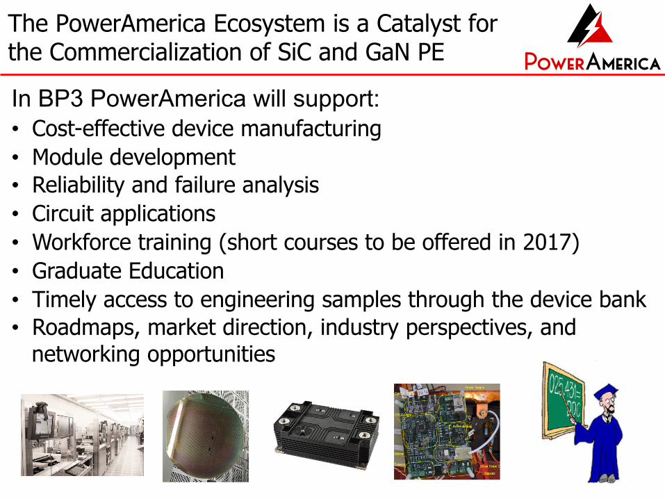
In BP3 PowerAmerica will support: • Cost-effective device manufacturing • Module development • Reliability and failure analysis • Circuit applications • Workforce training (short courses to be offered in 2017) • Graduate Education • Timely access to engineering samples through the device bank • Roadmaps, market direction, industry perspectives, and
networking opportunities
The PowerAmerica Ecosystem is a Catalyst for the Commercialization of SiC and GaN PE