Embed Size (px)
Citation preview

1SNLU237–September 2018Submit Documentation Feedback
Copyright © 2018, Texas Instruments Incorporated
DP83869EVM User's Guide
User's GuideSNLU237–September 2018
DP83869EVM User's Guide
This User’s Guide discusses how to properly operate and configure the DP83869EVM. For best layoutpractices, schematic files, and Bill of Materials, see the associated support documents.

www.ti.com
2 SNLU237–September 2018Submit Documentation Feedback
Copyright © 2018, Texas Instruments Incorporated
DP83869EVM User's Guide
Contents1 Definitions .................................................................................................................... 32 Introduction ................................................................................................................... 43 Board Setup Details ......................................................................................................... 94 Configuration Options ..................................................................................................... 115 Schematics.................................................................................................................. 18
List of Figures
1 DP83869EVM – Top Side .................................................................................................. 52 DP83869EVM – Bottom Side ............................................................................................. 63 Onboard Power Supply Connection ...................................................................................... 74 Jumper Placements for Onboard Power ................................................................................. 75 DP83869EVM Block Diagram.............................................................................................. 96 EVM Strap Jumpers ....................................................................................................... 117 Onboard Clock.............................................................................................................. 158 External Clock Input ....................................................................................................... 159 Schematic Page 1 ......................................................................................................... 1810 Schematic Page 2.......................................................................................................... 1911 Schematic Page 3.......................................................................................................... 2012 Schematic Page 4.......................................................................................................... 2113 Schematic Page 5.......................................................................................................... 2214 Schematic Page 6.......................................................................................................... 23
List of Tables
1 Terminology .................................................................................................................. 32 EVM Applications .......................................................................................................... 103 4 Level Straps .............................................................................................................. 114 2 Level Straps .............................................................................................................. 115 PHY Strap Table ........................................................................................................... 126 Functional Mode Strap Table ............................................................................................. 127 Copper Ethernet Strap Table ............................................................................................. 128 1000Base-X Strap Table .................................................................................................. 139 100Base-X Strap Table.................................................................................................... 1310 Bridge Mode Strap Table.................................................................................................. 1311 100M Media Convertor Strap Table ..................................................................................... 1312 1000M Media Strap Table ................................................................................................ 1413 4-Pin Dip Switch Modes ................................................................................................... 15
TrademarksAll trademarks are the property of their respective owners.

www.ti.com Definitions
3SNLU237–September 2018Submit Documentation Feedback
Copyright © 2018, Texas Instruments Incorporated
DP83869EVM User's Guide
1 Definitions
Table 1. Terminology
ACRONYM DEFINITIONPHY Physical Layer TransceiverMAC Media Access ControllerSMI Serial Management InterfaceMDIO Management Data I/OMDC Management Data ClockMII Media Independent InterfaceRMII Reduced Media Independent InterfaceRGMII Reduced Gigabit Media Independent InterfaceSGMII Serial Gigabit Media Independent InterfaceVDDA Analog Core Supply RailVDDIO Digital Supply RailPD PulldownPU Pullup

Introduction www.ti.com
4 SNLU237–September 2018Submit Documentation Feedback
Copyright © 2018, Texas Instruments Incorporated
DP83869EVM User's Guide
2 IntroductionThe DP83869 is a low power, fully-featured Physical Layer transceiver with integrated PMD sublayers tosupport 10BASE-Te, 100BASE-TX, and 1000BASE-T Ethernet protocols. It also supports Fiber protocols1000BASE-X and 100BASE-FX. Optimized for ESD protection, the DP83869 exceeds 8-kV IEC 61000-4-2(direct contact). This device interfaces to the MAC layer through Reduced GMII (RGMII) and SGMII.Integrated Termination Impedance on RGMII helps reduce system BOM. The DP83869EVM willdemonstrate all features of DP83869. The EVM will support Copper Ethernet protocols like 10BASE-Te,100BASE-TX, and 1000BASE-T. It also supports Fiber protocols 1000BASE-X and 100BASE-FX. TheEVM has connections to use the DP83869 MAC Inerface in RGMII and SGMII mode. The EVM will alsobe optimized to demonstrate the robust EMI. EMC, and ESD performance of the DP83869 device.
2.1 Key Features• Multiple Operating Modes
– Media Support: Copper and Fiber– Media Conversion: Copper to Fiber– Bridge Conversion: RGMII to SGMII, SGMII to RGMII
• RGMII and SGMII MAC Interfaces• 1000Base-X, 100Base-T, 100Base-TX, 10Base-Te• USB-2-MDIO Support Through Onboard MSP430 for Easy Register Access• Onboard LDO and External Power Supply Options• Status LEDs
– Link– Activity– Power
• Bootstraps for Hardware Configuration

www.ti.com Introduction
5SNLU237–September 2018Submit Documentation Feedback
Copyright © 2018, Texas Instruments Incorporated
DP83869EVM User's Guide
Figure 1. DP83869EVM – Top Side

Introduction www.ti.com
6 SNLU237–September 2018Submit Documentation Feedback
Copyright © 2018, Texas Instruments Incorporated
DP83869EVM User's Guide
Figure 2. DP83869EVM – Bottom Side

www.ti.com Introduction
7SNLU237–September 2018Submit Documentation Feedback
Copyright © 2018, Texas Instruments Incorporated
DP83869EVM User's Guide
2.2 Quick Setup
2.2.1 Onboard Power Supply OperationThe EVM can be supplied power through multiple options. Single-supply operation uses onboard LDOs togenerate the voltages required for operating various sections of the EVM (PHY, MSP430, FO transceiver,and so forth).
Figure 3. Onboard Power Supply Connection
The EVM can be supplied power by either a J26 barrel jack connector, power-supply turrets, or a USB• For Barrel Jack and Turret, connect the jumper in the ON position to J22 and the jumper on 5V-LDO to
J34.• For USB power, connect the Jumper on 5V-USB position to J35. J23 is don’t care.
2.2.2 External Power Supply Operation
Figure 4. Jumper Placements for Onboard Power
The jumpers shown in Figure 4 can be used to choose whether a particular voltage rail is supplied throughonboard LDOs or an external power supply. If an external power supply is desired on a voltage rail,change its respective jumper from position 1-2 (LDO) to 2-3 (External). Then connect the appropriatevoltage on its corresponding pin to the P1 connector. For example, if the VDDA2P5 is to be supplied froman external supply, then change jumper position of J36 from 1-2 to 2-3. Then connect the 2.5-V externalsupply on pins 9-10 on the P1 connector. Note that pin 9 is supply and pin 10 is ground.
2.2.3 SoftwareThe onboard MSP430 comes pre-programmed and ready to use. When using this EVM for the first timeon a Windows 7 (or above) PC, MSP430 drivers and USB2MDIO software utility will have to be installed.The USB2MDIO software can be used for accessing registers.
2.2.3.1 MSP430 DriverInstall the latest MSP430 drive from this website: http://software-dl.ti.com/msp430/msp430_public_sw/mcu/msp430/MSP430_FET_Drivers/latest/index_FDS.html.

Introduction www.ti.com
8 SNLU237–September 2018Submit Documentation Feedback
Copyright © 2018, Texas Instruments Incorporated
DP83869EVM User's Guide
2.2.3.2 USB-2-MDIO SoftwareDownload the software from http://www.ti.com/tool/usb-2-mdio. The Web page also contains a User’sGuide for installing and using the software.
The MSP430 is on board the EVM, so it is not required to purchase a separate MSP430 Launchpad kitand connect to the PHY using wires. The entire EVM can be powered and controlled through a USBconnector. MSP430 and USB2MDIO utility can be used even when power is not supplied through a USB.
In case the onboard MSP430 cannot be used due to some reason, MDIO and MDC pins are also brokenout on the J15 connector. Customers can connect a MSP430 launchpad or their own MDIO-MDC utility onJ15 to access the PHY registers.
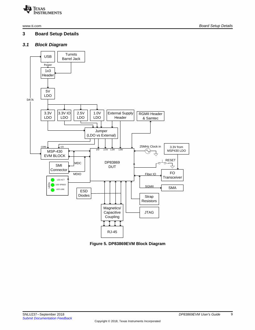
DP83869DUT
5VLDO
1.0VLDO
2.5VLDO
3.3V IOLDO
MSP-430EVM BLOCK
3.3VLDO
LED
s
LED SPEED
LED ACT
LED LINK
SMIConnector
Magnetics/Capacitive Coupling
RJ-45
FOTransceiver
RGMII Header& Samtec
SMA
USB
External Supply Header
25MHz Clock in
MDC
MDIO
SGMII
Fiber IO
ESDDiodes
RESET
TurretsBarrel Jack
3.3V from MSP430 LDO
1x3 Header
Power
DATA
Jumper(LDO vs External)
1.0VI/O 2.5V 1.8V
I/OCORE
Strap Resistors
JTAG
www.ti.com Board Setup Details
9SNLU237–September 2018Submit Documentation Feedback
Copyright © 2018, Texas Instruments Incorporated
DP83869EVM User's Guide
3 Board Setup Details
3.1 Block Diagram
Figure 5. DP83869EVM Block Diagram

Board Setup Details www.ti.com
10 SNLU237–September 2018Submit Documentation Feedback
Copyright © 2018, Texas Instruments Incorporated
DP83869EVM User's Guide
3.2 EVM High-Level SummaryThe DP83869EVM supports SMI through J2 using pin 26 for MDIO and 28 for MDC. These pins can beconnected to an MSP430 Launchpad, which can be used for USB-2-MDIO control.
Table 2. EVM Applications
NO. DP83869 MODE APPLICATIONS HOW TO USE1 RGMII to Copper Run traffic between RGMII and Copper. Connect to DP83867 RGMII EVM or MAC
System using Header pins/Samtech connector.Perform IEEE and UNH compliance testing Use onboard MSP430 to activate test mode
waveform on DP83869Run EMI/EMC Test on EVM Use internal PRBS and loopbackMeasure Power Dissipation Connect external power supplies.External MAC loopback Connect external MAC to headers/Samtech
connector.2 SGMII to Copper Run traffic between SGMII and Copper. Connect to DP83867 SGMII EVM or MAC
System using SMA connector.Perform IEEE and UNH compliance testing Use onboard MSP430 to activate test mode
waveform on DP83869.Run EMI/EMC Test on EVM Use internal PRBS and loopbackExternal SGMII loopback Use SMA cable for Passive Loopback.
3 RGMII to FiberEthernet
Run traffic between RGMII and Fiber Ethernet. Straps to enable Fiber Ethernet. Connect toDP83867 RGMII EVM or MAC System usingHeader/Samtech.
Perform IEEE and UNH compliance testing Use onboard MSP430 to activate test modewaveforms.
Run EMI/EMC Test on EVM Use internal PRBS and loopbackMeasure Power Dissipation Connect external power supplies.
4 100M Media Convertor Demonstrate 100M functionality on EVM Use SFP and RJ45 connector for fiber andcopper ethernet. Straps will be used forunmanaged mode and MDIO for managedmode.
Demonstrate FAR End fault capabilityDemonstrate unmanaged mode of Mediaconvertor
5 1000M MediaConvertor
Demonstrate 1000M functionality on EVM Use SFP and RJ45 connector for fiber andcopper ethernet. Straps will be used forunmanged mode and MDIO for managed mode.Demonstrate Link Loss Pass Thru Capability
Demonstrate unmanaged mode of MediaConvertor
6 RGMII to SGMII bridge Demonstrate SGMII as MAC able to link withSGMII i/f of Phy ( DP83867)
Connect to DP83867 SGMII EVM over SMAconnectors and monitor RGMII header on 869EVM.Demonstrate SGMII link speed is reflected on
RGMIIDemonstrate Complete Data path Use-case Use DP83867 RGMII EVM and SGMII EVM with
DP83869EVM.7 SGMII to RGMII bridge Demonstrate RGMII of DP83869 is able to link-
up with RGMII of DP83867Connect to DP83867 RGMII EVM over Samtechconnectors and monitor SGMII SMA on 869EVM.Demonstrate SGMII link speed is reflecting
RGMII speedDemonstrate Complete Data path Use-case Use DP83867 RGMII EVM and SGMII EVM with
DP83869EVM.

www.ti.com Configuration Options
11SNLU237–September 2018Submit Documentation Feedback
Copyright © 2018, Texas Instruments Incorporated
DP83869EVM User's Guide
4 Configuration Options
4.1 Bootstrap OptionsExcept PHYADD straps, all other straps are only two-level straps in DP83869. EVM will support onepullup and one pulldown resistor pad on RX_D0 and RX_D2 for PHY address straps. There will be onlyone pullup resistor on all other strap pins with an jumper option to disconnect it.
Table 3. 4 Level Straps
STRAP VALUE MODE 1 MODE 2 MODE 3 MODE 4Resistor PU (kΩ) Open 10 5.76 2.49Resistor PD (kΩ) Open 2.49 2.49 Open
Table 4. 2 Level Straps
STRAP VALUE MODE 1 MODE 2Resistor PU (kΩ) 2.49 OpenResistor PD (kΩ) Open 2.49
Figure 6. EVM Strap Jumpers

Configuration Options www.ti.com
12 SNLU237–September 2018Submit Documentation Feedback
Copyright © 2018, Texas Instruments Incorporated
DP83869EVM User's Guide
4.1.1 Straps for PHY Address
Table 5. PHY Strap Table
PIN NAME STRAP NAME PIN NO. DEFAULT
RX_D0 PHY_ADD[1:0] 33 00
PHY_ADD1 PHY_ADD0MODE 0 0 0MODE 1 0 1MODE 2 1 0MODE 3 1 1
RX_D1 PHY_ADD[3:2] 34 00
PHY_ADD3 PHY_ADD2MODE 0 0 0MODE 1 0 1MODE 2 1 0MODE 3 1 1
4.1.2 Strap for DP83869 Functional Mode Selection
Table 6. Functional Mode Strap Table
PIN NAME STRAP NAME PIN NO. DEFAULT OPMODE_2
OPMODE_1
OPMODE_0 FUNCTIONAL MODES
JTAG_TDO/GPIO_1 OPMODE_0 22 0
0 0 0 RGMII to Copper( 1000Base-T/100Base-TX/10Base-Te)
0 0 1 RGMII to 1000Base-X
RX_D3 OPMODE_1 36 00 1 0 RGMII to 100Base-FX0 1 1 RGMII-SGMII Bridge Mode
RX_D2 OPMODE_2 35 0
1 0 0 1000Base-T to 1000Base-X1 0 1 100Base-T to 100Base-FX
1 1 0 SGMII to Copper( 1000Base-T/100Base-TX/10Base-Te)
1 1 1 JTAG for boundary scan
4.1.3 Straps for RGMII/SGMII to Copper
Table 7. Copper Ethernet Strap Table
PIN NAME STRAP NAME PIN NO. DEFAULT
LED_0 ANEG_DIS 47 0
ANEG_DIS
ANEGSEL_1
ANEGSEL_0 FUNCTION
0 0 0 Auto-negotiation, 1000/100/10advertised, Auto MDI-X
0 0 1 Auto-negotiation, 1000/100advertised, Auto MDI-X
LED_1 ANEGSEL_0 46 0
0 1 0 Auto-negotiation, 100/10advertised, Auto-MDI-X
0 1 1 Reserved (JTAG for boundaryscan)
1 0 0 Forced 1000M, master, MDImode

www.ti.com Configuration Options
13SNLU237–September 2018Submit Documentation Feedback
Copyright © 2018, Texas Instruments Incorporated
DP83869EVM User's Guide
Table 7. Copper Ethernet Strap Table (continued)PIN NAME STRAP NAME PIN NO. DEFAULT
LED_2 ANEGSEL_1 45 0
1 0 1 Forced 1000M, slave, MDI mode
1 1 0 Forced 100M, full duplex, MDImode
1 1 1 Forced 100M, full duplex, MDI-Xmode
RX_CTRL MIRROR_EN 38 00 Port Mirroring Disabled1 Port Mirroring Enabled
4.1.4 Straps for RGMII to 1000Base-X
Table 8. 1000Base-X Strap Table
PIN NAME STRAP NAME PIN # DEFAULT
LED_0 ANEG_DIS 47 00 Fiber Auto-negotiation ON1 Fiber Force mode
LED_1 ANEGSEL_0 46 00 Signal Detect disable on Pin 241 Configure Pin 24 as Signal Detect Pin
4.1.5 Straps for RGMII to 100Base-FX
Table 9. 100Base-X Strap Table
PIN NAME STRAP NAME PIN # DEFAULT
LED_1 ANEGSEL_0 46 00 Signal Detect disable on Pin 241 Configure Pin 24 as Signal Detect Pin
4.1.6 Straps for Bridge Mode (SGMII-RGMII)
Table 10. Bridge Mode Strap Table
PIN NAME STRAP NAME PIN # DEFAULT
RX_CTRL MIRROR_EN 38 00 RGMII to SGMII ( RGMII : MAC I/F, SGMII : Phy
I/F)
1 SGMII to RGMII ( SGMII : MAC I/F, RGMII : PhyI/F)
4.1.7 Straps for 100M Media Convertor
Table 11. 100M Media Convertor Strap Table
PIN NAME STRAPNAME PIN # DEFAULT
LED_1 ANEGSEL_0 46 0 ANEGSEL_
1ANEGSEL_
0
LED_2 ANEGSEL_1 45 0
0 0 Copper : Auto-negotiation ( 100/10Advertised), Auto MDIX
1 1 Copper : Auto Negotiation ( 100Advertised), Auto MDIX

Configuration Options www.ti.com
14 SNLU237–September 2018Submit Documentation Feedback
Copyright © 2018, Texas Instruments Incorporated
DP83869EVM User's Guide
Table 11. 100M Media Convertor Strap Table (continued)
PIN NAME STRAPNAME PIN # DEFAULT
RX_CTRL MIRROR_EN 38 0
0 Copper: Mirror Disable1 Copper: Mirror Enable
RX_CLK LINK_LOSS 32 00 Link Loss Pass Thru Enabled1 Link Loss Pass Thru Disabled
4.1.8 Straps for 1000M Media Convertor
Table 12. 1000M Media Strap Table
PIN NAME STRAPNAME PIN # DEFAULT
LED_0 ANEG_DIS 47 00 Fiber Auto Negotiation1 Fiber Force Mode
LED_1 ANEGSEL_0 46 0 ANEGSEL_
1ANEGSEL_0
LED_2 ANEGSEL_1 45 0
0 0 Copper : Auto-negotiation ( 1000/100Advertised), Auto MDIX
1 1 Copper : Auto Negotiation ( 1000Advertised), Auto MDIX
4.2 SGMII/Fiber InterfaceSGMII Pins from the DUT are multipurpose pins functioning as SGMII and Fiber IO pins. By default, theEVM will be configured for Fiber operation.
NOTE: Fiber Transceiver is not a part of the EVM package. SFP cage and SFP connector will bemounted.
For routing signals to Fiber Transceiver, populate R31, R38, R45, and R47. Remove C12, C14, C15, andC17.
For routing signals to SGMII SMAs, populate C12, C14, C15, and C17. Remove R31, R38, R45, and R47.
4.3 RGMIIRGMII signals are routed to standard 2.54-mm header connectors on J14. RGMII can be used both inCopper mode and Fiber mode.
4.4 Clock OutputThe EVM has a SMB connector to output clock from the PHY. A 50-Ω Coax cable with a SMB connectorshould be used for accessing the clock output.
4.5 Clock InputThe EVM is configured for default crystal input clock operation. It supports the option to provide clock from25-MHz crystal, 25-MHz CMOS oscillator, and the External clock from the SMB connector. A 50-Ω Coaxcable with a SMB connector should be used for providing clock input from external sources.

www.ti.com Configuration Options
15SNLU237–September 2018Submit Documentation Feedback
Copyright © 2018, Texas Instruments Incorporated
DP83869EVM User's Guide
Figure 7. Onboard Clock
Figure 8. External Clock Input
4.6 Switch Configuration OptionsThe DP83869EVM includes a 4-pin dip switch (S3), which can be used for various test modes and featuredisplays. Some of the switch settings can also be used with the USB-2-MDIO GUI for additional control.Except for switch mode 15, all switch modes are hard-coded and can be used without USB-2-MDIO or anyother serial com port. Refer to Table 13 for switch configurations and LED outputs. For each switch, PU is1 and PD is 0.
Table 13. 4-Pin Dip Switch Modes
Mode SW[4:1] Feature LED Description LEDD14
LEDD15
LEDD16 USB2MDIO
0 0000 Normal Operation
USB-2-MDIO Active (Flashes very brieflyred during read and green during write)
RedGreen Off Off Yes
Program failed to read PHY register Red Off OffNo
Program failed to write PHY register Green Off Off
1 0001 Test Mode 1 -Droop
Successfully entered Test Mode 1 RedGreen Off Green Yes
Failed to enter Test Mode 1 (FlashingLEDs) Red Red Red No
2 0010Test Mode 2 -Clock Frequency,Master Jitter
Successfully entered Test Mode 2 RedGreen Off Red Yes
Failed to enter Test Mode 2 (FlashingLEDs) Red Red Red No
3 0011 Test Mode 3 -Slave Jitter
Successfully entered Test Mode 3 RedGreen Off Red
Green Yes
Failed to enter Test Mode 3 (FlashingLEDs) Red Red Red No

Configuration Options www.ti.com
16 SNLU237–September 2018Submit Documentation Feedback
Copyright © 2018, Texas Instruments Incorporated
DP83869EVM User's Guide
Table 13. 4-Pin Dip Switch Modes (continued)
Mode SW[4:1] Feature LED Description LEDD14
LEDD15
LEDD16 USB2MDIO
(1) During the loop for Mode 15, USB-2-MDIO is not operational. However, other serial port terminals (that is, PuTTY) can be usedto view real-time data.
4 0100 Test Mode 4 -Distortion
Successfully entered Test Mode 4 RedGreen Green Off Yes
Failed to enter Test Mode 4 (FlashingLEDs) Red Red Red No
5 0101 Test Mode 5Successfully entered Test Mode 5 Red
Green Green Green Yes
Failed to set Test Mode 5 (FlashingLEDs) Red Red Red No
6 0110 Force 100MbpsForce 100-Mbps speed with force MDI Red
Green Green Red Yes
Program failed to program the PHYregisters Off Green Red No
7 0111 Force 10Mbps
Force 10-Mbps speed with force MDIand PRBS on. Off Green Red
NoProgram failed to program the PHYregisters Red Red Red
8 1000 Reverse LoopbackSuccessfully entered Reverse Loopback Red
Green Red Off Yes
Failed to enter Reverse Loopback(Flashing LEDs) Red Red Red No
9 1001 xMII LoopbackSuccessfully entered xMII Loopback Red
Green Red Green Yes
Failed to enter xMII Loopback (FlashingLEDs) Red Red Red No
10 1010 Enable BISTEnable BIST in Copper Ethernet Mode Red Green Red
GreenNo
Program failed to program the PHYregisters Red Red Red
11 - 14 1011 -1110 RESERVED RESERVED - - - No
15 1111
LOOP: Read datacontinuously from alist of registersloaded to the MC
To upload a list of registers tocontinuously read from with USB-2-MDIO: Write the hex value of the registeryou want to add to the list to the registeraddress "LOAD"
RedGreen
RedGreen
RedGreen Yes (1)To begin reading data continuously with
USB-2-MDIO: Read the register address"OPEN"To stop reading data continuously withUSB-2-MDIO: Read the register address"STOP"
When running switch mode 15, data is constantly sent to the serial port. USB-2-MDIO is not capable ofsupporting the constant read feature. However, other serial port terminals, that is, PuTTY, can be used.When using a serial port terminal, copy and paste data. Do not enter in the data slowly, because thefirmware will execute as soon as the data is received.
To load a list of registers to read data from, follow this data format:
##LOADAAAAB/
• ## = Two digit PHY ID expressed in decimal form• LOAD = the string 'LOAD' indicates to the MC to add a register to the list• AAAA = Four character Register Address to read data from in hex form (that is, Read register 0x133h,
set AAAA = 0133)

www.ti.com Configuration Options
17SNLU237–September 2018Submit Documentation Feedback
Copyright © 2018, Texas Instruments Incorporated
DP83869EVM User's Guide
• B = use '*' for an extended access read and '=' for a direct access read• / = end string with '/'
For example, to load register 0x462h with PHY_ID = 1 with extended access, copy and paste the followingcommand into a serial com terminal: 01LOAD0462*/
To start reading data, continuously copy and paste the following into the serial com terminal: OPEN
To stop reading data, continuously copy and paste the following into the serial com terminal: STOP
NOTE: The "OPEN" and "STOP" commands are in no particular position, so the designer can copy"OPENSTOP" and paste it into the serial com terminal once to start reading data and thenpaste it again to stop reading data, for example.
NOTE: When the read loop is stopped, the list of registers to read is cleared.

Schematics www.ti.com
18 SNLU237–September 2018Submit Documentation Feedback
Copyright © 2018, Texas Instruments Incorporated
DP83869EVM User's Guide
5 Schematics
Figure 9. Schematic Page 1

www.ti.com Schematics
19SNLU237–September 2018Submit Documentation Feedback
Copyright © 2018, Texas Instruments Incorporated
DP83869EVM User's Guide
Figure 10. Schematic Page 2
Schematics www.ti.com
20 SNLU237–September 2018Submit Documentation Feedback
Copyright © 2018, Texas Instruments Incorporated
DP83869EVM User's Guide
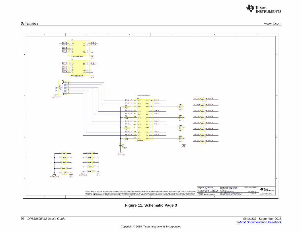
Figure 11. Schematic Page 3

www.ti.com Schematics
21SNLU237–September 2018Submit Documentation Feedback
Copyright © 2018, Texas Instruments Incorporated
DP83869EVM User's Guide
Figure 12. Schematic Page 4

Schematics www.ti.com
22 SNLU237–September 2018Submit Documentation Feedback
Copyright © 2018, Texas Instruments Incorporated
DP83869EVM User's Guide
Figure 13. Schematic Page 5

www.ti.com Schematics
23SNLU237–September 2018Submit Documentation Feedback
Copyright © 2018, Texas Instruments Incorporated
DP83869EVM User's Guide
Figure 14. Schematic Page 6

24 SNLU237–September 2018Submit Documentation Feedback
DP83869EVM User's Guide

www.ti.com Schematics
25SNLU237–September 2018Submit Documentation Feedback
Copyright © 2018, Texas Instruments Incorporated
DP83869EVM User's Guide
IMPORTANT NOTICE AND DISCLAIMER
TI PROVIDES TECHNICAL AND RELIABILITY DATA (INCLUDING DATASHEETS), DESIGN RESOURCES (INCLUDING REFERENCEDESIGNS), APPLICATION OR OTHER DESIGN ADVICE, WEB TOOLS, SAFETY INFORMATION, AND OTHER RESOURCES “AS IS”AND WITH ALL FAULTS, AND DISCLAIMS ALL WARRANTIES, EXPRESS AND IMPLIED, INCLUDING WITHOUT LIMITATION ANYIMPLIED WARRANTIES OF MERCHANTABILITY, FITNESS FOR A PARTICULAR PURPOSE OR NON-INFRINGEMENT OF THIRDPARTY INTELLECTUAL PROPERTY RIGHTS.These resources are intended for skilled developers designing with TI products. You are solely responsible for (1) selecting the appropriateTI products for your application, (2) designing, validating and testing your application, and (3) ensuring your application meets applicablestandards, and any other safety, security, or other requirements. These resources are subject to change without notice. TI grants youpermission to use these resources only for development of an application that uses the TI products described in the resource. Otherreproduction and display of these resources is prohibited. No license is granted to any other TI intellectual property right or to any thirdparty intellectual property right. TI disclaims responsibility for, and you will fully indemnify TI and its representatives against, any claims,damages, costs, losses, and liabilities arising out of your use of these resources.TI’s products are provided subject to TI’s Terms of Sale (www.ti.com/legal/termsofsale.html) or other applicable terms available either onti.com or provided in conjunction with such TI products. TI’s provision of these resources does not expand or otherwise alter TI’s applicablewarranties or warranty disclaimers for TI products.
Mailing Address: Texas Instruments, Post Office Box 655303, Dallas, Texas 75265Copyright © 2018, Texas Instruments Incorporated