Embed Size (px)
Citation preview

Dot-MatrixLCD Units(with built-in controllers)
DISPLAY UNIT USER’S MANUAL
LIFE SUPPORT POLICY
SHARP components should not be used in medical devices with life support functions or in safety equipment (or similiarapplications where component failure would result in loss of life or physical harm) without the written approval of anofficer of the SHARP Corporation.
LIMITED WARRANTY
SHARP warrants to its Customer that the Products will be free from defects in material and workmanship under normaluse and service for a period of one year from the date of invoice. Customer’s exclusive remedy for breach of this warrantyis that SHARP will either (i) repair or replace, at its option, any Product which fails during the warranty period becauseof such defect (if Customer promptly reported the failure to SHARP in writing) or, (ii) if SHARP is unable to repair orreplace, refund the purchase price of the Product upon its return to SHARP. This warranty does not apply to any Productwhich has been subjected to misuse, abnormal service or handling, or which has been altered or modified in design orconstruction, or which has been serviced or repaired by anyone other than Sharp. The warranties set forth herein are inlieu of, and exclusive of, all other warranties, express or implied. ALL EXPRESS AND IMPLIED WARRANTIES,INCLUDING THE WARRANTIES OF MERCHANTABILITY, FITNESS FOR USE AND FITNESS FOR A PARTICULARPURPOSE, ARE SPECIFICALLY EXCLUDED. In no event will Sharp be liable, or in any way responsible, for anyincidental or consequential economic or property damage.
The above warranty is also extended to Customers of Sharp authorized distributors with the following exception: reportsof failures of Products during the warranty period and return of Products that were purchased from an authorizeddistributor must be made through the distributor. In case Sharp is unable to repair or replace such Products, refunds willbe issued to the distributor in the amount of distributor cost.
SHARP reserves the right to make changes in specifications at any time and without notice. SHARP does not assumeany responsibility for the use of any circuitry described; no circuit patent licenses are implied.
© 1999 SHARP Microelectronics of the Americas Printed in the USA.
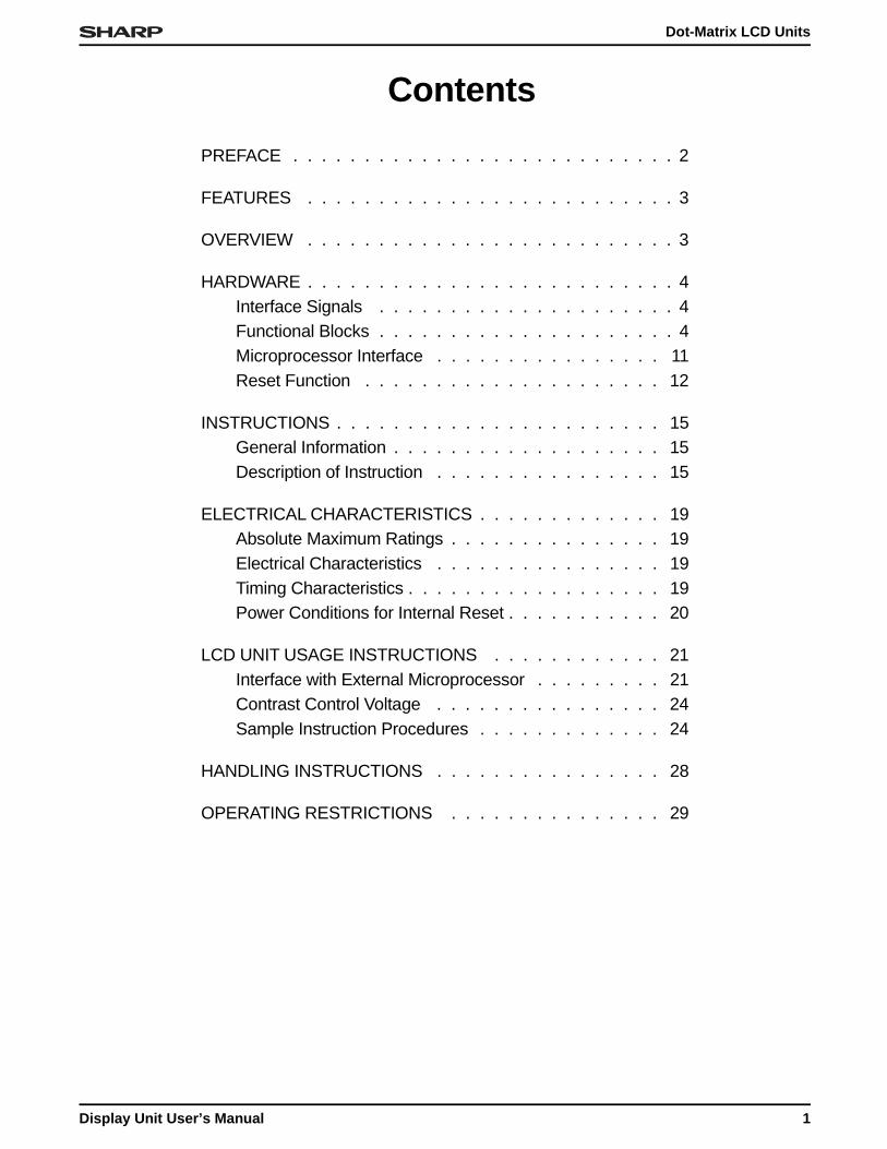
Contents
PREFACE . . . . . . . . . . . . . . . . . . . . . . . . . . . 2
FEATURES . . . . . . . . . . . . . . . . . . . . . . . . . . 3
OVERVIEW . . . . . . . . . . . . . . . . . . . . . . . . . . 3
HARDWARE . . . . . . . . . . . . . . . . . . . . . . . . . . 4Interface Signals . . . . . . . . . . . . . . . . . . . . . 4Functional Blocks . . . . . . . . . . . . . . . . . . . . . 4Microprocessor Interface . . . . . . . . . . . . . . . . 11Reset Function . . . . . . . . . . . . . . . . . . . . . 12
INSTRUCTIONS . . . . . . . . . . . . . . . . . . . . . . . 15General Information . . . . . . . . . . . . . . . . . . . 15Description of Instruction . . . . . . . . . . . . . . . . 15
ELECTRICAL CHARACTERISTICS . . . . . . . . . . . . . 19Absolute Maximum Ratings . . . . . . . . . . . . . . . 19Electrical Characteristics . . . . . . . . . . . . . . . . 19Timing Characteristics . . . . . . . . . . . . . . . . . . 19Power Conditions for Internal Reset . . . . . . . . . . . 20
LCD UNIT USAGE INSTRUCTIONS . . . . . . . . . . . . 21Interface with External Microprocessor . . . . . . . . . 21Contrast Control Voltage . . . . . . . . . . . . . . . . 24Sample Instruction Procedures . . . . . . . . . . . . . 24
HANDLING INSTRUCTIONS . . . . . . . . . . . . . . . . 28
OPERATING RESTRICTIONS . . . . . . . . . . . . . . . 29
Dot-Matrix LCD Units
Display Unit User’s Manual 1
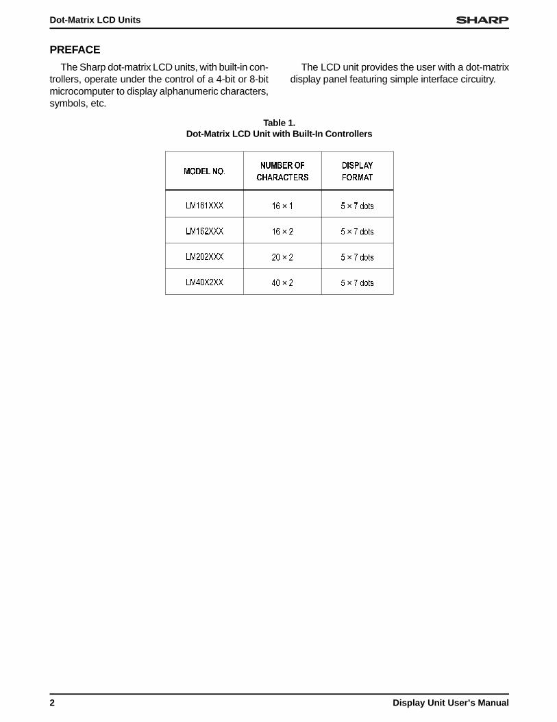
PREFACE
The Sharp dot-matrix LCD units, with built-in con-trollers, operate under the control of a 4-bit or 8-bitmicrocomputer to display alphanumeric characters,symbols, etc.
The LCD unit provides the user with a dot-matrixdisplay panel featuring simple interface circuitry.
02'(/ 12180%(5 2)
&+$5$&7(56
',63/$<
)250$7
/0;;; × × GRWV
/0;;; × × GRWV
/0;;; × × GRWV
/0;;; × × GRWV
Table 1.Dot-Matrix LCD Unit with Built-In Controllers
Dot-Matrix LCD Units
2 Display Unit User’s Manual

FEATURES• Interface with either 4-bit or 8-bit
microprocessor.
• Display data RAM
• 80 × 8 bits (80 characters).
• Character generator ROM
• 160 different 5 × 7 dot-matrix characterpatterns.
• Character generator RAM
• 8 different user programmed 5 × 7dot-matrix patterns.
• Display data RAM and character generatorRAM may be accessed by themicroprocessor.
• Numerous instructions
• Clear Display, Cursor Home, DisplayON/OFF, Cursor ON/OFF, Blink Character,Cursor Shift, Display Shift.
• Built-in reset circuit is triggered at powerON.
• Built-in oscillator.
OVERVIEWThe LCD unit receives character codes (8 bits per
character) from a microprocessor or microcomputer,latches the codes to its display data RAM (80-byteDD RAM for storing 80 characters), transforms eachcharacter code into a 5 × 7 dot-matrix characterpattern, and displays the characters on its LCDscreen.
The LCD unit incorporates a character generatorROM which produces 160 different 5 × 7 dot-matrixcharacter patterns. The unit also provides a char-acter generator RAM (64 bytes) through which theuser may define up to eight additional 5 × 7 dot-ma-trix character patterns, as required by the applica-tion.
To display a character, positional data is sent viathe data bus from the microprocessor to the LCDunit, where it is written into the instruction register.A character code is then sent and written into thedata register. The LCD unit displays the correspond-ing character pattern in the specified position. TheLCD unit can either increment or decrement thedisplay position automatically after each characterentry, so that only successive characters codesneed to be entered to display a continuous characterstring. The display/cursor shift instruction allows theentry of characters in either the left-to-right or right-to-left direction. Since the display data RAM (DDRAM) and the character generator RAM (CG RAM)many be accessed by the microprocessor, unusedportions of each RAM may be used as generalpurpose data areas. The LCD unit may be operatedwith either dual 4-bit or single 8-bit data transers, toaccommodate interfaces with both 4-bit and 8-bitmicroprocessors. The low power feature of the LCDunit will be further appreciated when combined witha CMOS microprocessor.
Dot-Matrix LCD Units
Display Unit User’s Manual 3

HARDWARE
Interface Signals
Functional Blocks
Registers
The LCD unit has two 8-bit registers - an instruc-tion register (IR) and a data register (DR). Theinstruction register stores instruction codes such as"clear display" or "shift cursor", and also storesaddress information for the display data RAM andcharacter generator RAM. The IR can be accessedby the microprocessor only for writing.
The data register is used for temporarily storingdata during data transactions with the microproces-sor. When writing data to the LCD unit, the data isinitially stored in the data register, and is then auto-matically written into either the display data RAM orcharacter generator RAM, as determined by the
current operation. The data register is also used asa temporary storage area when reading data fromthe display data RAM or character generator RAM.When address information is written into the instruc-tion register, the corresponding data from the displaydata RAM or character generator RAM is moved tothe data register. Data transfer is completed whenthe microprocessor reads the contents of the dataregister by the next instruction. After the transfer iscompleted, data from the next address position ofthe appropriate RAM is moved to the data register,in preparation for subsequent reading operations bythe microprocessor. One of the two registers isselected by the register select (RS) signal.
6,*1$/ 1$0( ,1387287387(;7(51$/
&211(&7,21)81&7,21
56 ,QSXW 038 5HJLVWHU VHOHFW VLJQDO
,QVWUXFWLRQ UHJLVWHU ZKHQ ZULWLQJ
%XV\ IODJ DQG DGGUHVV FRXQWHU ZKHQ UHDGLQJ
'DWD UHJLVWHU ZKHQ ZULWLQJ DQG UHDGLQJ
5: ,QSXW 038 5HDGZULWH VHOHFW VLJQDO :ULWLQJ 5HDGLQJ
( ,QSXW 038 2SHUDWLRQ GDWD UHDGZULWH HQDEOH VLJQDO
'% '% ,QSXW2XWSXW 038 +LJKRUGHU OLQHV RI GDWD EXV ZLWK WKUHHVWDWH ELGLUFWLRQDO IXQFWLRQ IRU XVH LQ GDWD
WUDQVDFWLRQV ZLWK WKH 038 '% PD\ DOVR EH XVHG WR FKHFN WKH EXV\ IODJ
'% '% ,QSXW2XWSXW 038 /RZRUGHU OLQHV RI GDWD EXV ZLWK WKUHHVWDWH ELGLUHFWLRQDO IXQFWLRQ IRU XVH LQ GDWD
WUDQVDFWLRQV ZLWK WKH 038
7KHVH OLQHV DUH QRW XVHG ZKHQ LQWHUIDFLQJ ZLWK D ELW PLFURSURFHVVRU
9'' 966 3RZHU 6XSSO\ 9'' 9 966 *1'
9 3RZHU 6XSSO\ &RQWUDVW DGMXVWPHQW YROWDJH
Table 2. Interface Signals
56 5: 23(5$7,21
:ULWH WR LQVWUXFWLRQ UHJLVWHU DQG H[HFXWH LQWHUQDO RSHUDWLRQ FOHDU GLVSOD\ HWF
5HDG EXV\ IODJ '% DQG DGGUHVV FRXQWHU '% '%
:ULWH WR GDWD UHJLVWHU DQG H[HFXWH LQWHUQDO RSHUDWLRQ '5→ '' 5$0 RU '5 → &* 5$0
5HDG GDWD UHJLVWHU DQG H[HFXWH LQWHUQDO RSHUDWLRQ '' 5$0→ '5 RU &* 5$0 → '5
Table 3. Register Selection
Dot-Matrix LCD Units
4 Display Unit User’s Manual

Busy Flag (BF)
When the busy flag is set at a logical "1", the LCDunit is executing an internal operation, and no in-struction will be accepted. The state of the busy flagis output on data line DB7 in response to the registerselection signals RS = 0, R/W = 1 as shown in Table3. The next instruction may be entered after thebusy flag is reset to logical "0".
Address Counter (AC)
The address counter generates the address forthe display data RAM and character generatorRAM. When the address set instruction is writteninto the instruction register, the address informationis sent to the address counter. The same instrucitonalso determines which of the two RAM’s is to beselected.
After data has been written to or read from thedisplay data RAM or character generator RAM, theaddress counter is automatically incremented ordecremented by one. The contents of the addresscounter are output on data lines DB0 - DB6 inresponse to the register selection signals RS = 0,R/W = 1 as shown in Table 3.
Display Data RAM (DD RAM)
This 80 x 8 bit RAM stores up to 80 8-bit charactercodes as display data. The unused area of the RAMmay be used by the microprocessor as a generalpurpose RAM area.
The display data RAM address, set in the addresscounter, is expressed in hexadecimal (HEX) num-bers as follows:
The address of the display data RAM corre-sponds to the display position on the LCD panel asfollows:
a. Address type a . . . .For dual-line display
When a display shift takes place, the addressesshift is as follows:
The addresses for the second line are not con-tinuous to the addresses for the first line. A 40-char-acter RAM area is assigned to each of the two lineas follows:
line 1: 00H - 27H
line 2: 40H - 67H
For an LCD unit with a display capacity of lessthan 40 characters per line, characters equal innumber to the display capacity, as counted fromdisplay position 1, are displayed.
b. Address type b . . . .For single-line display withlogically dual-line addressing
When a display shift takes place, the addressesshift as follows:
The right-hand eight characters, for the purposesof addressing and shifting, may be considered toconstitute a second display line. For the addresstype of each model, see Table 12.
AC6 AC5 AC4 AC3 AC2 AC1 AC0
HEXDigit
AC
High-orderBits
Lower-orderBits
HEXDigit
1
Example: DD RAM address '4E'
0 0 1 1 1 0
4 E
987654321 39 40Display Position
DD RAM Address (HEX)
Digit
Line 1
Line 2
00H 01H 02H 03H 04H 05H 06H 07H 08H 26H 27H
40H 41H 42H 43H 44H 45H 46H 47H 48H 66H 67H
. . .
. . .
LeftShift
01H 02H 03H 04H 05H 06H 07H 08H 09H 27H 00H
41H 42H 43H 44H 45H 46H 47H 48H 49H 67H 40H
. . .
. . .
RightShift
27H 00H 01H 02H 03H 04H 05H 06H 07H 25H 26H
67H 40H 41H 42H 43H 44H 45H 46H 47H 65H 66H
. . .
. . .
161514
Display PositionDigit
Line1
DD RAM Address (HEX)
13121110987654321
00H 47H46H45H44H43H42H41H40H07H06H05H04H03H02H01H
LeftShift
01H 48H47H46H45H44H43H42H41H08H07H06H05H04H03H02H
RightShift
27H 46H45H44H43H42H41H40H67H06H05H04H03H02H01H00H
Dot-Matrix LCD Units
Display Unit User’s Manual 5

Character Generator ROM (CG ROM)
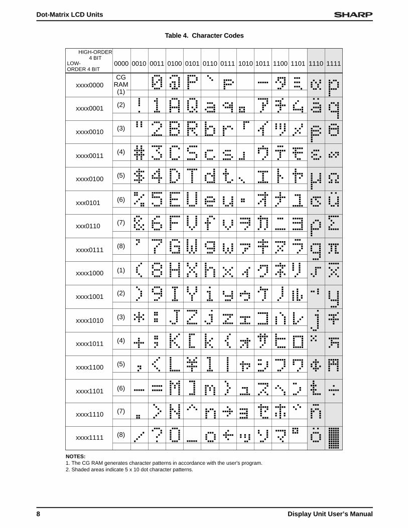
This ROM generates a 5 × 7 dot-matrix characterpattern for each of 160 different 8-bit charactercodes. The correspondence between charactercodes and character patterns is shown in Tables 4and 5. Inquiries are invited for units with customcharacter patterns.
Character Generator RAM (CG RAM)
This RAM stores eight arbitrary 5 x 7 dot-matrixcharacter patterns, as programmed by the user. Fordisplaying a character pattern stored in the CGRAM, a character code corresponding to the left-most column in Tables 4 and 5 is written into thedisplay data RAM.
For the relationship among the CG RAM address,the display data, and the displayed pattern, seeTable 6. As shown in Table 6., the unused portionof the CG RAM may be used as a general purposeRAM area.
Timing Generator
The timing generator produces timing signalsused for the internal operation of the display dataRAM, character generator ROM,and character gen-erator RAM. Timing in controlled so that read-out ofthe RAM for display and access to the RAM by theexternal microprocessor do not interfere. Displayflicker when data is written to the display data RAMis eliminated.
Cursor/Blink Controller
This circuit can be used to generate a cursor orblink a character in the display position indicated bythe DD RAM address, which is set in the addresscounter (AC). The following example shows thecursor position when the address counter contains"08" (HEX).
Parallel-to-Serial Converter
This circuit converts parallel data read from theCG ROM or CG RAM to serial data for use by thedisplay driver.
Bias Voltage Generator
This circuit provides the bias voltage level re-quired for driving the liquid crystal display. Somemodels incorporate a temperature compensationcircuit which generates a temperature dependentbias voltage in order to provide constant displaycontrast at all ambient temperature levels.
LCD Driver
This circuit receives display data, timing signals,and bias voltage, and produces the common andsegment display signals.
LCD Panel
This is a dot-matix liquid crystal display panelarranged in either 1 row of 16 characters, 2 rows of16 characters, 2 rows of 20 characters, or 2 rows of40 characters.
AC 0001000
AC6 AC0AC1AC2AC3AC4AC5
Digit
Line 1
Line 2
Display Position
DD RAMAddress (HEX)
DD RAMAddress (HEX)
Cursor Position
Cursor Position
Single-LineDisplay
1110987654321
00 0A090807060504030201
DigitDisplay Position
Dual-LineDisplay
NOTE:The address counter has the dual function of containing eithera DD RAM address or a CG RAM address. The cursor/blinkcontroller does not distinguish between these two functions,and thus, when activated, it always considers the addresscounter to contain a DD RAM address. To avoid spuriouscursor/blink effects, the cursor/blink function should be turnedoff while the microprocessor writes to or reads from the CG RAM.
1110987654321
00 0A090807060504030201
40 4A494847464544434241
Dot-Matrix LCD Units
6 Display Unit User’s Manual

LCDPanel
CommonElectrode
DriveCircuit
SegmentElectrode
DriveCircuit
DisplayData
Signals 4
ScanningSignals 3
LEDback-light
VLED VLSS
4
ELback-
light
ELInverter
(See note 2)5 V
TimingGenerator
Cursor/BlinkController
33
7
7
7
Display DataRAM
(DD RAM)80 x 8 bits
AddressCounter
(AC)
7
7
7
InstructionDecoder
InstructionRegister (/R)
8
CharacterGenerator
ROM(CG ROM)7,200 bits
8
8
CharacterGenerator
ROM(CG ROM)
512 bits
7
8
Parallel-to-SerialConverter
5
5
Bias Voltage
Generator(See Note 1)
6
Data Register(DR)
8
I/O Buffer
8
BusyFlag (BF)
7
8
RS R/W E
4 4
DB4 - DB7 DB0 - DB3
VDD VO VSS
LCD27-6
NOTES:1. LM16152 incorporates a temperature compensation circuit within the bias voltage generator. See table 12.2. For the inverters of EL backlights, please contact your representative.
Figure 1. Functional Block Diagram
Dot-Matrix LCD Units
Display Unit User’s Manual 7
0000
HIGH-ORDER4 BIT
LOW-ORDER 4 BIT
0010 0011 0100 0101 0110 0111 1010 1011 1100 1101 1110 1111
xxxx0000
xxxx0001
xxxx0010
xxxx0011
xxxx0100
xxx0101
xxx0110
xxxx0111
xxxx1000
xxxx1001
xxxx1010
xxxx1011
xxxx1100
xxxx1101
xxxx1110
xxxx1111
CGRAM(1)
(2)
(3)
(4)
(5)
(6)
(7)
(8)
(1)
(2)
(3)
(4)
(5)
(6)
(7)
(8)
NOTES: 1. The CG RAM generates character patterns in accordance with the user's program.2. Shaded areas indicate 5 x 10 dot character patterns.
Table 4. Character Codes
Dot-Matrix LCD Units
8 Display Unit User’s Manual
High-Order
CGRAM(1)
(3)
(4)
(5)
(6)
(7)
(8)
(1)
(2)
(3)
(4)
(6)
(7)
(8)
××××0000
××××0001
××××0010
××××0011
××××0100
××××0101
××××0110
××××0111
××××1000
××××1001
××××1010
××××1011
××××1100
××××1101
××××1110
××××1111
0000
0 @ P \ p
1! A Q a q
α p
ä q
2" B R b r
3# C S c s
4$ D T d t
5% E U e u
6& F V f v
7’ G W g w
8( H X h x
9) I Y i y
:* J Z j z
;+ K [ k
β θ
ε ∞
µ Ω
σ ü
ρ Σ
π
√ x
_1 y
j
x
¢
£ ÷
n
ö
0010 0011 0100 0101 0110 0111 1010 1011 1100 1101 1110 1111Low-Order 4 bit
(2)
(5) <’
L ¥ 1 |
=- M ] m
>. N ^ n →
?/ O _ o ←
4 bit
Table 5. Character Codes
Dot-Matrix LCD Units
Display Unit User’s Manual 9

Character Code(DD RAM Data) CG RAM Address
Character Pattern(CG RAM Data)
SampleCharacterPattern(1)
Cursor Position
SampleCharacterPattern(2)
7
High-orderbit
Low-orderbit
6 5 4 3 2 1 0
0 0 0 0 1 10 0 0 0 * 0 0 0
0 0 0 1 1 01* *
*
*
* *
1
0 0 1
0 1 0
1 0 0
1 0 1
1 1 1
1 1 0
0 0 1 0 1 1
0 0 0
0 0 1
0 1 0
1 0 0
1 0 1
1 1 1
1 1 0
1 1 1
1 0 0
1 0 1
1 1 1
1 1 0
0 0 1
0 0 0
0 0 0 0 * 0 0 1
0 0 0 0 * 1 1 1
High-orderbit
Low-orderbit
5 4 3 2 1 0 7
High-orderbit
Low-orderbit
6 5 4 3 2 1 0
0 0 11 0
0 0 11 0
1 0 01 0
0 1 01 0
0 0 11 0
0 0 00 0
1 1 01 1
0 0 1* 1* *
** *
** *
** *
0
0 1 00 1
1 1 11 1
1 1 11 1
1 0 00 0
1 0 00 0
0 0 00 0
1 0 00 0
NOTES:1. Character code bits 0 - 2 correspond to CG RAM address bits 3 - 5. Each of the 8 unique bit strings designates one of the 8 character patterns.2. CG RAM address bits 0 - 2 designate the row position of each character pattern. The 8th row is the cursor position. CG RAM data in the 8th row is OR'ed with the display cursor. Any '1' bits in the 8th row will result in a displayed dot regardless of the cursor status (ON/OFF). Accordingly, if the cursor is to be used, CG RAM data for the 8th row should be set to '0'.3. CG RAM data bits 0 - 4 correspond to the column position of each character pattern bit 4 corresponding to the left most column of the character pattern. CG RAM data bits 5 - 7 are not used for displaying character patterns, but may be used as a general purpose RAM area.
4. As shown in tables 4 and 5, character patterns in the CG RAM are accessed by character codes with bits 4 - 7 equal to '0'. For example, the character pattern 'R', shown in the first sample character pattern of the table, is selected by the character code '00' (HEX) or '08' (HEX), since bit 3 of the character code is a don't care" bit (i.e., can take either value, '00' or '1').5. CG RAM data '1' produces a dark dot, and data '0' produces a light dot in the corresponding position on the display panel.6. * = Signifies a "don't care" bit
LCD27-8
Table 6. Relationship Among Character Code(DD RAM), CG RAM Address, and Character Pattern (CG RAM)
Dot-Matrix LCD Units
10 Display Unit User’s Manual

Microprocessor InterfaceThe LCD unit performs either dual 4-bit or single
8-bit data transers, allowing the user to interface witheither a 4-bit or 8-bit microprocessor
4-Bit Microprocessor Interface.
Data lines DB4 - DB7 are used for data transfers.Data transactions with the external microprocessortake place in two 4-bit data transfer operations.
The high-order 4 bits (corresponding to DB4 - DB7in an 8-bit transfer) are transferred first, followed bythe low-order 4 bits (corresponding to DB0 - DB3 inan 8-bit transfer). The busy flag is to be checked oncompletion of the second 4-bit data transfer. Busyflag and address counter are output in two opera-tions.
8-bit Microprocessor InterfaceEach 8-bit piece of data is transferred in a single opera-tion using the entire data bus DB0 - DB7.
IR7DB7
DB6
DB5
DB4
RS
R/W
E
IR3 AC3 DR7 DR3BF
IR6 IR2 AC2 DR6 DR2AC6
IR5 IR1 AC1 DR5 DR1AC5
IR4 IR0 AC0 DR4 DR0AC4
Write toInstruction
Register (IR)
Read BusyFlag (BF) and
AddressCounter (AC)
Read DataRegister (DR)
LCD27-9
Figure 2. 4-Bit Data Transfer
Dot-Matrix LCD Units
Display Unit User’s Manual 11

Reset Function
Initialization by Internal Reset Circuit
The LCD unit has an internal reset circuit forimplementing an automatic reset operation atpower-on. During the initalization operation, thebusy flag is set. The busy state lasts for 10 msecafter VDD reaches 4.5 V. The following instructionsare executed in initializing the LCD unit.
1. Clear Display
2. Function Set
DL = 1 . . . . 8-bit data length for interfaceN = 0 . . . . Single-line displayF = 0 . . . . 5 × 7 dot-matrix character font
3. Display ON/OFF Control
D = 0 . . . .Display OFFC = 0 . . . .Cursor OFFB = 0 . . . .Blink function OFF
4. Entry Mode Set
I/D = 1 . . . .Increment ModeS = 0 . . . .Display shift OFF
CAUTIONIf the power conditions stated in Table 11, "Power condi-tions applicable when internal reset circuit is used," arenot satisfied, then internal reset circuit will not operateproperly and the LCD unit will not be initalized. In thiscase, the initialization procedure must be executed by theexternal microprocessor.
Dot-Matrix LCD Units
12 Display Unit User’s Manual

Initialization by Instructions
If the power conditions for the normal operationof the internal reset circuit are not satisfied (seeTable 11), then LCD unit must be initialized byexecuting a series of instructions. The procedurefor this initialization process is as follows:
Power ON
Wait 15 ms or moreafter VDD reaches 4.5 V
RS R/W DB7 DB6 DB5 DB4 DB3 DB2 DB1 DB0
0 0 0 0 1 1 * * * *
Wait 4.1 ms or more
RS R/W DB7 DB6 DB5 DB4 DB3 DB2 DB1 DB0
0 0 0 0 1 1 * * * *
Wait 100 µs or more
End of Initialization
RS R/W DB7 DB6 DB5 DB4 DB3 DB2 DB1 DB0
0 0 0 0 1 1 * * * *
RS R/W DB7 DB6 DB5 DB4 DB3 DB2 DB1 DB0
0 0 0 0 1 1 N F * *
0 0 0 0 0 0 1 0 0 0
0 0 0 0 0 0 0 0 0 1
0 0 0 0 0 0 0 1 I/D S
Busy flag can't be checked before execution of thisinstruction
Function Set (8-Bit Interface)
Busy flag can't be checked before execution of thisinstruction
Function Set (8-Bit Interface)
Busy flag can't be checked before execution of thisinstruction
Function Set (8-Bit Interface)
(a) Busy flag can be checked after the following instructionsare completed. If the busy flag is not going to be checked,then a wait time longer than the total execution time ofthese instructions is required (See Table 7.)
Function Set
Display Off
Display Clear
Entry Mode Set
8-Bit Interface,Single/Dual LineDisplay, Display Font
Caution: At this point,the display formatan't be changed.
LCD21-10
Figure 3. 8-Bit Interface
Dot-Matrix LCD Units
Display Unit User’s Manual 13

4-Bit Interface
Power ON
Wait 15 ms or moreafter VDD reaches 4.5 V
RS R/W DB7 DB6 DB5 DB4
0 0 0 0 1 1
Wait 4.1 ms or more
RS R/W DB7 DB6 DB5 DB4
0 0 0 0 1 1
RS R/W DB7 DB6 DB5 DB4
0 0 0 0 1 1
RS R/W DB7 DB6 DB5 DB4
0 0 0 0 1 0
0 0 0 0 1 0
0 0 N F * *
Wait 100 µs or more
End of Initialization
Busy flag can't be checked before execution of thisinstruction
Function Set (8-Bit Interface)
Busy flag can't be checked before execution of thisinstruction
Function Set (8-Bit Interface)
Busy flag can't be checked before execution of thisinstruction
Function Set (8-Bit Interface)
(a) Busy flag can be checked after the following instructionsare completed. If the busy flag is not going to be checked,then a wait time longer than the total execution time ofthese instructions is required (See Table 7.)
This instruction signals the LCD unit to begin accepting andsending data in dual 4-bit transfers for all subsequenttransfers for all subsequent transactions. This is the only4-bit instruction recognized by the LCD unit.
II Function Set
III Display Off
IV Display Clear
V Entry Mode Set
4-Bit Interface,Single/Dual LineDisplay, Display Font
LCD21-11
0 0 0 0 0 0
0 0 1 0 0 0
0 0 0 0 0 O
0 0 0 0 0 1
0 0 0 0 0 0
0 0 0 1 I/D S
I Function Set (4-Bit Interface)I
II
III
IV
V
Caution: At this point,the display formatcan't be changed.
Figure 4. 4-Bit Interface
Dot-Matrix LCD Units
14 Display Unit User’s Manual

INSTRUCTIONS
General InformationWhen the LCD unit is controlled by an external
microprocessor, the only registers which can bedirectly accessed by the microprocessor are theinstruction register (IR) and data register (DR). Con-trol information is buffered to allow the LCD unit tointerface with various microprocessors and periph-eral control devices with different operating speeds.The internal operation of the LCD unit is determinedby the signals sent from the external microproces-sor. These signals include the register select (RS)signal, the read/write (R/W) signal, and the data bus(DB0 - DB7) signals.
Table 7 lists the instructions available to the LCDunit, with their execution times. The instructions fallinto the following four categories.
1. Instructions for setting LCD unit functions, suchas display format and data length
2. Instructions for addressing the internal RAM’s
3. Instructions for transferring data to or from theinternal RAM’s
4. Other instructions
In normal operation, instructions from category(3) are used most frequently. The internal RAMaddress may be incremented or decremented auto-matically after each data transaction, to reduce theprogramming requirements of the microprocessor.The display may also be shifted automatically aftereach display data write (see Sample InstructionProcedures section for examples). These featuresfacilitate the construction of efficient systems.
During the internal execution of an instruction, noinstruction other than the "busy flag/address counterread" instruction will be accepted. During internaloperation the busy flag is set to "1". It is necessaryfor the microprocessor to check that the busy flag isreset to "0" before sending the next instruction.
NOTEEither the microprocessor must check that the busy flagis not set to "1" before sending each instruction, or theinterval waited before sending each instruction must bemade sufficiently longer than the execution time of theprevious instruction. For the execution time of eachinstruction, see Table 7.
Description of Instruction
Display Clear
The display data RAM is filled with the "space"code, 20H. The address counter is reset to zero. Ifthe display has been shifted, the original position isrestored. By execution of this instruction, the dis-play goes off, and the cursor and character blinkfunctions, if activated, are moved to the upper, left-most display position.
Display/Cursor Home
The address counter is reset to zero. If the dis-play has been shifted, the original position is re-stored. The content of the DD RAM is not affected.The cursor and character blink functions, if acti-vated, are moved to the upper, leftmost displayposition.
Entry Mode Set
I/D: The address counter is incremented (I/D = 1) ordecremented (I/D = 0) by one, following thereading or writing of each display data RAMcharacter code. The cursor and character blinkfunctions move one display position to the right(I/D = 1) or left (I/D = 0). The same operationtakes place when data is written to or read fromthe character generator RAM.
S: When S = 1, the entire display is shifted oneposition to the left (I/D = 1) or right (I/D = 0)following the writing of a display data RAMcharacter code. The cursor and character blinkfunctions do not move relative to the displayposition. When S = 0, the display is not shifted.The display is not shifted when writing data tothe character generator RAM.
DB0DB7RS R/W
0CODE 0 0 0 0 0 0 0 0 1
DB0DB7RS R/W
0CODE
NOTE: * = Don't Care
0 0 0 0 0 0 0 1 *
DB0DB7RS R/W
0CODE 0 0 0 0 0 0 0 I/D S
Dot-Matrix LCD Units
Display Unit User’s Manual 15

Display ON/OFF
D: When D = 1, the display is turned on.
When D = 0, the display is turned off with thedisplay data retained in the display data RAM.
C: When C = 1, the cursor is displayed in theposition specified by the address counter. WhenC = 0, the cursor is not displayed. The cursor ismade up of five dots displayed across the 8thdisplay row, below the 5 × 7 dot-matrix characterblock. For 5 × 10 dot-matrix character blocks, 5dots are displayed across the 11th row.
B: When B = 1, the character at the cursor positionblinks on and off. When this function is acti-vated, at fcp or fosc = 250 kHz, alternatingbetween all dots black, and the display charac-ter, the character is alternately displayed for409.6 ms and blanked for 409.6 ms. The cursormay be used simultaneously with the characterblink function. (Blink frequency varies in propor-tion to the reciprocal of fCP or fOSC.409.6 × 250/270 = 379.2 ms; fCP = 270 kHz.)
Display/Cursor Shift
The display and/or cursor are shifted to the rightor left. For two-line displays, the cursor moves fromthe 40th position of the top line to the first position ofthe second line. From the 40th position of thesecond line, the cursor does not move back to thehome position, but rather to the first position of thesecond line.
NOTE: When the display is shifted, the address counter isnot affected.
Function Set
DL: Selects the interface data length. When DL = 1,8-bit data transfers are used. When DL = 0, 4-bitdata transfers are used.
NOTEWhen using a 4-bit data length, two transfer operationsare needed to transfer a complete data word to or fromthe external micoprocessor.
N: Selects display format (single or dual line). SeeTable 12 for the correct input value for eachmodel.
CAUTIONThe function set instruction must be executed at thebeginning of the microprocessor program, before all otherinstructions except the busy flag/address counter readinstruction. The function set instruction cannot be exe-cuted again except to change the interface data length.Once set, the display format cannot be changed.
DB0DB7RS R/W
0CODE 0 0 0 0 0 1 D C B
LCD27-16
Cursor
(A) Cursor Function (B) Character Blink Function
Character Font5 x 7 dot
Character Font5 x 10 dot
DB0DB7RS R/W
0CODE
NOTE: * = Don't Care
0 0 0 0 1 S/C R/L **
6& 5/
6KLIW WKH FXUVRU WR WKH OHIW $& ← $&
6KLIW WKH FXUVRU WR WKH ULJKW $&← $&
6KLIW WKH HQWLUH GLVSOD\ ZLWK WKH FXUVRU WR WKH OHIW
6KLIW WKH HQWLUH GLVSOD\ ZLWK WKH FXUVRU WR WKH ULJKW
DB0DB7RS R/W
0CODE
NOTE: * = Don't Care
0 0 0 1 DL N 0 **
Dot-Matrix LCD Units
16 Display Unit User’s Manual

CG RAM Address Set
The address counter is loaded with a charactergenerator RAM address, expressed as a 6-digitbinary number. Following the execution of this in-struction, subsequent data transactions will be be-tween the external microprocessor and thecharacter generator RAM.
DD RAM Address Set
The address counter is loaded with a display dataRAM address, expressed as a 7-digit binary num-ber. Following the execution of this instruction, sub-sequent data transactions will be between theexternal microprocessor and the display data RAM.For N = 0 (single line display), the binary number,ADD may have a value ranging from 00H to 4FH. ForN = 1 (dual line display), the binary number, ADD,may have a value ranging from 00H to 27H for thefirst line, or 40H to 67H for the second line.
Busy Flag/Address Counter Read
The busy flag (BF) is read out, and indicateswhether or not the LCD unit is still executing theprevious instruction. BF = 1 indicates the busy state(internal operation), and the next instruction will notbe accepted until BF = 0. This instruction also readsout the contents of the address counter, expressedas a 7-digit binary number. The address counter isused for accessing both the character generatorRAM and the display data RAM. On read-out, theaddress counter will contain either a character gen-erator RAM address or a display data RAM address,as determined by the most recently executed ad-dress set instruction.
CG RAM/DD RAM Data Write
An 8-bit data word is written into either the char-acter generator RAM or display data RAM, as de-termined by the most recently executed address setinstruciton. The data is written into the RAM locationspecified by the address counter. After the data iswritten into the RAM, the address counter is eitherincremented or decremented by one, as determinedby the current entry mode. A display shift may alsotake place after the data is written.
CG RAM/DD RAM Data Read
An 8-bit data word is read from either the charac-ter generator RAM or display data RAM, as deter-mined by a previously executed address setinstruction. The data is read from the RAM locationspecified by the address counter.
This instruction must be immediately preceded bythe CG RAM address set instruction, the DD RAMaddress set instruction, the cursor shift instruction,or a previous CG RAM/DD RAM data read instruc-tion. Any other preceding instruction will cause in-valid data to be read. The address set instructionscause the address counter to be loaded with a validdata read address.
The cursor shift command allows selected DDRAM data to be read without the necessity of reset-ting the DD RAM address. Following the cursor shiftinstruction, the CG RAM/DD RAM data read instruc-tion will read data from the DD RAM.
After the execution of each data read instruction,the address counter is either incremented or decre-mented by one, as determined by the current entrymode. It is not necessary to reset the RAM addressbefore the execution of subsequent data read in-structions if the same RAM is to be read. Thedisplay is not shifted by the data read instruction.
NOTEAfter the execution of the CG RAM/DD RAM data writeinstruction, the address counter is incremented or decre-mented automatically. However, the contents of the RAMlocation specified by the address counter cannot be readby a subsequent CG RAM/DD RAM data read instruction.The correct procedure for reading data from the CG RAMor DD RAM is to execute an address set or cursor shiftinstruction. Once a data read instruction has been exe-cuted, successive data read instructions may be exe-cuted, with no requirement for intervening instructions.
DB0DB7RS R/W
0CODE 0 0 1 A A A A A A
DB0DB7RS R/W
0CODE 0 1 A A A A A A A
DB0DB7RS R/W
0CODE 1 BF A A A A A A A1
DB0DB7RS R/W
1CODE 0 D D D D D D D D
DB0DB7RS R/W
1CODE 1 D D D D D D D D
Dot-Matrix LCD Units
Display Unit User’s Manual 17

NOTES:1. Symbol "*" signifies a "don’t care" bit.
2. Correct input value for "N" is predetermined for each model (see Table 12).
,16758&7,21&2'(
)81&7,21(;(&87,21 7,0( PD[I&3 RU I26& N+]56 5: '% '% '% '% '% '% '% '%
'LVSOD\ &OHDU &OHDU HQWHU GLVSOD\ DUHD UHVWRUH GLVSOD\ IURP
VKLIW DQG ORDG DGGUHVV FRXQWHU ZLWK '' 5$0
DGGUHVV +
PV
'LVSOD\&XUVRU
+RPH
5HVWRUH GLVSOD\ IURP VKLIW DQG ORDG DGGUHVV
FRXQWHU ZLWK '' 5$0 DGGUHVV +
PV
(QWU\ 0RGH
6HW
,' 6 6SHFLI\ FXUVRU DGYDQFH GLUHFWLRQ DQG GLVSOD\
VKLIW PRGH 7KLV RSHUDWLRQ WDNHV SODFH DIWHU
HDFK GDWD WUDQVIHU
µV
'LVSOD\ 212)) ' & % 6SHFLI\ DFWLYDWLRQ RI GLVSOD\ ' FXUVRU &
DQG EOLQNLQJ RI FKDUDFWHU DW FXUVRU SRVLWLRQ % µV
'LVSOD\&XUVRU
6KLIW
6& 5/ 6KLIW GLVSOD\ RU PRYH FXUVRU µV
)XQFWLRQ 6HW '/ 1 6HW LQWHUIDFH GDWD OHQJWK '/ DQG QXPEHU RI
GLVSOD\ OLQHV 1 µV
&* 5$0
$GGUHVV 6HW
$&* /RDG WKH DGGUHVV FRXQWHU ZLWK D &* 5$0
DGGUHVV 6XEVHTXHQW GDWD LV &* 5$0 GDWD µV
'' 5$0
$GGUHVV 6HW
$'' /RDG WKH DGGUHVV FRXQWHU ZLWK D '' 5$0
DGGUHVV 6XEVHTXHQW GDWD LV '' 5$0 GDWD µV
%XV\
)ODJ$GGUHVV
&RXQWHU 5HDG
%) $& 5HDG EXV\ IODJ %) DQG FRQWHQWV RI DGGUHVV
FRXQWHU $& µV
&* 5$0''
5$0 'DWD :ULWH
:ULWH GDWD :ULWH GDWD WR &* 5$0 RU '' 5$0 µV
&* 5$0''
5$0 'DWD 5HDG
5HDG GDWD 5HDG GDWD IURP &* 5$0 RU '' 5$0 µV
,' ,QFUHPHQW ,' 'HFUHPHQW
6 'LVSOD\ 6KLIW 2Q
6& 6KLIW 'LVSOD\ 6& 0RYH &XUVRU
5/ 6KLIW 5LJKW 5/ 6KLIW /HIW
'/ %LW '/ %LW
1 'XDO /LQH 1 6LQJOH /LQH
%) ,QWHUQDO 2SHUDWLRQ %) 5HDG\ IRU ,QVWUXFWLRQ
'' 5$0 'LVSOD\ 'DWD 5$0
&* 5$0 &KDUDFWHU *HQHUDWRU 5$0
$&* &KDUDFWHU *HQHUDWRU 5$0 $GGUHVV
$'' 'LVSOD\ 'DWD 5$0 $GGUHVV
$& $GGUHVV &RXQWHU
Table 7. Instruction Set
Dot-Matrix LCD Units
18 Display Unit User’s Manual

ELECTRICAL CHARACTERISTICS
Absolue Maximum RatingsSee the device specifications for each LCD unit
model.
Electrical CharacteristicsSee the device specificiations for each LCD unit
model. Some of the currently available specifica-tions do not describe the test conditions for thehigh-level and low-level output voltages. Theseconditions are as follows:
Timing Characteristics
3$5$0(7(5 6<0%2/ 7(67 &21',7,216 0,1 0$; 81,7
2XWSXW
9ROWDJH
+ 92+ ,2+ P$ 9
/ 92/ ,2/ P$ 9
Table 8.
tAS
PWEH
tDSW
tcycE
tAH
tAH
VIHVIL
DB0 - DB7
tEf
tHtEr
VIHVIL
E
VILR/W
VIH
VILRS
VALID DATA
LCD27-24
Figure 5. Write Operation Timing Diagram(For data sent from the external microprocessor to the LCD unit)
3$5$0(7(5 6<0%2/9$/8(
81,70,1 0$;
(QDEOH &\FOH 7LPH W&<&( QV
(QDEOH 3XOVH :LGWK +LJK /HYHO 3:(+ QV
(QDEOH 5LVH)DOO 7LPH W(U W(I QV
6HWXS 7LPH 56 5:( W$6 QV
$GGUHVV +ROG 7LPH W$+ QV
'DWD 6HWXS 7LPH W'6: QV
'DWD +ROG 7LPH W+ QV
Table 9. Write Operation Timing Characteristics(VDD = 5.0 ± 5%, VSS = 0 V, TA = 0 ~ 50°C)
Dot-Matrix LCD Units
Display Unit User’s Manual 19
If the above conditions are not satisfied, the inter-nal reset circuit will not operate normally. In such acase, the LCD unit must be initialized by executinga series of instructions (see the Execution by In-structions section).
tAS
PWEH
tDDR
tcycE
tAH
tAH
VOH
VOLDB0 - DB7
tEf
tDHR
tEr
VIHVIL
E
VIHR/W
VIH
VIL
RS
VALID DATA
LCD27-25
Figure 6. Read Operation Timing Diagram(For data sent from the LCD unit to the external microprocessor)
3$5$0(7(5 6<0%2/9$/8(
81,70,1 0$;
(QDEOH &\FOH 7LPH WF\F( QV
(QDEOH 3XOVH :LGWK +LJK /HYHO 3:(+ QV
(QDEOH 5LVH)DOO 7LPH W(U W(I QV
6HWXS 7LPH 56 5:( W$6 QV
$GGUHVV +ROG 7LPH W$+ QV
'DWD 'HOD\ 7LPH W''5 QV
'DWD +ROG 7LPH W2+5 QV
Table 10. Read Operation Timing Characteristics(VDD = 5.0 ± 5%, VSS = 0 V, Ta = 0 ~ 50°C)
3$5$0(7(5 6<0%2/9$/8(
81,70,1 7<3 0$;
9ROWDJH %XLOG8S 7LPH WUFF PV
3RZHU2II 3HULRG W2)) PV
Table 11. Power Conditions for Internal Reset
0.1 ms ≤ trCC ≤ 10 ms tOFF ≥ 1 ms
0.2 V0.2 V0.2 V
4.5 V
NOTE: * tOFF indicates Power-off Period.
VDD
LCD27-26
Figure 7.
Dot-Matrix LCD Units
20 Display Unit User’s Manual
LCD UNIT USAGE INSTRUCTIONS
Interface with External Microprocessor
1. 8-bit Microprocessor
a. Interface to 8-Bit Microprocessor via PeripheralInterface Adaptor (PIA). The following exempli-fies the connection of the LCD unit to an 8-bitmicroprocessor chip through a PIA or I/0 port.The interface is TTL compatible. PB0 - PB7 ofthe interface device are connected to DB0 - DB7of the LCD unit, and PA0 - PA2 are connected toE, R/W, and RS respectively.When the PIA is used, care must be taken toinsure the proper relationship between the Esignal and other signals when reading and writ-ing data.
RS
R/W
E
OPERATINGSTATUS
DB7
INTERNAL OPERATION
Write Instruction Write InstructionCheck Busy Flag Check Busy Flag Check Busy Flag
READY FOR DATA
DATA BUSY BUSYNOT
BUSY DATA
LCD27-27
Figure 8. 8-Bit Interface Timing (Example)
A15
A14
A13
A1
A0
R/W
VMA
φ2
DB0 - DB7
MC6800
8
MC6821
CS2
CS1
CS0
RS1
RS0
R/W
E
D0 - D7
PA2
PA1
PA0
PB0 - PB78
LCD UNIT
RS
R/W
E
DB0 - DB7
LCD27-28
Dot-Matrix LCD Units
Display Unit User’s Manual 21

b. Direct Connection to 8-Bit Microprocessor
c. Interface with MC6805 Microprocessor
d. Interface with Z-80 Microprocessor
VMAφ2
A15
A0
R/W
D0 - D7
MC6800
8
LCD UNIT
E
RS
R/W
DB0 - DB7
LCD27-29
C2
C0
C1
A0 - A7
MC6805
8
LCD UNIT
DB0 - DB7
E
RS
R/W
LCD27-30
D0 - D7
A0
A4
A5
A6
A7
MI
Z80
IORQ
RD
DB0 - DB7
RS
E
LCDUNIT
R/W
A
B
C
G2A
G
G2B
Y1
LS138
1 KΩ
200PF
LCD27-31
Dot-Matrix LCD Units
22 Display Unit User’s Manual

2. 4-Bit Data Transfer with a Single-Line, 16-Char-acter Display (Using Internal Reset). Table 14shows a sample operating procedure for an LCDunit in this mode. After power has been turnedon, the 8-bit data transfer mode is in effect, andthe first write operation is assumed to be an 8-bitdata transfer.
Since the data lines DB0 - DB3 are not con-nected, this data is not accepted and must bewritten again (i.e. the function set instructionmust be written twice). Subsequent data trans-fers are completed in two 4-bit transfer opera-tions (see Table 14).
RS
R/W
E
OPERATINGSTATUS
DB7
INTERNAL OPERATION READY FOR DATA
IR7 BUSYNOT
BUSYIR3 AC3 AC3 D7 D3
LCD27-32
Write Instruction
NOTE: IR7, IR3: Instruction bits 7 and 3. AC3: Address counter bit 3.
Write InstructionCheck Busy Flag Check Busy Flag
Figure 9. 4-Bit Interface Timing (Example)
O1
SM200
4
LCD UNIT
LCD27-33
O3
O2
P10 - P13
RS
E
R/W
DB4 - DB7
Figure 10. Connection to SM200
Dot-Matrix LCD Units
Display Unit User’s Manual 23
Contrast Control VoltageThe LCD unit has three power terminals, VDD,
VSS, and V0. A contrast control voltage is suppliedto the terminal V0. The panel is driven by the voltagedifference between VDD and VO (i.e., VDD - VO).Figure 11 shows an example of the contrast controlvoltage supply circuit, in which VR is adjusted toobtain the best display quality.
Sample Instruction Procedures
1. 8-Bit Data Transfer with a Single-Line, 16-Char-acter Display (Using Internal Reset).
Table 13 shows a sample operating procedurefor an LCD unit in this mode. Initially, the functionof the LCD unit must be selected by executingthe function set instruction. Up to 80 charactersmay be stored in the display data RAM, and maybe displayed by using the display shift operation.The contents of the display data RAM are notaffected by the display shift operation, and thedisplay/cursor home instruction enables the res-toration of the initial display position.
2. 4-Bit Microprocessor
The LCD unit can be connected to the I/O portof a 4-bit microprocessor. If the I/O port is notlimited, 8-bit data may be transferred betweenthe devices. Otherwise, 4-bit split data may betransferred in two operations, after selecting the4-bit data length function. For the timing wave-form, see Figure 9. Figure 10 shows a sampleconnection to an SM-200 microprocessor.It should be noted that the busy flag checkrequires a two-step operation.
3. 8-Bit Data Transfer with a Dual-Line, 16-Charac-ter Display (Using Internal Reset).
Table 15 shows a sample operating procedurefor an LCD unit in this mode. The cursor isautomatically moved from the first line to thesecond line after column 40 of the first line hasbeen written. In the example (Table 15), whereonly 16 characters are displayed on each line,the display data RAM address must be resetafter the 16th character has been written. Whena display shift is executed, both lines are shiftedsimultaneously. When the diplay shift operationis repeated, characters on one line are notmoved to the other line, but rather are loopedback onto the same line.
NOTETo use the internal reset function, the power conditionsmust be satisfied. Otherwise, the LCD unit must beinitialized by the execution of a series of instructions, asshown in the Initialization by Instructions section.
LCD UNIT
LCD27-34
VDD
VSS
VO5 KΩ
VR
+5 V
NOTE: Ground (S type: -5 V) (Depends on particular LCD unit model-refer to device specifications)
Figure 11. Contrast Adjustment Circuit
Dot-Matrix LCD Units
24 Display Unit User’s Manual

12 ,16758&7,21 ',63/$< 23(5$7,21
3RZHU 21LQWHUQDO UHVHW FLUFXLW LV WULJJHUHG
7KH /&' XQLW LV LQLWLDOL]HG 1R GLVSOD\
)XQFWLRQ 6HW'6 5: '% '%
6HW IRU ELW GDWD WUDQVIHU DQG DGGUHVV W\SH D
'LVSOD\ 212))
7XUQ RQ WKH GLVSOD\ DQG FXUVRU $IWHU LQLWLDOL]DWLRQ WKH '' 5$0LV ILOOHG ZLWK WKH VSDFHFRGH
(QWU\ 0RGH 6HW
6HW WKH /&' XQLW WR LQFUHPHQW WKH DGGUHVV FRXQWHU DQG VKLIW WKHFXUVRU WR WKH ULJKW DIWHU HDFK GDWD WUDQVDFWLRQ 7KH GLVSOD\ GRHVQRW VKLIW
&* 5$0'' 5$0'DWD :ULWH
ooS :ULWH 6 LQWR WKH '' 5$0 7KH FXUVRU VKLIWV WR WKH ULJKW
&* 5$0'' 5$0'DWD :ULWH
ooSH :ULWH + LQWR WKH '' 5$0
&* 5$0'' 5$0'DWD :ULWH
oOooSHARP LCD UNIT :ULWH VSDFH LQWR WKH '' 5$0
(QWU\ 0RGH 6HW
oOooSHARP LCD UNIT 6HW GLVSOD\ WR VKLIW DIWHU HDFK GDWD ZULWH
&* 5$0'' 5$0'DWD :ULWH
o OOHARP LCD UNIT L_ :ULWH / LQWR WKH '' 5$0
&* 5$0'' 5$0'DWD :ULWH
oooOLCD UNIT LM171_ :ULWH LQWR WKH '' 5$0
'LVSOD\&XUVRU 6KLIW
oooOLCD UNIT LM171 6KLIW WKH FXUVRU WR WKH OHIW
'LVSOD\&XUVRU 6KLIW
oooOLCD UNIT LM171 6KLIW WKH FXUVRU WR WKH OHIW
&* 5$0'' 5$0'DWD :ULWH
oooOLCD UNIT LM161 :ULWH LQWR WKH '' 5$0
'LVSOD\&XUVRU 6KLIW
oooOLCD UNIT L161 6KLIW WKH GLVSOD\ DQG FXUVRU WR WKH ULJKW
'LVSOD\&XUVRU 6KLIW
oooOLCD UNIT LM161_ 6KLIW WKH FXUVRU WR WKH ULJKW
&* 5$0'' 5$0'DWD :ULWH
ooOoLCD UNIT L1615_ :ULWH LQWR WKH '' 5$0
'LVSOD\&XUVRU +RPH
oOSHARP LCD UNIT L 5HVWRUH WKH GLVSOD\ DQG FXUVRU WR WKHLU LQLWLDO SRVLWLRQV
Table 13. 8-Bit Data Transfer with a Single-Line(16-Character Display (Using Internal Reset))
Dot-Matrix LCD Units
Display Unit User’s Manual 25

12 ,16758&7,21 ',63/$< 23(5$7,21
3RZHU 21 LQWHUQDO UHVHW
FLUFXLW LV WULJJHUHGooOo 7KH /&' XQLW LV LQLWLDOL]HG 1R GLVSOD\
)XQFWLRQ 6HW
56 5: '% '%
ooOo 6HW IRU ELW GDWD WUDQVIHU 7KLV LQVWUXFWLRQ LV WUDQVIHUUHG LQ D VLQJOH RSHUDWLRQ VLQFH XS
WR WKLV SRLQW WKH /&' XQLW LV LQ WKH ELW PRGH
)XQFWLRQ 6HW
ooOo 6HW IRU ELW GDWD WUDQVIHU DQG DGGUHVV W\SH & 'DWD LV WUDQVIHUUHG LQ WZR RSHUDWLRQV
'LVSOD\ 212))
ooOo_ 7XUQ RQ WKH GLVSOD\ DQG FXUVRU $IWHU LQLWLDOL]DWLRQ WKH '' 5$0 LV ILOOHG ZLWK WKH
VSDFH FRGH
(QWU\ 0RGH 6HW
ooOo_ 6HW WKH /&' XQLW WR LQFUHPHQW WKH DGGUHVV FRXQWHU DQG VKLIW WKH FXUVRU WR WKH ULJKW
DIWHU HDFK GDWD WUDQVDFWLRQ 7KH GLVSOD\ GRHV QRW VKLIW
&* 5$0'' 5$0
'DWD :ULWH
ooOoS_
:ULWH 6 LQWR WKH '' 5$0 7KH FXUVRU VKLIWV WR WKH ULJKW
&* 5$0'' 5$0
'DWD :ULWH
ooOoSHARP_
:ULWH 3 LQWR WKH '' 5$0
'' 5$0 $GGUHVV 6HW
ooOoSHARP _ 6HW '' 5$0 DGGUHVV WR WKH ILUVW SRVLWLRQ RQ WKH ULJKW KDOI RI WKH GLVSOD\ FKDUDFWHU
SRVLWLRQ
&* 5$0'' 5$0
'DWD :ULWH
ooOoSHARP L_
:ULWH / LQWR WKH '' 5$0
&* 5$0'' 5$0
'DWD :ULWH
ooOoSHARP LCD _
:ULWH VSDFH LQWR WKH '' 5$0
(QWU\ 0RGH 6HW
ooOoSHARP LCD _ 6HW WKH GLVSOD\ WR VKLIW DIWHU HDFK GDWD ZULWH
&* 5$0'' 5$0
'DWD :ULWH
ooOoHARP CD U_
:ULWH 8 LQWR WKH '' 5$0 5LJKW DQG OHIW KDOYHV RI GLVSOD\ VKLIW OHIW RQH FKDUDFWHU
(QWU\ 0RGH 6HW
ooOoHARP CD U_ 6HW WKH /&' XQLW WR LQFUHPHQW WKH DGGUHVV FRXQWHU DQG VKLIW WKH FXUVRU WR WKH ULJKW
DIWHU HDFK GDWD WUDQVDFWLRQ 7KH GLVSOD\ GRHV QRW VKLIW
'' 5$0 $GGUHVV 6HW
ooOoHARP _CD U 6HW '' 5$0 DGGUHVV WR WKH WK SRVLWLRQ RQ WKH OHIW KDOI RI WKH GLVSOD\ DGGUHVV +
&* 5$0'' 5$0
'DWD :ULWH
ooOoHARP LCD U
:ULWH / LQWR WKH '' 5$0
'' 5$0 $GGUHVV 6HW
ooOoHARP LCD U_ 6HW '' 5$0 DGGUHVV WR WKH WK SRVLWLRQ RQ WKH ULJKW KDOI RI WKH GLVSOD\ DGGUHVV +
(QWU\ 0RGH 6HW
ooOoHARP LCD U_ 6HW WKH GLVSOD\ WR VKLIW DIWHU HDFK GDWD ZULWHU
&* 5$0'' 5$0
'DWD :ULWH
ooOoP LCD UNIT_
:ULWH 7 LQWR WKH '' 5$0
'LVSOD\&XUVRU +RPH
ooOoSHARP LCD UNIT 5HVWRUH WKH GLVSOD\ DQG FXUVRU WR WKHLU LQLWLDO SRVLWLRQV
Table 14. 4-Bit Data Transfer with Single Line(16-Character Display (*Using Internal Reset))
Dot-Matrix LCD Units
26 Display Unit User’s Manual

12 ,16758&7,21 ',63/$< 23(5$7,21
3RZHU 21 ,QWHUQDO UHVHW FLUFXLW LV WULJJHUHG 7KH /&' XQLW LV LQLWLDOL]HG 1R GLVSOD\
)XFWLRQ 6HW '' 5: '% '%
6HW IRU ELW GDWD WUDQVIHU DQG DGGUHVV W\SH E
'LVSOD\ 212))
7XUQ RQ WKH GLVSOD\ DQG FXUVRU $IWHU LQLWLDOL]DWLRQ WKH '' 5$0 LV ILOOHG
ZLWK WKH VSDFH FRGH
(QWU\ 0RGH 6HW
6HW WKH /&' XQLW WR LQFUHPHQW WKH DGGUHVV FRXQWHU DQG VKLIW WKH FXUVRU
WR WKH ULJKW DIWHU HDFK GDWD WUDQVDFWLRQ 7KH GLVSOD\ GRHV QRW VKLIW
&* 5$0'' 5$0 'DWD :ULWH
:ULWH 6 LQWR WKH '' 5$0 7KH FXUVRU VKLIWV WR WKH ULJKW
&* 5$0'' 5$0 'DWD :ULWH
:ULWH VSDFH LQWR WKH '' 5$0
'' 5$0 $GGUHVV 6HW
6HW '' 5$0 DGGUHVV WR WKH ILUVW SRVLWLRQ RI WKH VHFRQG OLQH
&* 5$0'' 5$0 'DWD :ULWH
:ULWH / LQWR WKH '' 5$0
&* 5$0'' 5$0 'DWD :ULWH
:ULWH $ LQWR WKH '' 5$0
(QWU\ 0RGH 6HW
6HW WKH GLVSOD\ WR VKLIW DIWHU HDFK GDWD ZULWH
&* 5$0'' 5$0 'DWD :ULWH
:ULWH 5 LQWR WKH '' 5$0 %RWK OLQHV VKLIW WR WKH OHIW
'LVSOD\&XUVRU +RPH
5HVWURUH WKH GLVSOD\ DQG FXUVRU WR WKHLU LQLWLDO SRVLWLRQV
Table 15. 8-Bit Data Transfer with Dual-Line(16-Character Display (Using Internal Reset))
S_
SHARP LCD UNIT
SHARP LCD UNIT
SHARP LCD UNITL
SHARP LCD UNITLM16251 : 16CHA
SHARP LCD UNITLM16251 : 16CHA
SHARP LCD UNITM16251 : 16CHAR
SHARP LCD UNITM16251 : 16CHAR
Dot-Matrix LCD Units
Display Unit User’s Manual 27
HANDLING INSTRUCTIONS
1. Operate the LCD unit within the allowableranges of temperature and power supply volt-age. Avoid operating the LCD unit in high hu-midity. Avoid operating the LCD unit forextended periods under direct sunlight.
2. Mechanical shock and pressure on the glassLCD panel should be avoided. Care must betaken to insure that no torsional or compressiveforces are applied to the LCD unit when it ismounted. If leakage of the liquid crystal materialshould occur, all contact with the material, par-ticularly accidental ingestion, must be avoided.If the body or clothing become contaminated bythe liquid crystal material, wash thoroughly withwater and soap.
3. The reflector and polarizers attached to the LCDunit are made of soft materials. Care must betaken not to scratch these materials. To cleanthe display, use a soft, dry cloth. Do not useorganic solvents or water. If dirt can not beremoved by this method, a small amount ofpetroleum benzine may be used.
4. The LCD unit uses CMOS LSI’s. Precautionsmust be taken to protect the unit from electro-static charges.
5. Do not apply the power supply voltages to theLCD unit while the input signal terminals areopen. Also, it is better if the input signal and LCDunit power supply voltages are switched on andoff simultaneously.
6. The LCD unit should be stored in its originalpacking case at a temperature of 0 to 35°C andat a relative humidity of 60% or less. The LCDunit should be stored in a dark place, not ex-posed to direct sunlight or fluorescent lamps.
7. The following precautions should be taken whenmounting the LCD unit.
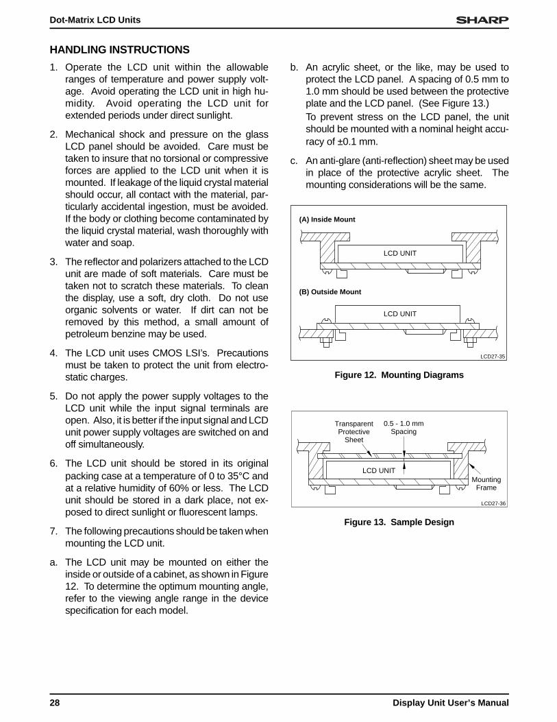
a. The LCD unit may be mounted on either theinside or outside of a cabinet, as shown in Figure12. To determine the optimum mounting angle,refer to the viewing angle range in the devicespecification for each model.
b. An acrylic sheet, or the like, may be used toprotect the LCD panel. A spacing of 0.5 mm to1.0 mm should be used between the protectiveplate and the LCD panel. (See Figure 13.)To prevent stress on the LCD panel, the unitshould be mounted with a nominal height accu-racy of ±0.1 mm.
c. An anti-glare (anti-reflection) sheet may be usedin place of the protective acrylic sheet. Themounting considerations will be the same.
LCD27-35
LCD UNIT
LCD UNIT
(A) Inside Mount
(B) Outside Mount
Figure 12. Mounting Diagrams
LCD27-36
LCD UNIT
TransparentProtective
Sheet
0.5 - 1.0 mmSpacing
MountingFrame
Figure 13. Sample Design
Dot-Matrix LCD Units
28 Display Unit User’s Manual

OPERATING RESTRICTIONS
The LSI (HD44780AXX) used in the LCD units isreported to have the following defects:
HD44780AXX Defective Functions
1. When the display clear or display/cursor homeinstruction is executed when the display hasbeen shifted from its original position, originaldisplay position may not be restored.
2. When the display/cursor home instruction isexecuted, the data in the following display dataRAM locations may be lost.
To counteract these defects. The following re-strictions should be followed (Table 16).
In the production facility, the LSI device in ques-tion is now being replaced with a modified version,HD44780RAXX. The above mentioned restrictionsdo not apply to products using the "RA" version ofthe LSI. The "RA" version devices have an "R"
printed in the upper, right corner, as shown.
LCD27-37
00 01 02 03 04 05 06 07 41 42 43 44 45 46 47 48 49 4A 4B 4C 4D 4E 4F
00 01 02 03 04 05 06 07
. . . . . .
1A 1B 1C 1D 1E 1F 20 21 22 23 24 25 26 27. . .
40 41 42 43 44 45 46 47 5A 5B 5C 5D 5E 5F 60 61 62 63 64 65 66 67. . .
. . .
. . .
Address HEX
Address HEX
Address HEX
A. Address type a.
B. Address type b and c.
Total: 80 Characters
Total: 40 Characters x 2 Lines The contents of address locations23, 27, 63, and 67 may be lostduring the execution of thedisplay/cursor home instruction.NOTE: Although address type C is for a single-line display its
address structure is logically the same as for address type b.
The contents of addresses (43), (47), (4B),and (4F) may be destroyed.
12 23(5$7,21 5(675,&7,21
([HFXWLRQ RI WKH GLVSOD\ FOHDU RU GLVSOD\FXUVRU KRPHLQVWUXFWLRQ ZKHQ WKH GLVSOD\ KDV EHHQ VKLIWHG IURP LWVRULJLQDO SRVLWLRQ
7KH GLVSOD\FXUVRU KRPH LQVWUXFWLRQ VKRXOG EH H[HFXWHG DIWHU WKH GHIHFWLYH LQVWUXFWLRQEXW DIWHU D WLPH LQWHUYDO QRW HTXDO WR DQ\ PXOWLSOH RI I26& N+] VHFRQGV6LQFH I26& N+] WKH IROORZLQJ WLPLQJ LQWHUYDOV VKRXOG EH DYRLGHG VHFRQGV VHFRQGV VHFRQGV HWF
([HFXWLRQ RI WKHGLVSOD\FXUVRUKRPH LQVWUXFWLRQ
,Q WKH FDVH RI DGGUHVV W\SH D ZKHQ ''5$0 DGGUHVV ORFDWLRQV % DQG) DUH LQ XVH
%HIRUH H[HFXWLQJ WKH GLVSOD\FXUVRU KRPH LQVWUXFWLRQ WKH GDWD LQ WKH IRXU DGGUHVVORFDWLRQV LQ TXHVWLRQ VKRXOG EH VDYHG HOVHZKHUH E\ WKH PLFURSURFHVVRU $IWHUH[HFXWLRQ RI WKH GLVSOD\FXUVRU KRPH LQVWUXFWLRQ WKH GDWD PD\ EH UHVWRUHG WR WKH ''5$0,Q WKH FDVH RI DGGUHVV W\SHV E DQG F
ZKHQ '' 5$0 DGGUHVV ORFDWLRQV DQG DUH LQ XVH
Table 16.
R
HD44780A
Dot-Matrix LCD Units
Display Unit User’s Manual 29
SHARP Microelectronics of the Americas
Corporation Regional Sales Offices:
North American Headquarters
Camas, WAPh (360) 834-2500Fax (360) 834-8903
West
Huntington Beach, CAPh (714) 903-4600Fax (714) 903-0295
San Jose, CAPh (408) 436-4900Fax (408) 436-0924
Central
Romeoville, ILPh (630) 226-2400Fax (630) 759-8572
Auburn Hills, MIPh (248) 377-9220Fax (248) 377-9222
Austin, TXPh (512) 349-7262Fax (512) 349-7002
DFW Airport, TXPh (972) 456-8560Fax (972) 456-0360
Houston, TXPh (281) 955-9909Fax (281) 955-9910
East
Burlington, MA Ph (781) 270-7979Fax (781) 229-9117
Annandale, NJPh (908) 713-0505Fax (908) 713-0312
Research Triangle Park, NCPh (919) 941-0065Fax (919) 941-0066
Distributors:
Bell/MilgrayEl Segundo, CA
Ph (310) 563-2355Fax (310) 563-2514
Future ElectronicsCanada
Ph (514) 694-7710Fax (514) 695-3707
Marshall IndustriesEl Monte, CA
Ph (800) 522-0084Fax (818) 307-6173www.marshall.com
ReptronTampa, FL
Ph (800) 659-1361Fax (813) 854-4695
Sterling Electronics Corp.Houston, TX
Ph (800) 745-5500Fax (713) 629-3939
Ref. SMT99007