Embed Size (px)
Citation preview
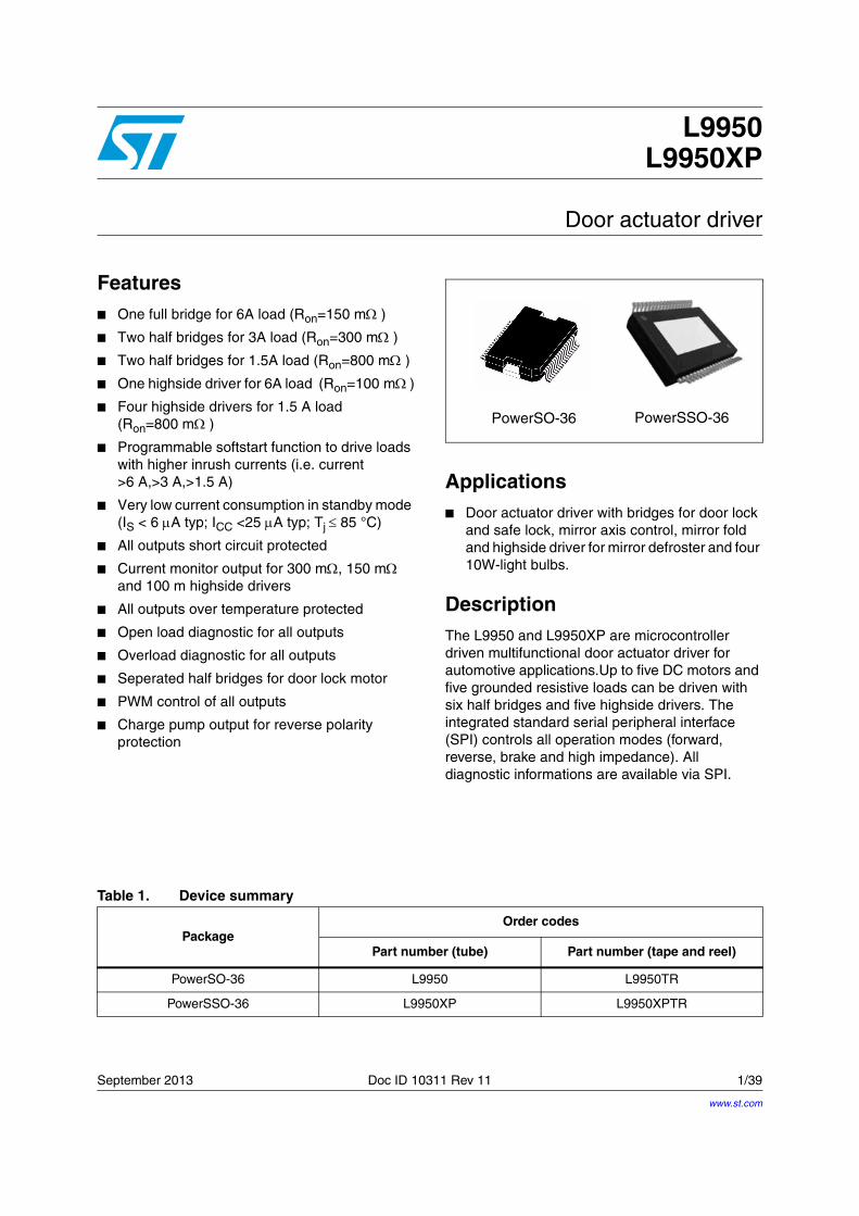
September 2013 Doc ID 10311 Rev 11 1/39
1
L9950L9950XP
Door actuator driver
Features■ One full bridge for 6A load (Ron=150 m )
■ Two half bridges for 3A load (Ron=300 m )
■ Two half bridges for 1.5A load (Ron=800 m )
■ One highside driver for 6A load (Ron=100 m )
■ Four highside drivers for 1.5 A load (Ron=800 m )
■ Programmable softstart function to drive loads with higher inrush currents (i.e. current >6 A,>3 A,>1.5 A)
■ Very low current consumption in standby mode (IS < 6 A typ; ICC <25 A typ; Tj 85 °C)
■ All outputs short circuit protected
■ Current monitor output for 300 m, 150 m and 100 m highside drivers
■ All outputs over temperature protected
■ Open load diagnostic for all outputs
■ Overload diagnostic for all outputs
■ Seperated half bridges for door lock motor
■ PWM control of all outputs
■ Charge pump output for reverse polarity protection
Applications■ Door actuator driver with bridges for door lock
and safe lock, mirror axis control, mirror fold and highside driver for mirror defroster and four 10W-light bulbs.
DescriptionThe L9950 and L9950XP are microcontroller driven multifunctional door actuator driver for automotive applications.Up to five DC motors and five grounded resistive loads can be driven with six half bridges and five highside drivers. The integrated standard serial peripheral interface (SPI) controls all operation modes (forward, reverse, brake and high impedance). All diagnostic informations are available via SPI.
PowerSO-36 PowerSSO-36
Table 1. Device summary
PackageOrder codes
Part number (tube) Part number (tape and reel)
PowerSO-36 L9950 L9950TR
PowerSSO-36 L9950XP L9950XPTR
www.st.com
Contents L9950 - L9950XP
2/39 Doc ID 10311 Rev 11
Contents
1 Block diagram and pin description . . . . . . . . . . . . . . . . . . . . . . . . . . . . . 6
2 Electrical specifications . . . . . . . . . . . . . . . . . . . . . . . . . . . . . . . . . . . . . . 9
2.1 Absolute maximum ratings . . . . . . . . . . . . . . . . . . . . . . . . . . . . . . . . . . . . . 9
2.2 ESD protection . . . . . . . . . . . . . . . . . . . . . . . . . . . . . . . . . . . . . . . . . . . . . . 9
2.3 Thermal data . . . . . . . . . . . . . . . . . . . . . . . . . . . . . . . . . . . . . . . . . . . . . . . 9
2.4 Temperature warning and thermal shutdown . . . . . . . . . . . . . . . . . . . . . . 10
2.5 Electrical characteristics . . . . . . . . . . . . . . . . . . . . . . . . . . . . . . . . . . . . . . 10
2.6 SPI - electrical characteristics . . . . . . . . . . . . . . . . . . . . . . . . . . . . . . . . . 14
3 Application information . . . . . . . . . . . . . . . . . . . . . . . . . . . . . . . . . . . . . 20
3.1 Dual power supply: VS and VCC . . . . . . . . . . . . . . . . . . . . . . . . . . . . . . . 20
3.2 Standby mode . . . . . . . . . . . . . . . . . . . . . . . . . . . . . . . . . . . . . . . . . . . . . 20
3.3 Inductive loads . . . . . . . . . . . . . . . . . . . . . . . . . . . . . . . . . . . . . . . . . . . . . 20
3.4 Diagnostic functions . . . . . . . . . . . . . . . . . . . . . . . . . . . . . . . . . . . . . . . . . 20
3.5 Overvoltage and under voltage detection . . . . . . . . . . . . . . . . . . . . . . . . . 21
3.6 Temperature warning and thermal shutdown . . . . . . . . . . . . . . . . . . . . . . 21
3.7 Open-load detection . . . . . . . . . . . . . . . . . . . . . . . . . . . . . . . . . . . . . . . . . 21
3.8 Over load detection . . . . . . . . . . . . . . . . . . . . . . . . . . . . . . . . . . . . . . . . . 21
3.9 Current monitor . . . . . . . . . . . . . . . . . . . . . . . . . . . . . . . . . . . . . . . . . . . . 22
3.10 PWM inputs . . . . . . . . . . . . . . . . . . . . . . . . . . . . . . . . . . . . . . . . . . . . . . . 22
3.11 Cross current protection . . . . . . . . . . . . . . . . . . . . . . . . . . . . . . . . . . . . . . 22
3.12 Programmable soft start function to drive loads with higher inrush current . 22
4 Functional description of the SPI . . . . . . . . . . . . . . . . . . . . . . . . . . . . . 24
4.1 Serial Peripheral Interface (SPI) . . . . . . . . . . . . . . . . . . . . . . . . . . . . . . . . 24
4.2 Chip Select Not (CSN) . . . . . . . . . . . . . . . . . . . . . . . . . . . . . . . . . . . . . . . 24
4.3 Serial Data In (DI) . . . . . . . . . . . . . . . . . . . . . . . . . . . . . . . . . . . . . . . . . . 24
4.4 Serial Data Out (DO) . . . . . . . . . . . . . . . . . . . . . . . . . . . . . . . . . . . . . . . . 25
4.5 Serial clock (CLK) . . . . . . . . . . . . . . . . . . . . . . . . . . . . . . . . . . . . . . . . . . . 25
4.6 Input data register . . . . . . . . . . . . . . . . . . . . . . . . . . . . . . . . . . . . . . . . . . 25

L9950 - L9950XP Contents
Doc ID 10311 Rev 11 3/39
4.7 Status register . . . . . . . . . . . . . . . . . . . . . . . . . . . . . . . . . . . . . . . . . . . . . 25
4.8 Test mode . . . . . . . . . . . . . . . . . . . . . . . . . . . . . . . . . . . . . . . . . . . . . . . . . 26
5 Packages thermal data . . . . . . . . . . . . . . . . . . . . . . . . . . . . . . . . . . . . . . 31
6 Package and packing information . . . . . . . . . . . . . . . . . . . . . . . . . . . . . 32
6.1 ECOPACK® . . . . . . . . . . . . . . . . . . . . . . . . . . . . . . . . . . . . . . . . . . . . . . . 32
6.2 PowerSO-36 package information . . . . . . . . . . . . . . . . . . . . . . . . . . . . . . 32
6.3 PowerSSO-36 package information . . . . . . . . . . . . . . . . . . . . . . . . . . . . . 34
6.4 PowerSO-36 packing information . . . . . . . . . . . . . . . . . . . . . . . . . . . . . . . 35
6.5 PowerSSO-36 packing information . . . . . . . . . . . . . . . . . . . . . . . . . . . . . 37
7 Revision history . . . . . . . . . . . . . . . . . . . . . . . . . . . . . . . . . . . . . . . . . . . 38

List of tables L9950 - L9950XP
4/39 Doc ID 10311 Rev 11
List of tables
Table 1. Device summary . . . . . . . . . . . . . . . . . . . . . . . . . . . . . . . . . . . . . . . . . . . . . . . . . . . . . . . . . . 1Table 2. Pin definitions and functions . . . . . . . . . . . . . . . . . . . . . . . . . . . . . . . . . . . . . . . . . . . . . . . . . 6Table 3. Absolute maximum ratings . . . . . . . . . . . . . . . . . . . . . . . . . . . . . . . . . . . . . . . . . . . . . . . . . . 9Table 4. ESD protection . . . . . . . . . . . . . . . . . . . . . . . . . . . . . . . . . . . . . . . . . . . . . . . . . . . . . . . . . . . 9Table 5. Thermal data. . . . . . . . . . . . . . . . . . . . . . . . . . . . . . . . . . . . . . . . . . . . . . . . . . . . . . . . . . . . . 9Table 6. Temperature warning and thermal shutdown . . . . . . . . . . . . . . . . . . . . . . . . . . . . . . . . . . . 10Table 7. Supply . . . . . . . . . . . . . . . . . . . . . . . . . . . . . . . . . . . . . . . . . . . . . . . . . . . . . . . . . . . . . . . . . 10Table 8. Overvoltage and under voltage detection . . . . . . . . . . . . . . . . . . . . . . . . . . . . . . . . . . . . . . 11Table 9. Current monitor output . . . . . . . . . . . . . . . . . . . . . . . . . . . . . . . . . . . . . . . . . . . . . . . . . . . . 11Table 10. Charge pump output . . . . . . . . . . . . . . . . . . . . . . . . . . . . . . . . . . . . . . . . . . . . . . . . . . . . . . 11Table 11. OUT1 - OUT11 . . . . . . . . . . . . . . . . . . . . . . . . . . . . . . . . . . . . . . . . . . . . . . . . . . . . . . . . . . 12Table 12. Delay time from standby to active mode. . . . . . . . . . . . . . . . . . . . . . . . . . . . . . . . . . . . . . . 14Table 13. Inputs: CSN, CLK, PWM1/2 and DI . . . . . . . . . . . . . . . . . . . . . . . . . . . . . . . . . . . . . . . . . . 14Table 14. DI timing . . . . . . . . . . . . . . . . . . . . . . . . . . . . . . . . . . . . . . . . . . . . . . . . . . . . . . . . . . . . . . . 15Table 15. DO . . . . . . . . . . . . . . . . . . . . . . . . . . . . . . . . . . . . . . . . . . . . . . . . . . . . . . . . . . . . . . . . . . . 15Table 16. DO timing . . . . . . . . . . . . . . . . . . . . . . . . . . . . . . . . . . . . . . . . . . . . . . . . . . . . . . . . . . . . . . 16Table 17. CSN timing . . . . . . . . . . . . . . . . . . . . . . . . . . . . . . . . . . . . . . . . . . . . . . . . . . . . . . . . . . . . . 16Table 18. Test mode. . . . . . . . . . . . . . . . . . . . . . . . . . . . . . . . . . . . . . . . . . . . . . . . . . . . . . . . . . . . . . 26Table 19. SPI - input data and status registers 0 . . . . . . . . . . . . . . . . . . . . . . . . . . . . . . . . . . . . . . . . 27Table 20. SPI - input data and status registers 1 . . . . . . . . . . . . . . . . . . . . . . . . . . . . . . . . . . . . . . . . 29Table 21. PowerSO-36 mechanical data . . . . . . . . . . . . . . . . . . . . . . . . . . . . . . . . . . . . . . . . . . . . . . 33Table 22. PowerSSO-36 mechanical data . . . . . . . . . . . . . . . . . . . . . . . . . . . . . . . . . . . . . . . . . . . . . 34Table 23. Document revision history . . . . . . . . . . . . . . . . . . . . . . . . . . . . . . . . . . . . . . . . . . . . . . . . . 38
L9950 - L9950XP List of figures
Doc ID 10311 Rev 11 5/39
List of figures
Figure 1. Block diagram . . . . . . . . . . . . . . . . . . . . . . . . . . . . . . . . . . . . . . . . . . . . . . . . . . . . . . . . . . . . 6Figure 2. Configuration diagram (top view) . . . . . . . . . . . . . . . . . . . . . . . . . . . . . . . . . . . . . . . . . . . . . 8Figure 3. SPI - transfer timing diagram . . . . . . . . . . . . . . . . . . . . . . . . . . . . . . . . . . . . . . . . . . . . . . . 16Figure 4. SPI - input timing . . . . . . . . . . . . . . . . . . . . . . . . . . . . . . . . . . . . . . . . . . . . . . . . . . . . . . . . 17Figure 5. SPI - DO valid data delay time and valid time . . . . . . . . . . . . . . . . . . . . . . . . . . . . . . . . . . 17Figure 6. SPI - DO enable and disable time . . . . . . . . . . . . . . . . . . . . . . . . . . . . . . . . . . . . . . . . . . . 18Figure 7. SPI - driver turn-on/off timing, minimum csn hi time . . . . . . . . . . . . . . . . . . . . . . . . . . . . . . 18Figure 8. SPI - timing of status bit 0 (fault condition) . . . . . . . . . . . . . . . . . . . . . . . . . . . . . . . . . . . . . 19Figure 9. Example of programmable soft start function for inductive loads . . . . . . . . . . . . . . . . . . . . 23Figure 10. Packages thermal data . . . . . . . . . . . . . . . . . . . . . . . . . . . . . . . . . . . . . . . . . . . . . . . . . . . . 31Figure 11. PowerSO-36 package dimensions . . . . . . . . . . . . . . . . . . . . . . . . . . . . . . . . . . . . . . . . . . . 32Figure 12. PowerSSO-36 package dimensions . . . . . . . . . . . . . . . . . . . . . . . . . . . . . . . . . . . . . . . . . . 34Figure 13. PowerSO-36 tube shipment (no suffix) . . . . . . . . . . . . . . . . . . . . . . . . . . . . . . . . . . . . . . . . 35Figure 14. PowerSO-36 tape and reel shipment (suffix “TR”) . . . . . . . . . . . . . . . . . . . . . . . . . . . . . . . 36Figure 15. PowerSSO-36 tube shipment (no suffix) . . . . . . . . . . . . . . . . . . . . . . . . . . . . . . . . . . . . . . 37Figure 16. PowerSSO-36 tape and reel shipment (suffix “TR”) . . . . . . . . . . . . . . . . . . . . . . . . . . . . . . 37

Block diagram and pin description L9950 - L9950XP
6/39 Doc ID 10311 Rev 11
1 Block diagram and pin description
Figure 1. Block diagram
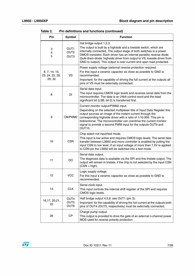
Table 2. Pin definitions and functions
Pin Symbol Function
1, 18, 19, 36 GND
Ground.Reference potential.
Important: for the capability of driving the full current at the outputs all pins of GND must be externally connected.
2, 35 OUT11
Highside driver output 11.The output is built by a highside switch and is intended for resistive loads, hence the internal reverse diode from GND to the output is missing. For ESD reason a diode to GND is present but the energy which can be dissipated is limited. The highside driver is a power DMOS transistor with an internal parasitic reverse diode from the output to VS (bulk-drain-diode). The output is over-current and open load protected.
Important: for the capability of driving the full current at the outputs both pins of OUT11 must be externally connected.
OUT1
Dri
ver
Inte
rfac
e &
Dia
gn
ost
ic
OUT2
OUT3M
SP
IIn
terf
ace
ChargePump
CM / PWM2
CSN
CLK
DO
DI
VS
VCCVCC
VBAT
µC
GND
Lock
1k
MUX5
PWM1
OUT7
OUT8
1k
1k
1k
1k
1k
100k
10k
* Note: Value of capacitor has to be choosen carefully to limit the VSvoltage below absolute maximum ratings in case of an unexpected
freewheeling condition of inductive loads (e.g. TSD, POR)
*
** Note: Resistors between µC and L9950 are recommended to limit currentsfor negative voltage transients at VBAT (e.g. ISO type 1 pulse)
+ Note: Using a ferrite instead of 10ohm will additionally improve EMC behavior
ReversePolarity
Protection
**
**
********
100µF
Safe Lock
M
100nF
VREG
100 10
100nF
CP
EMCOptimization
+
Exterior Light
Safety LightOUT9
OUT10
OUT11
OUT4
OUT5
OUT6
M
M
MFolder
xy-MirrorMotors
Footstep Light
Turn Indicator
Defroster
L9950 - L9950XP Block diagram and pin description
Doc ID 10311 Rev 11 7/39
345
OUT1 OUT2OUT3
Hal bridge output 1,2,3.
The output is built by a highside and a lowside switch, which are internally connected. The output stage of both switches is a power DMOS transistor. Each driver has an internal parasitic reverse diode (bulk-drain-diode: highside driver from output to VS, lowside driver from GND to output). This output is over-current and open load protected.
6, 7, 14, 15, 23, 24, 25, 28,
29, 32VS
Power supply voltage (external reverse protection required.For this input a ceramic capacitor as close as possible to GND is recommended.Important: for the capability of driving the full current at the outputs all pins of VS must be externally connected.
8 DI
Serial data input.
The input requires CMOS logic levels and receives serial data from the microcontroller. The data is an 24bit control word and the least significant bit (LSB, bit 0) is transferred first.
9 CM/PWM2
Current monitor output/PWM2 input.
Depending on the selected multiplexer bits of Input Data Register this output sources an image of the instant current through the corresponding highside driver with a ratio of 1/10.000. This pin is bidirectional. The microcontroller can overdrive the current monitor signal to provide a second PWM input for the outputs OUT9 and OUT10.
10 CSN
Chip select not input/test mode.This input is low active and requires CMOS logic levels. The serial data transfer between L9950 and micro controller is enabled by pulling the input CSN to low level. If an input voltage of more than 7.5V is applied to CSN pin the L9950 will be switched into a test mode.
11 DO
Serial data output.The diagnosis data is available via the SPI and this tristate output. The output will remain in tristate, if the chip is not selected by the input CSN (CSN = high).
12 VCCLogic supply voltage.
For this input a ceramic capacitor as close as possible to GND is recommended.
13 CLKSerial clock input.This input controls the internal shift register of the SPI and requires CMOS logic levels.
16,17, 20,21,22
OUT4 OUT5 OUT6
Half bridge output 4,5,6: see OUT1 (pin 3).
Important: for the capability of driving the full current at the outputs both pins of OUT4 (OUT5, respectively) must be externally connected.
26 CPCharge pump output.
This output is provided to drive the gate of an external n-channel power MOS used for reverse polarity protection
Table 2. Pin definitions and functions (continued)
Pin Symbol Function

Block diagram and pin description L9950 - L9950XP
8/39 Doc ID 10311 Rev 11
Figure 2. Configuration diagram (top view)
27 PWM1PWM1 input.
This input signal can be used to control the drivers OUT1-OUT8 and OUT11 by an external PWM signal.
30
3133
34
OUT7, OUT8, OUT9, OUT10
Highside driver output 7,8,9,10.The output is built by a highside switch and is intended for resistive loads, hence the internal reverse diode from GND to the output is missing. For ESD reason a diode to GND is present but the energy which can be dissipated is limited. The highside driver is a power DMOS transistor with an internal parasitic reverse diode from the output to VS (bulk-drain-diode). The output is over-current and open load protected.
Table 2. Pin definitions and functions (continued)
Pin Symbol Function
GND 1
OUT11 2
OUT1 3
OUT2 4
OUT3 5
VS 6
VS 7
8
CM/PWM2 9
CSN 10
DO 11
VCC 12
CLK 13
VS 14
VS 15
OUT4 16
OUT4 17
GND 18
DI
GND36
OUT1135
OUT1034
OUT933
VS32
VS
31 OUT8
30
29
VS28
PWM127
CP26
VS25
VS24
VS23
OUT622
OUT521
OUT520
GND19
OUT7
Power SO36
Chip
Leadframe

L9950 - L9950XP Electrical specifications
Doc ID 10311 Rev 11 9/39
2 Electrical specifications
2.1 Absolute maximum ratingsStressing the device above the rating listed in the “Absolute maximum ratings” table may cause permanent damage to the device. These are stress ratings only and operation of the device at these or any other conditions above those indicated in the Operating sections of this specification is not implied. Exposure to Absolute Maximum Rating conditions for extended periods may affect device reliability. Refer also to the STMicroelectronics SURE Program and other relevant quality document.
2.2 ESD protection
2.3 Thermal data
Table 3. Absolute maximum ratings
Symbol Parameter Value Unit
VS
DC supply voltage -0.3 to 28 V
Single pulse tmax < 400 ms 40 V
VCC Stabilized supply voltage, logic supply -0.3 to 5.5 V
VDI, VDO, VCLK, VCSN, Vpwm1
Digital input/output voltage -0.3 to VCC + 0.3 V
VCM Current monitor output -0.3 to VCC + 0.3 V
VCP Charge pump output -25 to VS + 11 V
IOUT1,2,3,6,7,8,9,10 Output current ±5 A
IOUT4,5,11 Output current ±10 A
Table 4. ESD protection
Parameter Value Unit
All pins 4 (1)
1. HBM according to CDF-AEC-Q100-002.
kV
Output pins: OUT1 - OUT11 8 (2)
2. HBM with all unzapped pins grounded.
kV
Table 5. Thermal data
Symbol Parameter Value Unit
Tj Operating junction temperature -40 to 150 °C

Electrical specifications L9950 - L9950XP
10/39 Doc ID 10311 Rev 11
2.4 Temperature warning and thermal shutdown
2.5 Electrical characteristicsVS = 8 to 16 V, VCC = 4.5 to 5.3 V, Tj = - 40 to 150 °C, unless otherwise specified.
The voltages are referred to GND and currents are assumed positive, when the current flows into the pin.
Table 6. Temperature warning and thermal shutdown
Symbol Parameter Min. Typ. Max. Unit
TjTW ONTemperature warning threshold junction temperature
Tj increasing
- - 150 °C
TjTW OFFTemperature warning threshold junction temperature
Tj decreasing
130 - - °C
TjTW HYS Temperature warning hysteresis - 5 - °K
TjSD ONThermal shutdown threshold junction temperature
Tj increasing
- - 170 °C
TjSD OFFThermal shutdown threshold junction temperature
Tj decreasing
150 - - °C
TjSD HYS Thermal shutdown hysteresis - 5 - °K
Table 7. Supply
Symbol Parameter Test condition Min. Typ. Max. Unit
VSOperating supply voltage range
7 - 28 V
IS
VS DC supply current
VS = 16 V, VCC = 5.3 V
active mode
OUT1 - OUT11 floating
- 7 20 mA
VS quiescent supply current
VS = 16 V, VCC = 0 V
standby modeOUT1 - OUT11 floating
Ttest =-40 °C, 25 °C
- 4 12 µA
ICC
VCC DC supply currentVS = 16 V, VCC = 5.3 V
CSN = VCC , active mode- 1 3 mA
VCC quiescent supply current
VS = 16 V, VCC = 5.3 V
CSN = VCCstandby mode
OUT1 - OUT11 floatingTtest =-40 °C, 25 °C
- 25 50 µA
IS + ICCSum quiescent supply current
VS = 16 V, VCC = 5.3 VCSN = VCC
standby mode
OUT1 - OUT11 floatingTtest =-40 °C, 25 °C
- 31 75 µA
L9950 - L9950XP Electrical specifications
Doc ID 10311 Rev 11 11/39
Table 8. Overvoltage and under voltage detection
Symbol Parameter Test condition Min. Typ. Max. Unit
VSUV ON VS UV-threshold voltage VS increasing 5.9 - 7.2 V
VSUV OFF VS UV-threshold voltage VS decreasing 5.5 - 6.5 V
VSUV hyst VS UV-hysteresis VSUV ON - VSUV OFF - 0.5 - V
VSOV OFF VS OV-threshold voltage VS increasing 18 - 24.5 V
VSOV ON VS OV-threshold voltage VS decreasing 17.5 - 22 V
VSOV hyst VS OV-hysteresis VSOV OFF - VSOV ON - 1 - V
VPOR OFF Power-on-reset threshold VCC increasing - - 4.4 V
VPOR ON Power-on-reset threshold VCC decreasing 3.1 - - V
VPOR hyst Power-on-reset hysteresis VPOR OFF - VPOR ON - 0.3 - V
Table 9. Current monitor output
Symbol Parameter Test condition Min. Typ. Max. Unit
VCM Functional voltage range VCC = 5 V 0 4 V
ICM,r
Current monitor output ratio:
ICM / IOUT1,4,5,6,11
0 V VCM 4 V, VCC=5 V - - -
ICM acc Current monitor accuracy
0 V VCM 3.8 V,
VCC = 5 V, IOut,min=500 mA,
IOut4,5,11,max = 5.9 A IOut1,6,max = 2.9 A
(FS = full scale= 600 µA)
-4% +1%FS
8% +2%FS
-
Table 10. Charge pump output
Symbol Parameter Test condition Min. Typ. Max. Unit
VCPCharge pump output voltage
VS = 8 V, ICP = -60 µA 6 - 13 V
VS = 10 V, ICP = -80 µA 8 - 13 V
VS 12 V, ICP = -100 µA 10 - 13 V
ICPCharge pump output current
VCP = VS+10 V, VS =13.5 V 95 150 300 µA
110.000------------------
Electrical specifications L9950 - L9950XP
12/39 Doc ID 10311 Rev 11
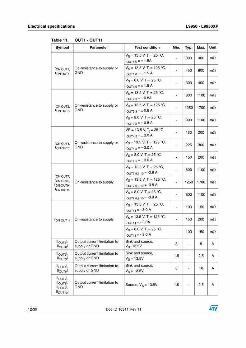
Table 11. OUT1 - OUT11
Symbol Parameter Test condition Min. Typ. Max. Unit
rON OUT1, rON OUT6
On-resistance to supply or GND
VS = 13.5 V, Tj = 25 °C, IOUT1,6 = 1.5A
- 300 400 m
VS = 13.5 V, Tj = 125 °C, IOUT1,6 = 1.5 A
- 450 600 m
VS = 8.0 V, Tj = 25 °C, IOUT1,6 = 1.5 A
- 300 400 m
rON OUT2, rON OUT3
On-resistance to supply or GND
VS = 13.5 V, Tj = 25 °C, IOUT2,3 = 0.8A
- 800 1100 m
VS = 13.5 V, Tj = 125 °C, IOUT2,3 = 0.8 A
- 1250 1700 m
VS = 8.0 V, Tj = 25 °C, IOUT2,3 = 0.8 A
- 800 1100 m
rON OUT4, rON OUT5
On-resistance to supply or GND
VS = 13.5 V, Tj = 25 °C,
IOUT4,5 = 3.0 A- 150 200 m
VS = 13.5 V, Tj = 125 °C,
IOUT4,5 = 3.0 A- 225 300 m
VS = 8.0 V, Tj = 25 °C,
IOUT4,5 = 3.0 A- 150 200 m
rON OUT7, rON OUT8, rON OUT9 , rON OUT10
On-resistance to supply
VS = 13.5 V, Tj = 25 °C,
IOUT7,8,9,10 = -0.8 A- 800 1100 m
VS = 13.5 V, Tj = 125 °C,
IOUT7,8,9,10 = -0.8 A- 1250 1700 m
VS = 8.0 V, Tj = 25 °C,
IOUT7,8,9,10 = -0.8 A- 800 1100 m
rON OUT11 On-resistance to supply
VS = 13.5 V, Tj = 25 °C,
IOUT11 = - 3.0 A- 100 150 m
VS = 13.5 V, Tj = 125 °C,
IOUT11 = - 3.0A- 150 200 m
VS = 8.0 V, Tj = 25 °C,
IOUT11 = - 3.0 A- 100 150 m
|IOUT1|, |IOUT6|
Output current limitation to supply or GND
Sink and source, VS=13.5V
3 - 5 A
|IOUT2|, |IOUT3|
Output current limitation to supply or GND
Sink and source, VS = 13.5V
1.5 - 2.5 A
|IOUT4|, |IOUT5|
Output current limitation to supply or GND
Sink and source, VS = 13.5V
6 - 10 A
|IOUT7|, |IOUT8|, |IOUT9|, |IOUT10|
Output current limitation to GND
Source, VS = 13.5V 1.5 - 2.5 A

L9950 - L9950XP Electrical specifications
Doc ID 10311 Rev 11 13/39
|IOUT11|Output current limitation to GND
Source, VS = 13.5V 6 - 10 A
td ON HOutput delay time,
highside driver on
VS = 13.5 V, corresponding lowside driver is not active
20 40 80 µs
td OFF HOutput delay time,
highside driver offVS = 13.5 V 50 150 300 µs
td ON LOutput delay time,
lowside driver on
VS = 13.5 V, corresponding highside driver is not active
15 30 70 µs
td OFF LOutput delay time,
lowside driver offVS = 13.5 V 80 150 300 µs
tD HLCross current protection time, source to sink
td ON L - td OFF H, - 200 400 µs
tD LHCross current protection time, sink to source
td ON H - td OFF L - 200 400 µs
IQLHSwitched-off output current highside drivers of OUT1-11
VOUT1-11=0 V, standby mode
0 -2 -5 µA
VOUT1-11=0 V, active mode
-40 -15 0 µA
IQLLSwitched-off output current lowside drivers of OUT1-6
VOUT1-6 = VS, standby mode
0 110 180 µA
VOUT1-6 = VS, active mode -40 -15 0 µA
IOLD1Open load detection current of OUT1
5 30 80 mA
IOLD23Open load detection current of OUT2, OUT3
15 40 60 mA
IOLD45Open load detection current of OUT4 and OUT5
60 150 300 mA
IOLD6Open load detection current of OUT6
30 70 150 mA
IOLD78910
Open load detection current of OUT7, OUT8, OUT9, OUT10
15 40 60 mA
IOLD11Open load detection current of OUT11
30 150 300 mA
tdOL
Minimum duration of open load condition to set the status bit
500 - 3000 µs
tISC
Minimum duration of over-current condition to switch off the driver
10 - 100 µs
Table 11. OUT1 - OUT11 (continued)
Symbol Parameter Test condition Min. Typ. Max. Unit

Electrical specifications L9950 - L9950XP
14/39 Doc ID 10311 Rev 11
2.6 SPI - electrical characteristicsVS = 8 to 16 V, VCC = 4.5 to 5.3 V, Tj = - 40 to 150 °C, unless otherwise specified. The voltages are referred to GND and currents are assumed positive, when the current flows into the pin.
Note: Value of input capacity is not measured in production test. Parameter guaranteed by design.
dVOUT16/dt Slew rate of OUT1,OUT6VS =13.5 V
Iload = ±1.5 A0.1 0.2 0.4 V/µs
dVOUT23/dt, dVOUT78910/dt
Slew rate of OUT2/3 and OUT7-OUT10
VS = 13.5 V
Iload = -0.8 A0.09 0.2 0.4 V/µs
dVOUT45/dt Slew rate of OUT4, OUT5VS = 13.5 V
Iload = ±3.0 A0.1 0.2 0.4 V/µs
dVOUT11/dt Slew rate of OUT11VS = 13.5 V
Iload = 3.0 A0.1 0.2 0.4 V/µs
Table 11. OUT1 - OUT11 (continued)
Symbol Parameter Test condition Min. Typ. Max. Unit
Table 12. Delay time from standby to active mode
Symbol Parameter Test condition Min. Typ. Max. Unit
tset Delay timeSwitching from standby to active mode. Time until output drivers are enabled after CSN going to high.
- 160 300 µs
Table 13. Inputs: CSN, CLK, PWM1/2 and DI
Symbol Parameter Test condition Min. Typ. Max. Unit
VinL Input low level VCC = 5 V 1.5 2.0 - V
VinH Input high level VCC = 5 V - 3.0 3.5 V
VinHyst Input hysteresis VCC = 5 V 0.5 - - V
ICSN in Pull up current at input CSN VCSN = 3.5 V VCC = 5 V -40 -20 -8 µA
ICLK in Pull down current at input CLK VCLK = 1.5 V 10 25 50 µA
IDI in Pull down current at input DI VDI = 1.5 V 10 25 50 µA
IPWM1 inPull down current at input PWM1
VPWM = 1.5 V 10 25 50 µA
Cin Input capacitance at input CSN, CLK, DI and PWM1/2
VCC = 0 to 5.3 V - 10 15 pF

L9950 - L9950XP Electrical specifications
Doc ID 10311 Rev 11 15/39
Note: DI timing parameters tested in production by a passed/failed test:Tj=-40 °C/+25 °C: SPI communication @2 MHZ.Tj=+125 °C: SPI communication @1.25 MHZ.
Table 14. DI timing
Symbol Parameter Test condition Min. Typ. Max. Unit
tCLK Clock period VCC = 5 V 1000 - - ns
tCLKH Clock high time VCC = 5 V 400 - - ns
tCLKL Clock low time VCC = 5 V 400 - - ns
tset CSNCSN setup time, CSN low before rising edge of CLK
VCC = 5 V 400 - - ns
tset CLKCLK setup time, CLK high before rising edge of CSN
VCC = 5 V 400 - - ns
tset DI DI setup time VCC = 5 V 200 - - ns
thold time DI hold time VCC = 5 V 200 - - ns
tr inRise time of input signal DI, CLK, CSN
VCC = 5 V - - 100 ns
tf inFall time of input signal DI, CLK, CSN
VCC = 5 V - - 100 ns
Table 15. DO
Symbol Parameter Test condition Min. Typ. Max. Unit
VDOL Output low level VCC = 5 V, ID = -2 mA - 0.2 0.4 V
VDOH Output high level VCC = 5 V, ID = 2 mA VCC -0.4 VCC-0.2 - V
IDOLK Tristate leakage currentVCSN = VCC, 0 V < VDO < VCC
-10 - 10 µA
CDO(1)
1. Value of input capacity is not measured in production test. Parameter guaranteed by design.
Tristate input capacitance
VCSN = VCC,0 V < VCC < 5.3 V
- 10 15 pF

Electrical specifications L9950 - L9950XP
16/39 Doc ID 10311 Rev 11
Figure 3. SPI - transfer timing diagram
Table 16. DO timing
Symbol Parameter Test condition Min. Typ. Max. Unit
tr DO DO rise time CL = 100 pF, Iload = -1 mA - 80 140 ns
tf DO DO fall time CL = 100 pF, Iload = 1 mA - 50 100 ns
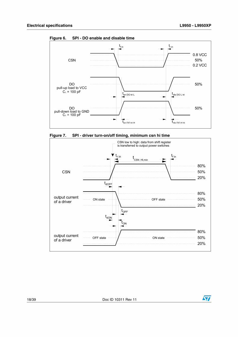
ten DO tri LDO enable time
from tristate to low level
CL = 100 pF, Iload = 1 mA
pull-up load to VCC- 100 250 ns
tdis DO L triDO disable time
from low level to tristate
CL = 100 pF, Iload = 4 mA
pull-up load to VCC- 380 450 ns
ten DO tri HDO enable time
from tristate to high level
CL =100 pF, Iload = -1 mA
pull-down load to GND- 100 250 ns
tdis DO H triDO disable time
from high level to tristate
CL = 100 pF, Iload = -4 mA
pull-down load to GND- 380 450 ns
td DO DO delay timeVDO < 0.3 VCC, VDO > 0.7 VCC,
CL = 100 pF - 50 250 ns
Table 17. CSN timing
Symbol Parameter Test condition Min. Typ. Max. Unit
tCSN_HI,stbMinimum CSN HI time, switching from standby mode
Transfer of SPI command to Input Register
- 20 50 µs
tCSN_HI,minMaximum CSN HI time, active mode
Transfer of SPI command to input register
- 2 4 µs
1 2 3 4 5 6 70 0 1
1 2 3 4 5 6 70
1 2 3 4 5 6 70
0 1
0 1
CSN
CLK
DI
DO
Input Data
Register
CSN high to low: DO enabled
time
DI: data will be accepted on the rising edge of CLK signal time
time
time
time
DO: data will change on the falling edge of CLK signal
fault bit CSN low to high: actual data is transfered to output power switches
old data new data
232221201918
232221201918
232221201918
XX
XX
XX
1 2 3 4 5 6 70 0 1
1 2 3 4 5 6 70
1 2 3 4 5 6 70 0 1
1 2 3 4 5 6 70
1 2 3 4 5 6 70
0 1
0 1
CSN
CLK
DI
DO
Input Data
Register
CSN high to low: DO enabled
time
DI: data will be accepted on the rising edge of CLK signal time
time
time
time
DO: data will change on the falling edge of CLK signal
fault bit CSN low to high: actual data is transfered to output power switches
old data new data
232221201918
232221201918
232221201918
XX
XX
XX

L9950 - L9950XP Electrical specifications
Doc ID 10311 Rev 11 17/39
Figure 4. SPI - input timing
Figure 5. SPI - DO valid data delay time and valid time
0.8 VCC
0.8 VCC
0.8 VCC
0.2 VCC
0.2 VCC
0.2 VCCValid Valid
CSN
CLK
DI
tset CSN
tCLKH
tset CLK
tCLKL
thold DI
tset DI
0.8 VCC
0.8 VCC
0.8 VCC
0.2 VCC
0.2 VCC
0.2 VCC
CLK
DO(low to high)
DO(high to low)
0.5 VCC
tr in
tr DO
tf DO
td DO
tf in
Electrical specifications L9950 - L9950XP
18/39 Doc ID 10311 Rev 11
Figure 6. SPI - DO enable and disable time
Figure 7. SPI - driver turn-on/off timing, minimum csn hi time
CSN
tf in r int
DO
DO
en DO tri Lt tdis DO L tri
50%
0.8 VCC
0.2 VCC
50%
50%
en DO tri Ht tdis DO H tri
C = 100 pFL
C = 100 pFL
pull-up load to VCC
pull-down load to GND
CSN
dONt
20%
80%
tr in f int
OFFt
dOFFt
OFF state
ON state OFF state
ON state
ONt
output currentof a driver
50%
50%
80%
20%
20%
80%
50%output currentof a driver
CSN low to high: data from shift register is transferred to output power switches
tCSN_HI,min
L9950 - L9950XP Electrical specifications
Doc ID 10311 Rev 11 19/39
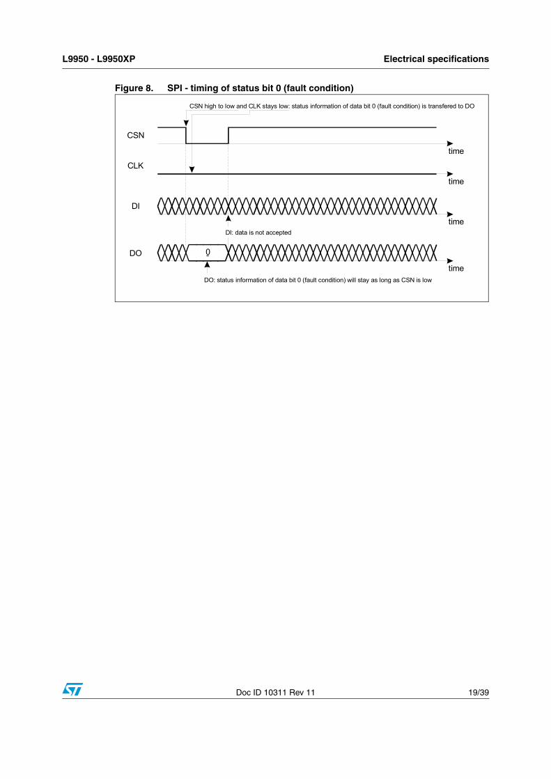
Figure 8. SPI - timing of status bit 0 (fault condition)
CSN
CLK
DI
DO
CSN high to low and CLK stays low: status information of data bit 0 (fault condition) is transfered to DO
DI: data is not accepted
DO: status information of data bit 0 (fault condition) will stay as long as CSN is low
time
time
time
time
0-

Application information L9950 - L9950XP
20/39 Doc ID 10311 Rev 11
3 Application information
3.1 Dual power supply: VS and VCC
The power supply voltage VS supplies the half bridges and the highside drivers. An internal charge-pump is used to drive the highside switches. The logic supply voltage VCC (stabilized 5 V) is used for the logic part and the SPI of the device.
Due to the independent logic supply voltage the control and status information will not be lost, if there are temporary spikes or glitches on the power supply voltage. In case of power-on (VCC increases from under voltage to VPOR OFF = 4.2 V) the circuit is initialized by an internally generated power on reset (POR). If the voltage VCC decreases under the minimum threshold (VPOR ON = 3.4 V), the outputs are switched to tristate (high impedance) and the status registers are cleared.
3.2 Standby modeThe standby mode of the L9950 is activated by clearing the bit 23 of the Input Data Register 0. All latched data will be cleared and the inputs and outputs are switched to high impedance. In the standby mode the current at VS (VCC) is less than 6 µA (50 µA) for CSN = high (DO in tristate). By switching the VCC voltage a very low quiescent current can be achieved. If bit 23 is set, the device will be switched to active mode.
3.3 Inductive loadsEach half bridge is built by an internally connected highside and a lowside power DMOS transistor. Due to the built-in reverse diodes of the output transistors, inductive loads can be driven at the outputs OUT1 to OUT6 without external free wheeling diodes. The highside drivers OUT7 to OUT11 are intended to drive resistive loads. Hence only a limited energy (E<1 mJ) can be dissipated by the internal ESD diodes in freewheeling condition. For inductive loads (L>100 µH) an external free wheeling diode connected to GND and the corresponding output is needed.
3.4 Diagnostic functionsAll diagnostic functions (over/open load, power supply over-/undervoltage, temperature warning and thermal shutdown) are internally filtered and the condition has to be valid for at least 32 µs (open load: 1 ms, respectively) before the corresponding status bit in the status registers will be set. The filters are used to improve the noise immunity of the device. Open load and temperature warning function are intended for information purpose and will not change the state of the output drivers. On contrary, the overload and thermal shutdown condition will disable the corresponding driver (overload) or all drivers (thermal shutdown), respectively. Without setting the over-current recovery bits in the Input Data register, the microcontroller has to clear the over-current status bits to reactivate the corresponding drivers.

L9950 - L9950XP Application information
Doc ID 10311 Rev 11 21/39
3.5 Overvoltage and under voltage detectionIf the power supply voltage VS rises above the overvoltage threshold VSOV OFF (typical 21 V), the outputs OUT1 to OUT11 are switched to high impedance state to protect the load. When the voltage VS drops below the under voltage threshold VSUV OFF (UV switch OFF voltage), the output stages are switched to the high impedance to avoid the operation of the power devices without sufficient gate driving voltage (increased power dissipation). If the supply voltage VS recovers to normal operating voltage the outputs stages return to the programmed state (input register 0: bit 20=0).
If the under voltage/overvoltage recovery disable bit is set, the automatic turn-on of the drivers is deactivated. The microcontroller needs to clear the status bits to reactivate the drivers. It is recommended to set bit 20 to avoid a possible high current oscillation in case of a shorted output to GND and low battery voltage.
3.6 Temperature warning and thermal shutdownIf junction temperature rises above Tj TW a temperature warning flag is set and is detectable via the SPI. If junction temperature increases above the second threshold Tj SD, the thermal shutdown bit will be set and power DMOS transistors of all output stages are switched off to protect the device. In order to reactivate the output stages the junction temperature must decrease below Tj SD - Tj SD HYS and the thermal shutdown bit has to be cleared by the microcontroller.
3.7 Open-load detectionThe open load detection monitors the load current in each activated output stage. If the load current is below the open load detection threshold for at least 1 ms (tdOL) the corresponding open load bit is set in the status register. Due to mechanical/electrical inertia of typical loads a short activation of the outputs (e.g. 3ms) can be used to test the open load status without changing the mechanical/electrical state of the loads.
3.8 Over load detectionIn case of an over-current condition a flag is set in the status register in the same way as open load detection. If the over-current signal is valid for at least tISC = 32 µs, the over-current flag is set and the corresponding driver is switched off to reduce the power dissipation and to protect the integrated circuit. If the over-current recovery bit of the output is zero the microcontroller has to clear the status bits to reactivate the corresponding driver.

Application information L9950 - L9950XP
22/39 Doc ID 10311 Rev 11
3.9 Current monitorThe current monitor output sources a current image at the current monitor output which has a fixed ratio (1/10000) of the instantaneous current of the selected highside driver. The bits 18 and 19 of the Input Data Register 0 control which of the outputs OUT1, OUT4, OUT5, OUT6 and OUT11 will be multiplexed to the current monitor output. The current monitor output allows a more precise analysis of the actual state of the load rather than the detection of an open or overload condition. For example this can be used to detect the motor state (starting, free running, stalled). Moreover, it is possible to regulate the power of the defroster more precise by measuring the load current. The current monitor output is bidirectional (c.f. PWM inputs).
3.10 PWM inputsEach driver has a corresponding PWM enable bit which can be programmed by the SPI interface. If the PWM enable bit is set, the output is controlled by the logically AND combination of the PWM signal and the output control bit in Input Data Register. The outputs OUT1-OUT8 and OUT11 are controlled by the PWM1 input and the outputs OUT9/10 are controlled by the bidirectional input CM/PMW2. For example, the two PWM inputs can be used to dim two lamps independently by external PWM signals.
3.11 Cross current protectionThe six half brides of the device are cross current protected by an internal delay time. If one driver (LS or HS) is turned off the activation of the other driver of the same half bridge will be automatically delayed by the cross current protection time. After the cross current protection time is expired the slew rate limited switch off phase of the driver will be changed to a fast turn-off phase and the opposite driver is turned on with slew rate limitation. Due to this behavior it is always guaranteed that the previously activated driver is totally turned off before the opposite driver will start to conduct.
3.12 Programmable soft start function to drive loads with higher inrush currentLoads with start-up currents higher than the over-current limits (e.g. inrush current of lamps, start current of motors and cold resistance of heaters) can be driven by using the programmable soft start function (i.e. overcurrent recovery mode). Each driver has a corresponding over-current recovery bit. If this bit is set, the device will automatically switch-on the outputs again after a programmable recovery time. The duty cycle in over-current condition can be programmed by the SPI interface to be about 12% or 25%. The PWM modulated current will provide sufficient average current to power up the load (e.g. heat up the bulb) until the load reaches operating condition.
The device itself cannot distinguish between a real overload and a non linear load like a light bulb. A real overload condition can only be qualified by time. As an example the microcontroller can switch on light bulbs by setting the over-current Recovery bit for the first 50ms. After clearing the recovery bit the output will be automatically disabled if the overload condition still exits.

L9950 - L9950XP Application information
Doc ID 10311 Rev 11 23/39
Figure 9. Example of programmable soft start function for inductive loads

Functional description of the SPI L9950 - L9950XP
24/39 Doc ID 10311 Rev 11
4 Functional description of the SPI
4.1 Serial Peripheral Interface (SPI)This device uses a standard SPI to communicate with a microcontroller. The SPI can be driven by a microcontroller with its SPI peripheral running in following mode: CPOL = 0 and CPHA = 0.
For this mode, input data is sampled by the low to high transition of the clock CLK, and output data is changed from the high to low transition of CLK.
This device is not limited to microcontroller with a build-in SPI. Only three CMOS-compatible output pins and one input pin will be needed to communicate with the device. A fault condition can be detected by setting CSN to low. If CSN = 0, the DO pin will reflect the status bit 0 (fault condition) of the device which is a logical or of all bits in the status registers 0 and 1. The microcontroller can poll the status of the device without the need of a full SPI communication cycle.
Note: In contrast to the SPI standard the least significant bit (LSB) will be transferred first(see Figure 3).
4.2 Chip Select Not (CSN)The input pin is used to select the serial interface of this device. When CSN is high, the output pin (DO) will be in high impedance state. A low signal will activate the output driver and a serial communication can be started. The state when CSN is going low until the rising edge of CSN will be called a communication frame. If the CSN input pin is driven above 7.5V, the L9950 will go into a test mode. In the test mode the DO will go from tri state to active mode.
4.3 Serial Data In (DI)The input pin is used to transfer data serial into the device. The data applied to the DI will be sampled at the rising edge of the CLK signal and shifted into an internal 24 bit shift register. At the rising edge of the CSN signal the contents of the shift register will be transferred to Data Input Register. The writing to the selected Data Input Register is only enabled if exactly 24 bits are transmitted within one communication frame (i.e. CSN low). If more or less clock pulses are counted within one frame the complete frame will be ignored. This safety function is implemented to avoid an activation of the output stages by a wrong communication frame.
Note: Due to this safety functionality a daisy chaining of SPI is not possible. Instead, a parallel operation of the SPI bus by controlling the CSN signal of the connected ICs is recommended.
L9950 - L9950XP Functional description of the SPI
Doc ID 10311 Rev 11 25/39
4.4 Serial Data Out (DO)The data output driver is activated by a logical low level at the CSN input and will go from high impedance to a low or high level depending on the status bit 0 (fault condition). The first rising edge of the CLK input after a high to low transition of the CSN pin will transfer the content of the selected status register into the data out shift register. Each subsequent falling edge of the CLK will shift the next bit out.
4.5 Serial clock (CLK)The CLK input is used to synchronize the input and output serial bit streams. The data input (DI) is sampled at the rising edge of the CLK and the data output (DO) will change with the falling edge of the CLK signal.
4.6 Input data registerThe device has two input registers. The first bit (bit 0) at the DI input is used to select one of the two Input Registers. All bits are first shifted into an input shift register. After the rising edge of CSN the contents of the input shift register will be written to the selected Input Data Register only if a frame of exact 24 data bits are detected. Depending on bit 0 the contents of the selected status register will be transferred to DO during the current communication frame. Bit 1-17 controls the behavior of the corresponding driver.
If bit 23 is zero, the device will go into the standby mode. The bits 18 and 19 are used to control the current monitor multiplexer. Bit 22 is used to reset all status bits in both status registers. The bits in the status registers will be cleared after the current communication frame (rising edge of CSN).
4.7 Status registerThis devices uses two status registers to store and to monitor the state of the device. Bit 0 is used as a fault bit and is a logical NOR combination of bits 1-22 in both status registers. The state of this bit can be polled by the microcontroller without the need of a full SPI communication cycle. If one of the over-current bits is set, the corresponding driver will be disabled. If the over-current recovery bit of the output is not set the microcontroller has to clear the over-current bit to enable the driver. If the thermal shutdown bit is set, all drivers will go into a high impedance state. Again the microcontroller has to clear the bit to enable the drivers.
Functional description of the SPI L9950 - L9950XP
26/39 Doc ID 10311 Rev 11
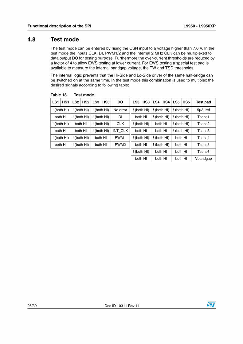
4.8 Test modeThe test mode can be entered by rising the CSN input to a voltage higher than 7.0 V. In the test mode the inputs CLK, DI, PWM1/2 and the internal 2 MHz CLK can be multiplexed to data output DO for testing purpose. Furthermore the over-current thresholds are reduced by a factor of 4 to allow EWS testing at lower current. For EWS testing a special test pad is available to measure the internal bandgap voltage, the TW and TSD thresholds.
The internal logic prevents that the Hi-Side and Lo-Side driver of the same half-bridge can be switched on at the same time. In the test mode this combination is used to multiplex the desired signals according to following table:
Table 18. Test mode
LS1 HS1 LS2 HS2 LS3 HS3 DO LS3 HS3 LS4 HS4 LS5 HS5 Test pad
! (both HI) ! (both HI) ! (both HI) No error ! (both HI) ! (both HI) ! (both HI) 5µA Iref
both HI ! (both HI) ! (both HI) DI both HI ! (both HI) ! (both HI) Tsens1
! (both HI) both HI ! (both HI) CLK ! (both HI) both HI ! (both HI) Tsens2
both HI both HI ! (both HI) INT_CLK both HI both HI ! (both HI) Tsens3
! (both HI) ! (both HI) both HI PWM1 ! (both HI) ! (both HI) both HI Tsens4
both HI ! (both HI) both HI PWM2 both HI ! (both HI) both HI Tsens5
! (both HI) both HI both HI Tsens6
both HI both HI both HI Vbandgap

L9950 - L9950XP Functional description of the SPI
Doc ID 10311 Rev 11 27/39
Table 19. SPI - input data and status registers 0
BitInput register 0 (write) Status register 0 (read)
Name Comment Name Comment
23 Enable bit
If Enable Bit is set the device will be switched in active mode. If Enable Bit is cleared device go into standby mode and all bits are cleared. After power-on reset device starts in standby mode.
Always 1
A broken VCC or SPI connection of the L9950 can be detected by the microcontroller, because all 24 bits low or high is not a valid frame.
22 Reset bit
If Reset Bit is set both status registers will be cleared after rising edge of CSN input.
VS overvoltageIn case of an overvoltage or undervoltage event the corresponding bit is set and the outputs are deactivated. If VS voltage recovers to normal operating conditions outputs are reactivated automatically (if Bit 20 of status register 0 is not set).
21
OC recovery duty cycle
This bit defines in combination with the over-current recovery bit (Input Register 1) the duty cycle in over-current condition of an activated driver.
VS undervoltage
0: 12%1:
25%
20Overvoltage/Un
dervoltage recovery disable
If this bit is set the microcontroller has to clear the status register after undervoltage/overvoltage event to enable the outputs.
Thermal shutdown
In case of an thermal shutdown all outputs are switched off.The microcontroller has to clear the TSD bit by setting the Reset Bit to reactivate the outputs.
19
Depending on combination of bit 18 and 19 the current image (1/10.000) of the selected HS output will be multi-plexed to the CM output:
Temperature warning
This bit is for information purpose only. It can be used for a thermal management by the microcontroller to avoid a thermal shutdown.
18Current monitor
select bits
Bit 19
Bit 18
Output
Not ready bit
After switching the device from standby mode to active mode an internal timer is started to allow charge pump to settle before the outputs can be activated. This bit is cleared automatically after start up time has finished. Since this bit is controlled by internal clock it can be used for synchronizing testing events (e.g. measuring filter times).
0 0 OUT11
1 0OUT1/OUT
6
0 1 OUT5
1 1 OUT4
HS driver of OUT1 is only selected if HS driver OUT1 is switched on and HS driver OUT6 is not activated.

Functional description of the SPI L9950 - L9950XP
28/39 Doc ID 10311 Rev 11
17OUT11 – HS
on/off
If a bit is set the selected output driver is switched on. If the corresponding PWM enable bit is set (Input Register 1) the driver is only activated if PWM1 (PWM2) input signal is high. The outputs of OUT1-OUT6 are half bridges. If the bits of HS- and LS driver of the same half bridge are set, the internal logic prevents that both drivers of this output stage can be switched on simultaneously in order to avoid a high internal current from VS to GND. In test mode (CSN>7.5 V) this bit combinations are used to multiplex internal signals to the DO output.
OUT11 – HS over-current
In case of an over-current event the corresponding status bit is set and the output driver is disabled. If the over-current Recovery Enable bit is set (Input Register 1) the output will be automatically reactivated after a delay time resulting in a PWM modulated current with a programmable duty cycle (Bit 21).
If the over-current recovery bit is not set the microcontroller has to clear the over-current bit (Reset Bit) to reactivate the output driver.
16OUT10 – HS
on/offOUT10 – HS over-current
15OUT9 – HS
on/offOUT9 – HS over-current
14OUT8 – HS
on/offOUT8 – HS over-current
13OUT7 – HS
on/offOUT7 – HS over-current
12OUT6 – HS
on/offOUT6 – HS over-current
11OUT6 – LS
on/offOUT6 – LS over-current
10OUT5 – HS
on/offOUT5 – HS over-current
9OUT5 – LS
on/offOUT5 – LS over-current
8OUT4 – HS
on/offOUT4 – HS over-current
7OUT4 – LS
on/offOUT4 – LS over-current
6OUT3 – HS
on/offOUT3 – HS over-current
5OUT3 – LS
on/offOUT3 – LS over-current
4OUT2 – HS
on/offOUT2 – HS over-current
3OUT2 – LS
on/offOUT2 – LS over-current
2OUT1 – HS
on/offOUT1 – HS over-current
1OUT1 – LS
on/offOUT1 – LS over-current
0 0 No error bitA logical NOR combination of all bits 1 to 22 in both status registers.
Table 19. SPI - input data and status registers 0 (continued)
BitInput register 0 (write) Status register 0 (read)
Name Comment Name Comment
L9950 - L9950XP Functional description of the SPI
Doc ID 10311 Rev 11 29/39
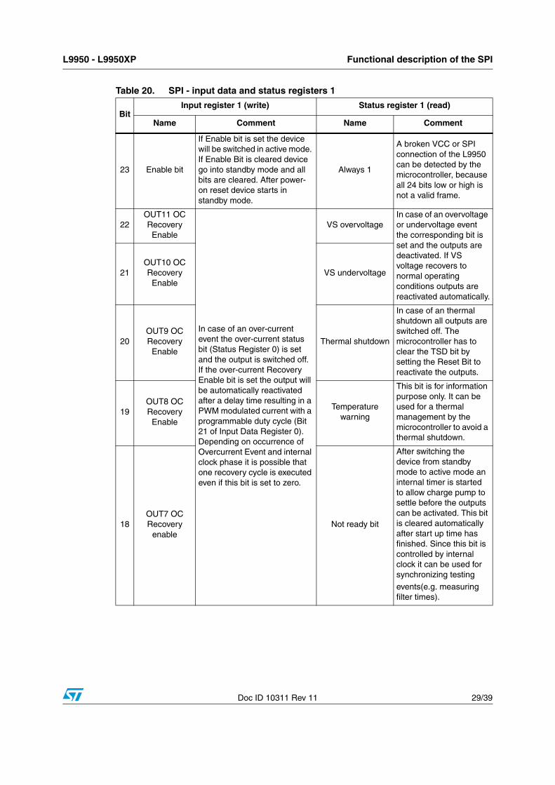
Table 20. SPI - input data and status registers 1
BitInput register 1 (write) Status register 1 (read)
Name Comment Name Comment
23 Enable bit
If Enable bit is set the device will be switched in active mode. If Enable Bit is cleared device go into standby mode and all bits are cleared. After power-on reset device starts in standby mode.
Always 1
A broken VCC or SPI connection of the L9950 can be detected by the microcontroller, because all 24 bits low or high is not a valid frame.
22OUT11 OC Recovery
Enable
In case of an over-current event the over-current status bit (Status Register 0) is set and the output is switched off. If the over-current Recovery Enable bit is set the output will be automatically reactivated after a delay time resulting in a PWM modulated current with a programmable duty cycle (Bit 21 of Input Data Register 0). Depending on occurrence of Overcurrent Event and internal clock phase it is possible that one recovery cycle is executed even if this bit is set to zero.
VS overvoltageIn case of an overvoltage or undervoltage event the corresponding bit is set and the outputs are deactivated. If VS voltage recovers to normal operating conditions outputs are reactivated automatically.
21OUT10 OC Recovery
EnableVS undervoltage
20OUT9 OC Recovery
EnableThermal shutdown
In case of an thermal shutdown all outputs are switched off. The microcontroller has to clear the TSD bit by setting the Reset Bit to reactivate the outputs.
19OUT8 OC Recovery
Enable
Temperature warning
This bit is for information purpose only. It can be used for a thermal management by the microcontroller to avoid a thermal shutdown.
18OUT7 OC Recovery
enableNot ready bit
After switching the device from standby mode to active mode an internal timer is started to allow charge pump to settle before the outputs can be activated. This bit is cleared automatically after start up time has finished. Since this bit is controlled by internal clock it can be used for synchronizing testing
events(e.g. measuring filter times).

Functional description of the SPI L9950 - L9950XP
30/39 Doc ID 10311 Rev 11
17OUT6 OC Recovery
Enable
After 50 ms the bit can be cleared. If over-current condition still exists, a wrong load can be assumed.
OUT11 – HS
open loadThe open load detection monitors the load current in each activated output stage. If the load current is below the open load detection threshold for at least 1 ms (tdOL) the corresponding open load bit is set. Due to mechanical/electrical inertia of typical loads a short activation of the outputs (e.g. 3 ms) can be used to test the open load status without changing the mechanical/electrical state of the loads.
16OUT5 OC Recovery
Enable
OUT10 – HS
open load
15OUT4 OC Recovery
Enable
OUT9 – HS open load
14OUT3 OC Recovery
Enable
OUT8 – HS
open load
13OUT2 OC Recovery
Enable
OUT7 – HS
open load
12OUT1 OC Recovery
Enable
OUT6 – HS
open load
11OUT11 PWM1
Enable
If the PWM1/2 Enable Bit is set and the output is enabled (Input Register 0) the output is switched on if PWM1/2 input is high and switched off if PWM1/2 input is low. OUT9 and OUT10 is controlled by PWM2 input all other outputs are controlled by PWM1 input.
OUT6 – LS open load
The open load detection monitors the load current in each activated output stage. If the load current is below the open load detection threshold for at least 1 ms (tdOL) the corresponding open load bit is set. Due to mechanical/electrical inertia of typical loads a short activation of the outputs (e.g. 3 ms) can be used to test the open load status without changing the mechanical/electrical state of the loads.
10OUT10 PWM2
EnableOUT5 – HS
open load
9OUT9 PWM2
EnableOUT5 – LS
open load
8OUT8 PWM1
EnableOUT4 – HS open load
7OUT7 PWM1
EnableOUT4 – LS
open load
6OUT6 PWM1
EnableOUT3 – HS
open load
5OUT4 PWM1
EnableOUT3 – LS open load
4OUT4 PWM1
EnableOUT2 –HS
open load
3OUT3 PWM1
EnableOUT2– LS
open load
2OUT4 PWM1
EnableOUT1 – HS open load
1OUT4 PWM1
EnableOUT1 – LS
open load
0 1 No Error bit
A logical NOR combination of all bits 1 to 22 in both status registers.
Table 20. SPI - input data and status registers 1 (continued)
BitInput register 1 (write) Status register 1 (read)
Name Comment Name Comment

L9950 - L9950XP Packages thermal data
Doc ID 10311 Rev 11 31/39
5 Packages thermal data
Figure 10. Packages thermal data

Package and packing information L9950 - L9950XP
32/39 Doc ID 10311 Rev 11
6 Package and packing information
6.1 ECOPACK®
In order to meet environmental requirements, ST offers these devices in different grades of ECOPACK® packages, depending on their level of environmental compliance. ECOPACK® specifications, grade definitions and product status are available at: www.st.com.
ECOPACK® is an ST trademark.
6.2 PowerSO-36 package information
Figure 11. PowerSO-36 package dimensions

L9950 - L9950XP Package and packing information
Doc ID 10311 Rev 11 33/39
Table 21. PowerSO-36 mechanical data
SymbolMillimeters
Min. Typ. Max.
A - - 3.60
a1 0.10 - 0.30
a2 - - 3.30
a3 0 - 0.10
b 0.22 - 0.38
c 0.23 - 0.32
D * 15.80 - 16.00
D1 9.40 - 9.80
E 13.90 - 14.5
E1 * 10.90 - 11.10
E2 - - 2.90
E3 5.80 - 6.20
e - 0.65 -
e3 - 11.05 -
G 0 - 0.10
H 15.50 - 15.90
h - - 1.10
L 0.8 - 1.10
M - - -
N - - 10 deg
R - - -
s - - 8 deg
Package and packing information L9950 - L9950XP
34/39 Doc ID 10311 Rev 11
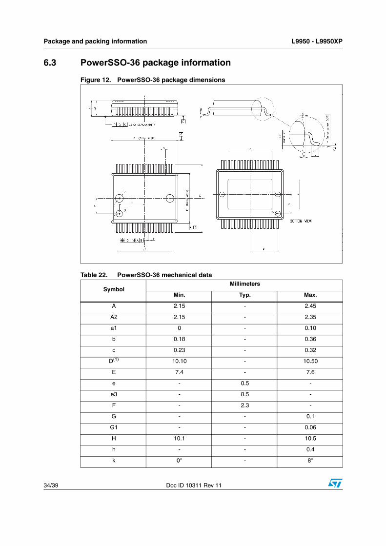
6.3 PowerSSO-36 package information
Figure 12. PowerSSO-36 package dimensions
Table 22. PowerSSO-36 mechanical data
SymbolMillimeters
Min. Typ. Max.
A 2.15 - 2.45
A2 2.15 - 2.35
a1 0 - 0.10
b 0.18 - 0.36
c 0.23 - 0.32
D(1) 10.10 - 10.50
E 7.4 - 7.6
e - 0.5 -
e3 - 8.5 -
F - 2.3 -
G - - 0.1
G1 - - 0.06
H 10.1 - 10.5
h - - 0.4
k 0° - 8°

L9950 - L9950XP Package and packing information
Doc ID 10311 Rev 11 35/39
6.4 PowerSO-36 packing information
Figure 13. PowerSO-36 tube shipment (no suffix)
L 0.55 - 0.85
M - 4.3 -
N - - 10°
O - 1.2 -
Q - 0.8 -
S - 2.9 -
T - 3.65 -
U - 1 -
X 4.3 - 5.2
Y 6.9 - 7.5
1. “D” and “E” do not include mold Flash or protrusions. Mold Flash or protrusions shall not exceed 0.15 mm per side (0.006”).
Table 22. PowerSSO-36 mechanical data (continued)
SymbolMillimeters
Min. Typ. Max.
Package and packing information L9950 - L9950XP
36/39 Doc ID 10311 Rev 11
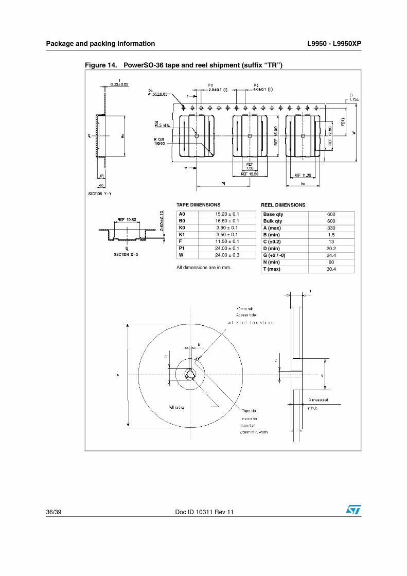
Figure 14. PowerSO-36 tape and reel shipment (suffix “TR”)
REEL DIMENSIONS
Base qty 600Bulk qty 600A (max) 330B (min) 1.5C (±0.2) 13D (min) 20.2G (+2 / -0) 24.4N (min) 60T (max) 30.4
TAPE DIMENSIONS
All dimensions are in mm.
A0 15.20 ± 0.1B0 16.60 ± 0.1K0 3.90 ± 0.1K1 3.50 ± 0.1F 11.50 ± 0.1P1 24.00 ± 0.1W 24.00 ± 0.3

L9950 - L9950XP Package and packing information
Doc ID 10311 Rev 11 37/39
6.5 PowerSSO-36 packing information
Figure 15. PowerSSO-36 tube shipment (no suffix)
Figure 16. PowerSSO-36 tape and reel shipment (suffix “TR”)
All dimensions are in mm.
Base qty 49Bulk qty 1225Tube length (±0.5) 532A 3.5B 13.8C (±0.1) 0.6
A
CB
Base qty 1000Bulk qty 1000A (max) 330B (min) 1.5C (±0.2) 13F 20.2G (+2 / -0) 24.4N (min) 100T (max) 30.4
REEL DIMENSIONS
TAPE DIMENSIONSAccording to Electronic Industries Association(EIA) Standard 481 rev. A, Feb. 1986
All dimensions are in mm.
Tape width W 24Tape hole spacing P0 (±0.1) 4Component spacing P 12Hole diameter D (±0.05) 1.55Hole diameter D1 (min) 1.5Hole position F (±0.1) 11.5Compartment depth K (max) 2.85Hole spacing P1 (±0.1) 2
Topcovertape
End
Start
No componentsNo components Components
500mm min 500mm minEmpty components pocketssealed with cover tape.
User direction of feed
Revision history L9950 - L9950XP
38/39 Doc ID 10311 Rev 11
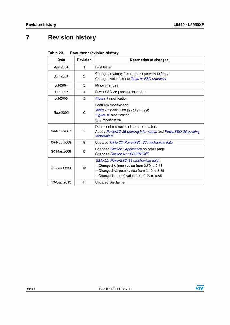
7 Revision history
Table 23. Document revision history
Date Revision Description of changes
Apr-2004 1 First Issue
Jun-2004 2Changed maturity from product preview to final;Changed values in the Table 4: ESD protection
Jul-2004 3 Minor changes
Jun-2005 4 PowerSSO-36 package insertion
Jul-2005 5 Figure 1 modification
Sep-2005 6
Features modification;Table 7 modification (ICC; IS + ICC);
Figure 10 modification;
IQLL modification.
14-Nov-2007 7Document restructured and reformatted.
Added PowerSO-36 packing information and PowerSSO-36 packing information.
05-Nov-2008 8 Updated Table 22: PowerSSO-36 mechanical data.
30-Mar-2009 9Changed Section : Application on cover page
Changed Section 6.1: ECOPACK®
09-Jun-2009 10
Table 22: PowerSSO-36 mechanical data:
– Changed A (max) value from 2.50 to 2.45– Changed A2 (max) value from 2.40 to 2.35
– Changed L (max) value from 0.90 to 0.85
19-Sep-2013 11 Updated Disclaimer.
L9950 - L9950XP
Doc ID 10311 Rev 11 39/39
Please Read Carefully:
Information in this document is provided solely in connection with ST products. STMicroelectronics NV and its subsidiaries (“ST”) reserve theright to make changes, corrections, modifications or improvements, to this document, and the products and services described herein at anytime, without notice.
All ST products are sold pursuant to ST’s terms and conditions of sale.
Purchasers are solely responsible for the choice, selection and use of the ST products and services described herein, and ST assumes noliability whatsoever relating to the choice, selection or use of the ST products and services described herein.
No license, express or implied, by estoppel or otherwise, to any intellectual property rights is granted under this document. If any part of thisdocument refers to any third party products or services it shall not be deemed a license grant by ST for the use of such third party productsor services, or any intellectual property contained therein or considered as a warranty covering the use in any manner whatsoever of suchthird party products or services or any intellectual property contained therein.
UNLESS OTHERWISE SET FORTH IN ST’S TERMS AND CONDITIONS OF SALE ST DISCLAIMS ANY EXPRESS OR IMPLIED WARRANTY WITH RESPECT TO THE USE AND/OR SALE OF ST PRODUCTS INCLUDING WITHOUT LIMITATION IMPLIED WARRANTIES OF MERCHANTABILITY, FITNESS FOR A PARTICULAR PURPOSE (AND THEIR EQUIVALENTS UNDER THE LAWS OF ANY JURISDICTION), OR INFRINGEMENT OF ANY PATENT, COPYRIGHT OR OTHER INTELLECTUAL PROPERTY RIGHT.
ST PRODUCTS ARE NOT DESIGNED OR AUTHORIZED FOR USE IN: (A) SAFETY CRITICAL APPLICATIONS SUCH AS LIFE SUPPORTING, ACTIVE IMPLANTED DEVICES OR SYSTEMS WITH PRODUCT FUNCTIONAL SAFETY REQUIREMENTS; (B) AERONAUTIC APPLICATIONS; (C) AUTOMOTIVE APPLICATIONS OR ENVIRONMENTS, AND/OR (D) AEROSPACE APPLICATIONS OR ENVIRONMENTS. WHERE ST PRODUCTS ARE NOT DESIGNED FOR SUCH USE, THE PURCHASER SHALL USE PRODUCTS AT PURCHASER’S SOLE RISK, EVEN IF ST HAS BEEN INFORMED IN WRITING OF SUCH USAGE, UNLESS A PRODUCT IS EXPRESSLY DESIGNATED BY ST AS BEING INTENDED FOR “AUTOMOTIVE, AUTOMOTIVE SAFETY OR MEDICAL” INDUSTRY DOMAINS ACCORDING TO ST PRODUCT DESIGN SPECIFICATIONS. PRODUCTS FORMALLY ESCC, QML OR JAN QUALIFIED ARE DEEMED SUITABLE FOR USE IN AEROSPACE BY THE CORRESPONDING GOVERNMENTAL AGENCY.
Resale of ST products with provisions different from the statements and/or technical features set forth in this document shall immediately voidany warranty granted by ST for the ST product or service described herein and shall not create or extend in any manner whatsoever, anyliability of ST.
ST and the ST logo are trademarks or registered trademarks of ST in various countries.Information in this document supersedes and replaces all information previously supplied.
The ST logo is a registered trademark of STMicroelectronics. All other names are the property of their respective owners.
© 2013 STMicroelectronics - All rights reserved
STMicroelectronics group of companies
Australia - Belgium - Brazil - Canada - China - Czech Republic - Finland - France - Germany - Hong Kong - India - Israel - Italy - Japan - Malaysia - Malta - Morocco - Philippines - Singapore - Spain - Sweden - Switzerland - United Kingdom - United States of America
www.st.com