Embed Size (px)
Citation preview

SUPPLEMENTARY INFORMATIONDOI: 10.1038/NMAT4143
NATURE MATERIALS | www.nature.com/naturematerials 1
Supplementary InformationUltrahigh mobility and giant magnetoresistance in Cd3As2: protection from
backscattering in a Dirac semimetal
Tian Liang1, Quinn Gibson2, Mazhar N. Ali2, Minhao Liu1, R. J. Cava2, and N. P. Ong1
Departments of Physics1 and Chemistry2, Princeton University, Princeton, NJ 08544(Dated: October 13, 2014)
PACS numbers:
S1. CRYSTAL GROWTH, EDX SPECTRA ANDX-RAY DIFFRACTION
Cd3As2 crystals were grown using excess Cd as a flux,with the overall ratio of Cd8As2. The elements werehandled in a glovebox under an Argon atmosphere andsealed in an evacuated quartz ampoule with a quartz woolplug. The sample was heated at 800 C for 2 days andthen cooled at 6 degrees per hour to 400 C, then heldfor two more days. The samples were centrifuged, andthen reheated to 400 C and centrifuged a second timeto remove excess Cd. Both needle-like (Set A) and largechunky crystals (Set B) were isolated from the resultingmaterial.
To eliminate the possibility that the very low resid-ual resistivity ρ0 observed in Set A crystals of Cd3As2is due to the presence of a thin layer of elemental Cdon the crystal surface, Energy Dispersive X-ray Spec-troscopy (EDX) analysis and Scanning Electron Micro-copy (SEM) images were taken on a FEI Quanta 200FEG Environmental SEM system. In Fig. S1, we showa small subset of the EDX spectra obtained in SamplesA1 (Panels a-d) and A2 (e and f). In order to probe thesurface composition, multiple spots on the high mobilitycrystal described here were sampled with both a 10 keVand 5 keV incident beam as well as with a 5 keV beamat the two angles of incidence, ϕ = 45 and 75. No evi-dence of any surface layer of Cd was observed. Using theKanaya-Okayama formula [1] for penetration depth, thepenetration depth of a 5 keV beam in pure Cd is about150 nm. [Using the published ρ0 of elemental Cd, 0.1-1nΩ cm, we calculate that the Cd film has to have an aver-age thickness t > 300 nm (40 nm) to mimic the observedρ0 in Sample A1 (A2).] Under these conditions, any layerof Cd would have been observed, at least, as a deviationtowards a Cd-rich stoichiometry either upon lowering thebeam energy or increasing the angle of incidence (mea-sured relative to the normal). This was not observed.In fact, a deviation towards an As-richer stoichiometrywas consistently observed at lower incident energies andhigher incident angle ϕ. Further, no features in the SEMimages of either the surface or cross section of the crystalsuggested any Cd layers or inclusions.
In addition, we searched for transport signatures ofsuperconductivity in Set A samples (Tc= 0.56 K in ele-mental Cd) in H = 0. As shown in Fig. S2, no evidencefor bulk or fluctuation superconductivity was observed
FIG. S1: EDX spectra for Samples A1 (Panels a, b, c, d)and A2 (Panels e and f). The energy of the incident beamis 5 keV (in Panels a, b, c, e, f) and 10 keV (Panel d). Wedefine the beam’s angle of incidence as ϕ. In Panels a, d, e,f, ϕ = 0 (normal incidence). In Panel b, ϕ = 45. In Panelc, ϕ = 75. The atomic percentages of As and Cd (As:Cd)in the individual panels are as follows. (a): 36.55 %: 63.45%, (b): 39.74 %: 60.26 %, (c): 47.27 %: 52.73 %, (d): 34.36%: 65.64 %, (e): 39.46 %: 60.54 %, (f): 40.44 %: 59.56% (the ideal stoichiometric ratio is 40 % : 60 %). Withinthe uncertainties, the observed spectra shift to an As-richcomposition as ϕ increases from 0→ 75 (a→b→c).
in 2 samples (A1 and A2) measured down to 0.4 K. Thisstrongly precludes either a thin surface Cd film or a bulkinclusion that extends over a significant segment of thecrystal. Finally, measurements of the SdH were taken to45 T at 0.3 K [2]. No evidence for additional SdH peakswas found (apart from the ones associated with the small
Ultrahigh mobility and giant magnetoresistance in the Dirac semimetal Cd3As2
© 2014 Macmillan Publishers Limited. All rights reserved.

2 NATURE MATERIALS | www.nature.com/naturematerials
SUPPLEMENTARY INFORMATION DOI: 10.1038/NMAT4143
2
FIG. S2: Resistivity normalized to values at 1 K in SamplesA1 (red circles) and A2 (blue circles) plotted vs. T between0.4 and 1.0 K. No signatures of bulk superconductivity or fluc-tuation superconductivity were observed in this temperatureinterval (and higher). The absence strongly argues againstthe existence of a thin film of Cd plating the crystals (or a Cdspine extending through the bulk). The critical temperatureof elemental Cd is 0.56 K.
electron pocket, as described).
Single-crystal X-ray diffraction (SXRD) was performedon a 0.04 mm × 0.04 mm × 0.4 mm crystal on aBruker APEX II diffractometer using Mo K-alpha ra-diation (lambda = 0.71073 A) at 100 K. Exposure timewas 35 seconds with a detector distance of 60 mm. Unitcell refinement and data integration were performed withBruker APEX2 software. A total of 1464 frames werecollected over a total exposure time of 14.5 hours. 21702diffracted peak observations were made, yielding 1264unique observed reflections collected over a full sphere.The crystal structure was refined using the full-matrixleast-squares method on F 2, using SHELXL2013 imple-mented through WinGX. An absorption correction wasapplied using the analytical method of De Meulenaer andTompa implemented through the Bruker APEX II soft-ware.
While the detailed SXRD measurements for structuralrefinement were carried out on small crystals, for physi-cal property measurements, larger crystals are employed.The rod characterized in this study with dimensions of0.15 mm by 0.05 mm by 1.2 mm, was used in order toascertain the growth direction of the needle (long axis).The crystal was mounted onto a flat kapton holder andthe Bruker APEX II software was used to indicate theface normals of the crystal after the unit cell and ori-entation matrix were determined. The long axis of theneedle was found to be the [110] direction. After the MRexperiments were completed, a fragment of Sample A1was also investigated by SXRD measurements and con-
FIG. S3: Single-crystal X-ray diffraction precession image ofthe 0kl plane in the reciprocal lattice of Cd3As2 obtainedon a segment (0.04 mm × 0.04 mm × 0.4 mm in size) ofSample A1. The weaker supercell reflections, which argue forthe larger tetragonal cell, may be seen in between the brightspots. No diffuse scattering is seen. All the resolved spots fitthe crystal lattice structure recently established for Cd3As2(Ref. [3]).
firmed to also have its needle axis along [110] (Fig. S3).In our experience, the very high conductivity observed
below 10 K in Set A samples degrades (albeit very slowly)when the crystals are stored at room temperature but ex-posed to ambient atmosphere. The degradation couldarise from surface oxidation or gradual changes awayfrom stoichiometry in the composition. Measurementsof ρ0 in A1 performed at NHMFL 3 months after ourin-house experiments revealed that the zero-field resid-ual resistivity ρ0 had increased from 32 nΩ cm to 110 nΩcm. This aging results in a factor of 3.45 difference inthe MR ratio ρ(H)/ρ0 measured at 1 T in the high-fieldand low-field polar plots shown in Fig. S11.
S2. MEASUREMENT OF ANISOTROPY USINGMONTGOMERTY METHOD
The Montgomery method was used to determine theanisotropy ρ2/ρ1(≡ ρy/ρx) [4]. In this method, theanisotropic solid is identified with its isotropic “equiv-alent”.
By scaling arguments, the ratio of the sample’s resis-tivities ρx and ρy is related to the isotropic equivalent’sdimensions by [4]
(ρy/ρx)1/2 = ly/lx × l/w, (S1)
where lx and ly are the (unknown) lengths along x andy axes of the isotropic equivalent, and l and w are theknown lengths of the original anisotropic sample mea-sured along its x and y axes. We need ly/lx to determinethe anisotropy.
3
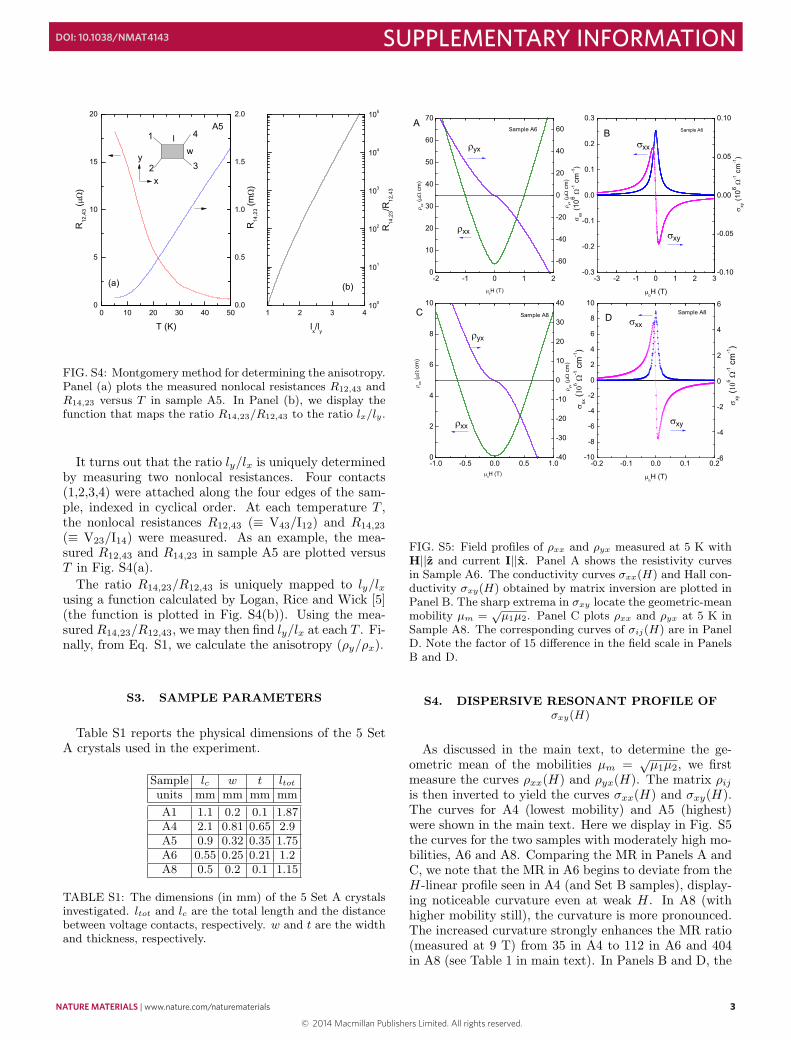
FIG. S4: Montgomery method for determining the anisotropy.Panel (a) plots the measured nonlocal resistances R12,43 andR14,23 versus T in sample A5. In Panel (b), we display thefunction that maps the ratio R14,23/R12,43 to the ratio lx/ly.
It turns out that the ratio ly/lx is uniquely determinedby measuring two nonlocal resistances. Four contacts(1,2,3,4) were attached along the four edges of the sam-ple, indexed in cyclical order. At each temperature T ,the nonlocal resistances R12,43 (≡ V43/I12) and R14,23
(≡ V23/I14) were measured. As an example, the mea-sured R12,43 and R14,23 in sample A5 are plotted versusT in Fig. S4(a).
The ratio R14,23/R12,43 is uniquely mapped to ly/lxusing a function calculated by Logan, Rice and Wick [5](the function is plotted in Fig. S4(b)). Using the mea-suredR14,23/R12,43, we may then find ly/lx at each T . Fi-nally, from Eq. S1, we calculate the anisotropy (ρy/ρx).
S3. SAMPLE PARAMETERS
Table S1 reports the physical dimensions of the 5 SetA crystals used in the experiment.
Sample lc w t ltotunits mm mm mm mm
A1 1.1 0.2 0.1 1.87A4 2.1 0.81 0.65 2.9A5 0.9 0.32 0.35 1.75A6 0.55 0.25 0.21 1.2A8 0.5 0.2 0.1 1.15
TABLE S1: The dimensions (in mm) of the 5 Set A crystalsinvestigated. ltot and lc are the total length and the distancebetween voltage contacts, respectively. w and t are the widthand thickness, respectively.
FIG. S5: Field profiles of ρxx and ρyx measured at 5 K withH||z and current I||x. Panel A shows the resistivity curvesin Sample A6. The conductivity curves σxx(H) and Hall con-ductivity σxy(H) obtained by matrix inversion are plotted inPanel B. The sharp extrema in σxy locate the geometric-meanmobility µm =
√µ1µ2. Panel C plots ρxx and ρyx at 5 K in
Sample A8. The corresponding curves of σij(H) are in PanelD. Note the factor of 15 difference in the field scale in PanelsB and D.
S4. DISPERSIVE RESONANT PROFILE OFσxy(H)
As discussed in the main text, to determine the ge-ometric mean of the mobilities µm =
√µ1µ2, we first
measure the curves ρxx(H) and ρyx(H). The matrix ρijis then inverted to yield the curves σxx(H) and σxy(H).The curves for A4 (lowest mobility) and A5 (highest)were shown in the main text. Here we display in Fig. S5the curves for the two samples with moderately high mo-bilities, A6 and A8. Comparing the MR in Panels A andC, we note that the MR in A6 begins to deviate from theH-linear profile seen in A4 (and Set B samples), display-ing noticeable curvature even at weak H. In A8 (withhigher mobility still), the curvature is more pronounced.The increased curvature strongly enhances the MR ratio(measured at 9 T) from 35 in A4 to 112 in A6 and 404in A8 (see Table 1 in main text). In Panels B and D, the
© 2014 Macmillan Publishers Limited. All rights reserved.
NATURE MATERIALS | www.nature.com/naturematerials 3
SUPPLEMENTARY INFORMATIONDOI: 10.1038/NMAT4143
3
FIG. S4: Montgomery method for determining the anisotropy.Panel (a) plots the measured nonlocal resistances R12,43 andR14,23 versus T in sample A5. In Panel (b), we display thefunction that maps the ratio R14,23/R12,43 to the ratio lx/ly.
It turns out that the ratio ly/lx is uniquely determinedby measuring two nonlocal resistances. Four contacts(1,2,3,4) were attached along the four edges of the sam-ple, indexed in cyclical order. At each temperature T ,the nonlocal resistances R12,43 (≡ V43/I12) and R14,23
(≡ V23/I14) were measured. As an example, the mea-sured R12,43 and R14,23 in sample A5 are plotted versusT in Fig. S4(a).
The ratio R14,23/R12,43 is uniquely mapped to ly/lxusing a function calculated by Logan, Rice and Wick [5](the function is plotted in Fig. S4(b)). Using the mea-suredR14,23/R12,43, we may then find ly/lx at each T . Fi-nally, from Eq. S1, we calculate the anisotropy (ρy/ρx).
S3. SAMPLE PARAMETERS
Table S1 reports the physical dimensions of the 5 SetA crystals used in the experiment.
Sample lc w t ltotunits mm mm mm mm
A1 1.1 0.2 0.1 1.87A4 2.1 0.81 0.65 2.9A5 0.9 0.32 0.35 1.75A6 0.55 0.25 0.21 1.2A8 0.5 0.2 0.1 1.15
TABLE S1: The dimensions (in mm) of the 5 Set A crystalsinvestigated. ltot and lc are the total length and the distancebetween voltage contacts, respectively. w and t are the widthand thickness, respectively.
FIG. S5: Field profiles of ρxx and ρyx measured at 5 K withH||z and current I||x. Panel A shows the resistivity curvesin Sample A6. The conductivity curves σxx(H) and Hall con-ductivity σxy(H) obtained by matrix inversion are plotted inPanel B. The sharp extrema in σxy locate the geometric-meanmobility µm =
√µ1µ2. Panel C plots ρxx and ρyx at 5 K in
Sample A8. The corresponding curves of σij(H) are in PanelD. Note the factor of 15 difference in the field scale in PanelsB and D.
S4. DISPERSIVE RESONANT PROFILE OFσxy(H)
As discussed in the main text, to determine the ge-ometric mean of the mobilities µm =
√µ1µ2, we first
measure the curves ρxx(H) and ρyx(H). The matrix ρijis then inverted to yield the curves σxx(H) and σxy(H).The curves for A4 (lowest mobility) and A5 (highest)were shown in the main text. Here we display in Fig. S5the curves for the two samples with moderately high mo-bilities, A6 and A8. Comparing the MR in Panels A andC, we note that the MR in A6 begins to deviate from theH-linear profile seen in A4 (and Set B samples), display-ing noticeable curvature even at weak H. In A8 (withhigher mobility still), the curvature is more pronounced.The increased curvature strongly enhances the MR ratio(measured at 9 T) from 35 in A4 to 112 in A6 and 404in A8 (see Table 1 in main text). In Panels B and D, the
© 2014 Macmillan Publishers Limited. All rights reserved.

4 NATURE MATERIALS | www.nature.com/naturematerials
SUPPLEMENTARY INFORMATION DOI: 10.1038/NMAT41434
FIG. S6: Tracking the change in mobility versus T in SampleA5. Panel A plots the mobilities µ1 and µm versus the zero-field conductivity σ0
1 in A5 with T as the parameter. As Tis lowered to 5 K, values of µm inferred from the peak fieldin σxy track very well the increase in σ0
1 ; the mobility µ1 –
calculated from µm(T )√
γ(T ) – attains a value close to 107
cm2/Vs. Panel B shows the curves of σxy(H) at selected Tfrom 5 to 60 K. Because of the large variation in peak valuesof σxy, each curve has been multiplied by the vertical scalefactor indicated. The peak fields, equal to µ−1
m , shift veryrapidly to very small values as T decreases to 5 K.
curves of σxy(H) display the “dispersion-resonance” pro-file as discussed, with sharp peaks at fields which locatethe value 1/µm. Going from A6 (Panel B) to A8 (PanelD), the mobility µ1 increases by a factor of 12.5. Thiscauses the peaks to move in by the same factor (note thedifference in field scales).
To check that the peak field in σxy accurately measuresthe mobility µm, we can follow the peak field as T isincreased in one sample. Figure S6A shows that bothµm(T ) and µ1(T ) measured in Sample A5 track closelyits zero-H conductivity σ0
1 as T varies from 100 K to 5 K(µ1 = µm
√γ). Panel B shows the curves of σxy(H) for
selected T between 5 and 60 K. The peak values of σxy
vary by over 2 orders of magnitude in this range of T .Hence, we have multiplied each curve by an appropriatescale factor to make them resolvable.
FIG. S7: Comparison of the normalized Hall conductivityσxy(H)/σmax
xy vs. the scaled field B/Bmax in Samples A4,A5, A6 and A8. The scaled form of the Hall conductivity isnominally similar despite a 100-fold change in both Bmax andσmax.
Non-uniformity concern and scaling plotsA concern is whether the observed low residual resis-tivity ρ1 (21 nΩcm) could arise from a strongly inho-mogeneous distribution of lifetimes in the sample. Theresonant nature of the peaks in σxy(H) can directly ad-dress this issue. In analogy with inhomogeneous broad-ening in NMR, we expect that a broad distribution oflifetimes (hence mobilities) will also broaden the peakin σxy in proportion. If the increase in conductivity σ0
1
(from A4 to A5) is caused by having local regions with avery broad distribution of transport lifetimes, one shouldsee a comparable distribution of peak fields contributingto the measured σxy(H) profile.
This is not observed. In terms of rescaled variables,we plot the normalized curve σxy(H)/σmax
xy vs. B/Bmax
where σmaxxy is the Hall conductivity value at the peak
field Bmax for 4 Set A samples. Within the experimentaluncertainty, the widths collapse to the same curve de-spite a 100-fold change in Bmax. The evidence is that, asµm increases 100-fold (as tracked by the peak), the formof the σxy profile remains unchanged after appropriaterescaling of the field axis; the distribution of mobilitiesremains very narrow. We argue that this is direct evi-dence against a broad distribution of lifetimes appearingin the high-mobility samples.
S5. HIGH MOBILITY: COMPARISON WITHBISMUTH AND 2DEG IN GAAS/ALGAAS
It is interesting to compare the ultrahigh values at-tained by the mobility µ1 (∼ 9× 106 cm2/Vs) with mo-bilities in in the purest bismuth samples and in the bestsamples of 2DEG confined in GaAs/AsGaAs quantumwells. There is some spread in the reported mobility
5
values in Bi because both the mobilities of the electronand hole pockets (µn and µp) are highly anisotropic. In-cluding values along the 3 axes, there are altogether 6values of the mobilities to be determined. This is doneby fitting extensive magnetoresistance measurements toa Boltzmann-equation model [6–8]. Most reports obtainvalues µn in the range 1-10 million cm2/Vs. The highestvalue is 90 million cm2/Vs reported from a fit by Hart-man [8]. (By contrast, the values in Cd3As2 reportedhere are directly measured from the peaks in σxy as ex-plained above.)
The mobilities in 2DEG in GaAs/AlGaAs heterostruc-tures are more reliably determined experimentally sincethe single FS is isotropic and the carrier density is knownto very high accuracy. As reported in Ref. [9], the high-est value is 36 million cm2/Vs.
A key point is that, in the “ideal” Cd3As2 lattice, thereare 64 sites for the Cd ions in each unit cell, and that ex-actly 1
4 of the sites are vacant. From the large variation ofthe RRR (20→4,100) in Set A crystals extracted from thesame boule, we infer that the vacancy sites are orderedwith a correlation length ξ that varies strongly acrosscrystals grown under nominally similar conditions (thelargest RRR is obtained with the longest ξ). This dis-order leads to strong reduction of the quantum lifetimeτQ derived from damping of the SdH oscillations. Weremark that neither Bi nor the 2DEG in GaAs/AlGaAssuffer from this type of vacancy disorder (Bi has only 2atoms per unit cell). Thus it is noteworthy that µ1 inCd3As2 attains values nearly comparable to the mobili-ties in the best Bi and 2DEG samples.
As described in the main text, the transport lifetimeτtr (which determines the mobility) can be longer thanτQ by factors of Rτ ≃ 104 in Cd3As2. The lattice disorderleads to predominantly forward scattering, but has nearlyno effect in relaxing the forward drift velocity. To us,this suggests the existence of strong protection againstbackscattering, by an unknown mechanism. In the caseof 2DEG in GaAs/AlGaAs, Rτ is also very large (102),but the reason there is now well-understood [10–12]. Bydelta-doping, the doped charge impurities are set backfrom the 2DEG by 1 micron. The gentle residual disorderseen by electrons in the 2DEG only causes small-anglescattering.
S6. SDH FITS AND SEARCH FOR A SECONDBAND
Figure S8 plots the SdH curves together with fits tothe standard Lifshitz-Kosevich expression in Sample B7for θ = 0, 4, -4. We used the Lifshitz-Kosevich (LK)expression in the form
∆Gxx
Gxx=
(ωc
2EF
)1/2λ
sinhλe−λD cos
(πk2FeB
+ φ
)
(S2)
FIG. S8: (Panel a) Fits of ρxx vs. H to the LK expression(dashed curves) at selected θ (0, ±4) in Sample B7 at 2.5 K.Panel (b) plots the curve and fit at θ = 0 versus 1/B to showthe exponential damping of the amplitude. (Panel c) The fitto the amplitude at B = 5.9 T vs. T yields the effective mass(or equivalently, the Fermi velocity vF = 9.3×10⁵ m/s).
with λ = 2π2kBT/ωc and λD = 2π2kBTD/ωc, whereωc = eB/mc is the cyclotron frequency, with mc thecyclotron mass. The Dingle temperature is given byTD = /(2πkBτQ), with τQ the quantum lifetime. Forthe Dirac dispersion in Cd3As2, the cyclotron mass isgiven by mc = EF /v
2F .
To isolate the oscillatory component in each curve ofρxx vs. H, we first determine the strongly H-dependent“background” ρave by averaging out the sinusoidal oscil-lations (the curve ρave at θ = 0 is plotted in Fig. 4d inthe main text). After this background is removed, we areleft with the purely sinusoidal component which is expo-nentially damped vs. 1/H (inset in Fig. S8). This maybe fitted to the LK expression by a least-squares fit rou-tine. In general, very close fits to all the observed curvesare achieved, as shown (after restoring the background)in Fig. S8 for Sample B7 (see Fig. 4B in the main textfor A1). The lower panel shows the T dependence of theSdH oscillation amplitude at B = 5.9 T. By fitting toEq. S2 (red curve), we determine mc. From the fits, weobtain SF= 44 T, EF = 220 meV, vF = 9.3×10⁵ m/s,τQ = 5.1×10⁻¹⁴ s.
Is there a second band?
© 2014 Macmillan Publishers Limited. All rights reserved.

NATURE MATERIALS | www.nature.com/naturematerials 5
SUPPLEMENTARY INFORMATIONDOI: 10.1038/NMAT41435
values in Bi because both the mobilities of the electronand hole pockets (µn and µp) are highly anisotropic. In-cluding values along the 3 axes, there are altogether 6values of the mobilities to be determined. This is doneby fitting extensive magnetoresistance measurements toa Boltzmann-equation model [6–8]. Most reports obtainvalues µn in the range 1-10 million cm2/Vs. The highestvalue is 90 million cm2/Vs reported from a fit by Hart-man [8]. (By contrast, the values in Cd3As2 reportedhere are directly measured from the peaks in σxy as ex-plained above.)
The mobilities in 2DEG in GaAs/AlGaAs heterostruc-tures are more reliably determined experimentally sincethe single FS is isotropic and the carrier density is knownto very high accuracy. As reported in Ref. [9], the high-est value is 36 million cm2/Vs.
A key point is that, in the “ideal” Cd3As2 lattice, thereare 64 sites for the Cd ions in each unit cell, and that ex-actly 1
4 of the sites are vacant. From the large variation ofthe RRR (20→4,100) in Set A crystals extracted from thesame boule, we infer that the vacancy sites are orderedwith a correlation length ξ that varies strongly acrosscrystals grown under nominally similar conditions (thelargest RRR is obtained with the longest ξ). This dis-order leads to strong reduction of the quantum lifetimeτQ derived from damping of the SdH oscillations. Weremark that neither Bi nor the 2DEG in GaAs/AlGaAssuffer from this type of vacancy disorder (Bi has only 2atoms per unit cell). Thus it is noteworthy that µ1 inCd3As2 attains values nearly comparable to the mobili-ties in the best Bi and 2DEG samples.
As described in the main text, the transport lifetimeτtr (which determines the mobility) can be longer thanτQ by factors of Rτ ≃ 104 in Cd3As2. The lattice disorderleads to predominantly forward scattering, but has nearlyno effect in relaxing the forward drift velocity. To us,this suggests the existence of strong protection againstbackscattering, by an unknown mechanism. In the caseof 2DEG in GaAs/AlGaAs, Rτ is also very large (102),but the reason there is now well-understood [10–12]. Bydelta-doping, the doped charge impurities are set backfrom the 2DEG by 1 micron. The gentle residual disorderseen by electrons in the 2DEG only causes small-anglescattering.
S6. SDH FITS AND SEARCH FOR A SECONDBAND
Figure S8 plots the SdH curves together with fits tothe standard Lifshitz-Kosevich expression in Sample B7for θ = 0, 4, -4. We used the Lifshitz-Kosevich (LK)expression in the form
∆Gxx
Gxx=
(ωc
2EF
)1/2λ
sinhλe−λD cos
(πk2FeB
+ φ
)
(S2)
FIG. S8: (Panel a) Fits of ρxx vs. H to the LK expression(dashed curves) at selected θ (0, ±4) in Sample B7 at 2.5 K.Panel (b) plots the curve and fit at θ = 0 versus 1/B to showthe exponential damping of the amplitude. (Panel c) The fitto the amplitude at B = 5.9 T vs. T yields the effective mass(or equivalently, the Fermi velocity vF = 9.3×10⁵ m/s).
with λ = 2π2kBT/ωc and λD = 2π2kBTD/ωc, whereωc = eB/mc is the cyclotron frequency, with mc thecyclotron mass. The Dingle temperature is given byTD = /(2πkBτQ), with τQ the quantum lifetime. Forthe Dirac dispersion in Cd3As2, the cyclotron mass isgiven by mc = EF /v
2F .
To isolate the oscillatory component in each curve ofρxx vs. H, we first determine the strongly H-dependent“background” ρave by averaging out the sinusoidal oscil-lations (the curve ρave at θ = 0 is plotted in Fig. 4d inthe main text). After this background is removed, we areleft with the purely sinusoidal component which is expo-nentially damped vs. 1/H (inset in Fig. S8). This maybe fitted to the LK expression by a least-squares fit rou-tine. In general, very close fits to all the observed curvesare achieved, as shown (after restoring the background)in Fig. S8 for Sample B7 (see Fig. 4B in the main textfor A1). The lower panel shows the T dependence of theSdH oscillation amplitude at B = 5.9 T. By fitting toEq. S2 (red curve), we determine mc. From the fits, weobtain SF= 44 T, EF = 220 meV, vF = 9.3×10⁵ m/s,τQ = 5.1×10⁻¹⁴ s.
Is there a second band?
© 2014 Macmillan Publishers Limited. All rights reserved.

6 NATURE MATERIALS | www.nature.com/naturematerials
SUPPLEMENTARY INFORMATION DOI: 10.1038/NMAT41436
FIG. S9: High-field SdH oscillations in Cd3As2. Panel A plotsthe trace of the longitudninal MR ρxx vs. H up to field 45T taken in Sample A12 at T = 0.35 K (with θ = 0 ± 5).The integers indicate the LL index inferred from Panel B. Theinset shows the plot of the ratio ∆ρxx(H)/ρxx (solid curve)after a smooth background curve is subtracted to isolate theSdH oscillations. From the fit to the LK expression (dashedcurve) we obtain a quantum lifetime τQ = 8.56 × 10⁻¹⁴ s.Panel B is the index plot identifying the index of each Landaulevel from the maxima in ∆ρxx. The N=1 level is reached at27 T. The existence of a second high-mobility band with adifferent period can be excluded to a resolution of 3%.
To check whether a second band of carriers is present,we have extended the SdH measurements to DC fieldsof 45 T. Results on a new Set A sample A12 (residualresistivity ρ1 = 180 nΩcm in zero H) are shown in Fig.S9. Panel A plots the longitudinal MR taken at T =0.35 K in a field nominally along the needle axis (θ =0±5). SdH oscillations are strongest in the longitudinalMR geometry. After subtracting a smooth background,the SdH oscillations can be fit to the LK expression toyield SF = 40.5 T (inset). Panel B shows the “index”plot of the integers N vs. 1/BN where BN are the fieldsat which ∆ρxx attains a maximum. The N = 1 level isreached at 27 T. For fields above the last minimum (at36 T), we begin to access the N=0 LL (quantum limit).
If another FS pocket is present with mobility exceeding∼ 2×103 cm2/Vs, its SdH peaks should be visible in thetraces of ρxx and ∆ρxx, and display a period (vs. 1/B)distinct from the dominant oscillation, especially in fields
FIG. S10: Polar plot of the angular variation of the low-T MR(in Sample B7) for H fixed at values 0.1,· · · , 0.3 T. The radialcoordinate represents the ratio ρxx(H)/ρ0 (with values shownon the left axis), and the angular coordinate is the tilt angle θof H. As H → 0, the MR becomes isotropic, suggesting thatthe weak-H MR is mediated by the spin degrees.
above 30 T. To a resolution 3% of the amplitude of thedominant oscillation, we do not resolve a second band orFS pocket.
The STM experiment [13], which resolves peaks in thedensity of states of LLs in fields up to 14 T using QPI(quasiparticle interference), was performed on a crystalextracted from the same flux boule. The QPI resultsalso see only one electron band. Based on results fromthe two very different experiments on samples extractedfrom the same growth boule, we can exclude the existenceof a second FS pocket distinct from the dominant one.
S7. CHIRAL ANOMALY
An interesting prediction in Weyl semimetals is theeffect of the “chiral anomaly” on transport [14–16]. In amagnetic field B||z, each Dirac node is predicted to splitinto two Weyl nodes with opposite chirality χ = ±1. Thelowest Landau level (LL) in each Weyl node displays a
linear dispersion along B with the sign fixed by χ, i.e.the energy of the lowest LL is given by E0 = −χvF kzwhere vF is the Fermi velocity. In an electric field E,charge Q is pumped between the two branches at the rate
Q = −V e3
4π22E·B, with V the volume of the sample [14].In the quantum limit (only lowest LL occupied), the
charge pumping yields a conductivity increment givenby [15, 16]
δσzz =1
(2π)2e3
2BvF τv, (S3)
where τv is the intervalley relaxation time. Using themobility µ = evF τtr/kF , we may write the ratio of the
7
FIG. S11: Polar plot of the angular variation of the low-TMR (Sample A1) in high fields, 10-34.5 T (upper panel) andin very weak H (≤0.5 T, lower panel). The radial coordinaterepresents the ratio ρxx(H)/ρ0 (with values shown on the leftaxis). The angular coordinate is the tilt angle θ of H. ForH <0.1 T, the MR is nearly isotropic, but acquires a dipolarcomponent that grows rapidly as H increases. The weak-field,isotropic regime in Set A samples is confined to very weak H,and difficult to investigate compared with Set B samples. Thehigh-field polar plot was acquired 3 months after the low-fieldresults. There is a factor of 3.45 difference between the twopolar plots because ρ0 increased from 32 to 110 nΩcm pre-sumably from aging processes during the intervening period(see text).
chiral term to the zero-H conductivity as
δσzz
σ(0)=
3
4
1
(kF ℓB)2τvτtr
, (S4)
where ℓB =√
/eB is the magnetic length. For Sam-ple B7, the ratio comes out to ∼ (B/100)(τv/τtr). As arough estimate of the size of the contribution, we maycrudely assume that τv ∼ τtr. The chiral term then givesa negative MR of about 1 % at 1 T.
S8. POLAR PLOTS
Figure S10 shows the polar plots of Sample B7 atlow field (< 0.3 T). The observed MR becomes nearly
FIG. S12: The effect of varying T (2.5→ 300 K) on the MRin Sample B1. Panel A plots the MR curves ρxx vs. H atfixed T with θ = 90. An expanded view of the low H regionis given in the inset. In Panel B, we plot the T dependenceof ρxx(T,H) with H fixed at selected values. For H > 2 T,the curves are nearly T independent.
isotropic below 0.3 T. This implies that the MR is me-diated by the spin degrees through the Zeeman term.Above 0.3 T, the contribution of the orbital degrees be-come increasingly important, and the polar plot assumesa dipolar pattern.
A similar crossover is seen in Sample A1. However, be-cause of the high mobility, the crossover occurs at weakerH (< 0.1 T). Figure S11a shows the dipolar pattern inhigh fields (H > 10 T). In the limit of weak H (Panel b),the pattern crosses over to a nearly isotropic form below0.1 T.
S9. TEMPERATURE DEPENDENCE ANDLONGITUDINAL MR
The large transverse MR extends to 300 K. FigureS12A plots curves of ρxx(T,H) in Sample B1 (θ = 90)at several temperatures. As T is increased from 2.5 to300 K, the MR profile is nominally unchanged exceptthat the parabolic variation in weak H becomes moreevident (we show the minima on expanded scale in theinset). We observe that ρxx(T,H) is nominally T inde-pendent above 2 T. The effect of T is pronounced in weak
© 2014 Macmillan Publishers Limited. All rights reserved.

NATURE MATERIALS | www.nature.com/naturematerials 7
SUPPLEMENTARY INFORMATIONDOI: 10.1038/NMAT4143 7
FIG. S11: Polar plot of the angular variation of the low-TMR (Sample A1) in high fields, 10-34.5 T (upper panel) andin very weak H (≤0.5 T, lower panel). The radial coordinaterepresents the ratio ρxx(H)/ρ0 (with values shown on the leftaxis). The angular coordinate is the tilt angle θ of H. ForH <0.1 T, the MR is nearly isotropic, but acquires a dipolarcomponent that grows rapidly as H increases. The weak-field,isotropic regime in Set A samples is confined to very weak H,and difficult to investigate compared with Set B samples. Thehigh-field polar plot was acquired 3 months after the low-fieldresults. There is a factor of 3.45 difference between the twopolar plots because ρ0 increased from 32 to 110 nΩcm pre-sumably from aging processes during the intervening period(see text).
chiral term to the zero-H conductivity as
δσzz
σ(0)=
3
4
1
(kF ℓB)2τvτtr
, (S4)
where ℓB =√
/eB is the magnetic length. For Sam-ple B7, the ratio comes out to ∼ (B/100)(τv/τtr). As arough estimate of the size of the contribution, we maycrudely assume that τv ∼ τtr. The chiral term then givesa negative MR of about 1 % at 1 T.
S8. POLAR PLOTS
Figure S10 shows the polar plots of Sample B7 atlow field (< 0.3 T). The observed MR becomes nearly
FIG. S12: The effect of varying T (2.5→ 300 K) on the MRin Sample B1. Panel A plots the MR curves ρxx vs. H atfixed T with θ = 90. An expanded view of the low H regionis given in the inset. In Panel B, we plot the T dependenceof ρxx(T,H) with H fixed at selected values. For H > 2 T,the curves are nearly T independent.
isotropic below 0.3 T. This implies that the MR is me-diated by the spin degrees through the Zeeman term.Above 0.3 T, the contribution of the orbital degrees be-come increasingly important, and the polar plot assumesa dipolar pattern.
A similar crossover is seen in Sample A1. However, be-cause of the high mobility, the crossover occurs at weakerH (< 0.1 T). Figure S11a shows the dipolar pattern inhigh fields (H > 10 T). In the limit of weak H (Panel b),the pattern crosses over to a nearly isotropic form below0.1 T.
S9. TEMPERATURE DEPENDENCE ANDLONGITUDINAL MR
The large transverse MR extends to 300 K. FigureS12A plots curves of ρxx(T,H) in Sample B1 (θ = 90)at several temperatures. As T is increased from 2.5 to300 K, the MR profile is nominally unchanged exceptthat the parabolic variation in weak H becomes moreevident (we show the minima on expanded scale in theinset). We observe that ρxx(T,H) is nominally T inde-pendent above 2 T. The effect of T is pronounced in weak
© 2014 Macmillan Publishers Limited. All rights reserved.

8 NATURE MATERIALS | www.nature.com/naturematerials
SUPPLEMENTARY INFORMATION DOI: 10.1038/NMAT4143
8
FIG. S13: Panel a (upper panel) plots the MR curves ρxx vs.H at selected field-tilt angles θ at 300 K in Sample B7. As Tincreases from 2.5 to 300 K, the zero-H value of ρxx increasesby a factor of 7.7. However, at large H (e.g. 9 T), ρxx ≃1.8mΩcm is nearly the same as at 2.5 K. The broadening atH=0 is closely similar to that observed in Sample B1. InPanel b (lower panel), we plot the longitudinal (θ = 0) MRcurves as T is reduced from 300 K to 2.5 K. Below 60 K, SdHoscillations become resolvable. As T →2.5 K, a negative MRterm can be resolved as a slight decrease in the backgroundcurve (when the SdH oscillations are averaged out).
H but becomes insignificant at large H. In Panel B, wehave replotted the data in Panel A as ρxx vs. T with Hfixed at selected values. Whereas at H = 0, the profileis strongly metallic, it rapidly becomes T independentwhen H exceeds 2 T. This behavior should be contrastedwith what is observed in Bi where the fixed-field curvesretain strong T dependence even when H is very large.
In Fig. S13a, we keep T fixed at 300 K (data fromSample B7), but rotate θ from 90 to 0. As discussed inthe main text, the MR ratio measured at 2.5 K is stronglysuppressed when θ → 0. The pattern at 300 K is simi-lar (except that the minimum at H = 0 is significantlyrounded as the mobility decreases).
Finally, we show how raising T affects the small neg-ative MR contribution observed in a longitudinal H (seeρave in Fig. 4B of the main text). With θ fixed at 0, wewarm up the sample to 300 K. The SdH oscillation ampli-tude is suppressed above 40 K. Significantly, above 20 K,the negative MR term rapidly becomes unresolvable. At300 K, the longitudinal MR is strongly positive. Theseplots show that the negative MR is a low-temperaturefeature that is easily suppressed above 20 K.
We thank Andrei Bernevig, Sid Parameswaran, AshvinVishwanath and Ali Yazdani for valuable discussions, andNan Yao for assistance with the EDX. N.P.O. is sup-ported by the Army Research Office (ARO W911NF-11-1-0379). R.J.C. and N.P.O. are supported by fundsfrom a MURI grant on Topological Insulators (AROW911NF-12-1-0461) and the US National Science Foun-dation (grant number DMR 0819860). T.L acknowledgesscholarship support from the Japan Student Services Or-ganization. Some of the experiments were performed atthe National High Magnetic Field Laboratory, which issupported by National Science Foundation CooperativeAgreement No. DMR-1157490, the State of Florida, andthe U.S. Department of Energy.
[1] K. Kanaya and S. Okayama, “Penetration and Energy-Loss Theory of Electrons in Solid Targets,” J Phys DAppl Phys 5, 43 (1972).
[2] Tian Liang et al., to be published.[3] Mazhar N. Ali, Quinn Gibson, Sangjun Jeon, Brian B.
Zhou, Ali Yazdani, and R. J. Cava, “The Crystal andElectronic Structures of Cd3As2, the Three-DimensionalElectronic Analogue of Graphene,” Inorg Chem 53, 4062-4067 (2014).
[4] H. C. Montgomery, “Method for Measuring Electrical Re-sistivity of Anisotropic Materials,” J Appl Phys 42, 2971(1971).
[5] B. F. Logan, S. O. Rice, and R. F. Wick, “Series forcomputing current flow in a rectangular block,” J ApplPhys 42, 2975 (1971).
[6] Shoichi Mase, S. von Molnar and A. W. Lawson, “Gal-vanomagnetic Tensor of Bismuth at 20.4 K,” Phys. Rev.127, 1030 (1962).
9
[7] R. N. Bhargava, “de-Haas van Alphen and Galvanomag-netic Effect in Bi and Bi-Pd Alloys,” Phys. Rev. 156, 785(1967).
[8] Robert Hartman, “Temperature Dependence of the Low-Field Galvanomagnetic Coefficients of Bismuth,” Phys.Rev. 181, 1070 (1969).
[9] Darrell G. Schlom and Loren N. Pfeiffer, “Upward mo-bility rocks!” Nature Materials 9, 881 (2010).
[10] M. A. Paalanen, D. C. Tsui and J. C. M. Hwang,“Parabolic Magnetoresistance from the Interaction Effectin a Two-Dimensional Electron-Gas,” Phys Rev Lett 51,2226-2229 (1983).
[11] J. P. Harrang, R. J. Higgins, R. K. Goodall, P. R. Jay, M.Laviron and P. Delescluse, “Quantum and Classical Mo-bility Determination of the Dominant Scattering Mech-anism in the Two-Dimensional Electron-Gas of an Al-GaAs/GaAs Heterojunction,” Phys Rev B 32, 8126-8135(1985).
[12] P. T. Coleridge, “Small-Angle Scattering in 2-Dimensional Electron Gases,” Phys Rev B 44, 3793-3801(1991).
[13] Sangjun Jeon et al., “Landau Quantization and Quasi-particle Interference in the Three-Dimensional DiracSemimetal Cd3As2,” Nat. Mater., in press, cond-matarXiv:1403.3446
[14] Pavan Hosur, Xiaoliang Qi, “Recent developments intransport phenomena in Weyl semimetals,” ComptesRendus Physique, 14, 857 (2013)
[15] H. B. Nielsen and M. Ninomiya, “The Adler-Bell-JackiwAnomaly and Weyl Fermions in a Crystal,” Phys Lett B130, 389-396 (1983).
[16] D. T. Son and B. Z. Spivak, “Chiral anomaly and classicalnegative magnetoresistance of Weyl metals,” Phys. Rev.B 88, 104412 (2013)
© 2014 Macmillan Publishers Limited. All rights reserved.

NATURE MATERIALS | www.nature.com/naturematerials 9
SUPPLEMENTARY INFORMATIONDOI: 10.1038/NMAT4143
9
[7] R. N. Bhargava, “de-Haas van Alphen and Galvanomag-netic Effect in Bi and Bi-Pd Alloys,” Phys. Rev. 156, 785(1967).
[8] Robert Hartman, “Temperature Dependence of the Low-Field Galvanomagnetic Coefficients of Bismuth,” Phys.Rev. 181, 1070 (1969).
[9] Darrell G. Schlom and Loren N. Pfeiffer, “Upward mo-bility rocks!” Nature Materials 9, 881 (2010).
[10] M. A. Paalanen, D. C. Tsui and J. C. M. Hwang,“Parabolic Magnetoresistance from the Interaction Effectin a Two-Dimensional Electron-Gas,” Phys Rev Lett 51,2226-2229 (1983).
[11] J. P. Harrang, R. J. Higgins, R. K. Goodall, P. R. Jay, M.Laviron and P. Delescluse, “Quantum and Classical Mo-bility Determination of the Dominant Scattering Mech-anism in the Two-Dimensional Electron-Gas of an Al-GaAs/GaAs Heterojunction,” Phys Rev B 32, 8126-8135(1985).
[12] P. T. Coleridge, “Small-Angle Scattering in 2-Dimensional Electron Gases,” Phys Rev B 44, 3793-3801(1991).
[13] Sangjun Jeon et al., “Landau Quantization and Quasi-particle Interference in the Three-Dimensional DiracSemimetal Cd3As2,” Nat. Mater., in press, cond-matarXiv:1403.3446
[14] Pavan Hosur, Xiaoliang Qi, “Recent developments intransport phenomena in Weyl semimetals,” ComptesRendus Physique, 14, 857 (2013)
[15] H. B. Nielsen and M. Ninomiya, “The Adler-Bell-JackiwAnomaly and Weyl Fermions in a Crystal,” Phys Lett B130, 389-396 (1983).
[16] D. T. Son and B. Z. Spivak, “Chiral anomaly and classicalnegative magnetoresistance of Weyl metals,” Phys. Rev.B 88, 104412 (2013)
© 2014 Macmillan Publishers Limited. All rights reserved.