Embed Size (px)
Citation preview
March 2005
Slide 1
doc.: IEEE 15-05-0132-02-004a
Submission SAIT/IRE/SEM/DM/ETRI/KAIST/HGU/SFU/Inha
Project: IEEE P802.15 Working Group for Wireless Personal Area NProject: IEEE P802.15 Working Group for Wireless Personal Area Networks (WPANs)etworks (WPANs)
Submission Title: [Merged Proposal of Chaotic UWB System for 802.15.4a]Date Submitted: [March 7, 2005]Source: [(1) Young-Hwan Kim, Jae-Hyon Kim, Chia-Chin Chong, Su Khiong Yong, Seong-Soo Lee, (2) Hyung Soo Lee, Cheol Hyo Lee, (3) Jeongsuk Lee, (4) Namhyong Kim, (5) Kyung Sup Kwak, (6) A. S. Dmitriev, A. I. Panas, S. O. Starkov, Yu. V. Andreyev, E. V. Efremova, L. V. Kuzmin, (7) Haksun Kim, (8) Jaesang Cha, (9) Dong Jo Park, Dan Keun Sung, Sung Yoon Jung, Chang Yong Jung, (10) Joon Yong Lee, (11) Dong In Kim, Serhat Erküçük]Company: [(1) Samsung Electronics Co., Ltd. (Samsung Advanced Institute of Technology (SAIT)), (2) Electronics and Telecommunications Research Institute (ETRI), (3) Samsung Electro-Mechanics Co., Ltd. (SEM), (4) Samsung Electronics (DM), (5) UWB-ITRC, Inha University, (6) Institute of Radio Engineering and Electronics (IRE), (7) Hanbat Univ., (8) Seokyeong Univ., (9) Korea Advanced Institute of Science and Technologies (KAIST), (10) Handong Global University (HGU), (11) Simon Fraser University] E-Mail: [(1) [email protected], (2) [email protected], (3) [email protected], (4) [email protected], (5) [email protected], (6) [email protected], (7) [email protected], (8) [email protected], (9) [email protected], (10) [email protected], (11) [email protected]]
Re: [Response to IEEE 802.15.4a Call for Proposals (04/380r2)]Abstract: [Proposal for the IEEE 802.15.4a PHY standard based on the chaotic UWB system technology.]Purpose: [Proposal for the IEEE 802.15.4a PHY standard.]
Notice: This document has been prepared to assist the IEEE P802.15. It is offered as a basis for discussion and is not binding on the contributing individual(s) or organization(s). The material in this document is subject to change in form and content after further study. The contributor(s) reserve(s) the right to add, amend or withdraw material contained herein.Release: The contributor acknowledges and accepts that this contribution becomes the property of IEEE and may be made publicly available by P802.15.
doc.: IEEE 15-05-0132-01-004a
Submission Slide 2 SAIT/IRE/SEM/DM/ETRI/KAIST/HGU/SFU/Inha
March 2005
Samsung Electronics (SAIT)/IRE/Samsung Electro-Mechanics(SEM), Samsung Electronics (DM),
Electronics and Telecommunications Research Institute(ETRI)/KAIST/HGU, Simon Fraser University(SFU)/Inha University,
Chaotic UWB System
Young-Hwan Kim, Jae-Hyon Kim, Chia-Chin Chong, Su Khiong Yong, Seong-Soo Lee,A. S. Dmitriev, A. I. Panas, S. O. Starkov, Yu. V. Andreyev, E. V. Efremova, L. V. Kuzmin, Jeongsuk Lee, Haksun Kim, Jaesang Cha, Namhyong Kim, Haksun Kim, Jaesang Cha,
Hyung Soo Lee, Cheol Hyo Lee, Dong Jo Park, Dan Keun Sung , Sung Yoon Jung, Chang Yong Jung, Joon Yong Lee, Dong In Kim, Serhat Erküçük, Kyung Sup Kwak
March 2005
Slide 3
doc.: IEEE 15-05-0132-02-004a
Submission SAIT/IRE/SEM/DM/ETRI/KAIST/HGU/SFU/Inha
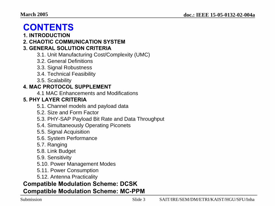
CONTENTS1. INTRODUCTION2. CHAOTIC COMMUNICATION SYSTEM3. GENERAL SOLUTION CRITERIA
3.1. Unit Manufacturing Cost/Complexity (UMC)3.2. General Definitions3.3. Signal Robustness3.4. Technical Feasibility3.5. Scalability
4. MAC PROTOCOL SUPPLEMENT4.1 MAC Enhancements and Modifications
5. PHY LAYER CRITERIA5.1. Channel models and payload data5.2. Size and Form Factor5.3. PHY-SAP Payload Bit Rate and Data Throughput5.4. Simultaneously Operating Piconets5.5. Signal Acquisition5.6. System Performance5.7. Ranging5.8. Link Budget5.9. Sensitivity5.10. Power Management Modes5.11. Power Consumption5.12. Antenna Practicality
Compatible Modulation Scheme: DCSK Compatible Modulation Scheme: MC-PPM
March 2005
Slide 4
doc.: IEEE 15-05-0132-02-004a
Submission SAIT/IRE/SEM/DM/ETRI/KAIST/HGU/SFU/Inha
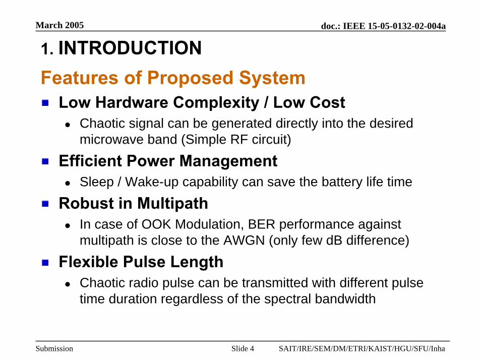
1. INTRODUCTIONFeatures of Proposed System
Low Hardware Complexity / Low CostChaotic signal can be generated directly into the desired microwave band (Simple RF circuit)
Efficient Power ManagementSleep / Wake-up capability can save the battery life time
Robust in MultipathIn case of OOK Modulation, BER performance against multipath is close to the AWGN (only few dB difference)
Flexible Pulse LengthChaotic radio pulse can be transmitted with different pulse time duration regardless of the spectral bandwidth
March 2005
Slide 5
doc.: IEEE 15-05-0132-02-004a
Submission SAIT/IRE/SEM/DM/ETRI/KAIST/HGU/SFU/Inha
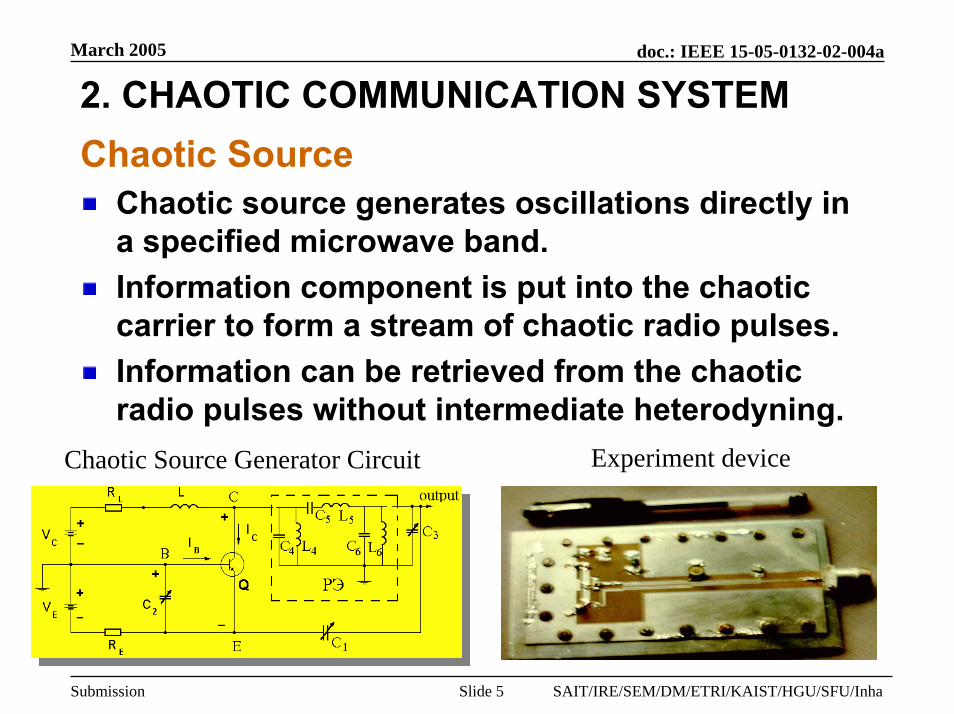
2. CHAOTIC COMMUNICATION SYSTEMChaotic Source
Chaotic source generates oscillations directly in a specified microwave band.Information component is put into the chaotic carrier to form a stream of chaotic radio pulses.Information can be retrieved from the chaotic radio pulses without intermediate heterodyning.
Experiment deviceChaotic Source Generator Circuit

March 2005
Slide 6
doc.: IEEE 15-05-0132-02-004a
Submission SAIT/IRE/SEM/DM/ETRI/KAIST/HGU/SFU/Inha
2. CHAOTIC COMMUNICATION SYSTEMSpectral Properties of Chaotic Signal
Spectral properties don’t change even though the length or duration of the chaotic pulses are varied
0 2 4 6 8 10-60
-50
-40
-30
-20
-10
0
Frequency [GHz]
Nor
mal
ized
Pow
er S
pect
ral D
ensi
ty
0 0.5 1 1.5 2 2.5 3 3.5 4
x 10-6
-5
-4
-3
-2
-1
0
1
2
3
4
Time (s)
Am
plitu
de
0 20 40 60 80 100 120 140 160 180 200-1.5
-1
-0.5
0
0.5
1
1.5
Time, t [ns]
Am
plitu
de
0 5 10 15-60
-50
-40
-30
-20
-10
0
Frequency [GHz]
Nor
malized
Pow
er S
pectra
l Den
sity Chaotic Signal
Chaotic Pulse (OOK)
March 2005
Slide 7
doc.: IEEE 15-05-0132-02-004a
Submission SAIT/IRE/SEM/DM/ETRI/KAIST/HGU/SFU/Inha
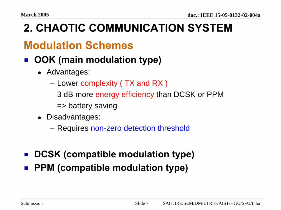
2. CHAOTIC COMMUNICATION SYSTEMModulation Schemes
OOK (main modulation type)Advantages:– Lower complexity ( TX and RX )– 3 dB more energy efficiency than DCSK or PPM
=> battery savingDisadvantages:– Requires non-zero detection threshold
DCSK (compatible modulation type)PPM (compatible modulation type)

March 2005
Slide 8
doc.: IEEE 15-05-0132-02-004a
Submission SAIT/IRE/SEM/DM/ETRI/KAIST/HGU/SFU/Inha
3.1. Unit Manufacturing Cost/ComplexityComplexity (OOK)
RF part of the transceiver:Chaotic oscillator in 3.1-5.1 GHz frequency band with 10 dBm output power amplifier (common complexity is equivalent to 4 power amplifiers) Switch-modulator LNA (amplification 30-35 dB)2 Band Pass Filter with bandwidth 1 GHz (in band 3.1-5.1 GHz)Envelope detectorAntennasNo mixers, no correlators, no RF VCO
Baseband part of the transceiver:Reference oscillator – 20 MHzBandpass amplifiersThreshold detector or 4 bit A/D converterFrequency Synthesizer on 2.002 MHz (for ranging)Digital part with ~ 10K gates
2.5125

March 2005
Slide 9
doc.: IEEE 15-05-0132-02-004a
Submission SAIT/IRE/SEM/DM/ETRI/KAIST/HGU/SFU/Inha
3.4. Technical FeasibilityPrototype 1
The communication test has successfully done using Chaotic pulses
UWB DCC-OOK Test-bed

March 2005
Slide 10
doc.: IEEE 15-05-0132-02-004a
Submission SAIT/IRE/SEM/DM/ETRI/KAIST/HGU/SFU/Inha
3.4. Technical FeasibilityPrototype 2
Battery DigitalBlock
RFReceiver
Generator
Switc
h
Ant
enna

March 2005
Slide 11
doc.: IEEE 15-05-0132-02-004a
Submission SAIT/IRE/SEM/DM/ETRI/KAIST/HGU/SFU/Inha
3.5. ScalabilityChaotic Pulse Duration
100 101 102 103 10410-7
10-6
10-5
10-4
10-3
10-2
10-1
100
2β(number of samples per one bit)
BE
R
BER with various β
Eb/No = 10dBEb/No = 12dBEb/No = 14dBEb/No = 16dBEb/No = 18dBEb/No = 20dBEb/No = 22dB
20Mbps 10Mbps 5Mbps
T Bit duration
T
T Duty Cycle
Repeated transmission
March 2005
Slide 12
doc.: IEEE 15-05-0132-02-004a
Submission SAIT/IRE/SEM/DM/ETRI/KAIST/HGU/SFU/Inha
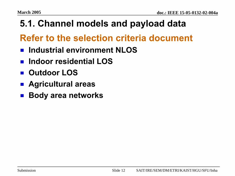
5.1. Channel models and payload dataRefer to the selection criteria document
Industrial environment NLOSIndoor residential LOSOutdoor LOSAgricultural areasBody area networks

March 2005
Slide 13
doc.: IEEE 15-05-0132-02-004a
Submission SAIT/IRE/SEM/DM/ETRI/KAIST/HGU/SFU/Inha
5.2. Size and Form FactorValues
PHY–level (130 nm technology)RF part of transceiver => 0.3 mm2
Analog part of transceiver PHY–level baseband => 0.2 mm2
Digital part of transceiver PHY–level baseband => 0.3 mm2
Common layout square for PHY-level => 1.0 mm2
Antenna: 2.0 x 2.0 cm2

March 2005
Slide 14
doc.: IEEE 15-05-0132-02-004a
Submission SAIT/IRE/SEM/DM/ETRI/KAIST/HGU/SFU/Inha
5.3. PHY-SAP Payload Bit Rate / ThroughputPayload Bit Rate
PPDU (38 Bytes)
Preamble SFD PHR PSDU
4 + 1 + 1 Bytes 32 Bytes
1 0bits
Ts
Tm
Ts = 100 ns : Pulse emission time
Tm = 400 ns : Pulse bin width or Bit period
∴ Duty cycle, D = 1/4
Ts Ts = 100 ns : Pulse emission time
Tm = 600 ns : Pulse bin width or Bit period
∴ Duty cycle, D = 1/6Tm
Nominal PHY-SAP payload bit rate, X0 = (1/400ns)×(1000/1024) = 2.44Mbps
Optional PHY-SAP payload bit rate, Xi = (1/600ns)×(1000/1024) = 1.63Mbps

March 2005
Slide 15
doc.: IEEE 15-05-0132-02-004a
Submission SAIT/IRE/SEM/DM/ETRI/KAIST/HGU/SFU/Inha
5.3. PHY-SAP Payload Bit Rate / ThroughputThroughput
Data Frame 1 (38 bytes) Data Frame 2 (38 bytes)ACK (11 bytes)
Packet 1
…32 bits 40 bits
LIFSt data-frame t ACK t ACK-frame
Time for acknowledged transmission, tpacket
tpacket = tdata-frame + t ACK + t ACK-frame + LIFS= (38×8×400ns) + (32×400ns) + (11×8×400ns) + (40×400ns)= 121.6µs + 12.8µs + 35.2µs + 16µs = 185.6µs
tpacket = tdata-frame + t ACK + t ACK-frame + LIFS= (38×8×600ns) + (32×600ns) + (11×8×600ns) + (40×600ns)= 182.4µs + 19.2µs + 52.8µs + 24µs = 278.4µs
Optional Data Throughput, Ti = (32×8/278.4µs)×(1000/1024) = 898kbpsNominal Data Throughput, T0 = (32×8/185.6µs)×(1000/1024) = 1.35Mbps

March 2005
Slide 16
doc.: IEEE 15-05-0132-02-004a
Submission SAIT/IRE/SEM/DM/ETRI/KAIST/HGU/SFU/Inha
5.4. Simultaneously Operating PiconetsThree Methods to Achieve SOP
Frequency division multiplexing (FDM)Four independent frequency channels on 500 MHz guaranties simultaneously operating four piconets.
Code division multiplexing (CDM)Deployed a class of unipolar codes (0,1) having ZCD/LCD property maintain orthogonality among piconets.Four set of codes can support four simultaneously operating piconets.
Frequency-code division multiplexing (FCDM)Two independent frequency channels with 1 GHz bandwidth and within each frequency channel, a set of codes is usedEx: Only two codes are required to support four SOPs
March 2005
Slide 17
doc.: IEEE 15-05-0132-02-004a
Submission SAIT/IRE/SEM/DM/ETRI/KAIST/HGU/SFU/Inha
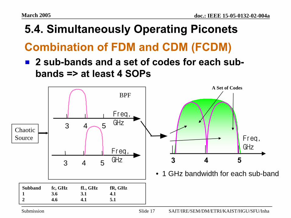
5.4. Simultaneously Operating PiconetsCombination of FDM and CDM (FCDM)
2 sub-bands and a set of codes for each sub-bands => at least 4 SOPs
3 4 5Freq,GHz
• 1 GHz bandwidth for each sub-band3 4 5
Freq,GHz 3 4 5
Freq,GHz
A Set of Codes BPF
ChaoticSource
Subband fc, GHz fL, GHz fR, GHz1 3.6 3.1 4.12 4.6 4.1 5.1

March 2005
Slide 18
doc.: IEEE 15-05-0132-02-004a
Submission SAIT/IRE/SEM/DM/ETRI/KAIST/HGU/SFU/Inha
5.4. Simultaneously Operating PiconetsCDM Methods to Achieve SOP
CDM for SOP can be achieved using UnipolarZCD/LCD Code in chaotic-OOK modulation
ZCD(Zero Correlation Duration): Local time duration with zero autocorrelation function sidelobe & zero cross-correlation function LCD(Low Correlation Duration): Local time duration with low zero autocorrelation function sidelobe & low cross-correlation function
* Local time duration function as an Interference rejection interval for SOP
Characteritics of combined schemes Simple circuit with noncoherent envelope detectorNovel Inter/Intra Piconet Interference immunity for an efficient SOP

March 2005
Slide 19
doc.: IEEE 15-05-0132-02-004a
Submission SAIT/IRE/SEM/DM/ETRI/KAIST/HGU/SFU/Inha
5.4. Simultaneously Operating PiconetsExample of Unipolar ZCD Codes Type
Type1 : Circular type sequenceA code set is constructed by chip shift of a seed code An example of (8,4,0,0) with M=2
code a=[1 0 1 0 1 0 1 0] code b=[0 1 0 1 0 1 0 1]
Type2 : Non-Circular type sequenceAn example of (5,2,0,0) with M=3
code a=[1 0 0 1 0 0] code b=[0 1 0 0 0 1] code c=[0 0 1 0 1 0]
Where (N,W,A,C) isN = sequence period, W = number of nonzero elements, A = ACF sidelobe in ZCD/LCD, C = CCF value in ZCD/LCD M = family size, Truncation of N/M = W

March 2005
Slide 20
doc.: IEEE 15-05-0132-02-004a
Submission SAIT/IRE/SEM/DM/ETRI/KAIST/HGU/SFU/Inha
5.4. Simultaneously Operating PiconetsTransceiver Architecture of Chaotic-OOKBased ZCD/LCD-CDM
t
Unipolar Code4
Tx1(Desired user)
Rx1
Spreadingt
Chaotic Source
OOK Modulation PA
RadioChannel
LNA
Received signal
BPFMatched FilterRecovered DATA
Detection
t
Tx1
Tx4
0 1 0 0 1 1 0tUnipolar DATA
1 0 0 1 0 1 0 tUnipolar DATA Spreading
t
Chaotic Source
OOK Modulation
Code1:Piconet1Code2:piconet2Code3:piconet3Code4:piconet4
CDM
t
10
PA
Unipolar Code1
0 1 0 0 1 1 0t
Envelope Detector

March 2005
Slide 21
doc.: IEEE 15-05-0132-02-004a
Submission SAIT/IRE/SEM/DM/ETRI/KAIST/HGU/SFU/Inha
5.4. Simultaneously Operating PiconetsBaseband Chaotic-OOK- ZCD-CDM

March 2005
Slide 22
doc.: IEEE 15-05-0132-02-004a
Submission SAIT/IRE/SEM/DM/ETRI/KAIST/HGU/SFU/Inha
5.4. Simultaneously Operating PiconetsChaotic-OOK-ZCD-CDM
March 2005
Slide 23
doc.: IEEE 15-05-0132-02-004a
Submission SAIT/IRE/SEM/DM/ETRI/KAIST/HGU/SFU/Inha
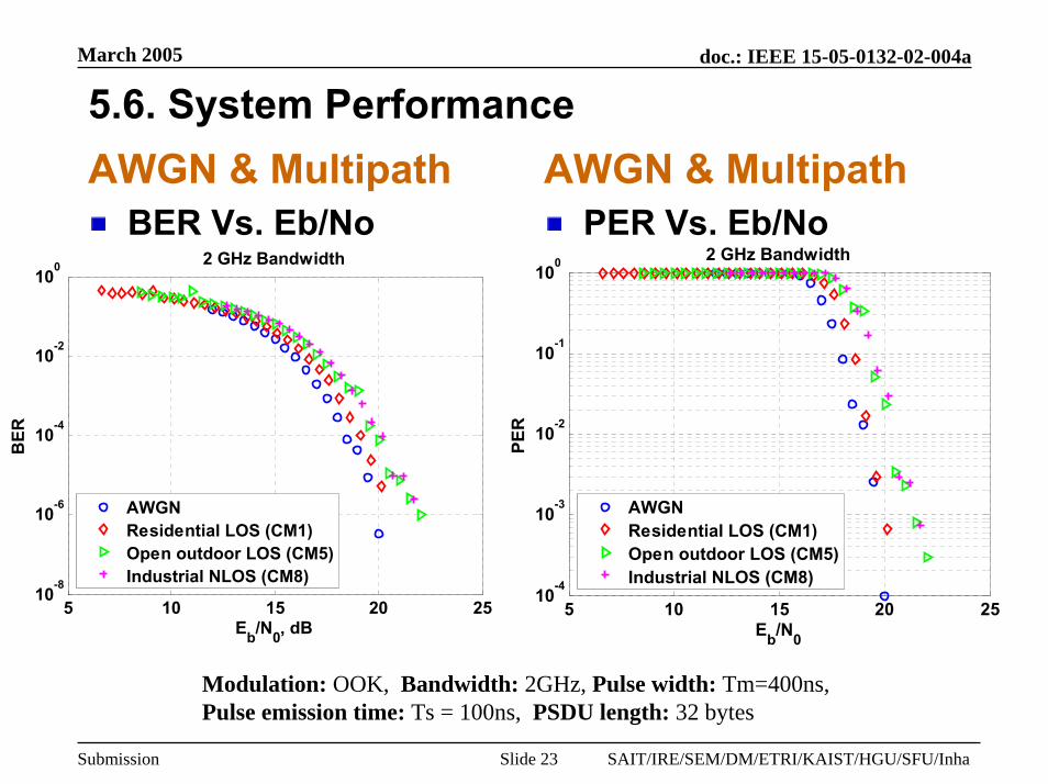
5.6. System PerformanceAWGN & Multipath
BER Vs. Eb/NoAWGN & Multipath
PER Vs. Eb/No
5 10 15 20 2510
-8
10-6
10-4
10-2
100
Eb/N0, dB
BER
2 GHz Bandwidth
AWGNResidential LOS (CM1)Open outdoor LOS (CM5)Industrial NLOS (CM8)
5 10 15 20 2510-4
10-3
10-2
10-1
100
Eb/N0
PER
2 GHz Bandwidth
AWGNResidential LOS (CM1)Open outdoor LOS (CM5)Industrial NLOS (CM8)
Modulation: OOK, Bandwidth: 2GHz, Pulse width: Tm=400ns, Pulse emission time: Ts = 100ns, PSDU length: 32 bytes
March 2005
Slide 24
doc.: IEEE 15-05-0132-02-004a
Submission SAIT/IRE/SEM/DM/ETRI/KAIST/HGU/SFU/Inha
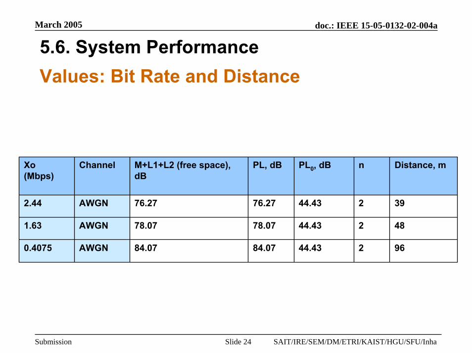
5.6. System PerformanceValues: Bit Rate and Distance
Xo(Mbps)
Channel M+L1+L2 (free space), dB
PL, dB PL0, dB n Distance, m
2.44
1.63
0.4075
AWGN 76.27 76.27 44.43 2 39
AWGN 78.07 78.07 44.43 2 48
AWGN 84.07 84.07 44.43 2 96

March 2005
Slide 25
doc.: IEEE 15-05-0132-02-004a
Submission SAIT/IRE/SEM/DM/ETRI/KAIST/HGU/SFU/Inha
5.7. RangingRanging Algorithm
yes
yes
yes
no
start both pulse sources & counter N3
no
1st delayed pulse?
start counter N1
1st overlap match?
stop N1 & N3, start N2
last overlap match?
no
stop N2, calculate Tx
•Counter N1 counts delayed pulses
•Counter N2 counts overlaps between delayed pulses(2.5000 MHz) and reference pulses(2.5125 MHz)
•Counter N3 counts reference pulses
2.5125 MHz Pulse source
2.5000 MHz Pulse source
N3 N1
Overlap detector
N2
delay
Digital Block

March 2005
Slide 26
doc.: IEEE 15-05-0132-02-004a
Submission SAIT/IRE/SEM/DM/ETRI/KAIST/HGU/SFU/Inha
5.7. Ranging
t0 t1 t2 t3
С1
С2
С3
Tx
N1
N2
N3
Tx= (N3+0.5∗N2)/f1 –(N1+0.5∗N2)/f0
distanceS = 0.5*c*(Tx-τ0)
N1, N2, N3 –pulse numbers
τ0 – retranslation time
Operation time of counters C1,C2,C3.
t**
Operation of Counters
Ref. f1
f0
March 2005
Slide 27
doc.: IEEE 15-05-0132-02-004a
Submission SAIT/IRE/SEM/DM/ETRI/KAIST/HGU/SFU/Inha
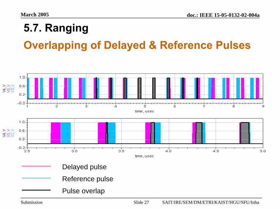
5.7. RangingOverlapping of Delayed & Reference Pulses
Delayed pulse
Reference pulse
Pulse overlap

March 2005
Slide 28
doc.: IEEE 15-05-0132-02-004a
Submission SAIT/IRE/SEM/DM/ETRI/KAIST/HGU/SFU/Inha
5.7. RangingValues: Range System supports ranges:
Range from 0 to 30 m (typical)Range up to 100 m (max 10 kbps data rate)

March 2005
Slide 29
doc.: IEEE 15-05-0132-02-004a
Submission SAIT/IRE/SEM/DM/ETRI/KAIST/HGU/SFU/Inha
5.8. Link Budget

March 2005
Slide 30
doc.: IEEE 15-05-0132-02-004a
Submission SAIT/IRE/SEM/DM/ETRI/KAIST/HGU/SFU/Inha
5.10. Power Management ModesSleep and Wake-up Scheme
Wake Up Structure
Wake Up Radio
Wake Up Signal
Main
Transceiver
Detector
Power
March 2005
Slide 31
doc.: IEEE 15-05-0132-02-004a
Submission SAIT/IRE/SEM/DM/ETRI/KAIST/HGU/SFU/Inha
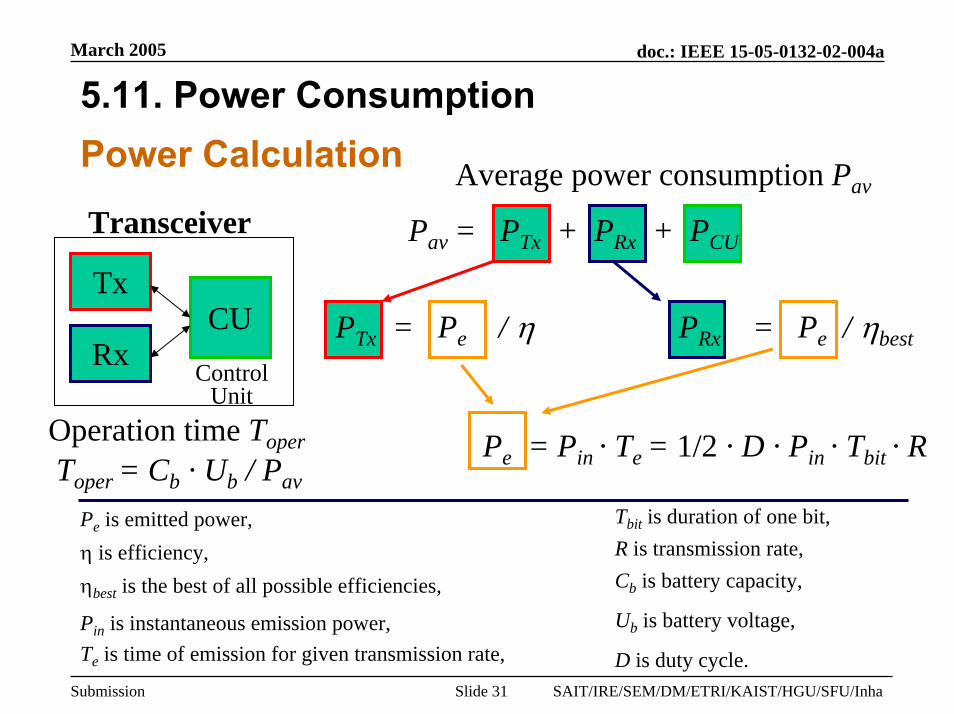
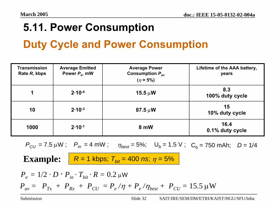
5.11. Power Consumption
Tx
RxCU
Transceiver
Pe is emitted power, η is efficiency,ηbest is the best of all possible efficiencies,
Pin is instantaneous emission power, Te is time of emission for given transmission rate,
Tbit is duration of one bit, R is transmission rate,Cb is battery capacity,
Ub is battery voltage,
D is duty cycle.
Operation time Toper
ControlUnit
Toper = Cb · Ub / Pav
Pav = PTx + PRx + PCU
PTx = Pe / η PRx = Pe / ηbest
Pe = Pin · Te = 1/2 · D · Pin · Tbit · R
Average power consumption PavPower Calculation
March 2005
Slide 32
doc.: IEEE 15-05-0132-02-004a
Submission SAIT/IRE/SEM/DM/ETRI/KAIST/HGU/SFU/Inha
5.11. Power ConsumptionDuty Cycle and Power Consumption
Transmission Rate R, kbps
Average Emitted Power Pe, mW
Average Power Consumption Pav
(η = 5%)
Lifetime of the AAA battery, years
1 2·10-4 15.5 µW 8.3100% duty cycle
10 2·10-3 87.5 µW 1510% duty cycle
1000 2·10-1 8 mW 16.40.1% duty cycle
Ub = 1.5 V ; Cb = 750 mAh; D = 1/4Pin = 4 mW ;PCU = 7.5 µW ; ηbest = 5%;
Example: R = 1 kbps; Tbit = 400 ns; η = 5%
Pe = 1/2 · D · Pin · Tbit · R = 0.2 µW
Pav = PTx + PRx + PCU = Pe /η + Pe /ηbest + PCU = 15.5 µW
March 2005
Slide 33
doc.: IEEE 15-05-0132-02-004a
Submission SAIT/IRE/SEM/DM/ETRI/KAIST/HGU/SFU/Inha
Conclusion
Chaotic communications meet the low power, low cost & low complexity requirements → best suited for 15.4a applications.Proposed DCC-OOK compliant with FCC UWB PSD regulation.Feasibility and scalability are guaranteed with precision ranging and SOP capabilities. The implemented test bed demonstrated the feasibility of DCC technology.
doc.: IEEE 15-05-0132-01-004a
Submission Slide 34 SAIT/IRE/SEM/DM/ETRI/KAIST/HGU/SFU/Inha
March 2005
DCSK: Compatible Modulation Scheme for Direct Chaotic Communication
March 2005
Slide 35
doc.: IEEE 15-05-0132-02-004a
Submission SAIT/IRE/SEM/DM/ETRI/KAIST/HGU/SFU/Inha
DCSK ModulationDCSK
Differential Chaos Shift Keying (DCSK) One of the modulation scheme as an alternative to OOKDCSK transmits a reference chaotic pulse and an information data pulse depending on whether information bit 1 (same ref. chaotic pulse) or 0 (inverted of the chaotic pulse) is being transmittedThe information signal can be recovered in the receiver by a correlator with a constant decision thresholdThe Chaotic properties are maintained as same as OOK Data rate is as same as OOKSOP can be achieved by transmitting Chaotic pulses with different length

March 2005
Slide 36
doc.: IEEE 15-05-0132-02-004a
Submission SAIT/IRE/SEM/DM/ETRI/KAIST/HGU/SFU/Inha
DCSK ModulationPrinciple
4 6 8 10 12 14 16 1810-5
10-4
10-3
10-2
10-1
100
Eb/No
BE
R
OOKDCSK
4 6 8 10 12 14 16 1810-5
10-4
10-3
10-2
10-1
100
Eb/No
BE
R
OOK Vs DCSK
Transmitter Receiver
Chaotic
Generator
Delay
T/2
-1
Data Bit Stream
Delay
T/2
Integrator
T/2T/2
TThreshold
March 2005
Slide 37
doc.: IEEE 15-05-0132-02-004a
Submission SAIT/IRE/SEM/DM/ETRI/KAIST/HGU/SFU/Inha
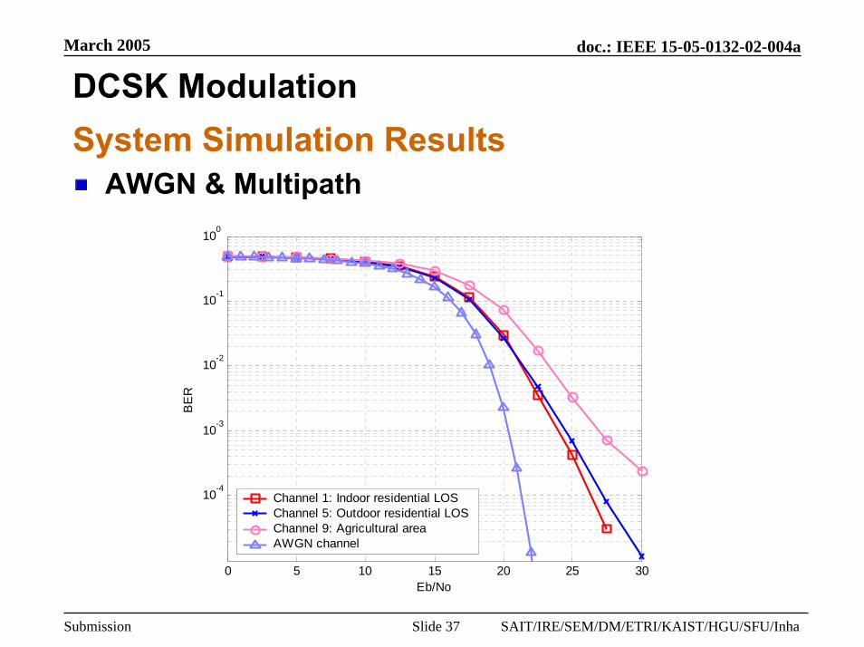
DCSK ModulationSystem Simulation Results
AWGN & Multipath
0 5 10 15 20 25 30
10-4
10-3
10-2
10-1
100
Eb/No
BE
R
Channel 1: Indoor residential LOSChannel 5: Outdoor residential LOSChannel 9: Agricultural areaAWGN channel

March 2005
Slide 38
doc.: IEEE 15-05-0132-02-004a
Submission SAIT/IRE/SEM/DM/ETRI/KAIST/HGU/SFU/Inha
DCSK Modulation
0 1000 2000 3000 4000 5000 6000-5
0
5Piconet1
0 1000 2000 3000 4000 5000 6000-5
0
5Piconet2
0 1000 2000 3000 4000 5000 6000-5
0
5Piconet3
0 1000 2000 3000 4000 5000 6000-5
0
5Piconet4
0 1000 2000 3000 4000 5000 6000-10
0
10All
Piconet 1 Piconet 1
Piconet 1 User Piconet 1 User
Detection Detection
Piconet 2 Piconet 2
Piconet 3 Piconet 3
Piconet 4 Piconet 4
-20 -18 -16 -14 -12 -10 -8 -6 -4 -2 010-3
10-2
10-1
100
S/N
BE
R
4 Users
8Mbps5Mbps
SOP: LDMA•In DCSK SOP can be done using Chaotic Length Division Multiple Access (LDMA)
•LDMA works based on the exploitation of different chaotic length assigned to each piconets.
•LDMA is based on the spectral and correlation property of chaotic signal
March 2005
Slide 39
doc.: IEEE 15-05-0132-02-004a
Submission SAIT/IRE/SEM/DM/ETRI/KAIST/HGU/SFU/Inha
DCSK Modulation
Chaotic Gain in DCSK
-20 -19 -18 -17 -16 -15 -14 -13 -12 -11 -1010
-3
10-2
10-1
100
S/N
BE
R
Gain
5Mbps4Mbps2Mbps0 1 0 0 0 2 0 0 0 3 0 0 0 4 0 0 0 5 0 0 0 6 0 0 0 7 0 0 0 8 0 0 0 9 0 0 0 1 0 0 0 0
- 5
0
5
0 1 0 0 0 2 0 0 0 3 0 0 0 4 0 0 0 5 0 0 0 6 0 0 0 7 0 0 0 8 0 0 0 9 0 0 0 1 0 0 0 0- 5
0
5
0 1 0 0 0 2 0 0 0 3 0 0 0 4 0 0 0 5 0 0 0 6 0 0 0 7 0 0 0 8 0 0 0 9 0 0 0 1 0 0 0 0- 5
0
5
Bit = 1 0
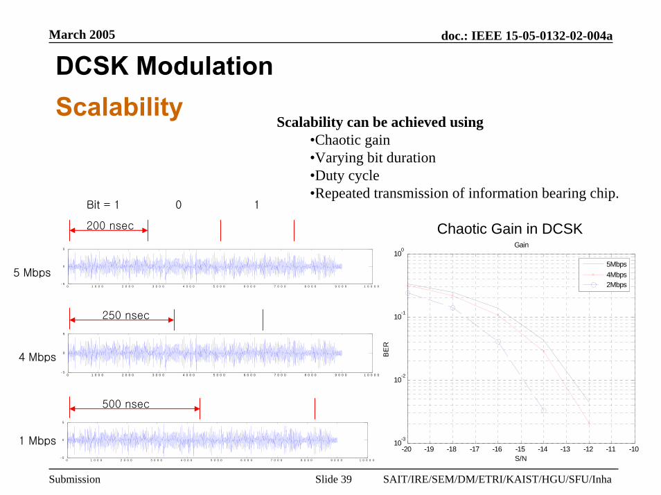
200 nsec
250 nsec
500 nsec
5 Mbps
4 Mbps
1 Mbps
1
Scalability can be achieved using•Chaotic gain•Varying bit duration•Duty cycle•Repeated transmission of information bearing chip.
Scalability
March 2005
Slide 40
doc.: IEEE 15-05-0132-02-004a
Submission SAIT/IRE/SEM/DM/ETRI/KAIST/HGU/SFU/Inha
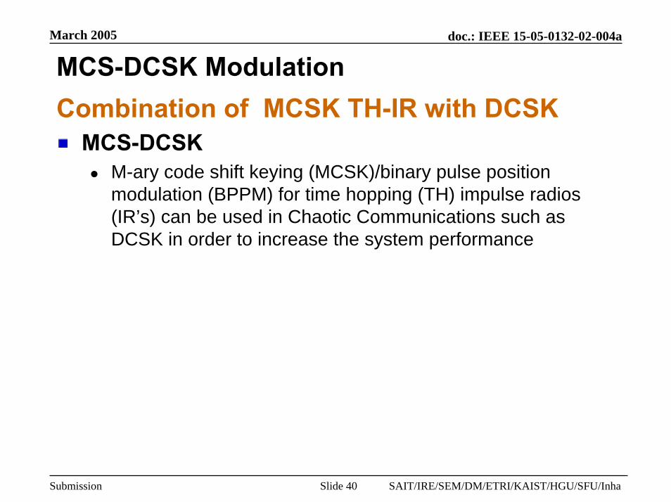
MCS-DCSK ModulationCombination of MCSK TH-IR with DCSK
MCS-DCSK M-ary code shift keying (MCSK)/binary pulse position modulation (BPPM) for time hopping (TH) impulse radios (IR’s) can be used in Chaotic Communications such as DCSK in order to increase the system performance

March 2005
Slide 41
doc.: IEEE 15-05-0132-02-004a
Submission SAIT/IRE/SEM/DM/ETRI/KAIST/HGU/SFU/Inha
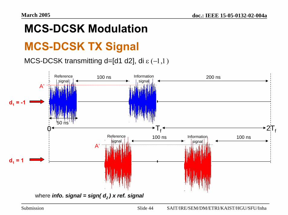
MCS-DCSK ModulationDCSK TX Signal
DCSK transmitting d=[d1 d2], di ε (−1,1)
50 ns
50 ns
d1 (bit-1)transmitted
d2 (bit-2)transmitted
Referencesignal
Informationsignal 50 ns
Referencesignal
Informationsignal
50 ns 50 ns
where info. signal = sign( di ) x ref. signal
0 Tf 2Tf
A
March 2005
Slide 42
doc.: IEEE 15-05-0132-02-004a
Submission SAIT/IRE/SEM/DM/ETRI/KAIST/HGU/SFU/Inha
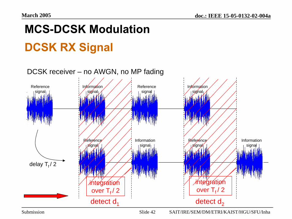
MCS-DCSK ModulationDCSK RX Signal
DCSK receiver – no AWGN, no MP fading
Referencesignal
Informationsignal
Referencesignal
Referencesignal
Informationsignal
Informationsignal
delay Tf / 2
integration over Tf / 2
Informationsignal
Referencesignal
integration over Tf / 2
detect d1 detect d2

March 2005
Slide 43
doc.: IEEE 15-05-0132-02-004a
Submission SAIT/IRE/SEM/DM/ETRI/KAIST/HGU/SFU/Inha
MCS-DCSK Modulation
DCSK: Transmitted and received signals (CM1, no AWGN)DCSK TX and RX Signal
March 2005
Slide 44
doc.: IEEE 15-05-0132-02-004a
Submission SAIT/IRE/SEM/DM/ETRI/KAIST/HGU/SFU/Inha
MCS-DCSK ModulationMCS-DCSK TX SignalMCS-DCSK transmitting d=[d1 d2], di ε (−1,1)
50 ns
100 nsReferencesignal
Informationsignal
where info. signal = sign( d2 ) x ref. signal
0 Tf 2Tf100 ns 100 ns
200 ns
d1 = -1
d1 = 1
A’
A’
Informationsignal
Referencesignal

March 2005
Slide 45
doc.: IEEE 15-05-0132-02-004a
Submission SAIT/IRE/SEM/DM/ETRI/KAIST/HGU/SFU/Inha
MCS-DCSK ModulationMCS-DCSK RX Signal
Referencesignal
Informationsignal
Referencesignal
)1(d̂1 − )1(d̂1
2Tf
Informationsignal
Referencesignal
delay 3Tf / 4
integrate over Tf / 2
0
integrate over Tf / 2
1d)1(d̂)1(d̂ -1;d)1(d̂)1(d̂ 111111 =⎯ →⎯<−=⎯ →⎯>−
( ) ( )(1)d̂signd 1d if ; (-1)d̂signd -1d if 121121 =⎯ →⎯==⎯ →⎯=Decision
Step 1:
Step 2:
MCS-DCSK receiver – no AWGN, no MP fading
Referencesignal

March 2005
Slide 46
doc.: IEEE 15-05-0132-02-004a
Submission SAIT/IRE/SEM/DM/ETRI/KAIST/HGU/SFU/Inha
MCS-DCSK ModulationMCS-DCSK TX and RX Signal
MCS-DCSK: Transmitted and received signals (CM1, no AWGN)

March 2005
Slide 47
doc.: IEEE 15-05-0132-02-004a
Submission SAIT/IRE/SEM/DM/ETRI/KAIST/HGU/SFU/Inha
MCS-DCSK ModulationMCS-DCSK Simulation Results
4 6 8 10 12 14 1610-6
10-5
10-4
10-3
10-2
10-1
100
Eb/N0 (dB)
BE
R
Channel: AWGN
DCSK - 2.0GHz BWMCS-DCSK - 2.0GHz BWDCSK - 1.0GHz BWMCS-DCSK - 1.0GHz BWDCSK - 0.5GHz BWMCS-DCSK - 0.5GHz BW

March 2005
Slide 48
doc.: IEEE 15-05-0132-02-004a
Submission SAIT/IRE/SEM/DM/ETRI/KAIST/HGU/SFU/Inha
MCS-DCSK ModulationMCS-DCSK Simulation Results
4 6 8 10 12 14 1610-4
10-3
10-2
10-1
100
Eb/N0 (dB)
BE
R
Channel: Residential LOS
DCSK - 0.5GHz BWDCSK - 1.0GHz BWDCSK - 2.0GHz BWMCS-DCSK - 0.5GHz BWMCS-DCSK - 1.0GHz BWMCS-DCSK - 2.0GHz BW

March 2005
Slide 49
doc.: IEEE 15-05-0132-02-004a
Submission SAIT/IRE/SEM/DM/ETRI/KAIST/HGU/SFU/Inha
DCSK ModulationComplexity, Cost & Technical Feasibility
Complexity and cost will be slightly higher compare to the OOK chaotic system proposed
ConclusionChaotic communication based on DCSK modulation is an alternative solution for TG4a.Most hardware from OOK is retained.SOP and ranging can be solved effectively using DCSK.

doc.: IEEE 15-05-0132-01-004a
Submission Slide 50 SAIT/IRE/SEM/DM/ETRI/KAIST/HGU/SFU/Inha
March 2005
MC-PPM : Compatible Modulation Scheme for Direct Chaotic Communication

March 2005
Slide 51
doc.: IEEE 15-05-0132-02-004a
Submission SAIT/IRE/SEM/DM/ETRI/KAIST/HGU/SFU/Inha
MC-PPM ModulationMC-PPM
Multi-coded Pulse Position Modulation (MC-PPM) Power efficient schemeInherent coding gain due to orthogonal multi-codes Support wide pulse shaping in same data rate conditionConstant decision threshold in the receiverOOK is one special mode of MC-PPM

March 2005
Slide 52
doc.: IEEE 15-05-0132-02-004a
Submission SAIT/IRE/SEM/DM/ETRI/KAIST/HGU/SFU/Inha
MC-PPM ModulationPrinciple
Principle operation (L=3, Ns=4)
Modulation
Data block( L bits )Ex. L=3
Orthogonal code set( Code Length : Ns )
Ex. Ns=4
Multi-coded symbol( Code rate : L/Ns )Ex. Code rate = 3/4
1
-1
1
1-1-11
-1-111
-11-11
1-1-11
11-1-1
-11-11
⊕⊗⊗⊗
===
11-31=
MC-PPM Signal :
1 -3 1 1

March 2005
Slide 53
doc.: IEEE 15-05-0132-02-004a
Submission SAIT/IRE/SEM/DM/ETRI/KAIST/HGU/SFU/Inha
MC-PPM ModulationData Frame Structure
1 data block (L data) interval of PSDU :
1 2 rN
sN
: # of Repetitions
: Orthogonal Code length
sT
cT1L +
1 2 sN
12 1L + : Position number for MC-PPM
mT
rN
gT gT gT
dT
...
...
...
Preamble SFD PHR PSDU
s
r
m
c
s
g
d
LNNTTTT
T
: # of bits per data block
: Orthogonal code length
: # of repetitions
: Pulse bin width (duration)
: Total transmit time duration of a data block
: Guard time for processing delay
: Multi-coded chip duration
: Multi-coded symbol duration
4 1 1 32
( ), , ( 1)d r s g s s c c mT N T T T N T T L T= + = = +
March 2005
Slide 54
doc.: IEEE 15-05-0132-02-004a
Submission SAIT/IRE/SEM/DM/ETRI/KAIST/HGU/SFU/Inha
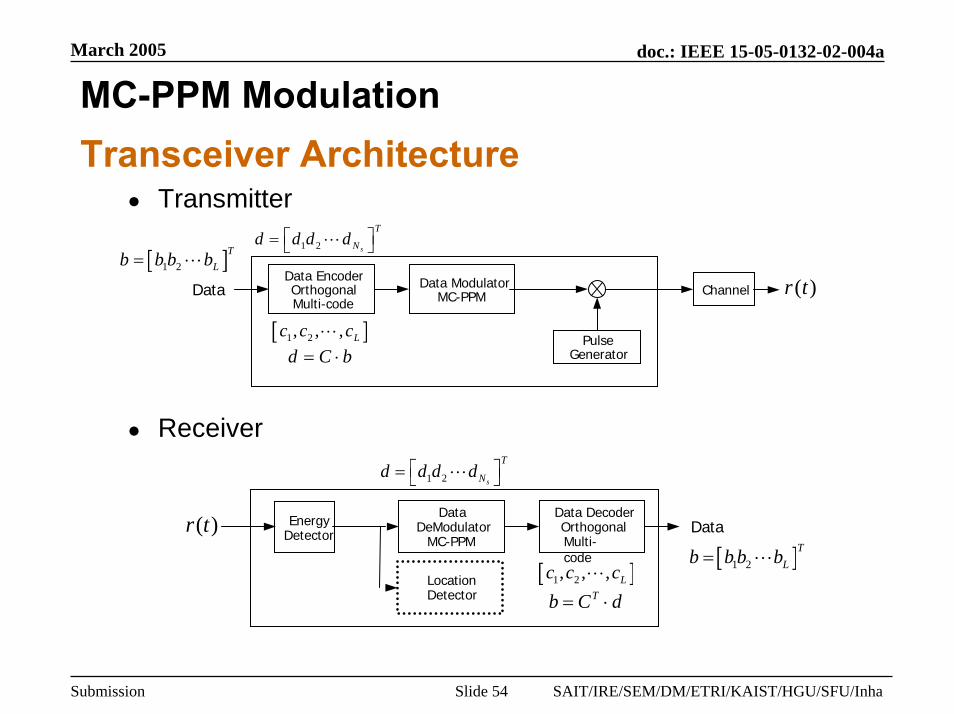
MC-PPM ModulationTransceiver Architecture
Transmitter
Receiver
[ ]1 2T
Lb b b b= L1 2 s
T
Nd d d d⎡ ⎤= ⎣ ⎦L
[ ]1 2, , , Lc c cL
d C b= ⋅
( )r tData ModulatorMC-PPM Channel
Data EncoderOrthogonalMulti-code
Data
PulseGenerator
[ ]1 2T
Lb b b b= L[ ]1 2, , , Lc c cL
Tb C d= ⋅
1 2 s
T
Nd d d d⎡ ⎤= ⎣ ⎦L
( )r tData DecoderOrthogonalMulti-code
DataDeModulator
MC-PPMDataEnergy
Detector
LocationDetector

March 2005
Slide 55
doc.: IEEE 15-05-0132-02-004a
Submission SAIT/IRE/SEM/DM/ETRI/KAIST/HGU/SFU/Inha
MC-PPM ModulationPHY-SAP Data Rates
Flexible data rates can be supported according to several designparameter (Tm, L, Ns, Nr, Tg)
20pT ns=
200mT ns=
Tp Tm L Ns Nr TgDataRate
20ns 200ns
200ns
200ns
1 16 128
200ns
1.190 kbps
20ns 3 16 1
0ns
0ns
0ns
228 kbps
20ns 3 8 1 457 kbps
20ns 0ns1 1 1 2.44 Mbps

March 2005
Slide 56
doc.: IEEE 15-05-0132-02-004a
Submission SAIT/IRE/SEM/DM/ETRI/KAIST/HGU/SFU/Inha
MC-PPM ModulationData Throughput
Data Throughput
Transmission time (ttx) & Data throughput (Rth)For L=3, Ns=8, Nr=1,Tg=0ns (457kbps)– ttx = tlong_frame + tACK + tACK_frame + LIFS
= 614.4 u + 25.6 u + 187.7 u + 85.3 u = 913 u– Rth = 32×8 / 913u ≈ 280.3 kbps
( Nominal throughput based on 32 bytes payload )For L=3, Ns=16, Nr=1,Tg=0ns (228kbps)– ttx = tlong_frame + tACK + tACK_frame + LIFS
= 1228.8 u + 51.2 u + 375.5 u + 170.7 u = 1826.2 u– Rth = 32×8 / 1826.2 u ≈ 140.2 kbps
( Nominal throughput based on 32 bytes payload )
LIFStACKtlong_frame tACK_frame
∙∙∙∙ ∙∙∙∙ ∙∙∙∙
ttx

March 2005
Slide 57
doc.: IEEE 15-05-0132-02-004a
Submission SAIT/IRE/SEM/DM/ETRI/KAIST/HGU/SFU/Inha
MC-PPM ModulationSignal Acquisition
Energy detection based acquisitionAcquisition should be performed in order to make synchronization and demodulate dataSynchronization : Non-coherent
March 2005
Slide 58
doc.: IEEE 15-05-0132-02-004a
Submission SAIT/IRE/SEM/DM/ETRI/KAIST/HGU/SFU/Inha
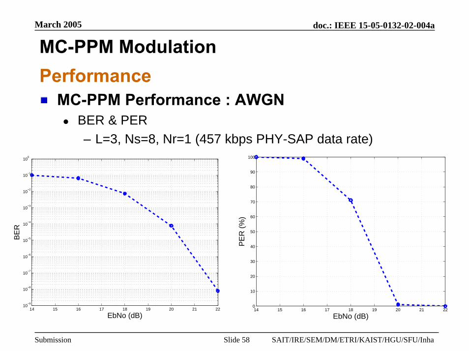
MC-PPM ModulationPerformance
MC-PPM Performance : AWGNBER & PER– L=3, Ns=8, Nr=1 (457 kbps PHY-SAP data rate)
14 15 16 17 18 19 20 21 220
10
20
30
40
50
60
70
80
90
100
EbNo (dB)
PE
R (
%)
14 15 16 17 18 19 20 21 2210
−9
10−8
10−7
10−6
10−5
10−4
10−3
10−2
10−1
100
EbNo (dB)
BE
R

March 2005
Slide 59
doc.: IEEE 15-05-0132-02-004a
Submission SAIT/IRE/SEM/DM/ETRI/KAIST/HGU/SFU/Inha
MC-PPM ModulationPerformance
MC-PPM Performance : 4a Channel ModelsBER & PER– L=3, Ns=8, Nr=1
22 23 24 25 26 27 2810
−9
10−8
10−7
10−6
10−5
10−4
10−3
10−2
10−1
100
EbNo (dB)
BE
R
CM8CM1CM5
22 23 24 25 26 27 280
10
20
30
40
50
60
70
80
90
100
EbNo (dB)
PE
R
CM8CM1CM5

March 2005
Slide 60
doc.: IEEE 15-05-0132-02-004a
Submission SAIT/IRE/SEM/DM/ETRI/KAIST/HGU/SFU/Inha
MC-PPM ModulationSOPs
Time DivisionConfiguration of SOPs– Self configuration of SOPs is possible
Piconet #1
Active Inactive
Piconet #2
Piconet #3
March 2005
Slide 61
doc.: IEEE 15-05-0132-02-004a
Submission SAIT/IRE/SEM/DM/ETRI/KAIST/HGU/SFU/Inha
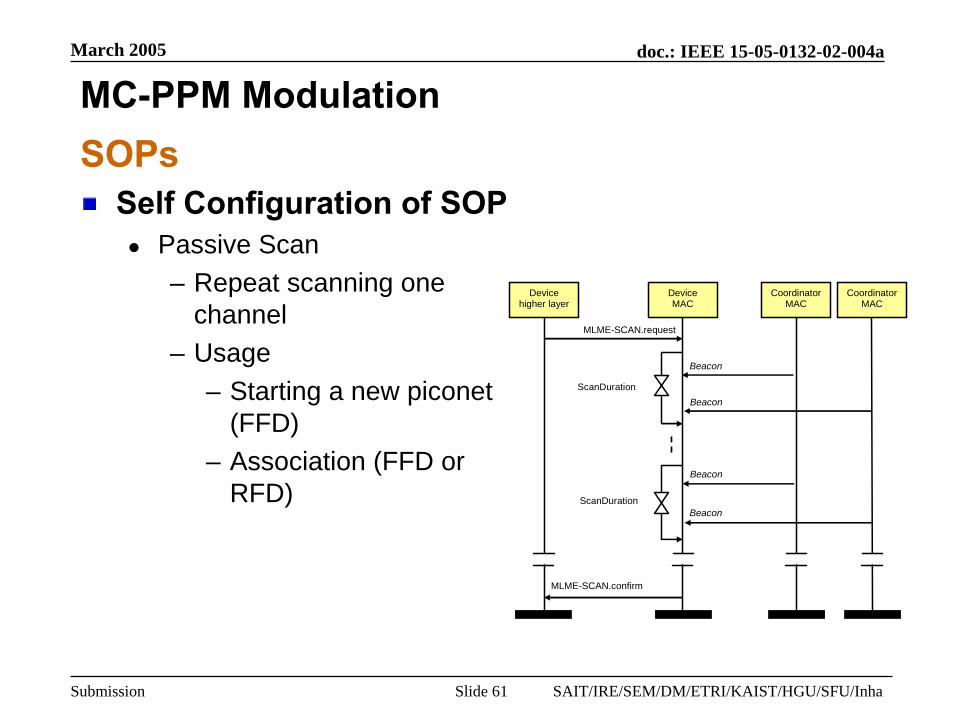
MC-PPM ModulationSOPs
Self Configuration of SOPPassive Scan– Repeat scanning one
channel– Usage
– Starting a new piconet (FFD)
– Association (FFD or RFD)
Device MAC
Coordinator MAC
Device higher layer
MLME-SCAN.request
MLME-SCAN.confirm
ScanDuration
Beacon
Coordinator MAC
Beacon
ScanDuration
Beacon
Beacon
March 2005
Slide 62
doc.: IEEE 15-05-0132-02-004a
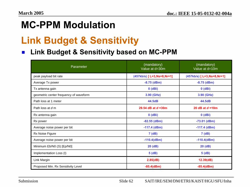
Submission SAIT/IRE/SEM/DM/ETRI/KAIST/HGU/SFU/Inha
MC-PPM ModulationLink Budget & Sensitivity
Link Budget & Sensitivity based on MC-PPM
Parameter (mandatory)Value at d=30m
(mandatory)Value at d=10m
peak payload bit rate (457kb/s) [ L=3,Ns=8,Nr=1] (457kb/s) [ L=3,Ns=8,Nr=1]
Average Tx power -8.75 (dBm) -8.75 (dBm)
Tx antenna gain 0 (dBi) 0 (dBi)
geometric center frequency of waveform 3.90 (GHz) 3.90 (GHz)
Path loss at 1 meter 44.5dB 44.5dB
Path loss at d m 29.54 dB at d =30m 20 dB at d =10m
Rx antenna gain 0 (dBi) 0 (dBi)
Rx power -82.55 (dBm) -73.01 (dBm)
Average noise power per bit -117.4 (dBm) -117.4 (dBm)
Rx Noise Figure 7 (dB) 7 (dB)
Average noise power per bit -110.4(dBm) -110.4(dBm)
Minimum Eb/N0 (S) [Ep/N0] 20 (dB) 20 (dB)
Implementation Loss (I) 5 (dB) 5 (dB)
Link Margin 2.85(dB) 12.39(dB)
Proposed Min. Rx Sensitivity Level -85.4(dBm) -85.4(dBm)
March 2005
Slide 63
doc.: IEEE 15-05-0132-02-004a
Submission SAIT/IRE/SEM/DM/ETRI/KAIST/HGU/SFU/Inha
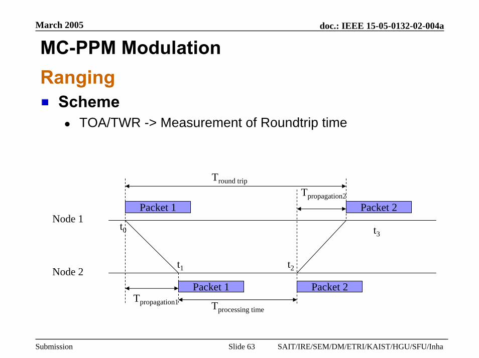
MC-PPM ModulationRanging
SchemeTOA/TWR -> Measurement of Roundtrip time
Packet 1Node 1
Node 2t1
t0
t2
t3
Tprocessing time
Tpropagation2
Packet 2
Packet 1 Packet 2Tpropagation1
Tround trip

March 2005
Slide 64
doc.: IEEE 15-05-0132-02-004a
Submission SAIT/IRE/SEM/DM/ETRI/KAIST/HGU/SFU/Inha
MC-PPM ModulationRanging
Performance
• 802.15.4a channel (cm4)• Single user• No narrowband
interference• Pulse width = 20ns• Integration time = 2ns• Pulse repetition period =
200ns• Length of search region =
40ns• Threshold level was
determined relative to noise floor
• A separate envelope detector for range estimation was employed

doc.: IEEE 15-05-0132-01-004a
Submission Slide 65 SAIT/IRE/SEM/DM/ETRI/KAIST/HGU/SFU/Inha
March 2005
Backup Slides

March 2005
Slide 66
doc.: IEEE 15-05-0132-02-004a
Submission SAIT/IRE/SEM/DM/ETRI/KAIST/HGU/SFU/Inha
Tolerance of Components
Capacitor, C1 and inductance, L → 20% tolerance.C2 and resistors, RE and R1 → 5% tolerance.
E
C
Vampin Vampout VoutRR12R=50 Ohmv a_hp_MGA-66100_19930601
Amp1
CC20C=100 pF
DA_LCBandpassDT1_colp_collector_amp_f ltDA_LCBandpassDT1
Rl=50 OhmRg=50 OhmResponseTy pe=EllipticN=4As=40 dBAp=3 dBFs2=6 GHzFp2=5.1 GHzFp1=3.1 GHzFs1=2 GHz
DT
CC16C=C2 R
RE1R=RE
V_DCSRC2Vdc=VE
V_DCSRC1Vdc=VC
RRL1R=RL
LL10L=L
BFP620X3
CC17C=C1

March 2005
Slide 67
doc.: IEEE 15-05-0132-02-004a
Submission SAIT/IRE/SEM/DM/ETRI/KAIST/HGU/SFU/Inha
Summary of Features
Information carrier Chaotic radio pulses
Band division3 bands within FCC Mask
(3.1-5.1, 6.1-8.1 and 8.2-10.2 GHz)
Channel bandwidth 2.0 GHz band or 4 channels with 500 MHz in each in the 2 GHz band
Pulse duration 400 ns
Individual bit rate 1 Kbps 10 Kbps 100 Kbps
Transmit power -30 dBm -20 dBm -20 dBm
Battery life
2.5 year100% duty
cycle
2.5 year10% duty
cycle
2.5 year0.1% duty
cycle
Aggregated bit rate Up to 5 Mbps

March 2005
Slide 68
doc.: IEEE 15-05-0132-02-004a
Submission SAIT/IRE/SEM/DM/ETRI/KAIST/HGU/SFU/Inha
Tiny Chaotic Transmitter
Transmitter consists of:- chaos generator
- modulator- antenna
Frequency band - 2-4 GHzRadiating power - 3-4 mw
March 2005
Slide 69
doc.: IEEE 15-05-0132-02-004a
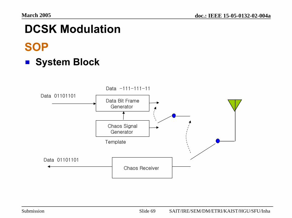
Submission SAIT/IRE/SEM/DM/ETRI/KAIST/HGU/SFU/Inha
DCSK Modulation SOP
System Block
Data Bit FrameGenerator
Chaos SignalGenerator
Data 01101101
Data -111-111-11
Template
Chaos Receiver
Data 01101101

March 2005
Slide 70
doc.: IEEE 15-05-0132-02-004a
Submission SAIT/IRE/SEM/DM/ETRI/KAIST/HGU/SFU/Inha
DCSK ModulationSOP
Transmission
T1 D1nD11 T2 D2nD21T1 D1nD11 T2 D2nD21
D11 D2nD21D1nT1 T2
Frame1
Frame2
Piconet1
Piconet2
Template Bit
Bit Frame

March 2005
Slide 71
doc.: IEEE 15-05-0132-02-004a
Submission SAIT/IRE/SEM/DM/ETRI/KAIST/HGU/SFU/Inha
DCSK ModulationSOP
DetailIntegrator
∫Data
Template
1 1 0 ………. 0
Z
Z
Z
Z
1 bit Duration
Receiver Details
March 2005
Slide 72
doc.: IEEE 15-05-0132-02-004a
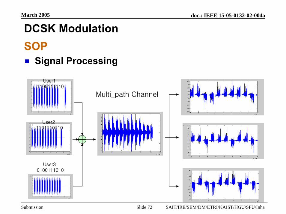
Submission SAIT/IRE/SEM/DM/ETRI/KAIST/HGU/SFU/Inha
DCSK ModulationSOP
Signal Processing
User11100111110
User21101110110
Multi_path Channel
User30100111010

March 2005
Slide 73
doc.: IEEE 15-05-0132-02-004a
Submission SAIT/IRE/SEM/DM/ETRI/KAIST/HGU/SFU/Inha
DCSK ModulationRanging
Block Diagram
Envelop Detection&
Signal Point DetectionZ-1 Serial-to-Parallel
Delay Circuit

March 2005
Slide 74
doc.: IEEE 15-05-0132-02-004a
Submission SAIT/IRE/SEM/DM/ETRI/KAIST/HGU/SFU/Inha
DCSK ModulationRanging
DeviceCoordinator
Source Time Counter+ Target Time Counter
Source Time Counter
Source Time Counter+ Target Time Counter1. Offset by Comparison
between (Source Time Counter -Target Time Counter) & (Source Time Counter - Source2 Time Counter)
2. Distance from (Source Time Counter - Source2 Time Counter)
- Offset
Adjusting Time CounterBy Offset
+ Offset
Confirm CounterJustification
0
Completion

March 2005
Slide 75
doc.: IEEE 15-05-0132-02-004a
Submission SAIT/IRE/SEM/DM/ETRI/KAIST/HGU/SFU/Inha
DCSK ModulationRanging
Coordinator Device (-2 Offset)
Initial : 356 358 1st Pass : 364 356+8 374 358+16
1. PNC recalculates Device Arrival time : 366 358 + (16/2)2. Compare value from 1 and Device : -2 364 – 3663. +2 Transferred as –Offset4. 8 Kept for Distance between PNC and Device

March 2005
Slide 76
doc.: IEEE 15-05-0132-02-004a
Submission SAIT/IRE/SEM/DM/ETRI/KAIST/HGU/SFU/Inha
DCSK ModulationLocation Awareness Special Mode
Timing Counter Fine SynchronizationPNC disseminates special frame to inform Device of Location special modeDevice acknowledges with its own timing countPNC compares its own count with Device’s count, and extract an offset between themPNC sends negative offset in order for Device to compensate its timerDevice informs PNC of all being set

March 2005
Slide 77
doc.: IEEE 15-05-0132-02-004a
Submission SAIT/IRE/SEM/DM/ETRI/KAIST/HGU/SFU/Inha
DCSK ModulationLocation Awareness Special Mode
∇ X
∇ Y
Template Frame Data Frame
Data
Template
Envelop Detection
Delay Circuit by 1~3 ns

March 2005
Slide 78
doc.: IEEE 15-05-0132-02-004a
Submission SAIT/IRE/SEM/DM/ETRI/KAIST/HGU/SFU/Inha
DCSK ModulationRanging
Fine Precision TOA EstimationSuggest Special mode different from Normal mode, which needs faster clockIn special mode, Estimate how far Signal detached from fixed time slot with finer clockThis obtained value returned with Responsecommand to Request command from MAC
March 2005
Slide 79
doc.: IEEE 15-05-0132-02-004a
Submission SAIT/IRE/SEM/DM/ETRI/KAIST/HGU/SFU/Inha
DCSK ModulationRanging
Delay Circuit
Phase 0
Phase 90
Phase 180
Phase 270
100 MHz
2.5 ns
March 2005
Slide 80
doc.: IEEE 15-05-0132-02-004a
Submission SAIT/IRE/SEM/DM/ETRI/KAIST/HGU/SFU/Inha
DCSK ModulationRanging
Simulation (BNR 16dB)
real distance : 0.968 meter2.5 ns precision distance : 0.750 meterError : -0.218 meter
Maximum Index of Moving
Average by duty cycleDuration will be convertedto distance.
real distance : 13.118 meter2.5 ns precision distance : 12.750 meterError : -0.367 meter