Embed Size (px)
Citation preview

1
Dislocations in SiGe planar waveguides
Andrea Trita
Laboratory of Quantum Electronics and Nonlinear OpticsElectronics Department - University of Pavia

2
OUTLINEIntroduction
Dislocations in SiGe planar waveguides:Consequences on the guided optical field
Silicon photonicsThe SiGe/Si approach to Silicon PhotonicsDislocations formation at SiGe/Si interfaces

3
OUTLINEIntroduction
Dislocations in SiGe planar waveguides:Consequences on the guided optical field
Silicon photonicsThe SiGe/Si approach to Silicon PhotonicsDislocations formation at SiGe/Si interfaces

4
Opticalinterconnects
Silicon Photonics
Cheap photonic chips foroptical communications industry
5
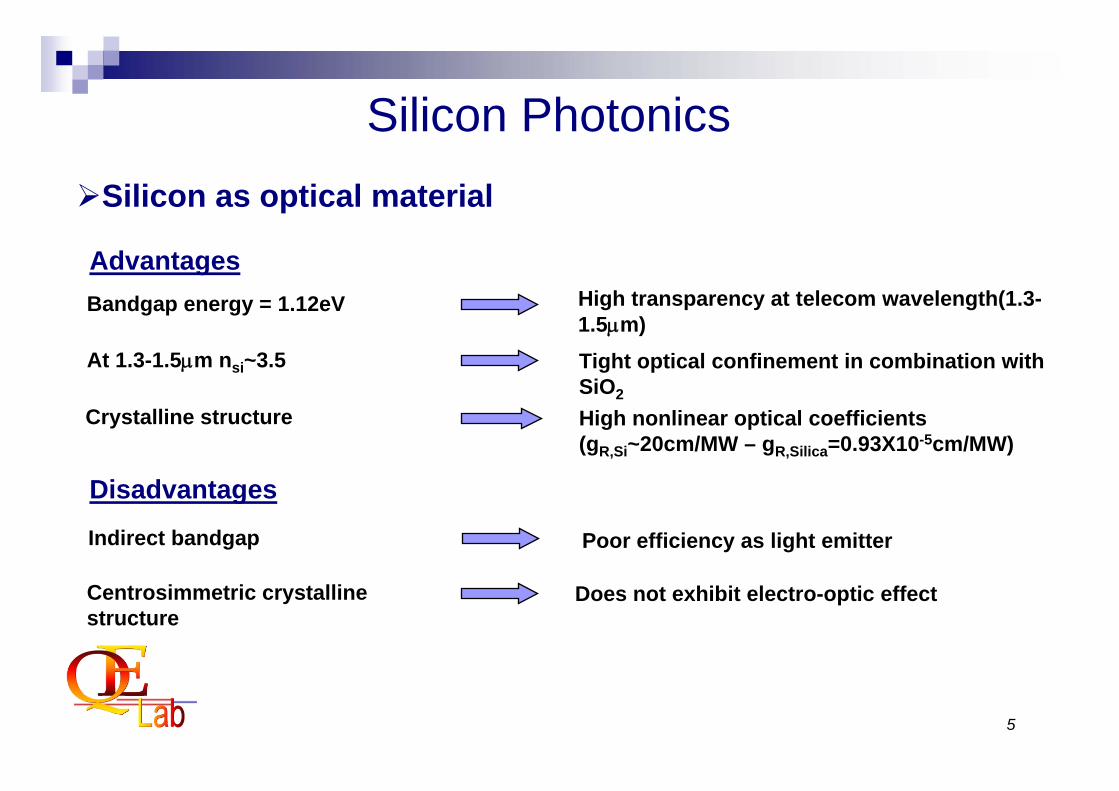
Silicon PhotonicsSilicon as optical material
Indirect bandgap Poor efficiency as light emitter
Centrosimmetric crystallinestructure
Does not exhibit electro-optic effect
Disadvantages
Bandgap energy = 1.12eV High transparency at telecom wavelength(1.3-1.5μm)
At 1.3-1.5μm nsi~3.5 Tight optical confinement in combination withSiO2
Crystalline structure High nonlinear optical coefficients(gR,Si~20cm/MW – gR,Silica=0.93X10⁻⁵cm/MW)
Advantages

6
Silicon PhotonicsThe optical waveguide.
Cladding (n1)
Core (n2)
n2>n1

7
Silicon PhotonicsThe optical waveguide.
n2>n1

8
Silicon PhotonicsTechnological approaches
SOI approachSi
SiO2
SiO. Boyraz and B. Jalali, "Demonstration of a silicon Raman laser," Opt. Express 12, 5269-5273 (2004)
SiGe/Si approachSi
SiGe
Si
SiGeSi
Possibility to tune the optical properties of the material acting on the Gefraction
At low Ge fraction the small index contrast between Si and SiGe allows formonomodal structures with micrometric dimensions
Elevated nonlinear optical coefficients
9
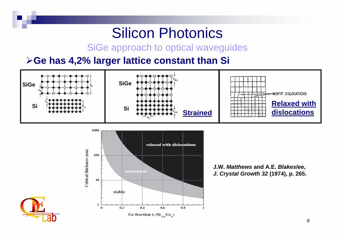
J.W. Matthews and A.E. Blakeslee, J. Crystal Growth 32 (1974), p. 265.
Ge has 4,2% larger lattice constant than Si
Si
SiGe
Si
SiGe
StrainedRelaxed withdislocations
Silicon PhotonicsSiGe approach to optical waveguides

10
OUTLINEIntroduction
Dislocations in SiGe planar waveguides:Consequences on the guided optical field
Silicon photonicsThe SiGe/Si approach to Silicon PhotonicsDislocations formation at SiGe/Si interfaces

11
PRIN Project 2005: “SiGe optical waveguides: design, fabrication, characterisation and their application to Raman amplication”
Laboratory of Quantum Electronics and Nonlinear Optics- University of Pavia
L-NESS (Laboratory for Epitaxial Nanostructures on Silicon and Spintronics) – Politecnico di Milano
Material Science Department - University of Milano BicoccaPhysics Department -University of Insubria
Dislocations in SiGe planar waveguides

12
Si capSi1-xGex layer
Si Substrate
d
Dislocations in SiGe planar waveguides
6102#75425102#7544
4102#7546
2102#7382
2101.5#76892100.8#76932100.4#7646
2100.2#7645
Nominalx
SiGe cap
[μm]SiGe layer
d [μm]Samplenumber
Fixedd
varyingx
Fixedx
varyingd

13
Dislocations in SiGe planar waveguidesConsequences on the guided optical field
1.55 μm LASER
SOURCE
Si capSi1-xGex layer
Si Substrate
VIDICON CAMERA
Cylindricallens
40X objective
Collimator
xz
y
6102#75425102#7544
4102#7546
2102#7382
2101.5#76892100.8#76932100.4#7646
2100.2#7645
Nominalx
SiGe cap
[μm]SiGe layer
d [μm]Samplenumber
Fixedd
varyingx
Fixedx
varyingd

14
Dislocations in SiGe planar waveguidesConsequences on the guided optical field
1.55 μm LASER
SOURCE
Si capSi1-xGex layer
Si Substrate
VIDICON CAMERA
Cylindricallens
40X objective
Collimator
xz
y
x
y
Increasing Ge fraction(x)
d=0.2 μm x=2%
Inc
rea
sin
gS
iGe
co
re t
hic
kn
ess(d
)
d=0.4 μm x=2%
d=0.8 μm x=2%
d=1.5 μm x=2%
d=2 μm x=2% d=2 μm x=4% d=2 μm x=5% d=2 μm x=6%

15
Si cap
Si substrate
PLANAR WAVEGUIDE Si/SiGe/Si
SiGe core
?
Dislocations in SiGe planar waveguidesConsequences on the guided optical field
Experimental results indicate that the refractive index inside the waveguides presents sharp localized variations
The origin of these sharp refractive index variations can be ascribed tothe presence of dislocations
Dislocations are organized in bunches so that refractive index variationsoccur over a spatial scale comparable with λ

16
Transmission Electron Microscope (TEM) at EMEZ (Electron Microscopycentre of the ETH Zurich)
Dislocations in SiGe planar waveguidesConsequences on the guided optical field
Si cap
Si substrate
PLANAR WAVEGUIDE Si/SiGe/Si
SiGe core
?
λ
Si Cap
Si Sub
SiGecore
d=2 μm x=2%
SiGecore
Si Cap
Si Sub
d=0.4 μm x=2%
Si Cap
Si Sub
SiGecore
d=2 μm x=6%

17
Raman micro-spectroscopy at the University of Milano Bicocca
Dislocations in SiGe planar waveguidesConsequences on the guided optical field
Si cap
Si substrate
PLANAR WAVEGUIDE Si/SiGe/Si
SiGe core
?
|ε|=10-4

18
Finite Element Method (FEM) opto-structural model of the waveguide. (University of Pavia-University of Milano Bicocca)
Dislocations in SiGe planar waveguidesConsequences on the guided optical field
Si cap
Si substrate
PLANAR WAVEGUIDE Si/SiGe/Si
SiGe core
?
The strain field due to the bunches of dislocations is evaluated analiticallyand inserted in the FEM model
Strain field

19
Finite Element Method (FEM) opto-structural model of the waveguide.(University of Pavia-University of Milano Bicocca)
Dislocations in SiGe planar waveguidesconsequences on the guided optical field
The strain field is converted into a refractive index distribution through the elasto-optic tensor and optical modes supported by the structure are evaluated
Optical modesIntensity
Optical modesElectric Field
Refractive indexdistribution(nzz)
Refractive indexdistribution(nzz)
Refractive indexdistribution(nxx)
Optical modesIntensity(section)

20
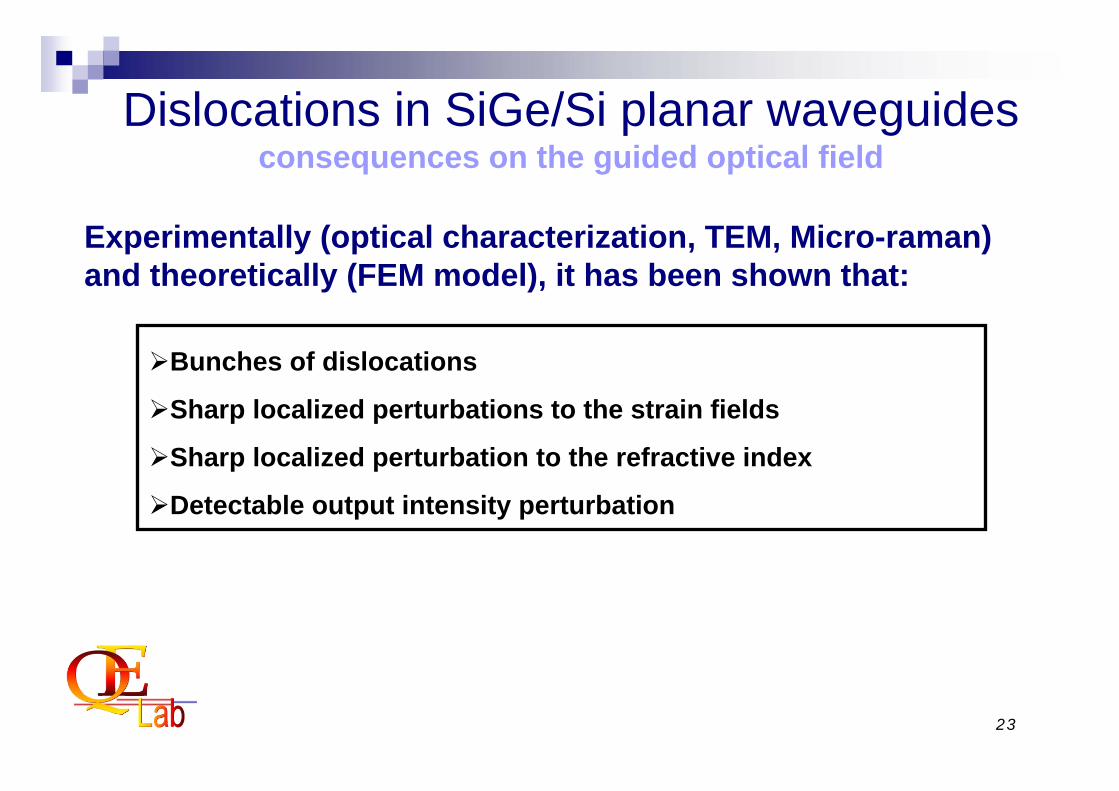
Dislocations in SiGe/Si planar waveguidesconsequences on the guided optical field
Bunches of dislocations
Experimentally (optical characterization, TEM, Micro-raman) and theoretically (FEM model), it has been shown that:

21
Dislocations in SiGe/Si planar waveguidesconsequences on the guided optical field
Bunches of dislocations
Sharp localized perturbations to the strain fields
Experimentally (optical characterization, TEM, Micro-raman) and theoretically (FEM model), it has been shown that:

22
Dislocations in SiGe/Si planar waveguidesconsequences on the guided optical field
Bunches of dislocations
Sharp localized perturbations to the strain fields
Sharp localized perturbation to the refractive index
Experimentally (optical characterization, TEM, Micro-raman) and theoretically (FEM model), it has been shown that:
23
Dislocations in SiGe/Si planar waveguidesconsequences on the guided optical field
Bunches of dislocations
Sharp localized perturbations to the strain fields
Sharp localized perturbation to the refractive index
Detectable output intensity perturbation
Experimentally (optical characterization, TEM, Micro-raman) and theoretically (FEM model), it has been shown that: