Embed Size (px)
Citation preview

Chapter 6
© 2012 Patel and Benedict, licensee InTech. This is an open access chapter distributed under the terms of the Creative Commons Attribution License (http://creativecommons.org/licenses/by/3.0), which permits unrestricted use, distribution, and reproduction in any medium, provided the original work is properly cited.
Crystals in Materials Science
Dinesh G. (Dan) Patel and Jason B. Benedict
Additional information is available at the end of the chapter
http://dx.doi.org/10.5772/50791
1. Introduction
Intense and sustained research into single crystals and polycrystalline assemblies continues
to produce advanced materials crucial to the function of modern and future electronic and
photonic devices. Device function is not only based upon the optical and electronic
properties of the active material (for example, the light absorbing layer in molecular solar
cells), but also the molecular and supramolecular ordering. Herein we will focus on devices
and technologies where single crystalline materials are employed, and where appropriate,
discuss competing materials and devices where polycrystalline or amorphous materials are
used. We acknowledge that there is a sustained push to use solution processable conjugated
polymer films for several similar technological applications; however, these films are
typically disordered and suffer from impurities and chemical defects inherent to synthetic
macromolecules making definitive characterization using X-ray diffraction difficult or
impossible. Small molecule crystalline materials, on the other hand, can be obtained in high
purity with a high level of organization in the solid state.
Additionally, our discussion will be largely limited to organic materials as there is a drive to
replace conventional inorganic active materials (for example the semiconductor channel
layers in transistors) with organic compounds. The reasoning for this lies in the fact that
organic compounds can be synthesized and purified relatively easily using bench-top
techniques without the requirement of high temperatures and energy intensive processes.
As an example, to obtain electronics and solar cell grade silicon several high temperature
steps are required to reach the necessary purities in excess of 99.9999%.1 Organic
compounds can be highly purified using conventional solution crystallization or vapor
growth2 methods yielding materials which exhibit impressive performance, in some cases
rivaling their inorganic counterparts.3
For this review we selected to focus on two areas: (i) photochromic molecules that can be used
for molecular scale data storage and as actuators capable of turning molecular level changes
into macroscopic motion, (ii) organic field effect transistors and organic photovoltaics that

Recent Advances in Crystallography 126
make use of single crystals for charge transport. Other important areas of research such as
catalysis, nonlinear optics, magnetic materials, and biology also make effective use of
crystalline materials but are beyond the scope of this review.
2. Photochromic materials
Photochromism is the light induced reversible change in the absorption spectrum of a
molecule and is necessarily accompanied by changes in both electronic and molecular
structure and properties.4 A generic photochromic system in which component A can be
transformed into B via irradiation with light of energy hν1 is illustrated in Figure 1. Species B
reverts back to A upon exposure to light with energy hν2. As photochromic molecules have
the ability to optically cycle between two spectroscopically distinct states, they have been
studied for possible applications in molecular switching, variable transmission lenses, and
molecular scale optical data storage.5 In some cases a system may also have a thermally
activated pathway for the interconversion of the chemical species. Given the close packing
and perceived rigidity of crystalline lattices, photochromism in the crystalline state was
thought to be rare compared to observation of this phenomenon in solution6 or in polymer
matrices7 where the medium is less constrained and thus permits the associated changes in
molecular shape and volume.
Figure 1. Photochromic compounds can interconvert by irradiation with light of different wavelengths.
The two components, A and B, of a system have different absorption spectra. Though not specifically
shown, a thermal pathway to interconversion may be present.
The spirooxazine (SO) and spiropyran (SP) class of photochromic materials are typified by a
heterocyclic ring-closed isomer, the spiro-form, which is usually colorless and dominates the
equilibrium. The isomerization of representative SO and SP compounds is shown in Scheme
1. Irradiation with high-energy UV light leads to cleavage of the C-O bond at the spirocyclic

Crystals in Materials Science 127
carbon giving a ring-opened form, the photomerocyanine form, that is strongly colored
owing to the extended conjugation afforded by planarity and the donor-acceptor character
of the molecule.5, 8 Removal of the UV irradiation source or irradiation with visible light
affects the reverse reaction. While photochromic spiropyrans9 and spirooxazines10 have been
known for some time, photoisomerization has almost exclusively been observed in solution
and in polymer matrices, though recent research suggests that crystalline state
photoisomerization may be more general and thus make SOs and SPs amenable to use in
solid state devices. Understanding and visualizing the structural and electronic changes that
occur upon photoisomerization would be indispensable in aiding the design and fabrication
of SO and SP containing devices and guide the synthesis of new materials.
Scheme 1. General structure of spirooxazines and spiropyrans. Photoisomerization is initiated with UV
light; visible light or heat affects the ring closing reaction.
More than ten years ago, Benard and Yu used UV-Vis absorption measurements to show
that photoisomerization occurred in microcrystalline powders of cationic SO 111 and SPs 2
and 312 shown in Figure 2. This was attributed to the presence of a large iodide counter ion
giving the necessary free space in the crystal lattice along with stabilization of the iminium
cation that was afforded upon ring opening. When examined by X-ray diffraction, however,
the powder patterns showed only small changes suggesting that the observed isomerization
was likely a surface effect and did not occur in the bulk.
Figure 2. Molecular structures of cationic spirooxazines and spiropyrans that show photochromism in
microcrystalline powders.
Arguably, the single crystalline phase is more constrained than microcrystalline powders
giving less room for the large structural changes that are necessary upon ring opening and
planarization in SOs and SPs. When the indoline group typically used for spirooxazines is
replaced with an azahomoadamantyl group as in SO 4 (Figure 3), isomerization was found
to occur at room temperature in prism shaped single crystals grown from a hexanes
solution.13 The initially colorless, block shaped crystals turned dark purple upon irradiation
with UV light. Unlike in solution, the thermal reaction leading to color bleaching was not
observed in the single crystal, and the dark purple color persisted for several months
compared to seconds or minutes in solution. Analysis of the electron density difference map

Recent Advances in Crystallography 128
(Figure 3c) showed only small changes indicating that there was likely much less than 10%
photoconversion within the crystal.14 The polarized absorption spectra before and after
irradiation (Figure 3d) illustrate the dramatic changes in the absorption spectra that occur
upon photoisomerization. These results demonstrate that crystalline SO materials could be
used as filter materials and possibly as data storage media where the differences in
absorption could correspond to the 1’s and 0’s of the binary computer language. It should be
noted that changes in the polarizer orientation do not lead to significant changes in
absorption because of the orthogonal arrangement of molecules in the crystal lattice.13 The
exact structure of species responsible for the purple color was never discussed, although it
may be some ring opened form that is not completely planar through the conjugated portion
and that may not be able to revert to the closed form owing to crystal packing forces.
Figure 3. (a) Molecular structure and photoisomerization of SO 4, (b) crystal structure of SO 4, (c) the
electron density difference map of a single crystal of 4 before and after irradiation with UV light, and (c)
polarized absorption spectra of 4 before UV irradiation with the polarizer at 0° (red circles) and 90°
(black circles), and after irradiation with the polarizer at 0° (purple squares) and 90° (blue squares)
relative to the [011] plane. The electron density difference map is defined as the difference between the
electron density map of an irradiated single crystal and that of the same crystal before irradiation.
Thermal ellipsoids are shown at the 50% probability level with hydrogens omitted for clarity. (Figure
adapted from reference 13. Reproduced by permission of The Royal Society of Chemistry).
Harada and coworkers15 reported similar results for the irradiation of single crystals,
obtained from methanol or acetone solution, of a series of structurally related SOs and SPs at
various temperatures. UV irradiation at room temperature resulted in little or no color
changes. In contrast, irradiation of the single crystals at 90 K led to strong color changes that
persisted. The population of the photogenerated form was low, however, as it could not be
detected by X-ray diffraction. The supposition was made that the thermal reversion to the
colorless spirocyclic form is fast at room temperature and thus cryogenic temperatures
essentially prevent this reaction. The authors note that it is unclear whether these single
crystal photoreactions occur at defect sites or whether lattice control is directly responsible
and investigations to answer this question are currently underway.
In contrast to the spirooxazine and spiropyran class of photochromic materials,
diarylethenes require only modest structural changes upon photoisomerization. The
observed isomerization is typically not thermally reversible if aryl groups with low aromatic
stabilization energy such as thiophene, benzothiophene, furan, and thiazole are used.18
Crystals in Materials Science 129
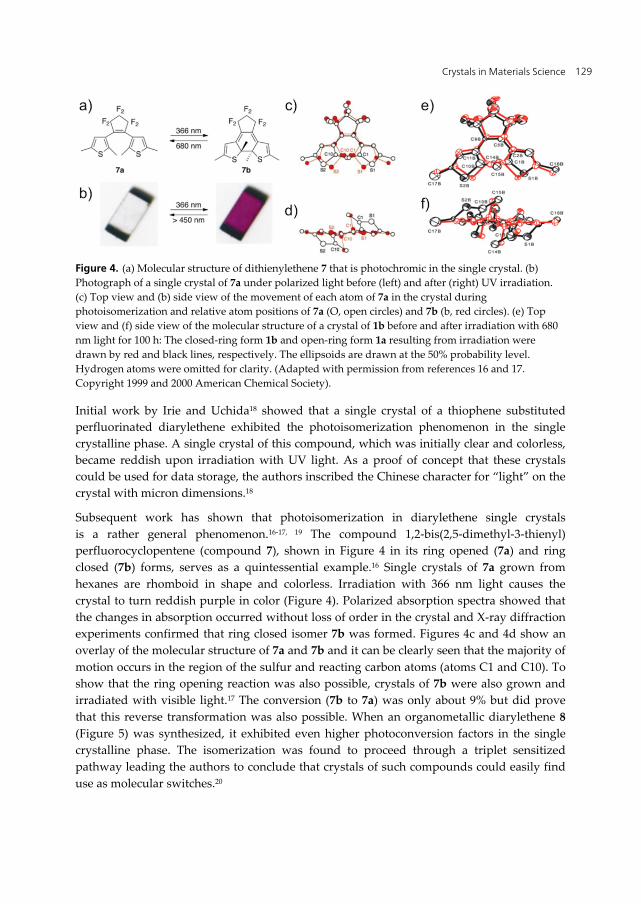
Figure 4. (a) Molecular structure of dithienylethene 7 that is photochromic in the single crystal. (b)
Photograph of a single crystal of 7a under polarized light before (left) and after (right) UV irradiation.
(c) Top view and (b) side view of the movement of each atom of 7a in the crystal during
photoisomerization and relative atom positions of 7a (O, open circles) and 7b (b, red circles). (e) Top
view and (f) side view of the molecular structure of a crystal of 1b before and after irradiation with 680
nm light for 100 h: The closed-ring form 1b and open-ring form 1a resulting from irradiation were
drawn by red and black lines, respectively. The ellipsoids are drawn at the 50% probability level.
Hydrogen atoms were omitted for clarity. (Adapted with permission from references 16 and 17.
Copyright 1999 and 2000 American Chemical Society).
Initial work by Irie and Uchida18 showed that a single crystal of a thiophene substituted
perfluorinated diarylethene exhibited the photoisomerization phenomenon in the single
crystalline phase. A single crystal of this compound, which was initially clear and colorless,
became reddish upon irradiation with UV light. As a proof of concept that these crystals
could be used for data storage, the authors inscribed the Chinese character for “light” on the
crystal with micron dimensions.18
Subsequent work has shown that photoisomerization in diarylethene single crystals
is a rather general phenomenon.16-17, 19 The compound 1,2-bis(2,5-dimethyl-3-thienyl)
perfluorocyclopentene (compound 7), shown in Figure 4 in its ring opened (7a) and ring
closed (7b) forms, serves as a quintessential example.16 Single crystals of 7a grown from
hexanes are rhomboid in shape and colorless. Irradiation with 366 nm light causes the
crystal to turn reddish purple in color (Figure 4). Polarized absorption spectra showed that
the changes in absorption occurred without loss of order in the crystal and X-ray diffraction
experiments confirmed that ring closed isomer 7b was formed. Figures 4c and 4d show an
overlay of the molecular structure of 7a and 7b and it can be clearly seen that the majority of
motion occurs in the region of the sulfur and reacting carbon atoms (atoms C1 and C10). To
show that the ring opening reaction was also possible, crystals of 7b were also grown and
irradiated with visible light.17 The conversion (7b to 7a) was only about 9% but did prove
that this reverse transformation was also possible. When an organometallic diarylethene 8
(Figure 5) was synthesized, it exhibited even higher photoconversion factors in the single
crystalline phase. The isomerization was found to proceed through a triplet sensitized
pathway leading the authors to conclude that crystals of such compounds could easily find
use as molecular switches.20
Recent Advances in Crystallography 130
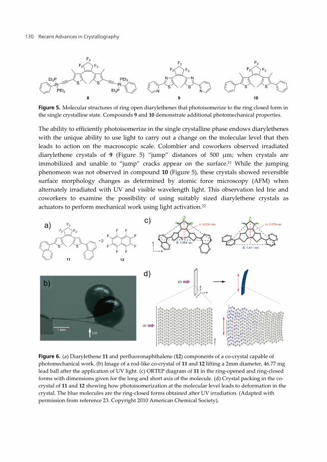
Figure 5. Molecular structures of ring open diarylethenes that photoisomerize to the ring closed form in
the single crystalline state. Compounds 9 and 10 demonstrate additional photomechanical properties.
The ability to efficiently photoisomerize in the single crystalline phase endows diarylethenes
with the unique ability to use light to carry out a change on the molecular level that then
leads to action on the macroscopic scale. Colombier and coworkers observed irradiated
diarylethene crystals of 9 (Figure 5) “jump” distances of 500 μm; when crystals are
immobilized and unable to “jump” cracks appear on the surface.21 While the jumping
phenomeon was not observed in compound 10 (Figure 5), these crystals showed reversible
surface morphology changes as determined by atomic force microscopy (AFM) when
alternately irradiated with UV and visible wavelength light. This observation led Irie and
coworkers to examine the possibility of using suitably sized diarylethene crystals as
actuators to perform mechanical work using light activation.22
Figure 6. (a) Diarylethene 11 and perfluoronaphthalene (12) components of a co-crystal capable of
photomechanical work. (b) Image of a rod-like co-crystal of 11 and 12 lifting a 2mm diameter, 46.77 mg
lead ball after the application of UV light. (c) ORTEP diagram of 11 in the ring-opened and ring-closed
forms with dimensions given for the long and short axis of the molecule. (d) Crystal packing in the co-
crystal of 11 and 12 showing how photoisomerization at the molecular level leads to deformation in the
crystal. The blue molecules are the ring-closed forms obtained after UV irradiation. (Adapted with
permission from reference 23. Copyright 2010 American Chemical Society).

Crystals in Materials Science 131
Initial attempts using single component rod-like crystals22 or co-crystals consisting of a 1:2
molar ratio of diarylethene 11 and perfluonaphthalene (12)23 demonstrated that
photomechanical work was possible as the crystals were able to move a small load upon
irradiation (Figure 6). When a rod-like crystal holding a small lead bearing was irradiated
with UV light, the crystal bent away from the light source lifting the attached weight in the
process. This effect is attributed to the change in the length of the short axis of the molecule
(Figure 6c); when the molecules on the surface of the crystal are irradiated and
photoisomerize to their ring closed state the net effect is an expansion on one side of the
crystal (Figure 6d) which manifests as the macro-scale bending observed. The co-crystals
proved quite durable by withstanding a few hundred cycles without degrading compared
to less than one hundred cycles for the single component crystals.
Recent literature reports indicate that macroscopic motion due to molecular scale
photoisomerization reactions is not unique to the diarylethene class of photochromes. A
dimethylamino-subsistuted azobenzene, compound 13 in Figure 7, was shown to exhibit
crystal bending despite the fact that a large change in molecular geometry is required upon
photoisomerization, namely a trans cis rearrangement.24 Another compound worth
mentioning is salicylideneaniline 14, which has been known to undergo tautomerization in
single crystals.14 Small plate-like microcrystals (73 x 4.5 x 1.1 μm) were grown by
sublimation, and when irradiated with 365 nm light bent in a direction away from the light
source.25 Irradiation with visible light returned the crystals to their former position. X-ray
diffraction experiments confirmed that approximately 10% of the molecules had
photoisomerized. Thus, it has been hypothesized that photochromic actuators could find
use in artificial muscles and devices where light initiated photoisomerization is effectively
translated into macroscopic motion.
Figure 7. The molecular structures of photochromic azobenzene 13 and salicylideneaniline 14. Both
compounds show photomechanical effects in the single crystalline state.
In addition to mechanical and optical effects, the change in bonding pattern associated with
the photoisomerization process has been explored as related to its influence on magnetic
properties. In particular, the differences in conjugation between the two components of a
photochromic system containing magnetic centers can lead to switchability in magnetic
properties. Magnetism arises from the motion of charge, in particular unpaired electrons.
Therefore, metal ions or organic radicals are typically employed and the resulting magnetic
properties explored using single crystalline or microcrystalline materials.
Using the highly versatile diarylethene molecular framework, Irie showed that coupling
between two terminal nitronyl nitroxide radical groups depended on whether the
diarylethene was in its ring opened or ring closed form.26 Microcrystalline powders of the
Recent Advances in Crystallography 132
ring opened form showed little coupling between the two nitronyl nitroxide radicals, while
the ring closed form showed strong anti-ferromagnetic coupling. This was attributed to the
ability of the radicals to delocalize over the π-system, which was in turn dependent on
whether the molecule was in its ring opened or ring closed state.
A relatively new means of controlling the magnetic properties of a material relies on the
interaction between a metal center with unpaired electrons and a photoisomerizable
ligand.27 The ligand field, which in turn affects the magnetic behavior of the metal electrons,
is predicted to change upon isomerization from one photochromic state to another. This has
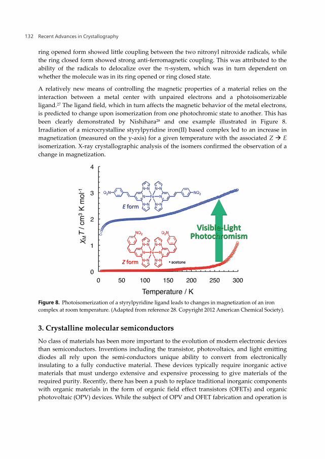
been clearly demonstrated by Nishihara28 and one example illustrated in Figure 8.
Irradiation of a microcrystalline styrylpyridine iron(II) based complex led to an increase in
magnetization (measured on the y-axis) for a given temperature with the associated Z E
isomerization. X-ray crystallographic analysis of the isomers confirmed the observation of a
change in magnetization.
Figure 8. Photoisomerization of a styrylpyridine ligand leads to changes in magnetization of an iron
complex at room temperature. (Adapted from reference 28. Copyright 2012 American Chemical Society).
3. Crystalline molecular semiconductors
No class of materials has been more important to the evolution of modern electronic devices
than semiconductors. Inventions including the transistor, photovoltaics, and light emitting
diodes all rely upon the semi-conductors unique ability to convert from electronically
insulating to a fully conductive material. These devices typically require inorganic active
materials that must undergo extensive and expensive processing to give materials of the
required purity. Recently, there has been a push to replace traditional inorganic components
with organic materials in the form of organic field effect transistors (OFETs) and organic
photovoltaic (OPV) devices. While the subject of OPV and OFET fabrication and operation is

Crystals in Materials Science 133
beyond the scope of this review, it is worth mentioning that one of the most important
properties of a semiconducting material is its ability to conduct charge (referred to as the
mobility and given in units of cm2/Vs), either electrons or holes, and this is highly
dependent on electronic structure, energy level (HOMO/LUMO) position, and on
supramolecular organization.29 Both π-conjugated polymers and small molecule based
compounds have been examined, but only the molecular materials can be obtained in the
required purity with the required supramolecular order that gives rise to the necessary
charge transport properties.30 The acene class of molecules shown in Figure 9 are among the
most widely studied and best performing materials with regard to charge conductivity.31
Figure 9. The structure of commonly used acene small molecules.
Facile processing is one of the greatest advantages organic materials hold over their
inorganic counterparts. Organic molecules can be deposited on substrates in a number of
ways including spin coating from solution, dip coating, vapor deposition methods, and ink-
jet printing. The best performing materials are grown using the vapor deposition method,2b
illustrated in Figure 10a, which can afford high quality single crystals while removing
unwanted contaminants.2a, 32 The single crystals are then manually harvested and
manipulated into the appropriate device architecture. In contrast, dip-coating and other
solution processing methods typically give lower quality materials relative to vapor-grown
crystals (Figure 10b).
Although pentacene (structure show in Figure 9) was a popular molecule for OFET studies,
rubrene (Figure 9) is now growing in popularity due to its superior stability in air as
pentacene is easily oxidized.34 Rubrene is known to exhibit several polymorphs depending on
crystal growth conditions with packing also determined by competition between
quadrupolar and π-stacking interactions.35 It has the ability to form high quality crystals with
an electronic band structure36 as opposed to discrete energy states and was first examined as
a single crystal OFET by Podzorov and coworkers who fabricated devices with mobilities as
high as 1 cm2/Vs37 and up to 20 cm2/Vs with an optimized device.38 Soon after, Brédas and
coworkers compared the crystalline state structures of rubrene to unsubstituted acenes both
computationally and experimentally and found that, contrary to expectation, the bulky
phenyl side groups force molecular displacements that promote large intermolecular
electronic coupling.39 Furthermore, mobility was shown to be axially dependent.40 However,
when an “in channel” device was fabricated, where charge carriers moved through the bulk
of the crystal as opposed to near the surface, mobility values of ~40 cm2/Vs were obtained

Recent Advances in Crystallography 134
Figure 10. A schematic showing (a) the physical vapor transport method of single crystal growth
contrasted with the (b) growth of crystals by solution methods. The physical vapor transport method
offers crystals of high purity and greater uniformity. (Figure taken from reference 33 with permission).
thus showing that surface traps and adsorbed impurities greatly impact OFET performance.
More importantly, the high mobilities measured in these materials indicate that organic
single crystals are suitable for use in electronic devices.
Andrienko and coworkers41 have suggested, that single crystal based OFETS may not be
practical, likely owing to the delicate manipulations needed to make the devices coupled
with the fragile nature of the crystals. Anthony and coworkers31a, b, 42 have tried to
synthesize acenes with solubilizing groups that can be deposited using solution methods
while maintaining a high level of crystalline order. Examples of these soluble acenes are
shown in Figure 11. Some of the derivatives show good mobilities (on the order of 1.0
cm2/Vs) for solution-processed materials. Interestingly, small changes in the solubilizing
groups lead to pronounced changes in the crystal packing as determined by X-ray
diffraction. A triethylsilyl substituted acene (compound 16) exhibited a brick-work31c
packing motif that is ideal for maximized π-orbital overlap between neighboring molecules
which translated into mobilities of 1.0 cm2/Vs. A simple switch from the triethyl to the
trimethylsilyl substituted acene (compound 17) resulted in crystal structure that exhibited
herringbone packing, negligible intermolecular orbital overlap, and mobilities that were
too low to be measured.
Given the interest in making high quality single crystals or crystalline films of organic
semiconductors for OFETs, new methods have emerged for the deposition of such
structures. Inkjet printing techniques43 have been shown to give microcrystals capable of

Crystals in Materials Science 135
Figure 11. Crystal structure of anthradithiophenes 15 – 16 and their corresponding crystal structures.
The alkyl groups on the front-most silicon atoms have been omitted for clarity. (Adapted with
permission from reference 42c. Copyright 2005 American Chemical Society).
diffracting X-rays and giving diffraction patterns similar to bulk materials. This was
achieved by inkjet printing a solution of the semiconductor in close proximity to a droplet of
an antisolvent leading to slow crystallization as the solvents mix and evaporate. The crystals
of a benzothiophene-based molecule obtained using this technique exhibit average
mobilities of 16.4 cm2/Vs which are similar to that of rubrene single crystal devices.
The Bao group has actively been pursuing OFET technologies and has introduced patterned
growth techniques that have the potential to grow crystals directly on devices obviating the
need for manual manipulation of delicate crystals as is required in the vapor growth
method.44 Patterned growth is achieved by using a pre-patterned, self assembled monolayer
as a growth template. Takeya and coworkers have introduced an oriented growth method3,
45 where an inclined substrate and a “liquid-sustaining piece” allow high quality crystals to
form on a SiO2 coated substrate. The resulting materials were single crystalline as confirmed
by X-ray diffraction and gave mobilities on the order of 2 – 6 cm2/Vs. Thus, it can be seen
that high quality single crystals with good mobility characteristics can be obtained by
solution methods.

Recent Advances in Crystallography 136
Figure 12. (a) The molecular structure of α-furan hexamer 10 and its crystal packing (b) and (c). The
values given in parenthesis are for the thiophene analogue. (Adapted with permission from reference
46. Copyright 2010 American Chemical Society).
While significant effort has gone into new methods of growing high quality crystals and
improving the solubility of acenes known to exhibit good performance in OFETs, effort is
also directed toward the design of new materials with improved properties, such as smaller
intramolecular distances in the solid state, that would lead to improved mobilities. While
attention has been focused largely on thiophene based compounds47 a recent report by
Bendikov and coworkers46 used X-ray crystallography, among other techniques, to
reexamine the solid state structure of furan based materials. In particular, they synthesized
and studied a series of furan oligomers including α-furan hexamer 10, the structure and
crystal packing of which is shown in Figure 12. When compared to the thiophene
analogue,48 10 was found to exhibit closer packing (2.57 Å for 10 versus 2.89 Å for the
thiophene analogue) and shorter inter-ring C-C bond distances indicating less aromatic
character and more quinoidal character, both of which could facilitate better charge
transport in furan-based materials. The Bendikov group has also explored OFETs from
oligofuran materials,49 and a recent study showed that solution grown crystals of a
naphthodifuran gave mobilities of 3.6 cm2/Vs despite exhibiting herringbone packing,
which leads to less than optimal intermolecular π-orbital overlap.50 Thus, it appears that
furan based crystalline semiconductors, with further optimization and crystal engineering,
could eventually surpass their thiophene analogues.
Given the high mobilities intrinsic to single crystalline acene type semiconductors, it would
seem that single crystalline materials would be well suited for OPVs, which similar to
OFETs, require high mobility materials, but also require materials able to efficiently absorb
solar energy. There are, however, few examples of single crystal organic photovoltaics51 as
most research is devoted to polymeric materials,52 solution processable small molecule
semiconductors,53 and dye-sensitized solar cells.54 Recently, Yang and coworkers assembled

Crystals in Materials Science 137
a solar cell based on a single crystal of tetracene (shown in Figure 9) as the light absorbing
layer and a C60 electron transport layer.55 The device showed efficiencies that were less than
1%, and efficiency depended critically on the thickness of the crystal used in addition to the
crystal face that was irradiated. The authors hypothesized that the device suffered from low
performance because of the poor absorption of visible light by tetracene. Campione and
coworkers similarly, examined single crystal photovoltaic devices based on rubrene,
perylene, α-quarterthiophene, and tetracene without employing a C60 layer. While the
voltage generated by the cell was adequate, the current generated was very low giving
efficiencies that were on the order of 10-5%. The authors attribute the low performance to a
high rate of exciton recombination, which they say does not necessarily preclude the use of
single crystals in solar cells, but may necessitate the use of electron accepting materials to
ensure a higher propensity for exciton separation in the active layer. Higher efficiencies
have been obtained using organic materials; Kippelen and coworkers achieved an efficiency
of ~2.7 % using a cell consisting of pentacene and C60, however, the active layer was
polycrystalline.56
Figure 13. The molecular structure of TA-PPE.
Single crystal based devices show impressive mobilities, yet are not suitable for use when
larger surface area coverage is desired such as in manufacturing displays and some solar
cells, both of which are intensely pursued by academic and industrial groups seeking to
commercialize these technologies. Polymeric and molecular materials amenable to spin
coating and spray coating methods are ideally suited for coverage of large areas, but the
mobilities resulting from amorphous and polycrystalline morphologies are orders of
magnitude lower than those obtained for small single crystals. In an effort to close this gap,
self-assembly processes have been examined for the generation of morphologies conducive
to good charge transport and concomitant application in large area devices. In particular,
nano-scale wires based on organic materials have been shown to be highly crystalline in
nature, thus translating into effective charge transport materials57 using simple and
inexpensive solution methods.
Conjugated polymer nanowires with the potential for high mobility have been observed,
although polymeric materials are typically spin coated or spray coated from dilute solutions
giving amorphous films after solvent evaporation. In a prototypical example, however,
careful and controlled deposition of the polymer TA-PPE (Figure 13) gave crystalline
nanowires.58 These nanowires were obtained by slow evaporation (over a period of days) of
a tetrahydrofuran solution of polymer with concentrations ranging from 0.05 – 0.10 mg/mL.
When incorporated into an OFET, the nanowires exhibited mobilities on the order of 0.01 –

Recent Advances in Crystallography 138
0.1 cm2/Vs, which were 3 – 4 orders of magnitude higher than the mobilities obtained from
an amorphous film of TA-PPE obtained by spin coating. The slow evaporation ensured
good ordering of the polymer wires as shown in Figure 14. Selected Area Electron
Diffraction (SAED) gave sharp diffraction peaks indicating a high level of order as
manifested in the high mobility values. Thus, conditions that allow polymer units to
organize into higher order morphologies may be broadly applicable.
Figure 14. (a) TEM image of an individual TA-PPE nanowire (scale bar: 150 nm) and (b) its
corresponding SAED pattern. (c) Schematic diagram of possible molecular packing in the one-
dimensional nanowires; for clarity the end-capping groups have been omitted. (Adapted with
permission from reference 58. Copyright 2009 American Chemical Society).
Molecular materials with a propensity to form ordered, π-stacks have also demonstrated the
ability to form crystalline molecular wires. A dianthracene diester gave crystals that packed
with good π-overlap between neighboring anthracene units.59 Crystalline nanorods, when
irradiated with UV light, underwent a [2+2] photopolymerzation reaction in a crystal-to-
crystal type transformation. While the resulting polymer was not well suited to charge
transport, the authors clearly demonstrated how single crystalline nanorods could be used
to give other materials with application in organic electronics. In a similar study, a
dicyanovinyl substituted anthracene molecule formed nanowires when films were cast from
dichloromethane solution. These nanowires gave remarkably clear SAED patterns proving
the single crystalline organization of the component molecules. Moreover, while the
Crystals in Materials Science 139
mobility properties were not measured, the nanowires exhibit photoswitchable conductivity
potentially allowing their use in photodetectors.
For most electronic applications, crystalline organic compounds still lag behind their
inorganic counterparts in terms of device performance; however, the gap has been steadily
decreasing. Given the continuous rapid advances of organic crystalline semiconductors,
these materials may soon replace traditional inorganics and usher in an era of carbon-based
electronic devices.
Author details
Dinesh G. (Dan) Patel and Jason B. Benedict
Department of Chemistry, State University of New York at Buffalo, Buffalo, New York, USA
4. References
[1] (a) Braga, A. F. B.; Moreira, S. P.; Zampieri, P. R.; Bacchin, J. M. G.; Mei, P. R., Sol. Energy
Mater. Sol. Cells 2008, 92 (4), 418-424; (b) Mei, P. R.; Moreira, S. P.; Cardoso, E.; Cortes, A.
D. S.; Marques, F. C., Sol. Energy Mater. Sol. Cells 2012, 98, 233-239; (c) Taft, E. A.; Horn,
F. H., J. Electrochem. Soc. 1958, 105 (2), 81-83.
[2] (a) Kloc, C.; Simpkins, P. G.; Siegrist, T.; Laudise, R. A., J. Cryst. Growth 1997, 182 (3-4),
416-427; (b) Laudise, R. A.; Kloc, C.; Simpkins, P. G.; Siegrist, T., J. Cryst. Growth 1998,
187 (3-4), 449-454.
[3] Uemura, T.; Hirose, Y.; Uno, M.; Takimiya, K.; Takeya, J., Applied Physics Express 2009, 2
(11), 111501.
[4] Dürr, H.; Bous-Laurent, H., Photochromism: Molecules and Systems. Elsevier: Amsterdam,
1990.
[5] Crano, J. C.; Guglielmetti, R. J., Organic Photochromic and Thermochromic Compounds.
Plenum Press: New York, 1999.
[6] Dürr, H.; Bouas-Laurent, H., Photochromism : molecules and systems. Rev. ed.; Elsevier:
Amsterdam ; Boston, 2003; p liii, 1044 p.
[7] (a) Evans, R. A.; Hanley, T. L.; Skidmore, M. A.; Davis, T. P.; Such, G. K.; Yee, L. H.; Ball,
G. E.; Lewis, D. A., Nat. Mater. 2005, 4 (3), 249-253; (b) Evans, R. A.; Such, G. K., Aust. J.
Chem. 2005, 58 (12), 825-830; (c) Such, G. K.; Evans, R. A.; Davis, T. P., Macromolecules
2004, 37 (26), 9664-9666; (d) Such, G. K.; Evans, R. A.; Davis, T. P., Macromolecules 2006,
39 (4), 1391-1396.
[8] Patel, D. G.; Paquette, M. M.; Kopelman, R. A.; Kaminsky, W.; Ferguson, M. J.; Frank, N.
L., J. Am. Chem. Soc. 2010, 132 (36), 12568-12586.
[9] Hirshberg, Y., J. Am. Chem. Soc. 1956, 78 (10), 2304-2312.
[10] Chu, N. Y. C., Can. J. Chem. 1983, 61 (2), 300-305.
[11] Bénard, S.; Yu, P., Chem. Commun. 2000, (1), 65-66.
[12] Bénard, S.; Yu, P., Adv. Mater. 2000, 12 (1), 48-50.
Recent Advances in Crystallography 140
[13] Patel, D. G.; Benedict, J. B.; Kopelman, R. A.; Frank, N. L., Chem. Commun. 2005, (17),
2208-2210.
[14] Harada, J.; Uekusa, H.; Ohashi, Y., J. Am. Chem. Soc. 1999, 121 (24), 5809-5810.
[15] Harada, J.; Kawazoe, Y.; Ogawa, K., Chem. Commun. 2010, 46 (15), 2593-2595.
[16] Kobatake, S.; Yamada, T.; Uchida, K.; Kato, N.; Irie, M., J. Am. Chem. Soc. 1999, 121 (11),
2380-2386.
[17] Yamada, T.; Kobatake, S.; Muto, K.; Irie, M., J. Am. Chem. Soc. 2000, 122 (8), 1589-1592.
[18] Irie, M.; Uchida, K., Bull. Chem. Soc. Jpn. 1998, 71 (5), 985-996.
[19] (a) Kobatake, S.; Hasegawa, H.; Miyamura, K., Cryst. Growth. Des. 2011, 11 (4), 1223-
1229; (b) Kobatake, S.; Kuma, S.; Irie, M., J. Phys. Org. Chem. 2007, 20 (11), 960-967; (c)
Liu, G.; Liu, M.; Pu, S.; Fan, C.; Cui, S., Tetrahedron 2012, 68 (10), 2267-2275; (d) Liu, G.;
Pu, S.; Wang, X., Tetrahedron 2010, 66 (46), 8862-8871; (e) Matsuda, K.; Takayama, K.;
Irie, M., Inorg. Chem. 2003, 43 (2), 482-489; (f) Ohara, H.; Morimoto, M.; Irie, M.,
Photochem. Photobiol. Sci. 2010, 9 (8), 1079-1081; (g) Pu, S.; Liu, G.; Shen, L.; Xu, J., Org.
Lett. 2007, 9 (11), 2139-2142.
[20] Brayshaw, S. K.; Schiffers, S.; Stevenson, A. J.; Teat, S. J.; Warren, M. R.; Bennett, R. D.;
Sazanovich, I. V.; Buckley, A. R.; Weinstein, J. A.; Raithby, P. R., Chem. Eur. J. 2011, 17
(16), 4385-4395.
[21] Colombier, I.; Spagnoli, S.; Corval, A.; Baldeck, P. L.; Giraud, M.; Léaustic, A.; Yu, P.,
Mol. Cryst. Liq. Cryst. 2005, 431 (1), 495-499.
[22] Kobatake, S.; Takami, S.; Muto, H.; Ishikawa, T.; Irie, M., Nature 2007, 446 (7137), 778-
781.
[23] Morimoto, M.; Irie, M., J. Am. Chem. Soc. 2010, 132 (40), 14172-14178.
[24] Koshima, H.; Ojima, N.; Uchimoto, H., J. Am. Chem. Soc. 2009, 131 (20), 6890-6891.
[25] Koshima, H.; Takechi, K.; Uchimoto, H.; Shiro, M.; Hashizume, D., Chem. Commun.
2011, 47 (41), 11423-11425.
[26] Matsuda, K.; Irie, M., J. Am. Chem. Soc. 2000, 122 (30), 7195-7201.
[27] (a) Boillot, M.-L.; Chantraine, S.; Zarembowitch, J.; Lallemand, J.-Y.; Prunet, J., New J.
Chem. 1999, 179-183; (b) Boillot, M.-L.; Roux, C.; Audiere, J.-P.; Dausse, A.;
Zarembowitch, J., Inorg. Chem. 1996, 35, 3975-3980; (c) Roux, C.; Zarembowitch, J.;
Gallois, B.; Granier, T.; Claude, R., Inorg. Chem. 1994, 33 (10), 2273.
[28] Takahashi, K.; Hasegawa, Y.; Sakamoto, R.; Nishikawa, M.; Kume, S.; Nishibori, E.;
Nishihara, H., Inorg. Chem. 2012, 51 (9), 5188-5198.
[29] Mas-Torrent, M.; Rovira, C., Chem. Rev. 2011, 111 (8), 4833-4856.
[30] Hoeben, F. J. M.; Jonkheijm, P.; Meijer, E. W.; Schenning, A., Chem. Rev. 2005, 105 (4),
1491-1546.
[31] (a) Anthony, J. E., Chem. Rev. 2006, 106 (12), 5028-5048; (b) Anthony, J. E., Angew. Chem.
Int. Ed. 2008, 47 (3), 452-483; (c) Würthner, F.; Schmidt, R., ChemPhysChem 2006, 7 (4),
793-797.
[32] Jurchescu, O. D.; Baas, J.; Palstra, T. T. M., Appl. Phys. Lett. 2004, 84 (16), 3061-3063.
[33] Reese, C.; Bao, Z., Mater. Today 2007, 10 (3), 20-27.
[34] Hasegawa, T.; Takeya, J., Science and Technology of Advanced Materials 2009, 10 (2).
[35] Jurchescu, O. D.; Meetsma, A.; Palstra, T. T. M., Acta Cryst. B 2006, 62 (2), 330-334.

Crystals in Materials Science 141
[36] Ding, H.; Reese, C.; Makinen, A. J.; Bao, Z.; Gao, Y., Appl. Phys. Lett. 2010, 96 (22), 3.
[37] Podzorov, V.; Pudalov, V. M.; Gershenson, M. E., Appl. Phys. Lett. 2003, 82 (11), 1739-
1741.
[38] Podzorov, V.; Menard, E.; Borissov, A.; Kiryukhin, V.; Rogers, J. A.; Gershenson, M. E.,
Phys. Rev. Lett. 2004, 93 (8), 086602.
[39] da Silva Filho, D. A.; Kim, E. G.; Brédas, J. L., Adv. Mater. 2005, 17 (8), 1072-1076.
[40] Sundar, V. C.; Zaumseil, J.; Podzorov, V.; Menard, E.; Willett, R. L.; Someya, T.;
Gershenson, M. E.; Rogers, J. A., Science 2004, 303 (5664), 1644-1646.
[41] Vehoff, T.; Baumeier, B.; Troisi, A.; Andrienko, D., J. Am. Chem. Soc. 2010, 132 (33),
11702-11708.
[42] (a) Anthony, J. E.; Eaton, D. L.; Parkin, S. R., Org. Lett. 2002, 4 (1), 15-18; (b) Payne, M.
M.; Odom, S. A.; Parkin, S. R.; Anthony, J. E., Org. Lett. 2004, 6 (19), 3325-3328; (c) Payne,
M. M.; Parkin, S. R.; Anthony, J. E.; Kuo, C.-C.; Jackson, T. N., J. Am. Chem. Soc. 2005, 127
(14), 4986-4987; (d) Purushothaman, B.; Bruzek, M.; Parkin, S. R.; Miller, A.-F.; Anthony,
J. E., Angew. Chem. Int. Ed. 2011, 50 (31), 7013-7017.
[43] Minemawari, H.; Yamada, T.; Matsui, H.; Tsutsumi, J.; Haas, S.; Chiba, R.; Kumai, R.;
Hasegawa, T., Nature 2011, 475 (7356), 364-367.
[44] (a) Briseno, A. L.; Aizenberg, J.; Han, Y.-J.; Penkala, R. A.; Moon, H.; Lovinger, A. J.;
Kloc, C.; Bao, Z., J. Am. Chem. Soc. 2005, 127 (35), 12164-12165; (b) Briseno, A. L.;
Mannsfeld, S. C. B.; Ling, M. M.; Liu, S.; Tseng, R. J.; Reese, C.; Roberts, M. E.; Yang, Y.;
Wudl, F.; Bao, Z., Nature 2006, 444 (7121), 913-917.
[45] Soeda, J.; Hirose, Y.; Yamagishi, M.; Nakao, A.; Uemura, T.; Nakayama, K.; Uno, M.;
Nakazawa, Y.; Takimiya, K.; Takeya, J., Adv. Mater. 2011, 23 (29), 3309-3314.
[46] Gidron, O.; Diskin-Posner, Y.; Bendikov, M., J. Am. Chem. Soc. 2010, 132 (7), 2148-2150.
[47] Perepichka, I. F.; Perepichka, D. F., Handbook of thiophene-based materials. Wiley:
Hoboken, 2009.
[48] Horowitz, G.; Bachet, B.; Yassar, A.; Lang, P.; Demanze, F.; Fave, J. L.; Garnier, F., Chem.
Mater. 1995, 7 (7), 1337-1341.
[49] Gidron, O.; Dadvand, A.; Sheynin, Y.; Bendikov, M.; Perepichka, D. F., Chem. Commun.
2011, 47 (7), 1976-1978.
[50] Mitsui, C.; Soeda, J.; Miwa, K.; Tsuji, H.; Takeya, J.; Nakamura, E., J. Am. Chem. Soc.
2012, 134 (12), 5448-5451.
[51] (a) Bredas, J.-L.; Durrant, J. R., Acc. Chem. Res. 2009, 42 (11), 1689-1690; (b) Clarke, T. M.;
Durrant, J. R., Chem. Rev. 2010, 110 (11), 6736-6767.
[52] Günes, S.; Neugebauer, H.; Sariciftci, N. S., Chem. Rev. 2007, 107 (4), 1324-1338.
[53] (a) Dang, X.-D.; Tamayo, A. B.; Seo, J.; Hoven, C. V.; Walker, B.; Nguyen, T.-Q., Adv.
Funct. Mater. 2010, 20 (19), 3314-3321; (b) Roncali, J., Acc. Chem. Res. 2009, 42 (11), 1719-
1730; (c) Tamayo, A. B.; Tantiwiwat, M.; Walker, B.; Nguyen, T.-Q., J. Phys. Chem. C
2008, 112 (39), 15543-15552; (d) Walker, B.; Tamayo, A.; Duong, D. T.; Dang, X. D.; Kim,
C.; Granstrom, J.; Nguyen, T. Q., Advanced Energy Materials 2011, 1 (2), 221-229.
[54] (a) Hagfeldt, A.; Boschloo, G.; Sun, L.; Kloo, L.; Pettersson, H., Chem. Rev. 2010, 110 (11),
6595-6663; (b) Nazeeruddin, M. K.; Kay, A.; Rodicio, I.; Humphry-Baker, R.; Müller, E.;

Recent Advances in Crystallography 142
Liska, P.; Vlachopoulos, N.; Grätzel, M., J. Am. Chem. Soc. 1993, 115 (14), 6382-6390; (c)
O'Regan, B.; Grätzel, M., Nature 1991, 353 (6346), 737-740.
[55] Tseng, R. J.; Chan, R.; Tung, V. C.; Yang, Y., Adv. Mater. 2008, 20 (3), 435-438.
[56] Yoo, S.; Domercq, B.; Kippelen, B., Appl. Phys. Lett. 2004, 85 (22), 5427-5429.
[57] Briseno, A. L.; Mannsfeld, S. C. B.; Jenekhe, S. A.; Bao, Z.; Xia, Y., Mater. Today 2008, 11
(4), 38-47.
[58] Dong, H.; Jiang, S.; Jiang, L.; Liu, Y.; Li, H.; Hu, W.; Wang, E.; Yan, S.; Wei, Z.; Xu, W.;
Gong, X., J. Am. Chem. Soc. 2009, 131 (47), 17315-17320.
[59] Al-Kaysi, R. O.; Dillon, R. J.; Kaiser, J. M.; Mueller, L. J.; Guirado, G.; Bardeen, C. J.,
Macromolecules 2007, 40 (25), 9040-9044.