Embed Size (px)
Citation preview
Digitally Assisted Analog Circuit Design for
Communication SoCs
Teresa Meng, Boris Murmann, and Alok AggarwalDepartment of Electrical Engineering
Stanford University
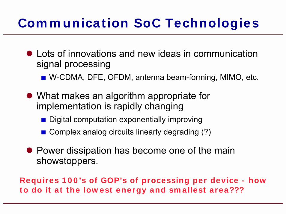
Communication SoC Technologies
! Lots of innovations and new ideas in communication signal processing
W-CDMA, DFE, OFDM, antenna beam-forming, MIMO, etc.
! What makes an algorithm appropriate for implementation is rapidly changing
Digital computation exponentially improvingComplex analog circuits linearly degrading (?)
! Power dissipation has become one of the main showstoppers.
Requires 100’s of GOP’s of processing per device - how to do it at the lowest energy and smallest area???
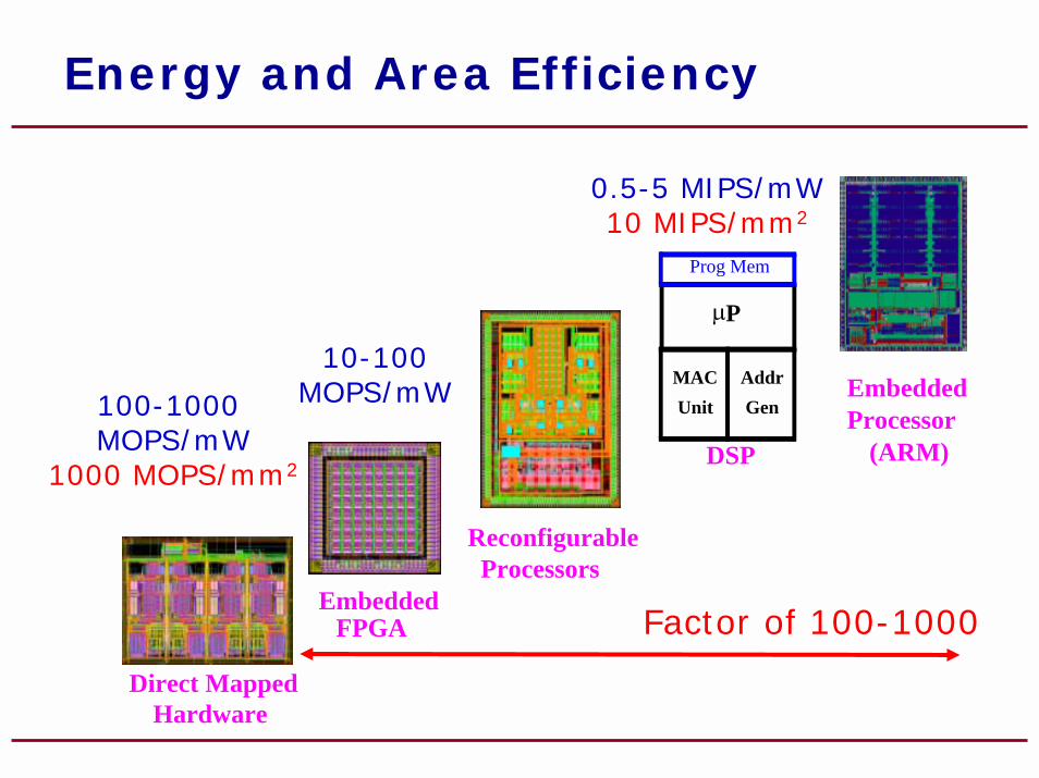
Energy and Area Efficiency
0.5-5 MIPS/mW10 MIPS/mm2
MACUnit
AddrGen
µP
Prog Mem
DSP
Flex
ibili
ty
Embedded Processor
(ARM)
100-1000 MOPS/mW
1000 MOPS/mm2
10-100MOPS/mW
ReconfigurableProcessors
Direct MappedHardware
EmbeddedFPGA Factor of 100-1000
Area or Power
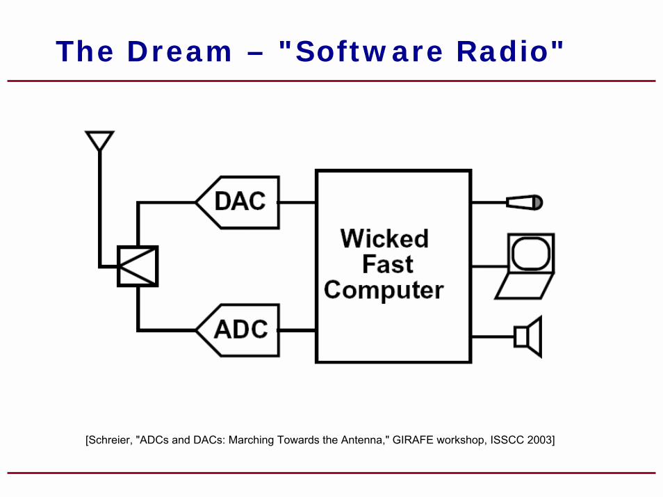
The Dream – "Software Radio"
[Schreier, "ADCs and DACs: Marching Towards the Antenna," GIRAFE workshop, ISSCC 2003]
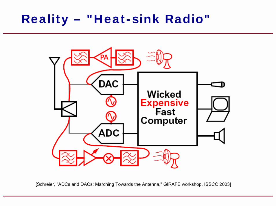
Reality – "Heat-sink Radio"
[Schreier, "ADCs and DACs: Marching Towards the Antenna," GIRAFE workshop, ISSCC 2003]
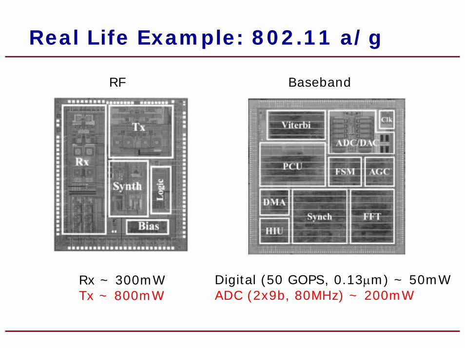
Real Life Example: 802.11 a/g
RF Baseband
Digital (50 GOPS, 0.13µm) ~ 50mWADC (2x9b, 80MHz) ~ 200mW
Rx ~ 300mWTx ~ 800mW
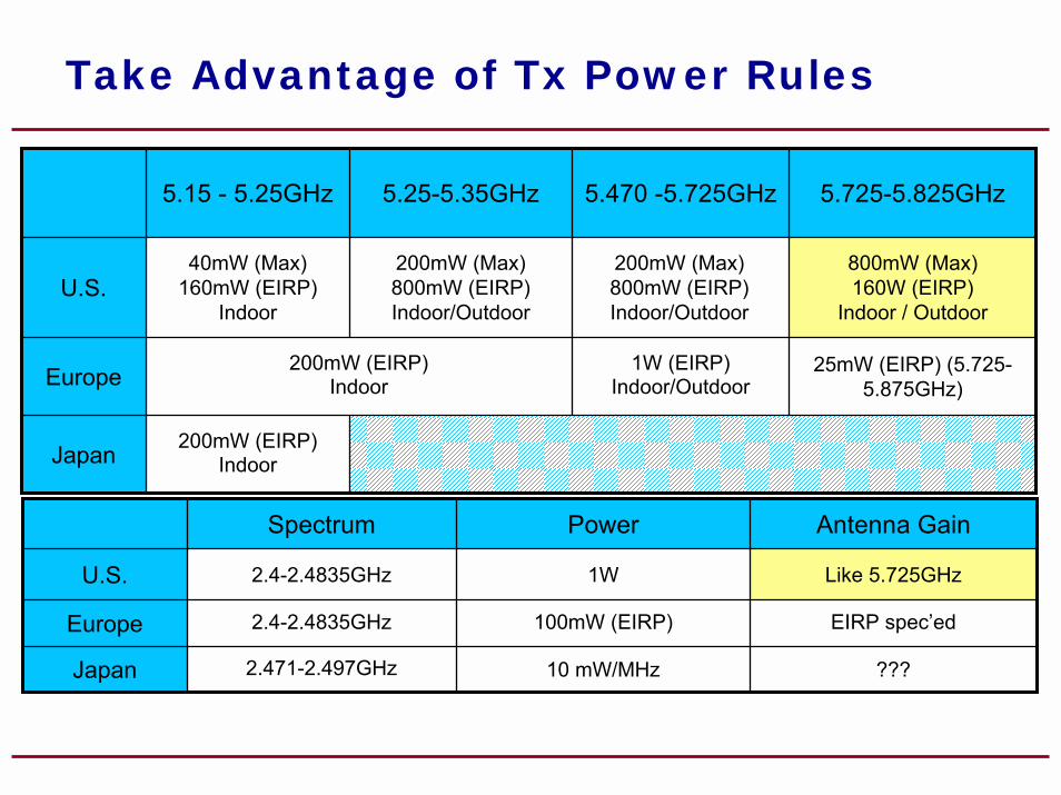
Take Advantage of Tx Power Rules
200mW (EIRP)IndoorJapan
25mW (EIRP) (5.725-5.875GHz)
1W (EIRP)Indoor/Outdoor
200mW (EIRP)IndoorEurope
800mW (Max)160W (EIRP)
Indoor / Outdoor
200mW (Max)800mW (EIRP)Indoor/Outdoor
40mW (Max)160mW (EIRP)
IndoorU.S.
5.725-5.825GHz5.470 -5.725GHz5.25-5.35GHz5.15 - 5.25GHz
200mW (Max)800mW (EIRP)Indoor/Outdoor
100mW (EIRP)
???10 mW/MHz2.471-2.497GHzJapan
EIRP spec�ed2.4-2.4835GHzEurope
Like 5.725GHz1W2.4-2.4835GHzU.S.
Antenna GainPowerSpectrum
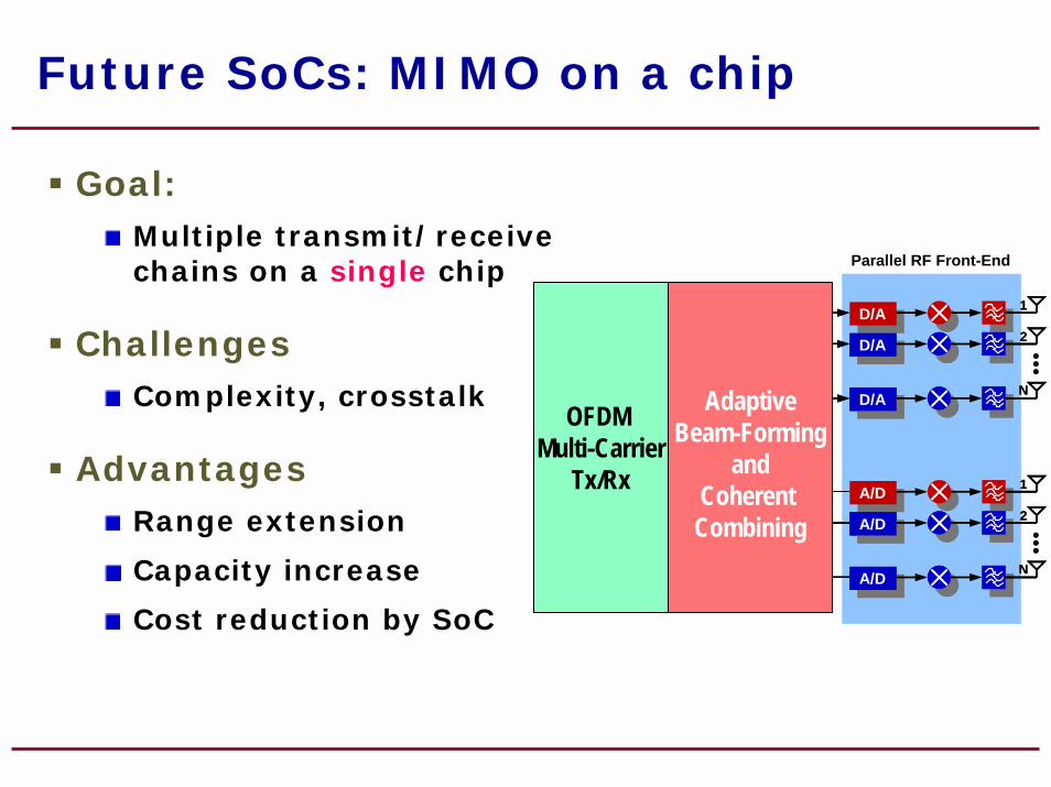
Future SoCs: MIMO on a chip
" Goal: Multiple transmit/receive chains on a single chip
" ChallengesComplexity, crosstalk
" AdvantagesRange extension
Capacity increase
Cost reduction by SoC
D/A
D/AD/A
D/AD/A
1
2
N
1
2
N
A/D
A/DA/D
A/DA/D
1
2
N
1
2
N
Parallel RF Front-End
AdaptiveBeam-Forming
andCoherent
Combining
OFDM Multi-Carrier
Tx/Rx
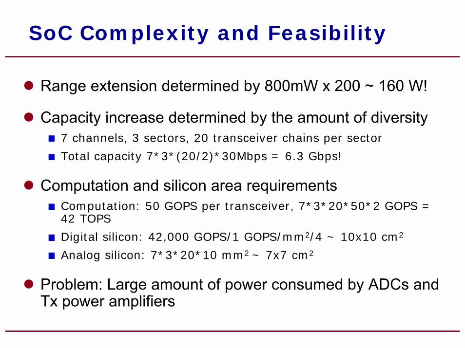
SoC Complexity and Feasibility
! Range extension determined by 800mW x 200 ~ 160 W!
! Capacity increase determined by the amount of diversity7 channels, 3 sectors, 20 transceiver chains per sector
Total capacity 7*3*(20/2)*30Mbps = 6.3 Gbps!
! Computation and silicon area requirementsComputation: 50 GOPS per transceiver, 7*3*20*50*2 GOPS = 42 TOPS
Digital silicon: 42,000 GOPS/1 GOPS/mm2/4 ~ 10x10 cm2
Analog silicon: 7*3*20*10 mm2 ~ 7x7 cm2
! Problem: Large amount of power consumed by ADCs and Tx power amplifiers
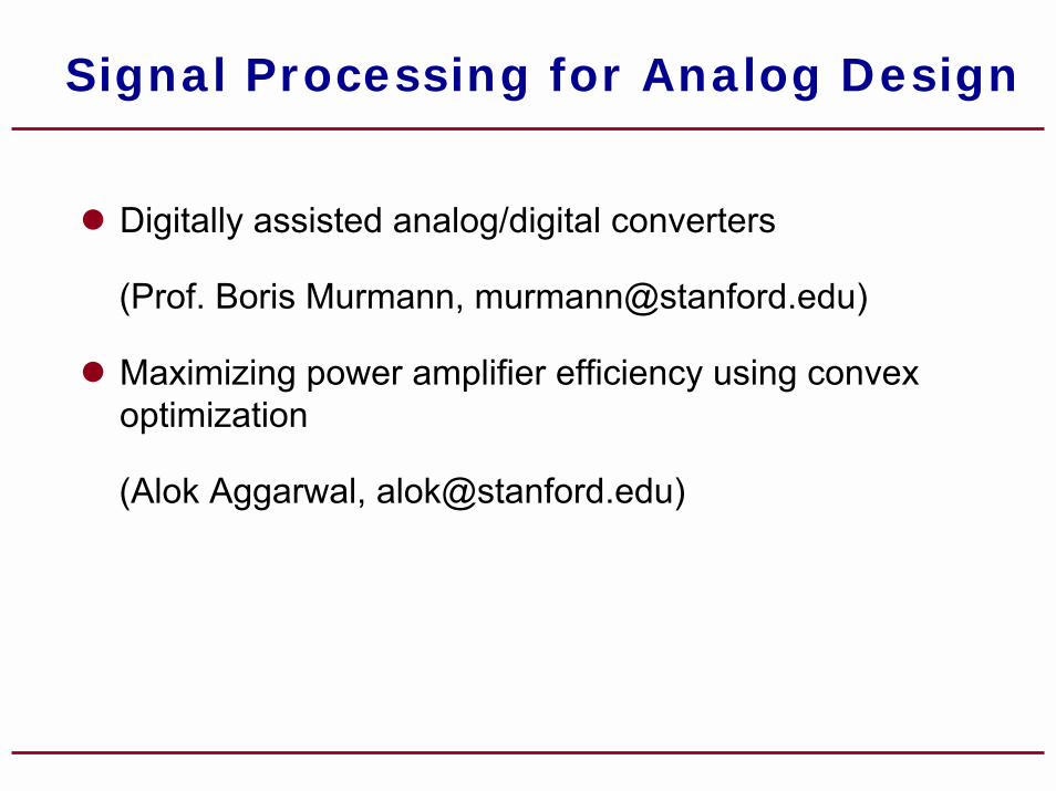
Signal Processing for Analog Design
! Digitally assisted analog/digital converters
(Prof. Boris Murmann, [email protected])
! Maximizing power amplifier efficiency using convex optimization
(Alok Aggarwal, [email protected])
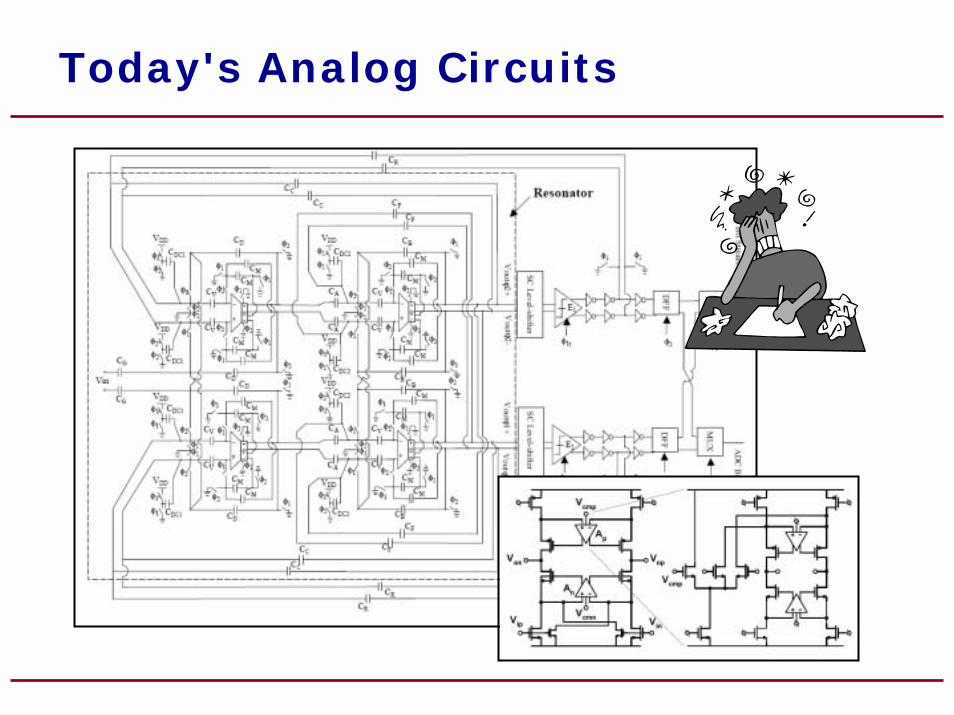
Today's Analog Circuits
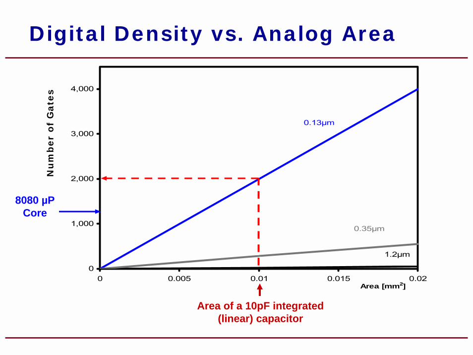
Digital Density vs. Analog Area
0
1,000
2,000
3,000
4,000
0 0.005 0.01 0.015 0.02Area [mm2]
0.13µm
1.2µm
0.35µm
8080 µP Core
Nu
mb
er
of
Gate
s
Area of a 10pF integrated (linear) capacitor
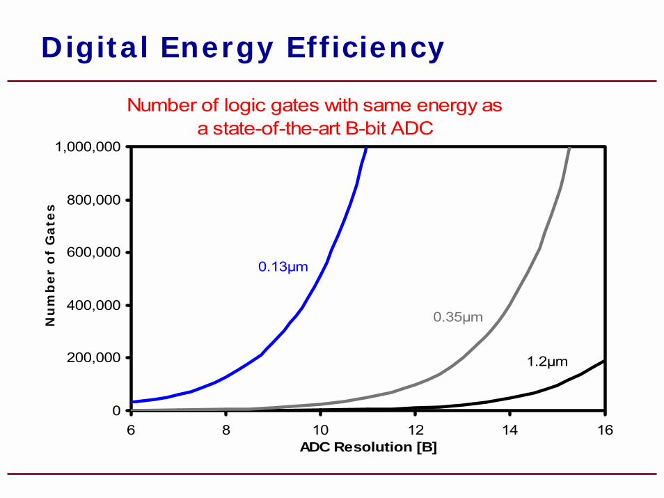
Digital Energy Efficiency
Number of logic gates with same energy as a state-of-the-art B-bit ADC
0
200,000
400,000
600,000
800,000
1,000,000
6 8 10 12 14 16ADC Resolution [B]
0.13µm
1.2µm
0.35µmNu
mb
er
of
Gate
s
Observations
! It is not new to realize that digital signal processing is superior to analog
! What's new is the relative size of the gap between digital and analog capabilities, mostly due to advancements of last 10 years
! Necessary paradigm shiftToday: "Let's use some logic gates to correct/calibrate analog circuits"Future: "How many analog transistors dowe really need?"
! How can we use digital logic more aggressively to "assist" analog functions, such as ADCs and PAs?
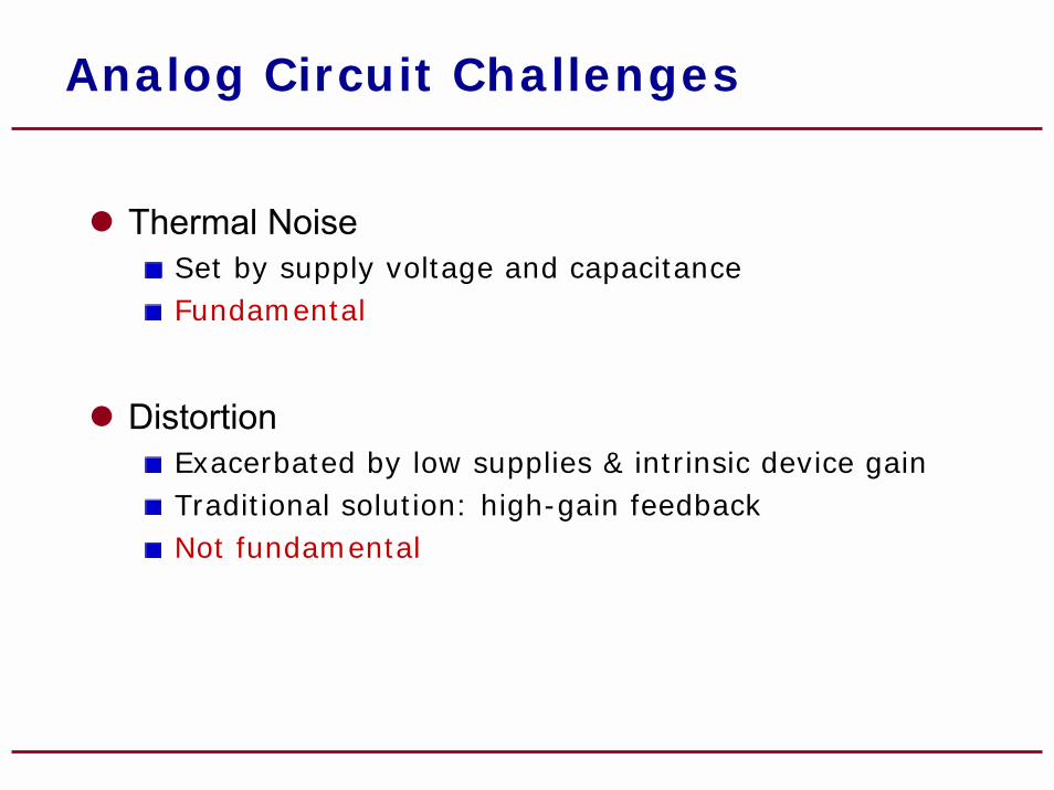
Analog Circuit Challenges
! Thermal NoiseSet by supply voltage and capacitanceFundamental
! DistortionExacerbated by low supplies & intrinsic device gainTraditional solution: high-gain feedbackNot fundamental
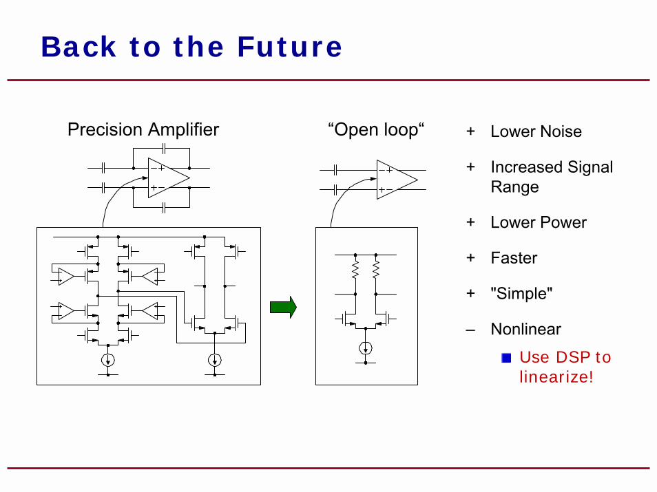
Back to the Future
+ Lower Noise
+ Increased Signal Range
+ Lower Power
+ Faster
+ "Simple"
� Nonlinear
Use DSP to linearize!
�Open loop�Precision Amplifier
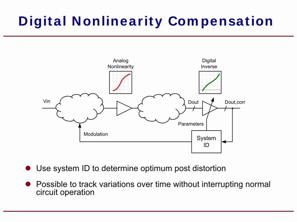
Digital Nonlinearity Compensation
SystemID
AnalogNonlinearity
DigitalInverse
Modulation
Dout,corrVin Dout
Parameters
! Use system ID to determine optimum post distortion
! Possible to track variations over time without interrupting normal circuit operation
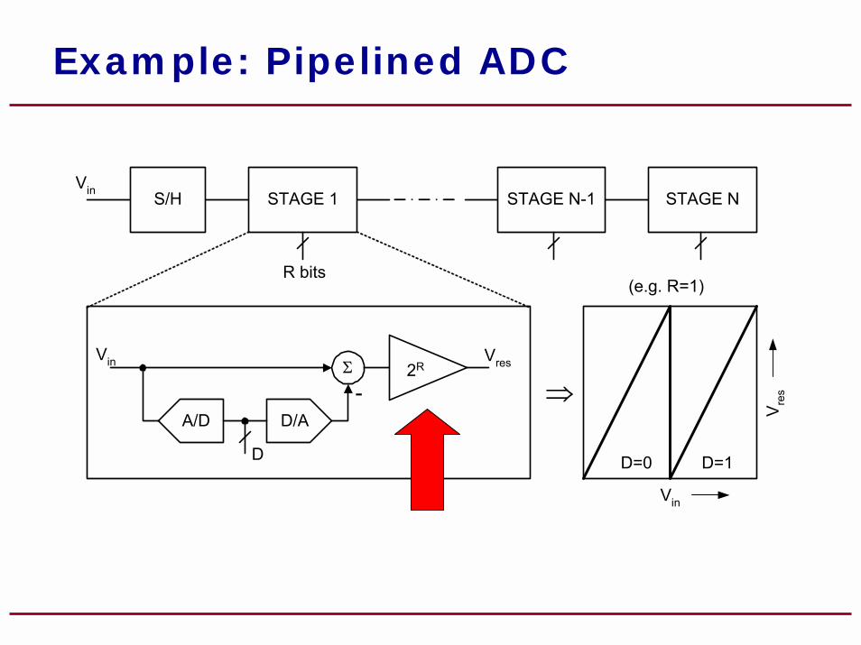
Example: Pipelined ADC
Σ
A/D D/A-
D
VresVin
STAGE 1 STAGE N-1 STAGE NS/H
R bits
Vin
2R
D=0 D=1
⇒
V
Vin
(e.g. R=1)
res
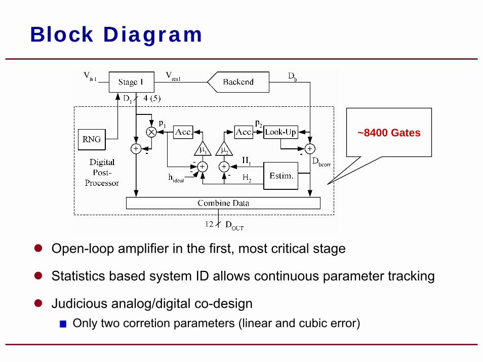
Block Diagram
~8400 Gates
! Open-loop amplifier in the first, most critical stage
! Statistics based system ID allows continuous parameter tracking
! Judicious analog/digital co-designOnly two corretion parameters (linear and cubic error)
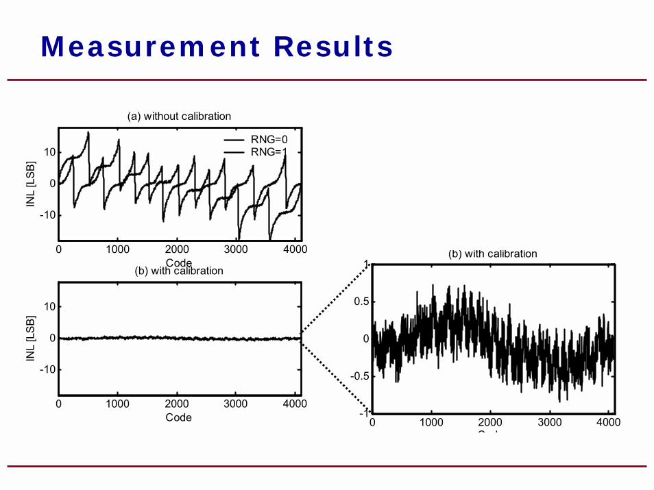
Measurement Results
0 1000 2000 3000 4000-1
-0.5
0
0.5
1(b) with calibration0 1000 2000 3000 4000
-10
0
10
(a) without calibration
Code
INL
[LSB
]
RNG=0RNG=1
0 1000 2000 3000 4000
-10
0
10
(b) with calibration
Code
INL
[LS
B]
C d
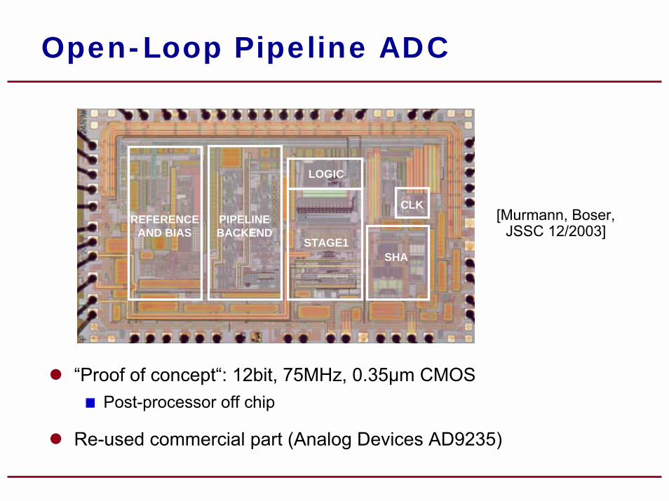
Open-Loop Pipeline ADC
REFERENCEAND BIAS
PIPELINEBACKEND
STAGE1SHA
CLK
LOGIC
[Murmann, Boser, JSSC 12/2003]
! �Proof of concept�: 12bit, 75MHz, 0.35µm CMOSPost-processor off chip
! Re-used commercial part (Analog Devices AD9235)
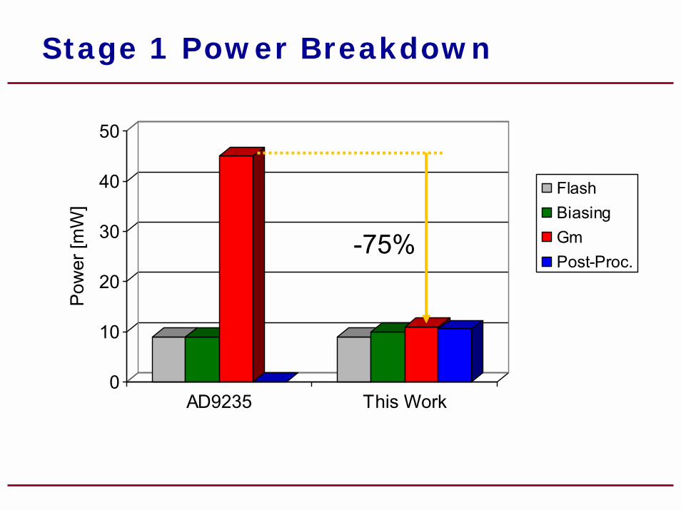
Stage 1 Power Breakdown
0
10
20
30
40
50
Pow
er [m
W]
AD9235 This Work
FlashBiasingGmPost-Proc.
-75%
The Next Steps
! Work in progress at Berkeley: Optimized deep sub-µm ADC (0.13µm)
Multi-stage calibration, hybrid voltage/current modeAggressive design to push speed, lower powerExpect to demonstrate 12b, 200MS/s, 200mWPower 4x below state-of-the art
! Various CAD projects at StanfordPipelined ADC with incomplete settling compensationMaximum entropy ADC arrays with adjustable DRADC for OFDM systems…
Summary - Digitially Assisted ADCs
! Simplified analog circuits are key to improving power efficiency in A/D
Power savings of better than one order of magnitude seem possible
! Other benefits of simplistic analog designsIntroduces redundancy, e.g. for yield enhancement
Creates adjustable, massively parallel arrays in small area
! Inherently self-calibrating, potentially self-repairingSimplifies testing
Ideal for remote, maintenance free operation, e.g. in remote sensing networks
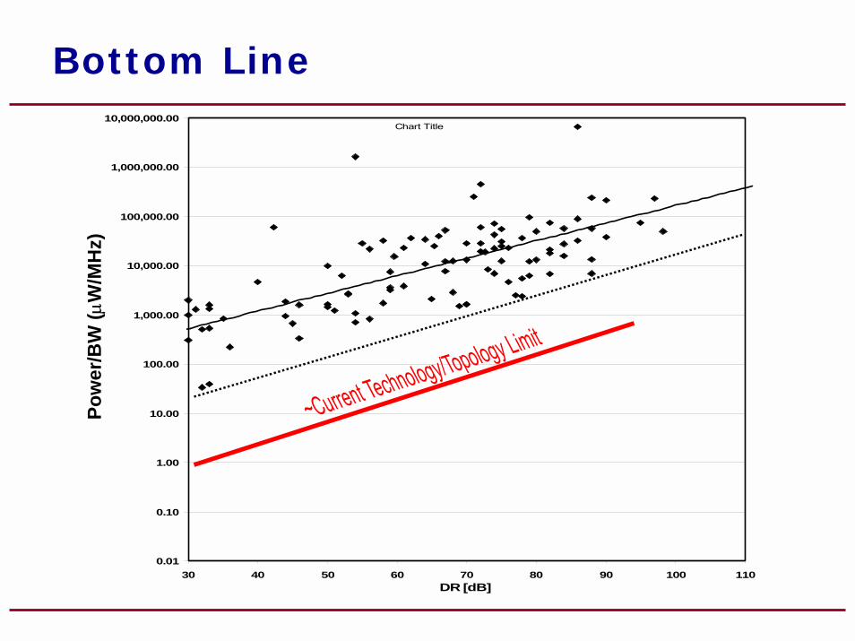
Bottom LineChart Title
0.01
0.10
1.00
10.00
100.00
1,000.00
10,000.00
100,000.00
1,000,000.00
10,000,000.00
30 40 50 60 70 80 90 100 110DR [dB]
Pow
er/B
W (µ
W/M
Hz)
Digitally Assisted PA Design
! Transmitter power efficiency is limited byHigh peak-to-average power ratio (PAR)
Power amplifier (PA) non-linearity
! Linear PA design is increasingly difficult
! Digital circuit capabilities grow exponentially1 GOPS/mW, 1 GOPS/mm2 in 0.13 µm CMOS
! How to achieve maximum power efficiency?
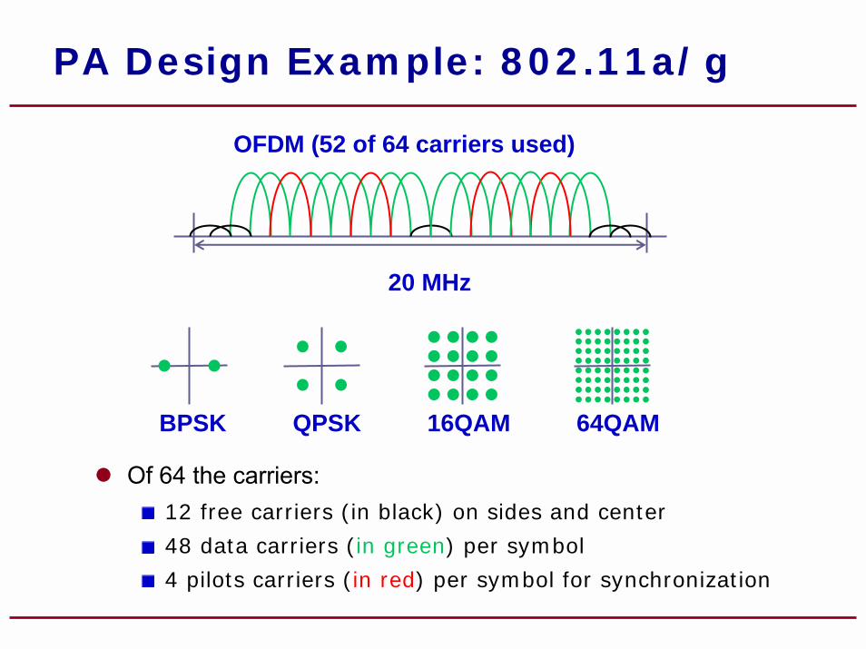
PA Design Example: 802.11a/g
OFDM (52 of 64 carriers used)
20 MHz
BPSK QPSK 16QAM 64QAM
! Of 64 the carriers:12 free carriers (in black) on sides and center
48 data carriers (in green) per symbol
4 pilots carriers (in red) per symbol for synchronization
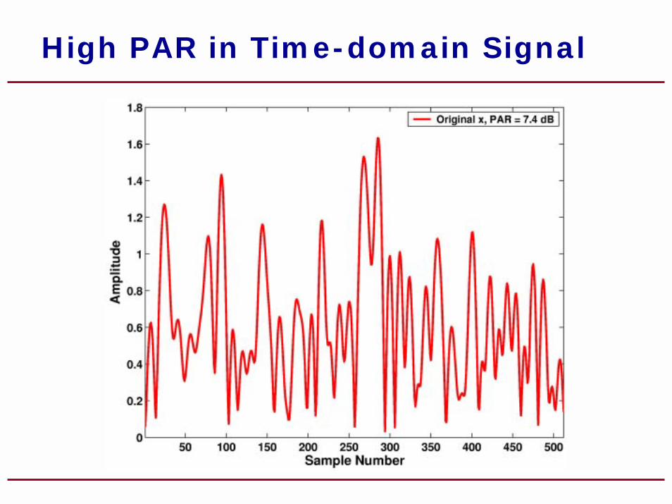
High PAR in Time-domain Signal
Peak-to-average Power Ratio
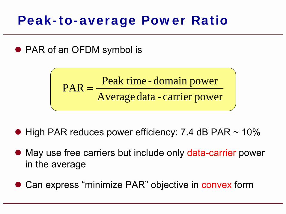
! PAR of an OFDM symbol is
! High PAR reduces power efficiency: 7.4 dB PAR ~ 10%
! May use free carriers but include only data-carrier power in the average
! Can express �minimize PAR� objective in convex form
powercarrier -data Averagepowerdomain -Peak timePAR =
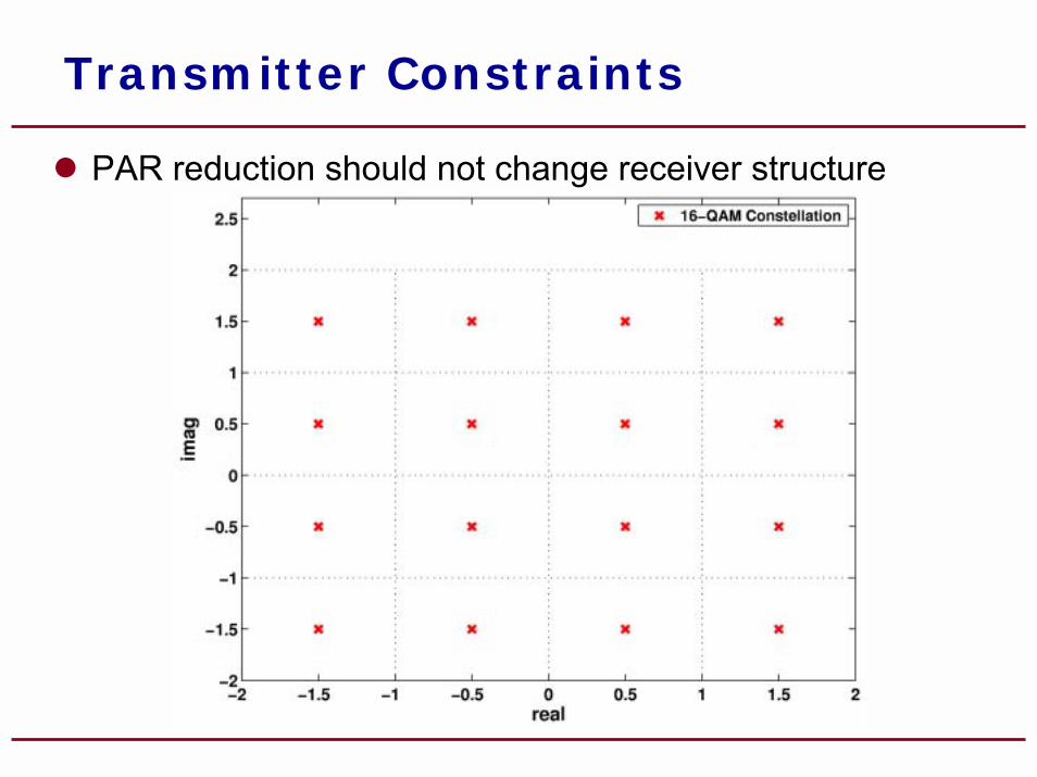
Transmitter Constraints
! PAR reduction should not change receiver structure
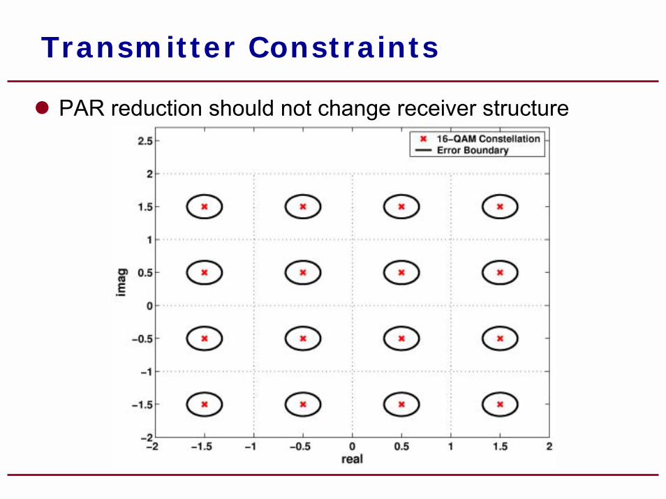
Transmitter Constraints
! PAR reduction should not change receiver structure
Transmitter Constraints
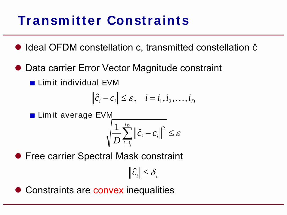
! Ideal OFDM constellation c, transmitted constellation ĉ
! Data carrier Error Vector Magnitude constraintLimit individual EVM
Limit average EVM
! Free carrier Spectral Mask constraint
! Constraints are convex inequalities
ε≤−∑=
D
i
i
iiii cc
D2ˆ1
Dii iiiicc ,,,,ˆ 21 K=≤− ε
iic δ≤ˆ
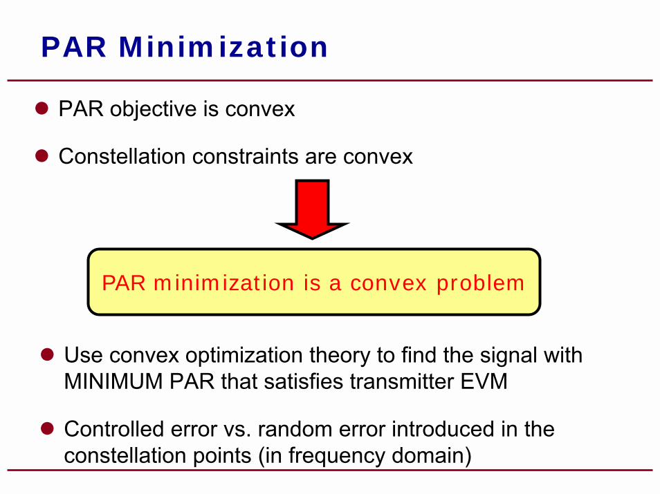
PAR Minimization
! PAR objective is convex
! Constellation constraints are convex
PAR minimization is a convex problem
! Use convex optimization theory to find the signal with MINIMUM PAR that satisfies transmitter EVM
! Controlled error vs. random error introduced in the constellation points (in frequency domain)
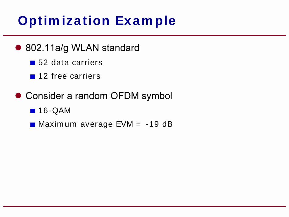
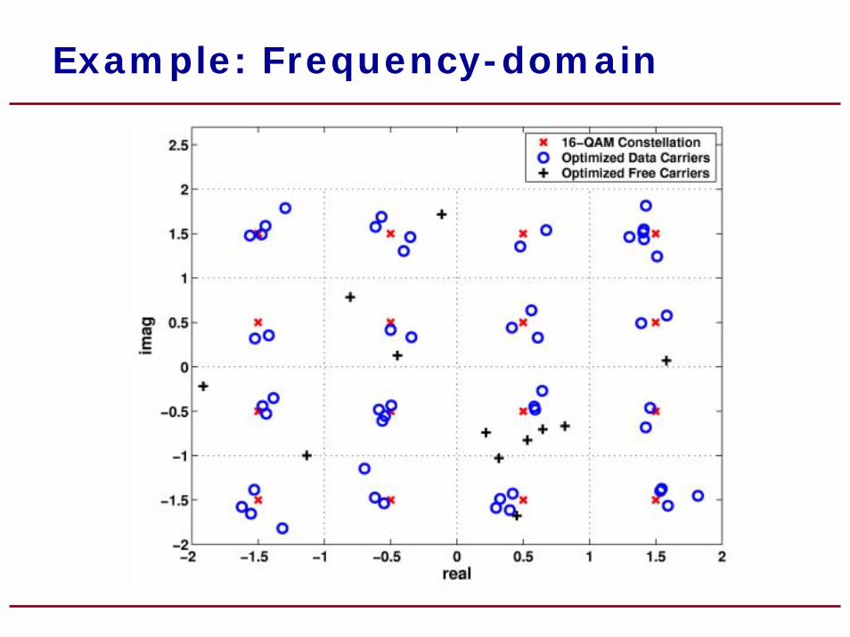
Optimization Example
! 802.11a/g WLAN standard52 data carriers
12 free carriers
! Consider a random OFDM symbol16-QAM
Maximum average EVM = -19 dB
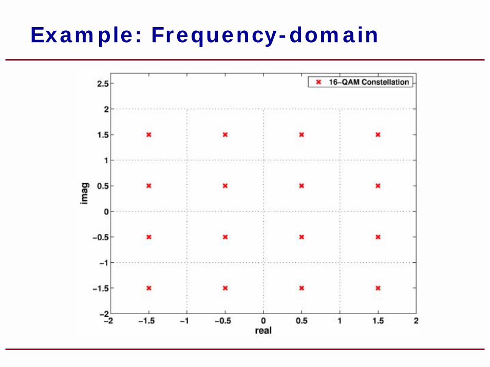
Example: Frequency-domain
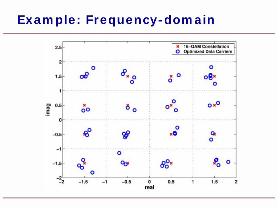
Example: Frequency-domain
Example: Frequency-domain
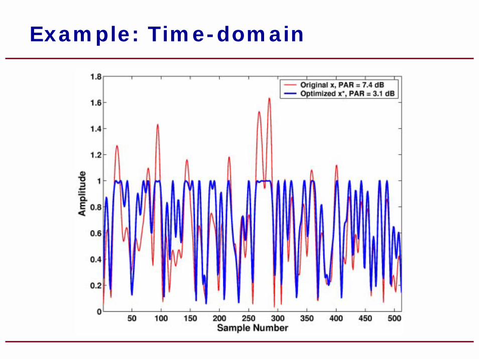
Example: Time-domain
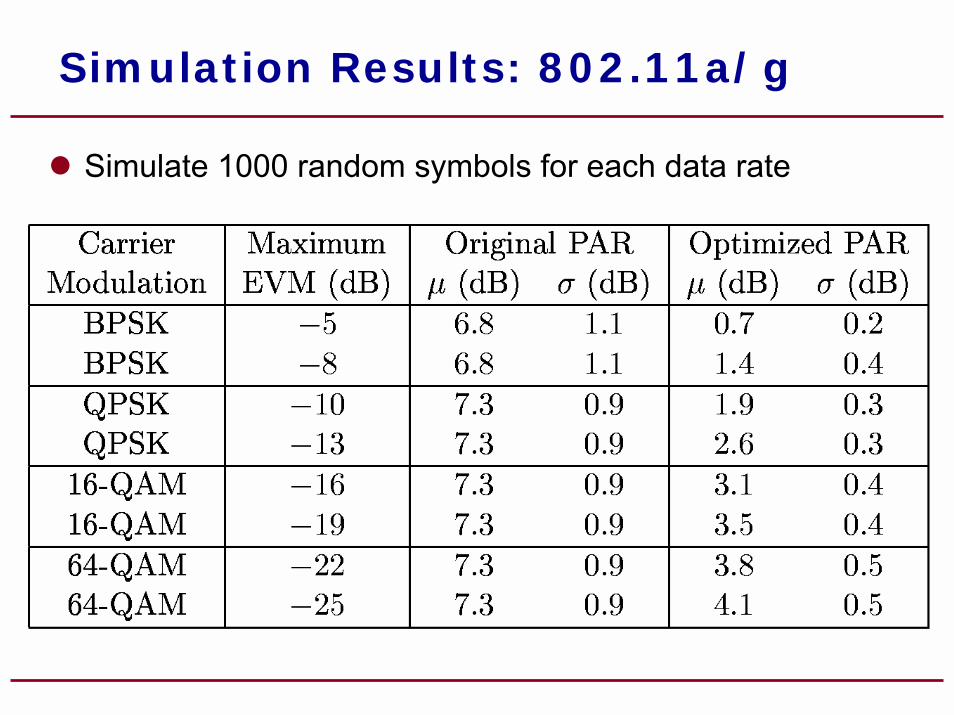
Simulation Results: 802.11a/g
! Simulate 1000 random symbols for each data rate
Convex Optimized PA
! Achieves globally minimum PAR in OFDM signals
! Delivers maximum power efficiency
! Establishes performance limits for analyzing existing PAR reduction methods
! Is feasible for real-time implementation using modern CMOS technology
Conclusion
! With the availability of energy efficient, dense and cheap digital technology, we must challenge basic analog design techniques
! Digital assistance in analog circuit design
Digital compensation and correction
Real-time calibration
! Key to success: Interdisciplinary approach
Device modeling
Analog circuit design
DSP algorithms
! Lots of room for performance growth, independent of scaling roadmap!
Digital Performance
1.0E+00
1.0E+01
1.0E+02
1.0E+03
1.0E+04
1985 1990 1995 2000 2005
Rel
ativ
e Pe
rfor
man
ce
Delay/ft (2x/5years)
µP fclk (2x/2.3 years)
µP MIPS (2x/1.5years)
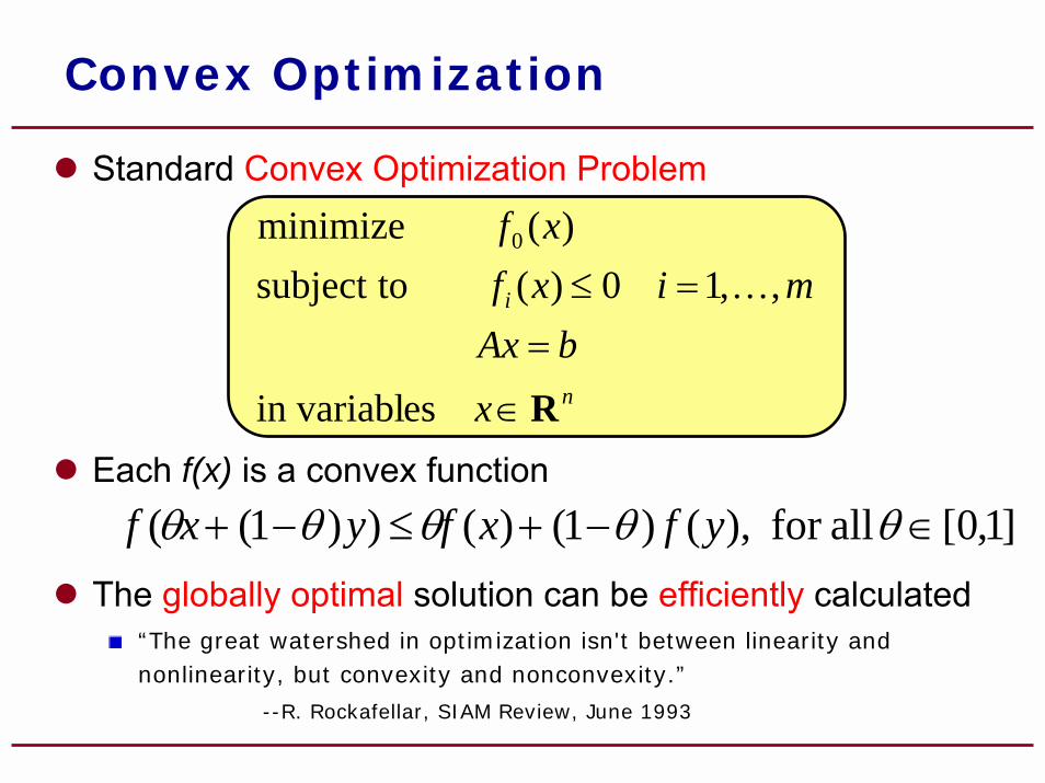
Convex Optimization
! Standard Convex Optimization Problem
! Each f(x) is a convex function
! The globally optimal solution can be efficiently calculated“The great watershed in optimization isn't between linearity andnonlinearity, but convexity and nonconvexity.”
--R. Rockafellar, SIAM Review, June 1993
n
i
xbAx
mixfxf
R∈
==≤
esin variabl
,,10)(tosubject)(minimize 0
K
]1,0[allfor),()1()())1(( ∈−+≤−+ θθθθθ yfxfyxf
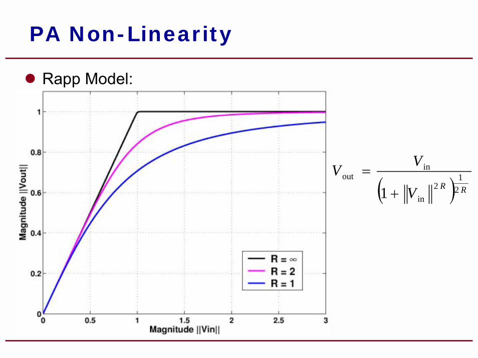
PA Non-Linearity
! Rapp Model:
( ) RRV
VV21
2in
inout
1 +=
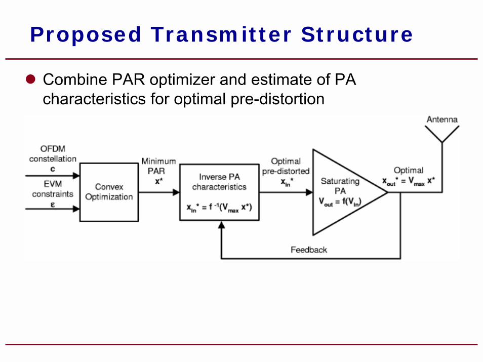
Proposed Transmitter Structure
! Combine PAR optimizer and estimate of PA characteristics for optimal pre-distortion
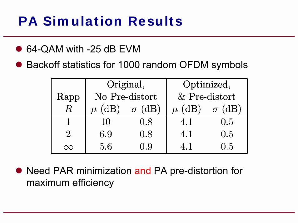
PA Simulation Results
! 64-QAM with -25 dB EVM! Backoff statistics for 1000 random OFDM symbols
! Need PAR minimization and PA pre-distortion for maximum efficiency