Embed Size (px)
Citation preview

APPLICATION NOTE
Digital Video Decoder/Encoder Module System
AN96055

Abstract
Digital Video Decoder/Encoder Module System
Philips Semiconductors
Application NoteAN96055
2
Philips Electronics N.V. 1997
All rights are reserved. Reproduction in whole or in part is prohibited without the prior written consent of the copy-right owner.
The information presented in this document does not form part of any quotation or contract, is believed to beaccurate and reliable and may be changed without notice. No liability will be accepted by the publisher for anyconsequence of its use. Publication thereof does not convey nor imply any license under patent- or other indus-trial or intellectual property rights.
This application note is intended to provide application support for Philips´ Digital Video Decoders and Encoders. It contains a description of various evaluation boards as well as I²C-bus programming of the ICs.
The Digital Video Decoder converts an analog video input signal into a digital output signal. This signal can be processed by a wide range of applications and fed to the Digital Video Encoder, which delivers analog video sig-nals to TV receivers or video cassette recorders.
This note gives a detailed description of the schematics and some hints how to design the PCB (Printed Circuit Board) with mixed analogue and digital signal processing.

Keywords
Philips Semiconductors
Author:
Digital Video Decoder/Encoder Module System Application NoteAN96055
3
APPLICATION NOTE
Digital Video Decoder/Encoder Module System
Thomas GrubeProduct Concept & Application Laboratory Hamburg,
Germany
SAA7110(A) / SAA7111(A), OCF / VIPDigital Video Decoder
SAA7124/25 SAA7182/83
SAA7182A/83ADigital Video Encoder (DENC)
I²C BusMultiMedia
Date: 31th May 1996
AN96055

Summary
Digital Video Decoder/Encoder Module System
Philips Semiconductors
Application NoteAN96055
4
This application note is intended to provide application support for Philips´ Digital Video Decoders and Encoders. It contains a description of various evaluation boards as well as I²C-bus programming of the ICs.
The Digital Video Decoder converts an analog video input signal into a digital output signal. This signal can be processed by a wide range of applications and fed to the Digital Video Encoder, which delivers analog video sig-nals to TV receivers or video cassette recorders.
This note gives a detailed description of the schematics and some hints how to design the PCB (Printed Circuit Board) with mixed analogue and digital signal processing.

Digital Video Decoder/Encoder Module System
Philips Semiconductors
5
Application NoteAN96055
CONTENTS
1. Introduction . . . . . . . . . . . . . . . . . . . . . . . . . . . . . . . . . . . . . . . . . . . . . . . . . 7
2. Digital Video Decoder Module DECMOD01 . . . . . . . . . . . . . . . . . . . . . . . . . . . . . . . . 7
3. Digital Video Encoder Module ENCMOD02 . . . . . . . . . . . . . . . . . . . . . . . . . . . . . . . . 9
4. I²C-bus EEPROM on DECMOD01 and ENCMOD02 . . . . . . . . . . . . . . . . . . . . . . . . . . . 12
5. Module System Connectors . . . . . . . . . . . . . . . . . . . . . . . . . . . . . . . . . . . . . . . 13
6. Desktop Video Evaluation Board DTV7183 . . . . . . . . . . . . . . . . . . . . . . . . . . . . . . . 14
7. Digital Video Encoder Board DENC2 . . . . . . . . . . . . . . . . . . . . . . . . . . . . . . . . . . . 14
8. Desktop Video Evaluation Board DTV4 . . . . . . . . . . . . . . . . . . . . . . . . . . . . . . . . . 15
9. Tips for a PCB layout with analog and digital signal processing . . . . . . . . . . . . . . . . . . . 16
10. Programming tables for SAA7111, SAA7182/83 and SAA7184/85B/88A . . . . . . . . . . . . . . . . 17
11. Programming tables for SAA7110(A), SAA7187 and SAA 7124/25 . . . . . . . . . . . . . . . . . . . 18
12. Appendix: Schematics and Layout . . . . . . . . . . . . . . . . . . . . . . . . . . . . . . . . . . . . 19
12.1 Schematics . . . . . . . . . . . . . . . . . . . . . . . . . . . . . . . . . . . . . . . . . . . . . 2012.1.1 Power Supply, EEPROM and Connectors of DECMOD01 . . . . . . . . . . . . . . . 2012.1.2 Digital Video Decoder of DECMOD01 . . . . . . . . . . . . . . . . . . . . . . . . . 2112.1.3 Top sheet of ENCMOD02. . . . . . . . . . . . . . . . . . . . . . . . . . . . . . . . 2212.1.4 Digital Video Encoder of ENCMOD02 . . . . . . . . . . . . . . . . . . . . . . . . . 2312.1.5 Additional IC packages for ENCMOD02 . . . . . . . . . . . . . . . . . . . . . . . . 2412.1.6 Inputs of ENCMOD02 . . . . . . . . . . . . . . . . . . . . . . . . . . . . . . . . . . 2512.1.7 Outputs of ENCMOD02 . . . . . . . . . . . . . . . . . . . . . . . . . . . . . . . . . 2612.1.8 Power Supply and EEPROM of ENCMOD02 . . . . . . . . . . . . . . . . . . . . . . 27
12.2 Layout . . . . . . . . . . . . . . . . . . . . . . . . . . . . . . . . . . . . . . . . . . . . . . . 2812.2.1 Top placement of DECMOD01 . . . . . . . . . . . . . . . . . . . . . . . . . . . . . 2812.2.2 Routing of top layer of DECMOD01. . . . . . . . . . . . . . . . . . . . . . . . . . . 2912.2.3 Bottom placement of DECMOD01 . . . . . . . . . . . . . . . . . . . . . . . . . . . 3012.2.4 Routing of bottom layer of DECMOD01. . . . . . . . . . . . . . . . . . . . . . . . . 3112.2.5 Routing of ground plane layer of DECMOD01 . . . . . . . . . . . . . . . . . . . . . 3212.2.6 Routing of power supply layer of DECMOD01 . . . . . . . . . . . . . . . . . . . . . 3312.2.7 Top placement of ENCMOD02 . . . . . . . . . . . . . . . . . . . . . . . . . . . . . 3412.2.8 Routing of top layer of ENCMOD02. . . . . . . . . . . . . . . . . . . . . . . . . . . 3512.2.9 Routing of bottom layer of ENCMOD02. . . . . . . . . . . . . . . . . . . . . . . . . 3612.2.10 Routing of ground plane layer of ENCMOD02 . . . . . . . . . . . . . . . . . . . . . 3712.2.11 Routing of power supply layer of ENCMOD02 . . . . . . . . . . . . . . . . . . . . . 38

6
Digital Video Decoder/Encoder Module System
Philips Semiconductors
Application NoteAN96055

Digital Video Decoder/Encoder Module System
Philips Semiconductors
7
Application NoteAN96055
1. IntroductionThe Digital Video Decoder/Encoder Modules provide the basis to evaluate various Philips digital video decoders and encoders and give the opportunity to simply insert the modules into customized applications and systems.
On the following pages the schematics of the Digital Video Decoder Module DECMOD01 and Digital Video Encoder Module ENCMOD02 are shown. Both modules can be operated in stand alone operation (intercon-nected directly) as well as extension to other systems like PCI-bridges, MPEG decoders or Video input/output systems.
Each module has a socket for an I²C-bus EEPROM (e.g. PCF8582, PCF8594, PCF8598, X24164) in order to store data for initialization and for simple control functionality operated by a (future) microcontoller module. Soft-ware for IBM compatible personal computers enables access to all features and settings of the devices. It han-dles the I²C-bus via a printer port adapter.
This modular concept was designed to combine different video decoders with various video encoders. Each module can be configured for several devices and packages without the necessity of having a new PCB. This could be achieved by using multiple footprints for one IC and some configurational parts. For interfacing a 26-pin and a 16-pin flat ribbon cable connector is used. The 26-pin YUV-Feature Connector is used for the signal path while the other one is used for power supply and I²C-bus.
2. Digital Video Decoder Module DECMOD01The digital decoder module DECMOD01 contains the decoder types SAA7110(A) or SAA7111(A) and allows the assembly of PLCC68 and LQFP64 packages.
The module has two RCA jacks for CVBS input signals and a DIN connector for S-Video input. For the 3.3V device SAA7111A the input termination is constructed as resistor divider (27R + 47R) to meet the input voltage range of approx. 0.7Vpp. For all other devices the series resistor is 0R and the termination 75R. The coupling capacitors are 22 nF for SAA7111A and 10 nF for all other. As crystal a 3rd order type is used for SAA7110(A) and SAA7111 (see data sheets for details on crystal parameters).
Fig.1 Location of ICs, jumpers and connectors on the DECMOD01 PCB
LQFP64
PLCC68
DEC1.wmf
J3
J2
JP3
JP1
J1
T13 T14
T11 T12
T1 T2 T3
JP2
J4
J5
J6
U1
U5
JP7
JP8
JP6
JP5
JP4
U4
U3 U2
8
Digital Video Decoder/Encoder Module System
Philips Semiconductors
Application NoteAN96055
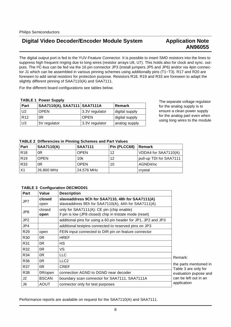
The digital output port is fed to the YUV-Feature Connector. It is possible to insert SMD resistors into the lines to suppress high frequent ringing due to long wires (resistor arrays U6, U7). This holds also for clock and sync. out-puts. The I²C-bus can be fed via the 16 pin connector JP3 (install jumpers JP5 and JP6) and/or via 4pin connec-tor J1 which can be assembled in various pinning schemes using additionally pins (T1~T3). R17 and R20 are foreseen to add serial resistors for protection purpose. Resistors R18, R19 and R33 are foreseen to adapt the slightly different pinning of SAA7110(A) and SAA7111.
For the different board configurations see tables below.
Performance reports are available on request for the SAA7110(A) and SAA7111.
TABLE 2 Differencies in Pinning Schemes and Part ValuesPart SAA7110(A) SAA7111 Pin (PLCC68) Remark
R18 0R OPEN 12 VDDA4 for SAA7110(A)
R19 OPEN 10k 12 pull-up TDI for SAA7111
R33 0R OPEN 10 AGND4/nc
X1 26.800 MHz 24.576 MHz crystal
TABLE 1 Power SupplyPart SAA7110(A), SAA7111 SAA7111A Remark
U2 OPEN 3.3V regulator digital supply
R12 0R OPEN digital supply
U3 5V regulator 3.3V regulator analog supply
The separate voltage regulator for the analog supply is to ensure a clean power supply for the analog part even when using long wires to the module
TABLE 3 Configuration DECMOD01Part Value Description
JP7closedopen
slaveaddress 9Ch for SAA71 10, 48h for SAA7 111(A)slaveaddress 9Eh for SAA7110(A), 4Ah for SAA7111(A)
JP8closedopen
only for SAA7111(A): CE pin (chip enable)if pin is low (JP8 closed) chip in tristate mode (reset)
JP2 additional pins for using a 60 pin header for JP1, JP2 and JP3
JP4 additional testpins connected to reserved pins on JP3
R29 open FEIN input connected to DIR pin on feature connector
R30 0R HREF
R31 0R HS
R32 0R VS
R34 0R LLC
R36 0R LLC2
R37 0R CREF
R38 0R/open connection AGND to DGND near decoder
J2 BSCAN boundary scan connector for SAA7111, SAA7111A
J6 AOUT connector only for test purposes
Remark:
the parts mentioned in Table 3 are only for evaluation pupose and can be left out in an application

Digital Video Decoder/Encoder Module System
Philips Semiconductors
9
Application NoteAN96055
3. Digital Video Encoder Module ENCMOD02The digital encoder module ENCMOD02 contains the encoder types SAA7182/83, SAA7182A/83A or SAA7124/25 and allows the assembly of PLCC84, QFP80 and LQFP64 package. The digital data is fed via the 26-pin YUV Feature Connector, power and I²C-bus via 16-pin header. Depending on the assembled IC the data can be in CCIR 656 format (D1) or 16-bit YUV (SAA7182/83/82A/83A only). The outputs of the D/A converters are fed through analog postfilters to the connectors. Depending on the signal type the serial resistor varies. Therefor the filters are assigned to the connectors and the signals out of the D/A converters are routed via jumpers to adapt the different output modes of the SAA7124/25 (JP16, JP17, JP18; see tables below).
On connector J1 On-Screen-Display (OSD) signals can be fed to the encoders SAA7182/83/82A/83A. The SAA7182A/83A also features RGB input pins which are connected to J3 via optional resistor dividers to adapt the input voltage range.
The clock and synchronization signals can be fed to the encoder via jumper (JP10, JP11, JP14, JP15) when operating the slave mode (pin CDIR high; JP13 open). Using the encoder as clock master (pin CDIR low; JP13 closed) LLC and CREF are outputs. The pins RCV1 and RCV2 can be configured to outputs via I²C-bus setting (see I²C-bus register 6Bh in datasheets) to provide horizontal and vertical synchronization signals.
Fig.2 Location of ICs, jumpers and connectors on the ENCMOD02 PCB
LQFP64
PLCC84
J7
J4
J5
J6
ENC1.wmf
JP3
JP1
JP2
J3
JP6
JP7
JP5
T9 T10
T11 T12
U1
U5
JP12
JP4
U4
U2
JP14
U3
QFP80
U6
JP8
JP9
JP10
JP11
JP15
JP13
JP16
JP17
JP18
JP20
JP19
J2T1 T2 T3J1

10
Digital Video Decoder/Encoder Module System
Philips Semiconductors
Application NoteAN96055
JP16
JP17
JP18
JP16
JP17
JP18
Y C
R (or Cr)
G (or Y)
CVBSB (or Cb)
CVBS
C
CVBS
Y
RGB (or YUV) mode S-Video mode(SAA7124/25 only)
The jumper configuration for the S-Video mode is only for the SAA7124/25. This mode can be configured via I²C-bus. The four D/A converters deliver Y,C and two times CVBS.
The configuration for RGB mode can be used for all devices. In this configuration the four D/A converters of the SAA7124/25 can deliver either CVBS and RGB signals or CVBS and analog YUV signals (Y and C is not available). Additionally the SAA7182/83/82A/83A delivers S-Video output signals (Y and C).
TABLE 4 Power Supply
PartSAA7124/25, SAA7182/83 SAA7182A/83A Remark
U2 OPEN 3.3V regulator digital supply
R12 0R 0R digital supply
R14 0R OPEN digital supply
U3 5V regulator 3.3V regulator analog supply
The separate voltage regulator for the analog supply is to ensure a clean power supply for the analog part even when using long wires to the module

Digital Video Decoder/Encoder Module System
Philips Semiconductors
11
Application NoteAN96055
Remark:
the parts mentionedin Table 5 are only forevaluation pupose and can be left out in an application
TABLE 5 Configuration ENCMOD02Part Value Description
JP12closedopen
slaveaddress 88hslaveaddress 8Ch
JP13closedopen
CDIR pin (clock direction): pins LLC and CREF are outputs and the internal oszillator will be used if CDIR is low (JP13 closed)
JP2 additional pins for using a 60 pin header for JP1, JP2 and JP3
JP4 additional testpins connected to reserved pins on JP3
JP5JP6JP7
additional pins for using reverse connectors
R33 open termination CREF
R34 open termination LLC
R35 0R connection AGND to DGND near encoder
JP14 jumper CREF
JP15 jumper LLC
JP11 HS/HREF to/from RCV2
JP10 VS to/from RCV1
J2 OSD OSD connector for SAA7182/83(A)
J3 RGBinRGB input connector for SAA7183AR15,16,17,18,23,24,26,27 used to adapt input voltage range
T5 RESN testpin (active low reset input)
T7 TTXRQ testpin (output signal for teletext request)
T8 TTX testpin (input signal for teletext data)
R25/R28 0R I²C-bus serial resisitors for protection
JP161-22-3
S-Video-Mode (SAA7124/25 only)RGB-Mode
JP171-2, 3-4, 5-62-3, 4-5
RGB-ModeS-Video-Mode (SAA7124/25 only)
JP181-2, 3-42-3
RGB-ModeS-Video-Mode (SAA7124/25 only)
JP191-22-3
HSYNC to J7 pin13 (VGA connector)CVBS to J7 pin14 (VGA connector)
JP20 closed VSYNC to J7 pin14 (VGA connector)

12
Digital Video Decoder/Encoder Module System
Philips Semiconductors
Application NoteAN96055
4. I²C-bus EEPROM on DECMOD01 and ENCMOD02The IC U1 on each module can be assembled with different IC types depending on the desired memory size. Additionally the I²C-bus device address can be adapted by soldering corresponding SMD resistors which is described in the tables below.
TABLE 6 Configuration of I²C-bus EEPROMsIC type Size Pin 1 Pin 2 Pin 3 Pin 7 Address Range
PCF8582x-2 256 bytes
A0:“0”“1”“0”“1”“0”“1”“0”“1”
A1:“0”“0”“1”“1”“0”“0”“1”“1”
A2:“0”“0”“0”“0”“1”“1”“1”“1”
PTC
A0h orA2h orA4h orA6h orA8h orAAh orACh orAEh
PCF8594x-2 512 bytes WP
A1:“0”“1”“0”“1”
A2:“0”“0”“1”“1”
PTCA0h and A2h orA4h and A6h orA8h and AAh orACh and AhE
PCF8598x-2 1024 bytes WP n.c.A2:“0”“1”
PTC A0h, A2h, A4h and A6h orA8h, AAh, ACh and AEh
X24164 2048 bytes
S0:“0”“1”“0”“1”“0”“1”“0”“1”
S1:“1”“1”“0”“0”“1”“1”“0”“0”
S2:“0”“0”“0”“0”“1”“1”“1”“1”
TEST
80h, 82h, 84h, 86h, 88h, 8Ah, 8Ch and 8Eh or90h, 92h, 94h, 96h, 98h, 9Ah, 9Ch and 9Eh orA0h, A2h, A4h, A6h, A8h, AAh, ACh and AEh orB0h, B2h, B4h, B6h, B8h, BAh, BCh and BEh orC0h, C2h, C4h, C6h, C8h, CAh, CCh and CEh orD0h, D2h, D4h, D6h, D8h, DAh, DCh and DEh orE0h, E2h, E4h, E6h, E8h, EAh, ECh and EEh orF0h, F2h, F4h, F6h, F8h, FAh, FCh and FEh
TABLE 7 Board Configuration for I²C-bus EEPROMSPin “0” “1” Remark
PTC or TESTR4: OPENR8: 0R
R4: 0RR8: OPEN
Leave pin PTC open; apply “0” to pin TEST
A2 or S2R5: OPENR9: 0R
R5: 0RR9: OPEN
A1 or S1R6: OPENR10: 0R
R6: 0RR10: OPEN
pin S1 (X24164) is inverted internally
WP, A0 or S0R7: OPENR11: 0R
R7: 0RR11: OPEN
WP: “1” --> write protect of upper 256[512] bytes“0” --> write enabled (only PCF8594[PCF8598])

Digital Video Decoder/Encoder Module System
Philips Semiconductors
13
Application NoteAN96055
5. Module System ConnectorsThe YUV connector (feature connector) provides access to the digital YUV data input coming from a digital video decoder or from an MPEG video source supplied to a video encoder. Two YUV data formats are supported, 16-bit “decoder format” or 8-bit CCIR656 compatible (D1). The control lines are set either as inputs or outputs. The connector has the following pin assignment:
Pin 1, 3, 5, 7, 9, 11, 13, 15 UV0: UV7 digital UV dataPin 2, 4, 6, 8, 10, 12, 14, 16 Y0: Y7 digital Y data or digital CCIR656 dataPin 17 LLC digital clockPin 18 LLC2Pin 19 CREF, clock referencePin 20 HREF, optional horizontal reference (blanking)Pin 21 RTC, real time controlPin 22 HS, horizontal synchronisation pulsePin 23 digital groundPin 24 VS, vertical synchronisation pulsePin 25 DIRPin 26 digital ground
The 16-pin header for power supply and I²C-bus has the following pin assignment:
Pin 1 SCLPin 2 SDAPin 3, 4, 9, 10, 15, 16 reserved for future usePin 5, 6 digital power supply (5V)Pin 7, 8 digital groundlPin 11, 12 analog power supply (12V)Pin 13, 14 analog ground
On each module in addition (or as alternative) a 4 pin connector can be used for I²C-bus control:
Fig.3 I²C-bus connector pinnings
Note: always supply the I²C-bus with pull-up resistors, but avoid too high currents (see I²C-bus specification)On each module pull-up resistors can be added (R1 and R2), but preferably only one pull-up should bedone on the I²C-bus master IC.
I2C_CON6.wmf
I2C-NEW
SCLGND
1234 SDA
+5V
using 3 additional pins,one out of the three common used pin configurations can be stuffed
I2C-NEW
SCLGND
1234 SDA
+5V
SDASCLGND+5V
SDA+5V
GNDSCL
1234
I2C-OLD(Europe)
SDA+5V
GNDSCL 1
234
I2C(US)
SDA
+5VGNDSCL
T1
T2T3

14
Digital Video Decoder/Encoder Module System
Philips Semiconductors
Application NoteAN96055
6. Desktop Video Evaluation Board DTV7183SAA7110(A) or SAA7111; PLCC68 (Digital Video Decoder)SAA7185 or SAA7187 or SAA7188A or SAA7184/85B; PLCC68 (Digital Video Encoder)SAA7182/83; QFP80 (Digital Video Encoder); note: only samples for demo purposes in this package!
The DTV7183 Demonstration Board shows the features and the application of the digital video decoder and encoder families.
The board operates in stand alone mode as well as an extension board for other Desktop Video boards. It incor-porates the ICs of the digital encoder family SAA7185, SAA7187, SAA7188A and SAA7184/85B, the EURO-DENC SAA7182/SAA7183 and the video decoders SAA7110(A)/SAA7111. The digital datapath is connected to the YUV Feature Connector, which can be used as input or output.
The on-board microcontroller delivers different I²C-bus setups for easy demonstration.
The User Manual HSM/UM95003 gives a detailed description of the board, summarises the control software fea-tures and provides the schematics and the board layout.
Fig.4 Blockdiagram of the DTV7183 demonstration board
7. Digital Video Encoder Board DENC2 SAA7185 or SAA7187 or SAA7188A; PLCC68
The DENC2 Demonstration Board operates as a stand alone video pattern generator as well as an extension board for the other Desktop Video decoder boards. It incorporates the ICs of the digital encoder famliy SAA7185, SAA7187 and SAA7188A. The digital input data from the YUV Feature Connector is sent directly to the encoder and the processed analog video output signals are CVBS and S-Video.
The on-board microcontroller delivers eigth different I²C setups for easy demonstration.
The User Manual HVS/UM94008 gives a detailed description of the board, summarises the control software fea-tures and provides the schematics and the board layout.
DigitalColor
Decoder
SAA7110SAA7111
DigitalColor
Encoder
SAA7183
DigitalColor
Encoder
SAA7185SAA7187
SAA7188A
µ-Controller
7183FIG8.wmf
YUV FeatureConnector
Digital YUV bus
Analog Inputs(CVBS,S-Video)
Analog Outputs(CVBS,S-Video)
Analog Outputs(CVBS,S-Video,RGB)

Digital Video Decoder/Encoder Module System
Philips Semiconductors
15
Application NoteAN96055
Fig.5 Blockdiagram of the DENC2 board
8. Desktop Video Evaluation Board DTV4
The DTV4 evaluation board demonstrates features and functionality of digital video decoding and encoding devices from Philips Semiconductors. For analog video input the board accepts CVBS, S-VHS as well as RGB in PAL, NTSC or SECAM video standards. Fast RGB/CVBS or RGB/S-VIDEO input switching is provided as an additional feature. On the encoding side the DTV4 board offers CVBS and simultanous S-VHS output in a wide range of PAL and NTSC standards plus full genlock capability.
DTV4 features the following ICs:
SAA7151B (Digital Video Decoder)SAA7152 (Digital Comb Filter)SAA7197 (Clock Generator Circuit)SAA7199B (Digital Video Encoder)TDA8708A (A/D Converter)TDA8709A (A/D Converter)
The DTV4 frontend offers a video static switch and a RGB matrix. It comprises I²C bus controlled input switching and RGB fast switch mode.
After digitizing video signals are processed by the digital comb filter, in case of CVBS separated into Y and C and then fed into the digital multi-standard decoder (DMSD) for synchronisation processing, line-locked clock genera-tion and colour decoding. The digital YUV data is stored in a two-field frame memory (FIFO buffer for GENLOCK mode). A memory freeze function is provided. The colour space converter (DCSC) transforms the 16-bit YUV output of the frame memory into 24-bit RGB format. This signal is fed to the triple D/A-converter (TRIDAC) to generate the board´s analog RGB output signal. The same 24-bit RGB signal is used as input for the digital encoder (DENC) to produce genlocked and non-genlocked analog TV standard output signals.
All operation modes can be controlled via I²C-Bus. Various configurations are supported via jumper settings and reprogramming of the relevant devices.
In addition a 26-pin header is provided to allow external connection of digital YUV data between the frame buffer input and DMSD output.
LP
LP
LP
I2C
X-TAL12 MHz
YUV-Connector
DENC2
SAA7185SAA7187
SAA7188AY/C-Con.
CVBS
µ-Controller
DIP-Switch DENC2.wmf
YUV
H,V
Clock

16
Digital Video Decoder/Encoder Module System
Philips Semiconductors
Application NoteAN96055
An onboard microprocessor is used to send initial configuration data to all programmable devices via I²C bus (uC master mode) and to operate as a control device for various board functions. The board can be set to different configurations which cover most of the possible modes the board can operate in.
To access all internal registers of the I²C controlled devices on DTV4 the interface has to be connected to the I²C bus and the µC has to be switched to slave mode. Then the board can be fully controlled via the MMCS*) soft-ware package (DOS based), which is supplied with each board.
To operate the board inside the PC-AT an interface from AT to I²C bus has been implemented which features the I²C controller PCD8584. Appropriate driver software is also enclosed in the MMCS package.
*) MMCS = MultiMedia Control Software
Fig.6 Blockdiagram DTV4 board
9. Tips for a PCB layout with analog and digital signal processing- use separate ground planes for analog and digital supply in one layer (no overlapping!)
- use separate supply planes for analog and digital with the same shape (or smaller) as ground(no overlap of analog supply with digital ground and vice versa!)
- if there are different (asynchronous) clock domains, use separate ground and supply planes(place the analog areas not in a direct neighbourhood; separate the clock domains)
- always use the inner layers for ground and supply planes (no signal layer in between!)
- try to keep digital signals away from analog areas
- place analog areas close to the border of a PCB
- avoid long tracks for analog signals
- place decoupling capacitors (22nF to 100nF) close to the power pins of the ICs
- prepare several provisions for connecting places for analog and digital ground on the PCB for further optimization on the final board
Multi-StandardDecoder
SAA7151B
DAC
RGB
CVBS
Y/C
RGB
CVBS
Y/C
ext. CVBS inIICCONPCD8584(option)
Personal Computer Bus
ADCTDA8708A
ClockSAA7197
Controller87C751(option)
for defaults
ClockSAA7157
ADCTDA8709A
Chrom.
MatrixTDA8446
FS
SAA7152
DigitalCombFilter
DENCSAA7199B
InputSelectorTDA8540
ADCTDA8708ALuminance
Matrix & CLUT
FrameMemory
andControl

Digital Video Decoder/Encoder Module System
Philips Semiconductors
17
Application NoteAN96055
10. Programming tables for SAA7111, SAA7182/83 and SAA7184/85B/88A
The settings of SAA7188A are equal to the SAA7184/85B except register 6Eh (value for H-trigger) which should be 29h for PAL and 2Ah for NTSC.
SAA7111:- init data
Slave: 48hSub Data02h D0h03h 00h04h 00h05h 00h06h F9h07h E9h08h A8h09h 00h0Ah 80h0Bh 47h0Ch 40h0Dh 00h0Eh 00h0Fh 00h10h 50h11h 0Ch12h 01h
SAA7184/85B:- init data NTSCSlave: 8ChSub Data3Ah 0Fh3Bh 00h3Ch 00h3Dh 00h3Eh 00h3Fh 00h40h 00h41h 00h42h 6Bh43h 00h44h 00h45h 52h46h 90h47h 12h48h 2Ah49h 26h4Ah 90h4Bh 11h4Ch B6h4Dh A2h4Eh EAh4Fh 4Ah50h 5Eh51h D1h52h DAh53h 70h54h A9h55h 70h56h EEh57h 90h58h 00h59h 00h5Ah 00h5Bh 76h5Ch A5h5Dh 3Ch5Eh 3Ah5Fh 00h60h 00h61h 11h62h 66h63h 1Fh64h 7Ch65h F0h66h 21h67h 55h68h 56h69h 67h6Ah 58h6Bh 91h6Ch 20h6Dh 07h6Eh 28h6Fh 00h70h 84h71h E8h72h 88h73h 60h74h 00h75h 00h76h 00h77h 00h78h 40h79h 00h7Ah 0Ch7Bh 12h7Ch 02h7Dh 22h
SAA7184/85B:- init data PALSlave: 8ChSub Data3Ah 0Fh3Bh 00h3Ch 00h3Dh 00h3Eh 00h3Fh 00h40h 00h41h 00h42h 6Bh43h 00h44h 00h45h 52h46h 90h47h 12h48h 2Ah49h 26h4Ah 90h4Bh 11h4Ch B6h4Dh A2h4Eh EAh4Fh 4Ah50h 5Eh51h D1h52h DAh53h 70h54h A9h55h 70h56h EEh57h 90h58h 00h59h 00h5Ah 00h5Bh 7Dh5Ch AFh5Dh 2Dh5Eh 3Fh5Fh 00h60h 00h61h 06h62h 4Bh63h CBh64h 8Ah65h 09h66h 2Ah67h 55h68h 56h69h 67h6Ah 58h6Bh 91h6Ch 20h6Dh 07h6Eh 28h6Fh 00h70h 84h71h E8h72h 88h73h 60h74h 00h75h 00h76h 00h77h 00h78h 40h79h 00h7Ah 70h7Bh 18h7Ch 34h7Dh 22h
SAA7182/83:- init data NTSCSlave: 88hSub Data3Ah 07h3Bh 00h3Ch 00h3Dh 00h3Eh 00h3Fh 00h40h 00h41h 00h42h 90h43h 00h44h 00h45h A9h46h 70h47h EEh48h D1h49h DAh4Ah 70h4Bh EAh4Ch 4Ah4Dh 5Eh4Eh 11h4Fh B6h50h A2h51h 2Ah52h 26h53h 90h54h 52h55h 90h56h 12h57h 6Bh58h 00h59h 00h5Ah 68h5Bh 76h5Ch A5h5Dh 3Ch5Eh 3Ah5Fh 3Ah60h 00h61h 15h62h 66h63h 1Fh64h 7Ch65h F0h66h 21h67h 55h68h 56h69h 67h6Ah 58h6Bh 20h6Ch 28h6Dh 00h6Eh 30h6Fh F1h70h 80h71h E8h72h 10h73h 00h74h FFh75h 30h76h 0Fh77h 10h78h 0Fh79h 10h7Ah 12h7Bh 06h7Ch 40h7Dh 00h
SAA7182/83:- init data SECAMSlave: 88hSub Data3Ah 07h3Bh 00h3Ch 00h3Dh 00h3Eh 00h3Fh 00h40h 00h41h 00h42h 90h43h 00h44h 00h45h A9h46h 70h47h EEh48h D1h49h DAh4Ah 70h4Bh EAh4Ch 4Ah4Dh 5Eh4Eh 11h4Fh B6h50h A2h51h 2Ah52h 26h53h 90h54h 52h55h 90h56h 12h57h 6Bh58h 00h59h 00h5Ah 70h5Bh 6Ah5Ch 7Fh5Dh 2Dh5Eh BFh5Fh 3Fh60h 00h61h 0Eh62h 4Bh63h B2h64h 3Bh65h A3h66h 28h67h 55h68h 56h69h 67h6Ah 58h6Bh 20h6Ch 40h6Dh 00h6Eh 90h6Fh F1h70h 80h71h E8h72h 10h73h 00h74h FFh75h 30h76h 0Fh77h 10h78h 0Fh79h 10h7Ah 18h7Bh 38h7Ch 40h7Dh 00h
SAA7182/83:- init data PALSlave: 88hSub Data3Ah 07h3Bh 00h3Ch 00h3Dh 00h3Eh 00h3Fh 00h40h 00h41h 00h42h 90h43h 00h44h 00h45h A9h46h 70h47h EEh48h D1h49h DAh4Ah 70h4Bh EAh4Ch 4Ah4Dh 5Eh4Eh 11h4Fh B6h50h A2h51h 2Ah52h 26h53h 90h54h 52h55h 90h56h 12h57h 6Bh58h 00h59h 00h5Ah 70h5Bh 7Dh5Ch AFh5Dh 2Dh5Eh 3Fh5Fh 3Fh60h 00h61h 06h62h 4Bh63h CBh64h 8Ah65h 09h66h 2Ah67h 55h68h 56h69h 67h6Ah 58h6Bh 20h6Ch 28h6Dh 01h6Eh 20h6Fh F1h70h 80h71h E8h72h 10h73h 00h74h FFh75h 30h76h 0Fh77h 10h78h 0Fh79h 10h7Ah 18h7Bh 38h7Ch 40h7Dh 00h
INIT_I2C.wmfV1.4 05.06.96
note: for operating the SAA7111 with the SAA7124/25 the output has to be set to 8-bit CCIR656 format (register 10h: D0h)

18
Digital Video Decoder/Encoder Module System
Philips Semiconductors
Application NoteAN96055
11. Programming tables for SAA7110(A), SAA7187 and SAA7124/25
SAA7110(A):- init data
Slave: 9ChSub DataREG 0 = 4cREG 1 = 3cREG 2 = dREG 3 = efREG 4 = bdREG 5 = e2REG 6 = 2REG 7 = 0REG 8 = f8REG 9 = f8REG a = 60REG b = 60REG c = 0REG d = 6REG e = 18REG f = 90REG 10 = 0REG 11 = 59REG 12 = 40REG 13 = 40REG 14 = 42REG 15 = 1aREG 16 = ffREG 17 = daREG 18 = efREG 19 = 80REG 20 = b8REG 21 = 5REG 22 = 91REG 23 = 41REG 24 = 80REG 25 = 41REG 26 = 80REG 27 = 4fREG 28 = feREG 29 = 1REG 2a = cfREG 2b = fREG 2c = 3REG 2d = 1REG 2e = 9aREG 2f = 3REG 30 = 60REG 31 = 75REG 32 = 2REG 33 = 8cREG 34 = 3
D2_OCFN.110
INITcI2C.wmf7110/7187 11.10.95
SAA7187:- init data NTSCSlave: 8ChSub DataREG 3a = dREG 42 = 6bREG 43 = 0REG 44 = 0REG 45 = 52REG 46 = 90REG 47 = 12REG 48 = 2aREG 49 = 26REG 4a = 90REG 4b = 11REG 4c = b6REG 4d = a2REG 4e = eaREG 4f = 4aREG 50 = 5eREG 51 = d1REG 52 = daREG 53 = 70REG 54 = a9REG 55 = 70REG 56 = eeREG 57 = 90REG 58 = 0REG 59 = 0REG 5a = 0REG 5b = 76REG 5c = a5REG 5d = 3cREG 5e = 3aREG 5f = 3aREG 60 = 38REG 61 = 19REG 62 = 66REG 63 = 55REG 64 = 55REG 65 = 55REG 66 = 25REG 67 = 55REG 68 = 56REG 69 = 67REG 6a = 58REG 6b = 91REG 6c = 20REG 6d = 07REG 6e = 2aREG 6f = 0REG 70 = 80REG 71 = e8REG 72 = 88REG 73 = 60REG 77 = 0REG 78 = 40REG 79 = 0REG 7a = cREG 7b = 12REG 7c = 2REG 7d = 22
D2_OCFN.187
SAA7187:- init data PALSlave: 8ChSub DataREG 3a = dREG 42 = 6bREG 43 = 0REG 44 = 0REG 45 = 52REG 46 = 90REG 47 = 12REG 48 = 2aREG 49 = 26REG 4a = 90REG 4b = 11REG 4c = b6REG 4d = a2REG 4e = eaREG 4f = 4aREG 50 = 5eREG 51 = d1REG 52 = daREG 53 = 70REG 54 = a9REG 55 = 70REG 56 = eeREG 57 = 90REG 58 = 0REG 59 = 0REG 5a = 0REG 5b = 7dREG 5c = afREG 5d = 2dREG 5e = 3fREG 5f = 3fREG 60 = 38REG 61 = eREG 62 = 4bREG 63 = cREG 64 = 8cREG 65 = 79REG 66 = 26REG 67 = 55REG 68 = 56REG 69 = 67REG 6a = 58REG 6b = 91REG 6c = 20REG 6d = 07REG 6e = 84REG 6f = 0REG 70 = 80REG 71 = e8REG 72 = 88REG 73 = 60REG 77 = 0REG 78 = 40REG 79 = 0REG 7a = 70REG 7b = 18REG 7c = 34REG 7d = 22
D2_OCFP.187
The tables show the programming for the One Chip Frontend ( SAA7110(A) ) and the DENC2-SQ (SAA7187 ).
E.g. the DTV7183 board can be stuffed with these ICs. The I²C-bus initialization has to be done with an external controller (e.g. PC with register debug-ger software).
INITdI2C.wmf7124 12.04.96
SAA7124/25:- init data NTSCSlave: 88hSub DataREG 3a = 13REG 5a = 77REG 5b = 76REG 5c = a5REG 5d = 3cREG 5e = 3fREG 5f = 3aREG 60 = 70REG 61 = 5REG 62 = 6aREG 63 = 1fREG 64 = 7cREG 65 = f0REG 66 = 21REG 67 = 55REG 68 = 56REG 69 = 67REG 6a = 58REG 6b = b6REG 6c = 11REG 6d = 31REG 6e = a0REG 6f = d1REG 70 = 80REG 71 = e8REG 72 = 10REG 7a = 2eREG 7b = fbREG 7c = 0REG 7d = e0
NTSC00.124
SAA7124/25:- init data PALSlave: 88hSub DataREG 3a = 13REG 5a = 77REG 5b = 7dREG 5c = afREG 5d = 3cREG 5e = 3fREG 5f = 3fREG 60 = 70REG 61 = 6REG 62 = 4bREG 63 = adREG 64 = 8aREG 65 = 9REG 66 = 2aREG 67 = 55REG 68 = 56REG 69 = 67REG 6a = 58REG 6b = 36REG 6c = 1REG 6d = 30REG 6e = a0REG 6f = d1REG 70 = 80REG 71 = e8REG 72 = 10REG 7a = 2eREG 7b = fbREG 7c = 0REG 7d = 0
PAL00.124
The data tables below show the programming for the SAA7124/25 for operation with SAA7111 (e.g. DECMOD01 connected to ENCMOD02)

Digital Video Decoder/Encoder Module System
Philips Semiconductors
19
Application NoteAN96055
12. Appendix: Schematics and Layout
The schematics are made in OrCAD and the files can be delivered on request.
For the board layout GERBER files are available.

20
Digital Video Decoder/Encoder Module System
Philips Semiconductors
Application NoteAN96055
12.1 Schematics
12.1.1 Power Supply, EEPROM and Connectors of DECMOD01
1 1
2 2
3 3
4 4
5 5
6 6
7 7
8 8
AA
BB
CC
DD
Dig
ital C
olo
ur
Deco
der
Module
DE
CM
OD
01
mal
e co
nnec
tors
Fri
da
y,
Ja
nu
ary
05
, 1
99
6
DE
CM
OD
01
.dsn
1.0
Co
nn
ecto
rs
Ph
ilip
s S
em
ico
nd
ucto
rs P
CA
L H
am
bu
rg
Vid
eo
an
d M
ultim
ed
ia S
yste
ms
De
co
de
r/E
nco
de
r M
od
ule
Syste
mT
.Gru
A
12
Titl
e
Siz
eD
ocum
ent
Num
ber
Rev
Dat
e:S
heet
of
Y3
UV
7
UV
1
Y5
UV
5
Y7
Y0
UV
0
Y6
Y2
UV
[0..
7]
UV
2
UV
4U
V3
Y4
UV
6
Y1
VD
D1
2V
a
SD
A_ext
VD
D5
Vd
SC
L_ext
VD
D1
2V
a
VD
D5
Vd
VD
D1
2V
a
VD
D5
Vd
SD
AS
CL
VD
Dd
ig
S0
S1
S2
Te
st
VD
Dd
ig
SD
A
VD
Dd
ig
SC
L
res4
res2
res6
res5
res3
res1
res5
res4
res2
res6
res1
res3
DD
AA
DD
AA
AA
D
D
D
A
DD
DD
D
D
JP
2
HE
AD
ER
9X
2
12
34
56
78
91
01
11
21
31
41
51
61
71
8
C6
10
0n
C8
10
0n
C7
10
u
C5
4u
7
R1
3
18
R
C3
10
u
C4
10
0n
C2
10
0n
R1
2O
PE
N
C1
4u
7
U1
X2
41
64
S0
1
S1
2
S2
3S
CL
6
TE
ST
7
SD
A5
VD
Dd
ig8
GN
D4
R5
OP
EN
R6
OP
EN
R4
OP
EN
R7
OP
EN
R9
OP
EN
R1
0
OP
EN
R1
1
OP
EN
R8
OP
EN
J1
4P
CO
NN
11
22
33
44
R2
OP
EN
R1
OP
EN
T1
TS
TP
SD
A
JP
3
HE
AD
ER
8X
2
12
34
56
78
91
01
11
21
31
41
51
6
JP
4
HE
AD
ER
6
1 2 3 4 5 6
JP
6
JUM
P2
SC
L
JP
1
HE
AD
ER
13
X2
12
34
56
78
91
01
11
21
31
41
51
61
71
81
92
02
12
22
32
42
52
6
R3
0R
T2
TS
TP
DG
ND
T3
TS
TP
SC
L
JP
5 JUM
P2
SD
A
U3
78
L0
5
VI
1
GND 2
VO
3
U2
78
03
VI
1
GND 2
VO
3
C2
31
00
n
UV
[0..
7]
CR
EF
RT
CH
S
DIR
VS
Y[0
..7
]
LL
CL
LC
2
HR
EF
UV
[0..
7]
VD
Da
VD
Dd
ig
SC
LS
DA
Y3
UV
7
UV
1
Y5
UV
5
Y7
Y0
UV
0
Y6
Y2
UV
2
UV
4U
V3
Y4
UV
6
Y1
VD
D1
2V
a
SD
A_ext
VD
D5
Vd
SC
L_ext
VD
D1
2V
a
VD
D5
Vd
VD
D1
2V
a
VD
D5
Vd
SD
AS
CL
VD
Dd
ig
S0
S1
S2
Te
st
VD
Dd
ig
SD
A
VD
Dd
ig
SC
L
res4
res2
res6
res5
res3
res1
res5
res4
res2
res6
res1
res3

Digital Video Decoder/Encoder Module System
Philips Semiconductors
21
Application NoteAN96055
12.1.2 Digital Video Decoder of DECMOD01
A A
B B
C C
D D
E E
44
33
22
11
AG
ND
/DG
ND
BS
CA
N
Dig
ital C
olo
ur
De
cod
er
Mo
du
leD
EC
MO
D0
1
Tuesday, January
16, 1996
DE
CM
OD
01.d
sn
1.0
Vid
eo Input P
rocessor
(PLC
C68)
Phili
ps S
em
iconducto
rs P
CA
L H
am
burg
Vid
eo a
nd M
ulti
media
Syste
ms
Decoder/
Encoder
Module
Syste
mT
.Gru
B
22
Titl
e
Siz
eD
ocum
ent
Num
ber
Re
v
Dat
e:S
heet
of
VD
DA
L
GP
SW RT
C RT
S1
RT
S0
AI31
UV
0U
V1
UV
2U
V3
UV
4U
V5
UV
6U
V7
FE
IN
AG
ND
4L
LC
1L
LC
4
XT
AL
XT
ALI
CGCERESN
CR
EF
1V
RE
F
IICSA
AI32 AI2
1A
I22
AI41
TRSTN
TDI
AP/TCK
AI42
VD
DD
HR
EF
2
VS
2H
S2
AO
UT
SDA2SCL2
UV
[0..7]
UV
3U
V4
UV
5U
V6
UV
7Y
0Y
1V
DD
DD
GN
DY
2Y
3Y
4Y
5Y
6Y
7V
DD
D
DGNDHREF2VS2RTS0RTS1HS2DGNDVDDDCGCERESNCREF1LLC4LLC1DGNDVDDDVREF
AG
ND
VD
DA
LA
OU
TD
GN
DA
I21
VD
DA
LA
I22
AG
ND
AI3
1V
DD
AL
AI3
2A
GN
DA
I41
TD
IA
I42
AG
ND
4
RES1SCL2SDA2IICSA
RTCAP/TCKTRSTNVDDDDGND
XTALIXTALGPSWFEINUV0UV1UV2
RE
S1
Y6
Y1
Y2
Y0
Y3
Y4
Y5
Y[0
..7]
Y7
A
A
A
A
A
D
D
DD
D
D
A
D
J3
CY
NC
H CV
BS
2
L1
2u
H2
C1
0
10u
C9
100n
C1
1100n
C1
510n
C1
310n
C1
210n
C1
410n
R2
7
75
R
C1
7
10p
C1
6
10p
L3
2u
H2
C2
1
10u
C2
2
100n
C2
0
100nC1
9
100n
R3
9
10k
R4
0
1k
R3
40
R
R3
70
R
C1
8
1n
X1
24.576 MHz
R2
5
75
R
R2
6
75
R
R2
9O
PE
N
R3
80
R
R3
60
R
L2
10
uH
R3
3O
PE
N
J5
SV
HS
CO
N
YC Y
3
C4
GN
D2
GN
D1
R1
8O
PE
N
R1
6
47
0R
R1
4
10k
R2
47
5R
R1
910k
R1
5
47
0R
R2
10
R
R2
20
R
R2
30
R
R2
80
R
JP
8
JUM
P2
CE
R3
20
R
R3
10
RR
30
0R
R3
55
0R
J2
6P
CO
NN
11
22
33
44
5 5
66
R2
00
R
J4
CY
NC
H CV
BS
1
J6
CY
NC
H AO
UT
JP
7
JUM
P2
I2C
_A
DR
T4
TSTP
GP
SW
T5
TSTP
PLIN
/RT
S1
T6
TSTP
OD
D/R
TS
0
T9
TSTP
LF
CO
/VR
EF
T1
0TS
TP
RE
SN
T1
1TS
TP
AG
ND
T1
2TS
TP
AG
ND
T1
3TS
TP
DG
ND
T1
4TS
TP
DG
ND
T7
TSTP
HC
LT
8TS
TPH
SY
U5
SA
A7111 L
QF
P64
AG
ND
4/N
C1
AI4
2/T
DO
2
VD
DA
4/T
DI
3
AI4
1/T
MS
4
AG
ND
35
AI3
2/A
I22
6
VD
DA
37
AI3
1/A
I21
8
AG
ND
29
AI2
2/A
I12
10
VD
DA
21
1
AI2
1/A
I11
12
VS
SS
13
AO
UT
14
VD
DA
01
5
AG
ND
01
6
LFCO/VREF17
VDDD518DGND519
LLC20
LLC2 21CREF
22RESN
23CGCE/CE24
VDDD425
DGND4 26HS
27PLIN/RTS1
28ODD/RTS029
VS30
HREF 31DGND3
32
VD
DD
33
3
UV
34
8
UV
44
7
UV
54
6
UV
64
5
UV
74
4
Y0
43
Y1
42
VD
DD
24
1
DG
ND
24
0
Y2
39
Y3
38
Y4
37
Y5
36
Y6
35
Y7
34
RES1/NC64 SCL63 SDA62 IICSA61 RTCO60 AP/TCK59 SP/TRSTN58 VDDD157 DGND156 XTALI55 XTAL54 GPSW53 FEIN52 UV051 UV150 UV249
R1
70
R
U4
SA
A7
11
0/1
1 P
LC
C6
8
Y0
54
Y1
53
Y3
49
Y4
48
Y5
47
Y6
46
Y7
45
Y2
50
UV
06
2
UV
16
1
UV
35
9U
V2
60
UV
45
8
UV
55
7
UV
65
6
UV
75
5
VSSS 22DGND1
67DGND2
51DGND343
DGND435
DGND5 28
AI4
2/T
DO
11
AI4
1/T
MS
13
AI3
2/A
I22
15
AI3
1/A
I21
17
AI2
2/A
I12
19
AI2
1/A
I11
21
RE
S1
/NC
7
RE
S2
/NC
8
RE
S3
/NC
9
HC
L/N
C3
6
HS
Y/N
C3
7
AG
ND
02
5
AG
ND
21
8
AG
ND
31
4
AG
ND
4/N
C1
0
FE
IN6
3
HR
EF
42
HS
38
VS
41
AO
UT
23
XT
AL
65
XT
ALI
66
VDDD168VDDD252
VDDD344
VDDD4 34VDDD5
27
LL
C2
9
LL
C2
30
CR
EF
31
LF
CO
/VR
EF
26
CG
CE
/CE
33
ODD/RTS040
PLIN/RTS139
RTCO3
VDDA024 VDDA220 VDDA316 VDDA4/TDI12
AP/TCK2 SP/TRSTN1
IICSA4 SDA5 SCL6
GPSW64
RE
SN
32
UV
[0..7]
Y[0
..7]
VD
Ddig
UV
[0..7]
CR
EF
VS
HR
EF
Y[0
..7]
LL
C2
RT
C
DIR
HS
LL
C
VD
Da
SC
L
SD
A
VD
DA
L
GP
SW RT
C RT
S1
RT
S0
AI31
UV
0U
V1
UV
2U
V3
UV
4U
V5
UV
6U
V7
FE
IN
AG
ND
4L
LC
1L
LC
4
XT
AL
XT
ALI
CGCERESN
CR
EF
1V
RE
F
IICSA
AI32 AI2
1A
I22
AI41
TRSTN
TDI
AP/TCK
AI42
VD
DD
HR
EF
2
VS
2H
S2
AO
UT
SDA2SCL2
UV
3U
V4
UV
5U
V6
UV
7Y
0Y
1V
DD
DD
GN
DY
2Y
3Y
4Y
5Y
6Y
7V
DD
D
DGNDHREF2VS2RTS0RTS1HS2DGNDVDDDCGCERESNCREF1LLC4LLC1DGNDVDDDVREF
AG
ND
VD
DA
LA
OU
TD
GN
DA
I21
VD
DA
LA
I22
AG
ND
AI3
1V
DD
AL
AI3
2A
GN
DA
I41
TD
IA
I42
AG
ND
4
RES1SCL2SDA2IICSA
RTCAP/TCKTRSTNVDDDDGND
XTALIXTALGPSWFEINUV0UV1UV2
RE
S1
Y6
Y1
Y2
Y0
Y3
Y4
Y5
Y7

22
Digital Video Decoder/Encoder Module System
Philips Semiconductors
Application NoteAN96055
12.1.3 Top sheet of ENCMOD02
A A
B B
C C
D D
E E
44
33
22
11
INP
UT
SE
UR
OD
EN
CO
UT
PU
TS
PO
WE
RS
UP
PLY
AN
DE
EP
RO
M
Mo
nd
ay,
Ap
ril 2
2,
19
96
EN
CM
OD
02
.dsn
1.0
Dig
ital C
olou
r E
ncod
er M
odul
Ph
ilip
s S
em
ico
nd
ucto
rs P
CA
L H
am
bu
rg
Vid
eo
an
d M
ultim
ed
ia S
yste
ms
De
co
de
r/E
nco
de
r M
od
ule
Syste
mT
.Gru
A
16
Titl
e
Siz
eD
ocum
ent
Num
ber
Rev
Dat
e:S
heet
of
OU
TP
UT
S
CV
BS
VB
S
R G B
VDDa
C VS
HS
EU
RO
DE
NC
UV
[0..
7]
Y[0
..7
]
VS
HS
HR
EF
LL
C2
LL
C
RT
C
SD
A
SC
L
CR
EF
VDDa
VDDdig
VDDdig2
CV
BS
VB
S R G B C
INP
UT
S
VS
HS
HR
EF
LL
C2
SD
A
LL
C
RT
C
SC
L
UV
[0..
7]
Y[0
..7
]
CR
EF
VDDdig2
VDD5Vd
VDD12Va
PO
WE
R S
UP
PL
Y &
EE
PR
OM
SD
A
SC
L
VD
Dd
ig2
VD
Dd
ig
VD
Da
VD
D1
2V
a
VD
D5
Vd
UV
[0..
7]
Y[0
..7
]
UV
[0..
7]
Y[0
..7
]

Digital Video Decoder/Encoder Module System
Philips Semiconductors
23
Application NoteAN96055
12.1.4 Digital Video Encoder of ENCMOD02
A A
B B
C C
D D
E E
44
33
22
11
Dig
ital C
olou
r Enc
oder
Mod
ulE
NC
MO
D02
AG
ND
/DG
ND
Tuesday, January
16, 1996
EN
CM
OD
02.d
sn
1.0
EU
RO
DE
NC
Phili
ps S
em
iconducto
rs P
CA
L H
am
burg
Vid
eo a
nd M
ulti
media
Syste
ms
Decoder/
Encoder
Module
Syste
mT
.Gru
B
26
Titl
e
Siz
eD
ocum
ent
Num
ber
Re
v
Dat
e:S
heet
of
UV
[0..7]
Y[0
..7]
B_i
n
KEY
SE
L_in
UV
0
VR
EF
HU
V1
UV
2U
V3
UV
4U
V5
UV
6U
V7
_T
TX
RQ
CU
R2
_T
TX
CU
R1
Y7
Y6
Y5
Y4
Y3
VR
EF
H1
Y2
Y1
Y0
XT
ALI
XT
AL
CD
IR
OVL0OVL1OVL2
VD
DA
1
RC
V1
RC
V2
RESN
G_i
n
R_i
n
VD
D1
LL
C2
_C
RE
F
VD
D2
SDA1
SA
SCL1
_T
TX
RQ
_T
TX
SC
L1
SD
A1
RE
SN
SA
OV
L0
OV
L1
OV
L2
KE
Y
G_in
B_in
R_in
SE
L_in
RC
V1
RC
V2
XT
ALI
XT
AL
VD
D1
_C
RE
F
LL
C2
CD
IR
VD
D2
VD
DA
1
VR
EF
H1
CU
R1
CU
R2
VR
EF
H
_T
TX
RQ
_T
TX
SC
L1
SD
A1
RE
SN
SA
OV
L0
OV
L1
OV
L2
KE
Y
G_in
B_in
R_in
SE
L_in
RC
V1
RC
V2
XT
ALI
XT
AL
VD
D1
_C
RE
F
LL
C2
CD
IR
VD
D2
VD
DA
1
VR
EF
H1
CU
R1
CU
R2
VR
EF
H
D
D
D
D
D
D
A
A
A
A
A
A
D
D
C1
510p
C1
810p
C2
11n
C1
1100n
C1
2100n
R2
915k
R3
015k
C1
3100n
C1
4100n
C1
6
100n
C2
0
100n
C1
7
100n
C2
6
100n
C2
7
100n
C2
5
100n
R3
147k
R3
2
47k
J2
5PC
ON
NO
SD
-CO
N
1 12
23
344
55
X1
27
MH
z
R3
5
0R
JP
11
JUM
P3
HS
YN
C
R1
910k
R2
110k
R2
010k
R2
210k
R2
3O
PE
N
R2
6O
PE
N
R2
4O
PE
N
R2
7O
PE
N
J3
5PC
ON
N
RG
B-C
ON
11
22
33
44
55
R1
5
OP
EN
R1
6O
PE
N
R1
7O
PE
NR
18
OP
EN
C2
8
100n
C2
4
100n
R3
4
OP
EN
R3
3
OP
EN
R2
50
R
JP
10
JUM
P2
VS
JP
12
JUM
P2
I2C
_A
DR
JP
13
JUM
P2
CD
IRJP
14
JUM
P2
CR
EF
JP
15
JUM
P2
LL
C
T4
TSTP
KE
Y
T5
TSTP
RE
SN
T1
1TS
TP
AG
ND
T1
2TS
TP
AG
ND
T9
TSTP
DG
ND
T1
0TS
TP
DG
ND
T6
TSTP
RE
S5
_7
18
3
T7
TSTP
TT
XR
QT
8TS
TPT
TX
R2
80
R
L1
10
uH
L3
2u
H2
L4
2u
H2
L2
2u
H2
U4
SA
A7
18
3_
LC
C
AP77
SP78
TT
X2
1
MP
72
5
MP
62
6
MP
33
1
KEY9
OVL08
MP
52
7
OVL26
SA4 RESN1
CV
BS
73
Y7
1
C6
9
CU
R6
3
LL
C4
8
SCL83
SDA84
MP
42
8
MP
23
2
MP
13
3
MP
03
4
RC
V1
35
RC
V2
36
OVL17
CD
IR5
0
XT
AL
45
XT
ALI
44
B5
5G
58
R6
1
VSS15VSS24
VSS 39
VSS30
VSS42
VDD22
VDD38VDD29
VDD41
VDD 49
VD
DA
57
VD
DA
54
VSS 3
VSS81
VDD 14
VDD5VDD82
VDD80
VSS51VSS79
VR
EF
L5
2
CU
R6
8
VR
EF
H5
3
DP
71
9D
P6
18
DP
51
7D
P4
16
DP
31
3D
P2
12
DP
11
1D
P0
10
TT
XR
Q2
0
CR
EF
47
RT
CI
37
VD
DA
60
VD
DA
64
VD
DA
70
VD
DA
72
VD
DA
74
VS
SA
67
VR
EF
L7
6
VR
EF
H7
5
RES566 RES465 RES362 RES259 RES156
VD
DC
LK
46
R5
210k
C2
24u7
+
C1
9
4u7
+
C2
34u7
+
T1
4TS
TP
AG
ND
T1
5TS
TP
AG
ND
UV
[0..7]
Y[0
..7]
CV
BS
C BGRSD
A
SC
L
Y[0
..7]
UV
[0..7]
RT
C
VD
Ddig
VD
DaVS HS
LL
C
CR
EF
HR
EF
VB
S
VD
Ddig
2
B_i
n
KEY
SE
L_in
UV
0
VR
EF
HU
V1
UV
2U
V3
UV
4U
V5
UV
6U
V7
_T
TX
RQ
CU
R2
_T
TX
CU
R1
Y7
Y6
Y5
Y4
Y3
VR
EF
H1
Y2
Y1
Y0
XT
ALI
XT
AL
CD
IR
OVL0OVL1OVL2
VD
DA
1
RC
V1
RC
V2
RESN
G_i
n
R_i
n
VD
D1
LL
C2
_C
RE
F
VD
D2
SDA1
SA
SCL1
_T
TX
RQ
_T
TX
SC
L1
SD
A1
RE
SN
SA
OV
L0
OV
L1
OV
L2
KE
Y
G_in
B_in
R_in
SE
L_in
RC
V1
RC
V2
XT
ALI
XT
AL
VD
D1
_C
RE
F
LL
C2
CD
IR
VD
D2
VD
DA
1
VR
EF
H1
CU
R1
CU
R2
VR
EF
H

24
Digital Video Decoder/Encoder Module System
Philips Semiconductors
Application NoteAN96055
12.1.5 Additional IC packages for ENCMOD02
A A
B B
C C
D D
E E
44
33
22
11
Dig
ital C
olou
r Enc
oder
Mod
ulE
NC
MO
D02
Monday, A
pril 22, 1996
EN
CM
OD
02
.DS
N1
.0
SA
A71
24/8
3 Q
FP
80/L
QF
P64
Phili
ps S
em
iconducto
rs P
CA
L H
am
burg
Vid
eo a
nd M
ulti
media
Syste
ms
Decoder/
Encoder
Module
Syste
mT
.Gru
B
36
Titl
e
Siz
eD
ocum
ent
Num
ber
Re
v
Dat
e:S
heet
of
OVL0
Y4
Y6
UV
6
VD
D1
G
Y2
UV
2
UV
0
CU
R2
LL
C2
Y0
R
Y0
UV[0..7]
OVL2
G
Y2
Y4
BB
SA
VD
DA
1
RC
V1
Y5
Y5
Y6
VB
S
RESN
CD
IR
UV
7
UV
1
Y[0..7]
SDA1
KEY
VD
D2
CV
BS
RT
C
Y7
SCL1
VR
EF
H1
CU
R1
RC
V2
Y3
UV
2U
V1
XT
AL
UV
0
Y1
Y3
Y7
UV
3
R
XT
ALI
C
CV
BS
VD
D1
RT
C
UV
4
OVL1
Y1
UV
3
UV
5
VR
EF
H
_T
TX
RQ
_T
TX
RC
V1
RC
V2
XT
ALI
XT
AL
_C
RE
FL
LC
2C
DIR
SEL_inR_inB_inG_in
KEY
OVL0OVL1OVL2
SARESN
SDA1SCL1
VR
EF
H
VD
D1
VD
D2
VD
DA
1
VR
EF
H1
CU
R1
CU
R2
VD
D1
A
D
A
DD
D
A
A
U6
SA
A7183_Q
FP
AP65
SP66
TT
X1
2
MP
71
5
MP
61
6
MP
32
1
KEY80
OVL079
MP
51
7
OVL277
SA75 RESN73
CV
BS
61
Y5
9
C5
7
CU
R5
2
LL
C3
6
SCL71
SDA72
MP
41
8
MP
22
2
MP
12
3
MP
02
4
RC
V1
25
RC
V2
26
OVL178
CD
IR3
8
XT
AL
33
XT
ALI
32
B4
4G
47
R5
0
VSS6VSS14
VSS 29
VSS20
VSS31
VDD13
VDD28VDD19
VDD30
VDD 37
VD
DA
46
VD
DA
43
VSS 74
VSS69
VDD 5
VDD76VDD70
VDD68
VSS39VSS67
VR
EF
L4
1
CU
R5
6
VR
EF
H4
2
DP
71
0D
P6
9D
P5
8D
P4
7D
P3
4D
P2
3D
P1
2D
P0
1
TT
XR
Q1
1
CR
EF
35
RT
CI
27
VD
DA
49
VD
DA
53
VD
DA
58
VD
DA
60
VD
DA
62
VS
SA
55
VR
EF
L6
4
VR
EF
H6
3
VD
DC
LK
34
RES454 RES351 RES248 RES145
U5
SA
A7183_T
QF
P
AP49
SP50
VSS6
MP
79
MP
61
0
MP
31
5
KEY64
OVL063
MP
51
1
OVL261
SA59 RESN57
CV
BS
45
VDD7
VS
SA
42
CU
R4
0
LL
C2
9
SCL55
SDA56
MP
41
2
MP
21
6
MP
11
7
MP
01
8
RC
V1
19
RC
V2
20
OVL162
CD
IR3
1
XT
AL
27
XT
ALI
26
B3
5G
37
R3
9
VSS8
VD
DC
LK
28
VSS23
VSS14
VSS 25
VDD22
VDD13
VDD 24
VDD30
VD
DA
36
VD
DA
34
VSS58
VSS53
VDD5
VDD60
VDD54VDD52
VSS51
VR
EF
L3
2
CU
R4
4
VR
EF
H3
3
DP
34
DP
23
DP
12
DP
01
RT
CI
21
VD
DA
38
VD
DA
41
VD
DA
46
VS
SA
43
VR
EF
L4
8
VR
EF
H4
7
UV[0..7] Y[0..7]
UV
[0..7]
Y[0
..7]
CV
BS
VB
SC R G B
RT
C
UV
0U
V1
UV
4U
V5
UV
6U
V7
Y7
Y6
Y5
Y4
Y3
Y2
Y1
Y0
RT
C
CV
BS
VB
SC R G B
UV
0U
V1
UV
2U
V3
UV
2
Y7
Y6
Y5
Y4
Y3
Y2
Y1
Y0
RC
V1
RC
V2
RT
C
XT
ALI
XT
AL
LL
C2
CD
IR
VD
D2
VD
D1
VD
DA
1
VR
EF
H1
R G B
CU
R2
CU
R1
VR
EF
H
CV
BS
VD
D1
KEY
OVL0OVL1OVL2
SARESN
SDA1SCL1
UV
3

Digital Video Decoder/Encoder Module System
Philips Semiconductors
25
Application NoteAN96055
12.1.6 Inputs of ENCMOD02
1 1
2 2
3 3
4 4
5 5
6 6
7 7
8 8
AA
BB
CC
DD
mal
e co
nnec
tors
fem
ale
conn
ecto
rs(o
ptio
nally
)
Dig
ital C
olou
r E
ncod
er M
odul
EN
CM
OD
02
Fri
da
y,
Ja
nu
ary
05
, 1
99
6
EN
CM
OD
02
.dsn
1.0
INP
UT
S
Ph
ilip
s S
em
ico
nd
ucto
rs P
CA
L H
am
bu
rgV
ide
o a
nd
Mu
ltim
ed
ia S
yste
ms
De
co
de
r/E
nco
de
r M
od
ule
Syste
mT
.Gru
A
46
Titl
e
Siz
eD
ocum
ent
Num
ber
Rev
Dat
e:S
heet
of
SD
A
VD
Dd
ig2
SC
L
Y3
UV
7
UV
1
Y5
UV
5
Y7
Y0
UV
0
Y6
Y2
UV
2
UV
4U
V3
Y4
UV
6
Y1
VD
D1
2V
a
SD
A_ext
SC
L_ext
VD
D1
2V
a
VD
D5
Vd
UV
[0..
7]
res1
res3
res5
res2
res4
res6
res1
res2
res3
res4
res5
res6
Y3
Y5
Y7
Y0
Y6
Y2
Y4
Y1
SD
A_ext
VD
D1
2V
a
VD
D5
Vd
res2
res4
res6N
C0
NC
1N
C2
NC
3N
C4
NC
6N
C7
NC
8
NC
[0..
8]
NC
5
NC
[0..
8]
NC
0N
C1
NC
2N
C3
NC
4
NC
6N
C7
NC
8
NC
5
VD
D5
Vd
SC
LS
DA
D
DD
AA
DD
D
AD
J1
4P
CO
NN
11
22
33
44
R2
OP
EN
R1
OP
EN
JP
2
HE
AD
ER
9X
2
12
34
56
78
91
01
11
21
31
41
51
61
71
8
JP
1
HE
AD
ER
13
X2
12
34
56
78
91
01
11
21
31
41
51
61
71
81
92
02
12
22
32
42
52
6
JP
3
HE
AD
ER
8X
2
12
34
56
78
91
01
11
21
31
41
51
6
JP
4
HE
AD
ER
6
1 2 3 4 5 6
JP
5
HE
AD
ER
13
1 2 3 4 5 6 7 8 91
01
11
21
3
JP
6
HE
AD
ER
9
1 2 3 4 5 6 7 8 9
JP
7
HE
AD
ER
8
1 2 3 4 5 6 7 8
R3
0R
T1
TS
TP
SD
A
T2
TS
TP
DG
ND
T3
TS
TP
SC
L
JP
9 JUM
P2
SC
LJP
8
JUM
P2
SD
A
T1
3T
ST
PD
IR
UV
[0..
7]
NC
[0..
8]
NC
[0..
8]
CR
EF
RT
CH
S
VS
Y[0
..7
]
LL
CL
LC
2
HR
EF
UV
[0..
7]
HS
VS
Y[0
..7
]
LL
C2
HR
EF
SD
A
SC
L
VD
Dd
ig2
VD
D5
Vd
VD
D1
2V
a
SD
A
VD
Dd
ig2
SC
L
Y3
UV
7
UV
1
Y5
UV
5
Y7
Y0
UV
0
Y6
Y2
UV
2
UV
4U
V3
Y4
UV
6
Y1
VD
D1
2V
a
SD
A_ext
SC
L_ext
VD
D1
2V
a
VD
D5
Vd
res1
res3
res5
res2
res4
res6
res1
res2
res3
res4
res5
res6
Y3
Y5
Y7
Y0
Y6
Y2
Y4
Y1
SD
A_ext
VD
D1
2V
a
VD
D5
Vd
res2
res4
res6N
C0
NC
1N
C2
NC
3N
C4
NC
6N
C7
NC
8
NC
5
NC
0N
C1
NC
2N
C3
NC
4
NC
6N
C7
NC
8
NC
5
VD
D5
Vd
SC
LS
DA

26
Digital Video Decoder/Encoder Module System
Philips Semiconductors
Application NoteAN96055
12.1.7 Outputs of ENCMOD02
A A
B B
C C
D D
E E
44
33
22
11
RedG
reen
Syn
c/H
S
Blu
e
VS
Dig
ital C
olou
r Enc
oder
Mod
ulE
NC
MO
D02
1 11
1
Friday, January
19, 1996
EN
CM
OD
02.d
sn
1.0
OU
TP
UT
S
Phili
ps S
em
iconducto
rs P
CA
L H
am
burg
Vid
eo a
nd M
ulti
media
Syste
ms
Decoder/
Encoder
Module
Syste
mT
.Gru
B
56
Titl
e
Siz
eD
ocum
ent
Num
ber
Re
v
Dat
e:S
heet
of
G_
F
VB
S_F
B_F
C_
F
R_
F
CV
BS
2_F
CV
BS
_F
DA
A
AA
A
A
AA
A
A
A
AA
A
C3
4390p
C3
5560p
C3
7560p
C3
6390p
C3
9390p
C4
0560p
C4
2390p
C4
8390p
C4
6390p
C3
2120p
C4
5120p
C4
1120p
C3
3120p
C4
7560p
C4
9560p
C4
3560p
C4
4120p
C3
8120p
R3
9
75
R
R4
91k
C5
0100n
R4
5
1k
R4
4
4k7
R4
71k
R4
2
20
R
R3
8
12
R
R4
0
20
R
JP
17
JU
MP
6
C3
1560p
C3
0390p
C2
9120p
R3
6
12
R
R3
7
75
R
JP
16
JU
MP
3
JP
18
JU
MP
4
R4
1
75
R
R4
8
OP
EN
R4
3
0R
R4
6
0R
R5
00
R
R5
10
R
JP
19
JUM
P3
C-H
S JP
20 JU
MP
2
VS
YN
C
J7
DB
15
VG
A
510
49382716
15
14
13
12
11
J6
SV
HS
CO
NY
CY3
C4
GN
D2
GN
D1
Q1
BC
85
0B
L7
2u
H7
L1
5
2u
H7
L1
7
2u
H7
L1
3
2u
H7
L8
2u
H7
L1
2
2u
H7
L1
6
2u
H7
L1
1
2u
H7
L1
8
2u
H7
L1
4
2u
H7
L1
0
2u
H7
L9
2u
H7
L6
2u
H7
L5
2u
H7
J5
CY
NC
H
CV
BS
1
J4
CY
NC
H
CV
BS
2
VSHS
VD
DaR
VB
S C
CV
BS
GB
G_
F
VB
S_F
B_F
C_
F
R_
F
CV
BS
2_F
CV
BS
_F

Digital Video Decoder/Encoder Module System
Philips Semiconductors
27
Application NoteAN96055
12.1.8 Power Supply and EEPROM of ENCMOD02
A A
B B
C C
D D
E E
44
33
22
11
Dig
ital C
olou
r E
ncod
er M
odul
EN
CM
OD
02
Th
urs
da
y,
Ja
nu
ary
18
, 1
99
6
EN
CM
OD
02
.dsn
1.0
Pow
er S
uppl
y an
d E
EP
RO
M
Ph
ilip
s S
em
ico
nd
ucto
rs P
CA
L H
am
bu
rg
Vid
eo
an
d M
ultim
ed
ia S
yste
ms
De
co
de
r/E
nco
de
r M
od
ule
Syste
mT
.Gru
A
66
Titl
e
Siz
eD
ocum
ent
Num
ber
Rev
Dat
e:S
heet
of
VD
D1
2V
a
VD
D5
Vd
VD
Dd
ig2
S1
Te
st
VD
Dd
ig2
S0
S2
AA
AA
A
D
D
DD
DD
DDD
D
C8
10
0n
C1
01
00
n
R1
3
18
R
C6
10
0n
C4
10
0n
R1
2O
PE
N
C2
10
0n
R1
0
OP
EN
R8
OP
EN
R4
OP
EN
R5
OP
EN
U1
X2
41
64
S0
1
S1
2
S2
3S
CL
6
TE
ST
7
SD
A5
VD
Dd
ig8
GN
D4
R7
OP
EN
R9
OP
EN
R6
OP
EN
R1
1
OP
EN
R1
4
0R
C5
11
00
n
C9
10
u
+C
7
4u
7
+
C5
10
u
+C
3
4u
7
+
C1
10
u
+
U2
78
03
VI
1
GND 2
VO
3
U3
78
L0
5
VI
1
GND 2
VO
3V
DD
a
VD
Dd
ig
VD
Dd
ig2
SD
A
SC
L
VD
D5
Vd
VD
D1
2V
aV
DD
12
Va
VD
D5
Vd
VD
Dd
ig2
S1
Te
st
VD
Dd
ig2
S0
S2

28
Digital Video Decoder/Encoder Module System
Philips Semiconductors
Application NoteAN96055
12.2 Layout
12.2.1 Top placement of DECMOD01

Digital Video Decoder/Encoder Module System
Philips Semiconductors
29
Application NoteAN96055
12.2.2 Routing of top layer of DECMOD01

30
Digital Video Decoder/Encoder Module System
Philips Semiconductors
Application NoteAN96055
12.2.3 Bottom placement of DECMOD01

Digital Video Decoder/Encoder Module System
Philips Semiconductors
31
Application NoteAN96055
12.2.4 Routing of bottom layer of DECMOD01

32
Digital Video Decoder/Encoder Module System
Philips Semiconductors
Application NoteAN96055
12.2.5 Routing of ground plane layer of DECMOD01

Digital Video Decoder/Encoder Module System
Philips Semiconductors
33
Application NoteAN96055
12.2.6 Routing of power supply layer of DECMOD01

34
Digital Video Decoder/Encoder Module System
Philips Semiconductors
Application NoteAN96055
12.2.7 Top placement of ENCMOD02

Digital Video Decoder/Encoder Module System
Philips Semiconductors
35
Application NoteAN96055
12.2.8 Routing of top layer of ENCMOD02

36
Digital Video Decoder/Encoder Module System
Philips Semiconductors
Application NoteAN96055
12.2.9 Routing of bottom layer of ENCMOD02

Digital Video Decoder/Encoder Module System
Philips Semiconductors
37
Application NoteAN96055
12.2.10 Routing of ground plane layer of ENCMOD02

38
Digital Video Decoder/Encoder Module System
Philips Semiconductors
Application NoteAN96055
12.2.11 Routing of power supply layer of ENCMOD02

Digital Video Decoder/Encoder Module System
Philips Semiconductors
39
Application NoteAN96055

40
Digital Video Decoder/Encoder Module System
Philips Semiconductors
Application NoteAN96055

Digital Video Decoder/Encoder Module System
Philips Semiconductors
41
Application NoteAN96055


![FRS CTCSS Encoder/Decoder - AKM KASEI [AK2345] AK2345 FRS CTCSS Encoder/Decoder Features 1. CTCSS (Continuous Tone Controlled Squelch System) Encoder/Decoder. 2. Programmable for up](https://img.dokumen.tips/doc/110x75/5ae106ba7f8b9a97518dff39/frs-ctcss-encoderdecoder-akm-kasei-ak2345-ak2345-frs-ctcss-encoderdecoder.jpg)


![BERT-Supervised Encoder-Decoder for Restaurant ... · Encoder-Decoder Neural Models: Attention-based encoder-decoder networks (Luong et al., 2015 [7]) have been successfully used](https://img.dokumen.tips/doc/110x75/5ec675f7338f896c77290ee0/bert-supervised-encoder-decoder-for-restaurant-encoder-decoder-neural-models.jpg)