Embed Size (px)
Citation preview
1FEATURES
APPLICATIONS
DESCRIPTION
UCD9240
www.ti.com ................................................................................................................................................... SLUS766C–JULY 2008–REVISED NOVEMBER 2008
Digital PWM System Controller• Supported by Fusion Digital Power™
Designer, a Full Featured PC Based Design2• Fully Configurable Multi-Output and
Tool to Simulate, Configure, and MonitorMulti-Phase Non-Isolated DC/DC PWMPower Supply Performance.Controller
• Controls Up To Four Voltage Rails and Up ToEight Phases
• Industrial/ATE• Supports Switching Frequencies Up to 2MHz• Networking EquipmentWith 250 ps Duty-Cycle Resolution• Telecommunications Equipment• Up To 1mV Closed Loop Resolution• Servers• Hardware-Accelerated, 3-Pole/3-Zero• Storage SystemsCompensator With Non-Linear Gain for• FPGA, DSP and Memory PowerImproved Transient Performance
• Supports Multiple Soft-Start and Soft-StopConfigurations Including Prebias Start-up
The UCD9240 is a multi-rail, multi-phase• Supports Voltage Tracking, Margining andsynchronous buck digital PWM controller designed forSequencing non-isolated DC/DC power applications. This device
• Supports Current and Temperature Balancing integrates dedicated circuitry for DC/DC loopfor Multi-Phase Power Stages management with flash memory and a serial interface
to support configurability, monitoring and• Supports Phase Adding/Shedding formanagement.Multi-Phase Power Stages
• Sync In /Out Pins Align DPWM Clocks The UCD9240 was designed to provide a widevariety of desirable features for non-isolated DC/DCBetween Multiple UCD9240 Devicesconverter applications while minimizing the total• Fan Monitoring and Controlsystem component count by reducing external
• 12-Bit Digital Monitoring of Power Supply circuits. The solution integrates multi-loopParameters Including: management with sequencing, margining, tracking
and intelligent phase management to optimize for– Input Current and Voltagetotal system efficiency. Additionally, loop– Output Current and Voltagecompensation and calibration are supported without
– Temperature at Each Power Stage the need to add external components.• Multiple Levels of Overcurrent Fault To facilitate configuring the device, the TexasProtection: Instruments Fusion Digital Power™ Designer is
– External Current Fault Inputs provided. This PC based Graphical User Interfaceoffers an intuitive interface to the device. This tool– Analog Comparators Monitor Currentallows the design engineer to configure the systemSense Voltageoperating parameters for the application, store the– Current Continually Digitally Monitored configuration to on-chip non-volatile memory and
• Over and Undervoltage Fault Protection observe both frequency domain and time domainsimulations for each of the power stage outputs.• Overtemperature Fault Protection
• Enhanced Nonvolatile Memory With Error TI has also developed multiple complementary powerstage solutions – from discrete drives in the UCD7kCorrection Code (ECC)family to fully tested power train modules in the PTD• Device Operates From a Single Supply With anfamily. These solutions have been developed toInternal Regulator Controller That Allows complement the UCD9k family of system powerOperation Over a Wide Supply Voltage Range controllers.
1
Please be aware that an important notice concerning availability, standard warranty, and use in critical applications of TexasInstruments semiconductor products and disclaimers thereto appears at the end of this data sheet.
2Fusion Digital Power, Auto-ID are trademarks of Texas Instruments.
PRODUCTION DATA information is current as of publication date. Copyright © 2008, Texas Instruments IncorporatedProducts conform to specifications per the terms of the TexasInstruments standard warranty. Production processing does notnecessarily include testing of all parameters.
ELECTRICAL SPECIFICATIONS
ABSOLUTE MAXIMUM RATINGS (1)
RECOMMENDED OPERATING CONDITIONS
UCD9240
SLUS766C–JULY 2008–REVISED NOVEMBER 2008................................................................................................................................................... www.ti.com
These devices have limited built-in ESD protection. The leads should be shorted together or the device placed in conductive foamduring storage or handling to prevent electrostatic damage to the MOS gates.
ORDERING INFORMATION (1)
OPERATING ORDERABLE PART TOP SIDETEMPERATURE PIN COUNT SUPPLY PACKAGENUMBER MARKINGRANGE, TA
UCD9240PFCR 80-pin Reel of 1000 QFP UCD9240UCD9240PFC 80-pin Tray of 119 QFP UCD9240
-40 °C to 110 °CUCD9240RGCR 64-pin Reel of 2000 QFN UCD9240UCD9240RGCT 64-pin Reel of 250 QFN UCD9240
(1) For the most current package and ordering information, see the Package Option Addendum at the end of this document, or see the TIweb site at www.ti.com.
VALUE UNITVoltage applied at V33D to DVSS –0.3 to 3.8 VVoltage applied at V33A to AVSS –0.3 to 3.8 VVoltage applied to any pin (2) –0.3 to 3.8 VStorage temperature (TSTG) –40 to 150 °C
(1) Stresses beyond those listed under absolute maximum ratings may cause permanent damage to the device. These are stress ratingsonly and functional operation of the device at these or any other conditions beyond those indicated under recommended operatingconditions is not implied. Exposure to absolute-maximum-rated conditions for extended periods may affect device reliability.
(2) All voltages referenced to VSS.
Over operating free-air temperature range (unless otherwise noted).
MIN NOM MAX UNITV Supply voltage during operation, V33D, V33DIO, V33A 3 3.3 3.6 VTA Operating free-air temperature range –40 110 °CTJ Junction temperature 125 °C
2 Submit Documentation Feedback Copyright © 2008, Texas Instruments Incorporated
Product Folder Link(s): UCD9240

ELECTRICAL CHARACTERISTICS
UCD9240
www.ti.com ................................................................................................................................................... SLUS766C–JULY 2008–REVISED NOVEMBER 2008
PARAMETER TEST CONDITIONS MIN NOM MAX UNITSUPPLY CURRENTIV33A VV33A = 3.3 V 8 15IV33DIO VV33DIO = 3.3 V 2 10
Supply current mAIV33D VV33D = 3.3 V 40 45VV33D = 3.3 V storing configurationIV33D 50 55parameters in flash memory TBD
INTERNAL REGULATOR CONTROLLER INPUTS/OUTPUTSVV33 3.3-V linear regulator Emitter of NPN transistor 3.25 3.3 3.35
VV33FB 3.3-V linear regulator feedback 4 4.6IV33FB Series pass base drive VVIN = 12 V 10 mABeta Series NPN pass device 40EXTERNALLY SUPPLIED 3.3 V POWERVV33D, Digital 3.3-V power TA = 25° C 3.13 3.47 VVV33DION
VV33A Analog 3.3-V power TA = 25° C 3.13 3.47 VERROR AMPLIFIER INPUTS EAPn, EANnVCM Common mode voltage each pin -0.15 1.848 VVDIFF Differential Voltage Range -0.256 1.998 VVERROR Internal error Voltage range AFE_GAIN field of CLA_GAINS = 0 (1) -256 248 mVEAP-EAN Error voltage digital resolution AFE_GAIN field of CLA_Gains = 3 1 mVREA Input Impedance Ground reference 0.5 1.5 3 MΩIOFFSET Input offset current 1 kΩ source impedence -5 5 µAANALOG INPUTS CS, Vin, TEMP, PMBusADDRIBIAS Bias current for PMBus Addr pins 9 11 µAVADDR_OPEN Voltage indicating open pin AddrSens 0,1 open 2.47 VVADDR_SHORT Voltage indicating shorted pin AddrSense 0,1 short to ground 0.179 V
Inputs: VIn, Vtrack, VtempMeasurment range for voltageVADC_RANGE CS-1A, CS-1B, CS-2A, CS-2B 0 2.5 VmonitoringCS-3A, CS-3B, CS-4A, CS-4B
Overcurrent comparator thresholdVOC_THRS Inputs: CS-1A, CS-2A, CS-3A, CS-4A 0.032 2 Vvoltage rangeOvercurrent comparator thresholdVOC_RES Inputs: CS-1A, CS-2A, CS-3A, CS-4A 31.25 mVvoltage range
ADCREF External Reference input (80-pin package) 1.8 V33A VTempinternal Int. temperature sense accuracy Over range from 0 °C to 100°C -5 5 °CINL ADC integral nonlinearity -2.5 2.5 mVIlkg Input leakage current 3V applied to pin 100 nARIN Input impedance Ground reference 8 MΩCIN Current Sense Input capacitance 10 pF
(1) See the UCD92xx PMBus Command Reference for the description of the AFE_GAIN field of CLA_GAINS command.
Copyright © 2008, Texas Instruments Incorporated Submit Documentation Feedback 3
Product Folder Link(s): UCD9240
UCD9240
SLUS766C–JULY 2008–REVISED NOVEMBER 2008................................................................................................................................................... www.ti.com
ELECTRICAL CHARACTERISTICS (continued)PARAMETER TEST CONDITIONS MIN NOM MAX UNIT
DIGITAL INPUTS/OUTPUTSDgndVOL Low-level output voltage IOL = 6 mA (2), VV33DIO = 3 V V+0.25
V33DIOVOH High-level output voltage IOH = -6 mA (3), VV33DIO = 3 V V-0.6VVIH High-level input voltage VV33DIO = 3V 2.1 3.6 VVIL Low-level input voltage VV33DIO = 3.5 V 1.1 VFAN CONTROL INPUTS/OUTPUTSTPWM_PERIOD FAN-PWM period 156 kHzDUTYPWM FAN-PWM duty cycle range 0% 100%DUTYRES Duty cycle resolution 1%
For 1 Tach pulse per revolution. At 2,TachRANGE FAN-TACH range 30 300k RPM3, or 4 pulse/rev, divide by that valueTachRES FAN-TACH resolution For 1 Tach pulse per revolution 30 RPMtMIN FAN-TACH minimum pulse width Either positive or negative polarity 150 µsSYSTEM PERFORMANCE
Vref commanded to be 1V, at 25 °CVRef Setpoint Reference Accuracy -10 10 mVAFEgain = 4, 1V input to EAP/N
measured at output of the EADC (4)
Setpoint Reference Accuracy over -40 °C to 125 °C -20 20 mVtemepratureAFEgain = 4 compared toDifferential offset between gainVDiffOffset -4 4 mVsetetings AFEgain = 1, 2, or 8
tDelay Digital Compensator Delay (5) 208 (6) nsFSW Switching Frequency 15.260 2000 kHzDuty Max and Min Duty Cycle Configured via PMBus 0% 100%VDDSlew Minimum VDD slew rate VDD slew rate between 2.3V and 2.9V 0.25 V/mstretention Retention of configuration parameters TJ = 25 °C 100 Years
Number of nonvolatile erase/writeWrite_Cycles TJ = 25 °C 20 K cyclescycles
(2) The maximum IOL, for all outputs combined, should not exceed 12 mA to hold the maximum voltage drop specified.(3) The maximum IOH, for all outputs combined, should not exceed 48 mA to hold the maximum voltage drop specified.(4) With default device caliibration. PMBus calibration can be used to improve the regulation tolerance.(5) Time from close of error ADC sample window to time when digitally calculated control effort (duty cycle) is available. This delay must be
accounted for when calculating the system dynamic response.(6) The PMBus command: EADC_SAMPLE_TRIGGER defines the start of the 32ns ADC sample window. So the minimum
EAD_SAMPLE_TRIGGER time is 208 + 32 = 240 ns.
4 Submit Documentation Feedback Copyright © 2008, Texas Instruments Incorporated
Product Folder Link(s): UCD9240

ADC MONITORING INTERVALS AND RESPONSE TIMES
UCD9240
www.ti.com ................................................................................................................................................... SLUS766C–JULY 2008–REVISED NOVEMBER 2008
The ADC operates in a continuous conversion sequence that measures each rail's output voltage, each powerstage's ouput current, plus four other variables (external temperature, Internal temperature, input voltage andcurrent, and tracking input voltage). The length of the sequence is determined by the number of output rails(NumRails) and total output power stages (NumPhases) configured for use. The time to complete the monitoringsampling sequence is give by the formula:
tADC_SEQ = tADC × (NumRAILS + NumPHASE + 4)
PARAMETER TEST CONDITIONS MIN TYP MAX UNITtADC ADC single-sample time 3.84 µs
Min = 1 Rail + 1 Phase + 4 = 6samplestADC_SEQ ADC sequencer interval 23.04 61.44 µsMax = 4 Rails + 8 Phases + 4 = 16samples
The most recent ADC conversion results are periodically converted into the proper measurement units (volts,amperes, degrees), and each measurement is compared to its corresponding fault and warning limits. Themonitoring operates asynchronously to the ADC, at intervals shown in the table below.
PARAMETER TEST CONDITIONS MIN TYP MAX UNITtVout Output voltage monitoring interval 200 µs
200 ×tIout Output current monitoring interval µsNRails
tVin Input voltage monitoring interval 2 mstIin Input current monitoring interval 2 mstTEMP Temeprature monitoring interval 800 mstIbal Output current balancing interval 2 mstFanTach Fan speed monitoring interval 1000 ms
Because the ADC sequencer and the monitoring comparisons are asynchronous to each other, the responsetime to a fault condition depends on where the event occurs within the monitoring interval and within the ADCsequence interval. Once a fault condition is detected, some additional time is required to determine the correctaction based on the FAULT_RESPONSE code, and then to perform the appropriate response. The followingtable lists the worse-case fault response times.
PARAMETER TEST CONDITIONS MAX TIME UNITOver/under voltage fault response time during Normal regulation, no PMBus activity,tOVF, tUVF 300 µsnormal operation 8 stages enabledOver/under voltage fault response time, during data During data logging to nonvolatiletOVF, tUVF 800 µslogging memory (1)
Over/under voltage fault response time, whentOVF, tUVF During tracking and soft-start ramp. 400 µstracking or sequencing enableNormal regulation, no PMBus activity,Over/under current fault response time during (2)100 + (600 xtOCF, tUCF 8 stages enabled µsnormal operation NRails)75% to 125% current stepDuring data logging to nonvolatileOver/under current fault response time, during data 600 + (600 xtOCF, tUCF memory µslogging NRails)75% to 125% current step
Over/under current fault response time, when During tracking and soft start ramp 300 + (600 xtOCF, tUCF µstracking or sequencing enable 75% to 125% current step NRails)Temperature rise of 10 °C/sec, OTtOTF Overtemperature fault response time 5 sthreshold = 100 °C
(1) During a STORE_DEFAULT_ALL command, which stores the entire configuration to nonvolatile memory, the fault detection latency canbe up to 10 ms.
(2) Because the current measurement is averaged with a smoothing filter, the response time to an Overcurrent condition depends on acombination of the time constant (τ) from Table 4, the recent measurement history, and how much the measured value exceeds theovercurrent limit.
Copyright © 2008, Texas Instruments Incorporated Submit Documentation Feedback 5
Product Folder Link(s): UCD9240
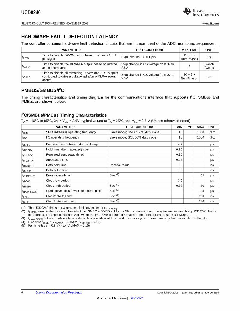
HARDWARE FAULT DETECTION LATENCY
PMBUS/SMBUS/I2C
I2C/SMBus/PMBus Timing Characteristics
UCD9240
SLUS766C–JULY 2008–REVISED NOVEMBER 2008................................................................................................................................................... www.ti.com
The controller contains hardware fault detection circuits that are independent of the ADC monitoring sequencer.PARAMETER TEST CONDITIONS MAX TIME UNIT
15 + 3 ×Time to disable DPWM output base on active FAULTtFAULT High level on FAULT pin µspin signal NumPhasesTime to disable the DPWM A output based on internal Step change in CS voltage from 0v to SwitchtCLF-A 4analog comparator 2.5V CyclesTime to disable all remaining DPWM and SRE outputs 10 + 3 ×Step change in CS voltage from 0V totCLF-B configured to drive a voltage rail after a CLF-A event µs2.5V NumPhasesoccurs
The timing characteristics and timing diagram for the communications interface that supports I2C, SMBus andPMBus are shown below.
TA = –40°C to 85°C, 3V < VDD < 3.6V, typical values at TA = 25°C and VCC = 2.5 V (Unless otherwise noted)
PARAMETER TEST CONDITIONS MIN TYP MAX UNITfSMB SMBus/PMBus operating frequency Slave mode; SMBC 50% duty cycle 10 1000 kHzfI2C I C operating frequency Slave mode; SCL 50% duty cycle 10 1000 kHz
t(BUF) Bus free time between start and stop 4.7 µst(HD:STA) Hold time after (repeated) start 0.26 µst(SU:STA) Repeated start setup timed 0.26 µst(SU:STO) Stop setup time 0.26 µst(HD:DAT) Data hold time Receive mode 0 nst(SU:DAT) Data setup time 50 nst(TIMEOUT) Error signal/detect See (1) 35 µst(LOW) Clock low period 0.5 µst(HIGH) Clock high period See (2) 0.26 50 µst(LOW:SEXT) Cumulative clock low slave extend time See (3) 25 µstFALL Clock/data fall time See (4) 120 nstRISE Clock/data rise time See (5) 120 ns
(1) The UCD9240 times out when any clock low exceeds t(TIMEOUT).(2) t(HIGH), max, is the minimum bus idle time. SMBC = SMBD = 1 for t > 50 ms causes reset of any transaction involving UCD9240 that is
in progress. This specification is valid when the NC_SMB control bit remains in the default cleared state (CLK[0]=0).(3) t(LOW:SEXT) is the cumulative time a slave device is allowed to extend the clock cycles in one message from initial start to the stop.(4) Rise time tRISE = VVILMAX – 0.15) to (VVIHMIN + 0.15)(5) Fall time tFALL = 0.9 VDD to (VILMAX – 0.15)
6 Submit Documentation Feedback Copyright © 2008, Texas Instruments Incorporated
Product Folder Link(s): UCD9240
UCD9240
www.ti.com ................................................................................................................................................... SLUS766C–JULY 2008–REVISED NOVEMBER 2008
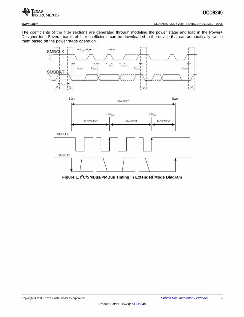
The coefficients of the filter sections are generated through modeling the power stage and load in the Power+Designer tool. Several banks of filter coefficients can be downloaded to the device that can automatically switchthem based on the power stage operation.
Figure 1. I2C/SMBus/PMBus Timing in Extended Mode Diagram
Copyright © 2008, Texas Instruments Incorporated Submit Documentation Feedback 7
Product Folder Link(s): UCD9240
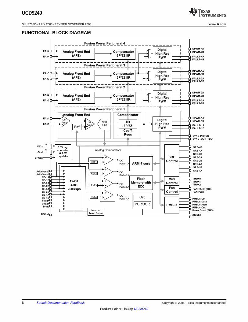
FUNCTIONAL BLOCK DIAGRAM
Compensator
3P/3Z IIR
12-bit
ADC
250 ksps
Osc
ARM-7 core
PMBus
EAp4
EAn4
EAp3
EAn3
EAp2
EAn2
AddrSens0
AddrSens1
CS-1A
CS-1B
CS-2A
CS-2B
CS-3A
CS-3B
CS-4A
CS-4B
Vin/Iin
Vtrack
Temp
V33x
xGnd
Analog Front End
(AFE)
Analog Front End
(AFE)
Analog Front End
(AFE)
Ref
ADC
6 bitIIR
3P/3Z
Err
Amp
EAp1
EAn1
Coeff.
Regs
CompensatorAnalog Front End
ADCref
POR/BOR
DPWM-1A
Ref 1
Analog Comparators
OC
PWM-1A
DPWM-1B
FAULT-1A
FAULT-1B
DPWM-2A
DPWM-2B
FAULT-2A
FAULT-2B
DPWM-3A
DPWM-3B
FAULT-3AFAULT-3B
DPWM-4A
DPWM-4B
FAULT-4A
FAULT-4B
PMBus-Clk
PMBus-Data
PMBus-Alert
PMBus-Cntl
PowerGood (TMS)
SYNC-IN (TDI)
SYNC -OUT (TDO)
5
6
BPCap
SRE-4B
SRE-4A
SRE-3B
SRE-3A
SRE-2B
SRE-2A
SRE-1B
SRE-1A
SRE
Control
Compensator
3P/3Z IIR
Compensator
3P/3Z IIR
Flash
Memory with
ECC
Diff
Amp
Fusion Power Peripheral 4
Fusion Power Peripheral 3
Fusion Power Peripheral 2
Fusion Power Peripheral 1
Internal
Temp Sense
3.3V reg.
controller
& 1.8V
regulator
Ref 2
Ref 3
Ref 4
Digital
High Res
PWM
Digital
High Res
PWM
Digital
High Res
PWM
Digital
High Res
PWM
Mux
Control
TMUX0
TMUX1
TMUX2
OC
PWM-2A
OC
PWM-3A
OC
PWM-4A
Fan
ControlFAN-TACH (TCK)
FAN-PWM
/RESET
260
UCD9240
SLUS766C–JULY 2008–REVISED NOVEMBER 2008................................................................................................................................................... www.ti.com
8 Submit Documentation Feedback Copyright © 2008, Texas Instruments Incorporated
Product Folder Link(s): UCD9240
58
46
45
7 44
47
9
62
6364
65
6667
6869
EAp1
EAn1EAp2
EAn2EAp3
EAn3
EAp4EAn4
AddrSen0AddrSen1
CS-1A (COMP1)CS-2A (COMP2)
CS-3A (COMP3)
CS-4A (COMP4)CS-1B
CS-2BCS-3B
CS-4B
Vin/IinVtrack
TempAux-in (AD13)
Aux-in (AD14)
ADCref
7776
75
43
279
78
7473
56
7
7271
1
DPWM-1A
DPWM-1BDPWM-2A
DPWM-2B
DPWM-3ADPWM-3B
DPWM-4ADPWM-4B
21
22
2324
2526
27
28
SRE-1A
SRE-1B
SRE-2ASRE-2B
SRE-3ASRE-3B
SRE-4A
SRE-4B
FAULT-1AFAULT-1B
FAULT-2A
FAULT-2BFAULT-3A
FAULT-3BFAULT-4A
FAULT-4B
1211
5137
38
5233
50
PMBus-Clk
PMBus-DataPMBus-Alert
PMBus-CtrlPowerGood
19
2035
36
49
V33
FB
V33
AV
33D
V33
DIO
-1
V33
DIO
-2B
PC
ap
70
58
57
8 56
59
A-1
VS
S
A-2
VS
S
A-3
VS
S
D-1
VS
S
D-2
VS
S
D-3
VS
S
61
60
80 9
34
55
/RESET13
48
47
4645
4414
15
1617
1829
41
4243
TMUX-0
TMUX-1TMUX-2
39
4054
SYNC-IN
SYNC-OUTFAN-PWM
FAN-TACHDiag LED
31
3053
32
10
UCD9240-64pin UCD9240-80pin
50
5152
53
5455
5657
EAp1
EAn1EAp2
EAn2EAp3
EAn3
EAp4EAn4
AddrSens0AddrSens1
CS-1A (COMP1)CS-2A (COMP2)
CS-3A (COMP3)
CS-4A (COMP4)CS-1B
CS-2BVin/Iin
Vtrack
Temp
6160
59
32
163
62
45
6
DPWM-1A
DPWM-1BDPWM-2A
DPWM-2B
DPWM-3ADPWM-4A
17
18
1920
2123
SRE-1A
SRE-1BSRE-2A
SRE-2BSRE-3A
SRE-4A
FAULT-1AFAULT-1B
FAULT-2AFAULT-2B
FAULT-3A
FAULT-4A22
2433
35
2930
PMBus-ClkPMBus-Data
PMBus-Alert
PMBus-CtrlPowerGood (TMS)
15
1627
2839
V33
FB
V33
A
V3
3D
V33
DIO
-1
V33
DIO
-2B
PC
ap
A-1
VS
S
A-2
VS
S
A-3
VS
S
D-1
VS
S
D-2
VS
S
D-3
VS
S
49
48
64 8
26
43
/RESET9
/TRST
TRCK
40
10
1112
13
1425
34
TMUX-0
TMUX-1
TMUX-2
3132
42
FAN-PWM
FAN-TACH (TCK)SYNC-IN (TDI)
SYNC-OUT (TDO)
41
3638
37
/TRSTTMS
TDI
TDOTCK
TRCK
UCD9240
www.ti.com ................................................................................................................................................... SLUS766C–JULY 2008–REVISED NOVEMBER 2008
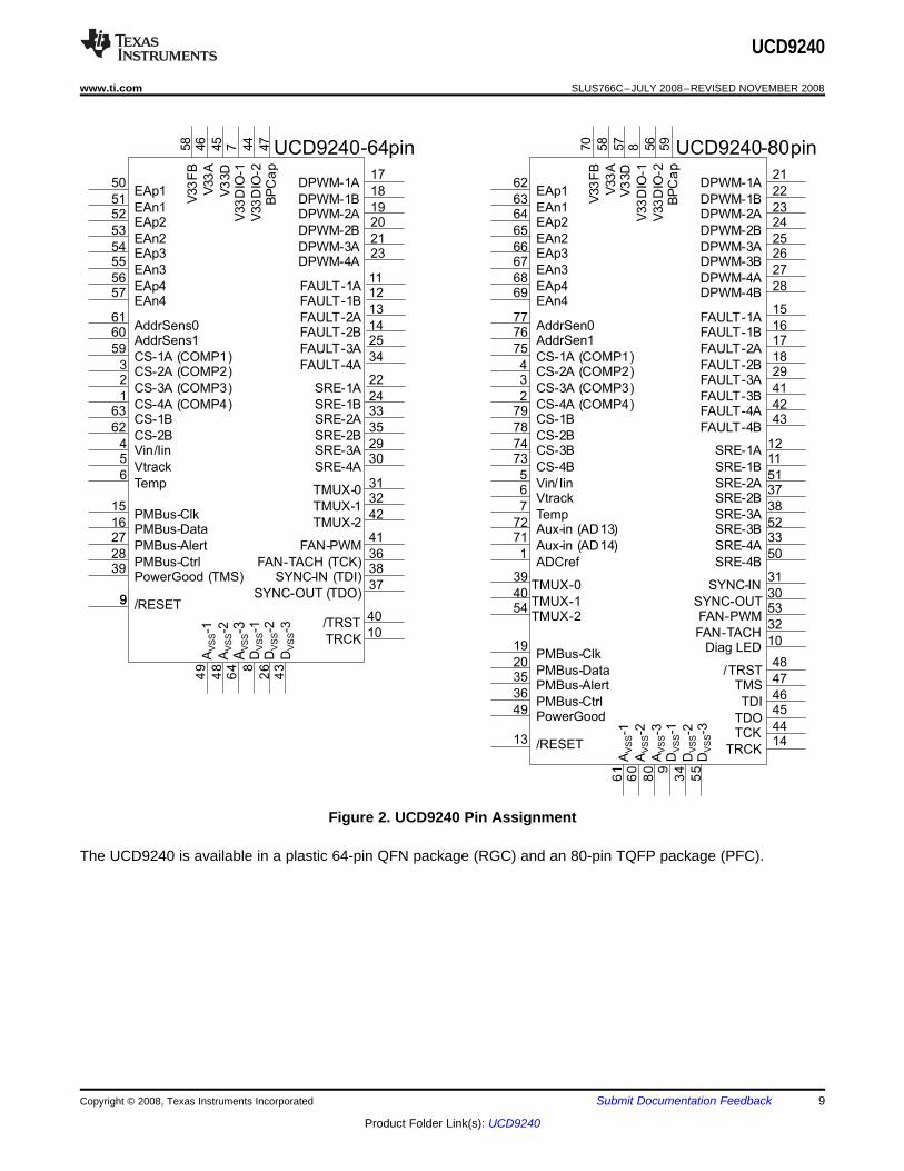
Figure 2. UCD9240 Pin Assignment
The UCD9240 is available in a plastic 64-pin QFN package (RGC) and an 80-pin TQFP package (PFC).
Copyright © 2008, Texas Instruments Incorporated Submit Documentation Feedback 9
Product Folder Link(s): UCD9240
TYPICAL APPLICATION SCHEMATIC
–Vsens-rail3
10 kW
0.1 mF
FCX491A+3.3 V
UCD9240RGC
53
52
51
50
57
56
55
54
47
44745
3
59
60
61
62
63
1
2
EAp1
EAn2
EAp2
EAn1
EAn4
EAp4
EAn3
EAp3
AddrSens1
AddrSens0
CS-1A(COMP1)
CS-2A(COMP2)
CS-2B
CS-1B
CS-4A(COMP4)
CS-3A(COMP3)
+Vsens-rail1
–Vsens-rail2
+Vsens-rail2
–Vsens-rail1
–Vsens-rail4
+Vsens-rail4
+Vsens-rail3
CS-rail2B
CS-rail1A
CS-rail4A
CS-rail3A
CS-rail2A
CS-rail1B
6
5
4
Temp
Vtrack
Vin/Iin
16
15
PMBus-Data
PMBus-Clk
39
28
27
PowerGood (TMS)
PMBus-Ctrl
PMBus-Alert
+3.3 V
46
52
V33F
B
V33A
V33D
V33D
IO-1
V33D
IO-2
BP
Cap
4.7 mF
20
19
18
17
12
11
23
21
DPWM-1A
15 kW
0.1 mF
34
25
14
13
24
22
35
33
30
29
32
31
42
FAN-Tach36
41FAN-PWM
SyncOut37
38SyncIn
10
40
DPWM-2B
DPWM-2A
DPWM-1B
FAULT-1B
FAULT-1A
DPWM-4A
DPWM-3A
FAULT-2A
FAULT-4A
FAULT-3A
FAULT-2B
SRE-1B
SRE-1A
SRE-2B
SRE-2A
SRE-4A
SRE-3A
TMUX-1
TMUX-0
TMUX-2
FAN-TACH
FAN-PWM
SYNC-OUT
SYNC-IN
RCR
TRST9RESET
10 kW
10 kW
VIN
49
48
64 8 26
Dgnd-2
Dgnd-1
Agnd-3
Agnd-2
Agnd-1
43
Dgnd-3
10 kW
14
13
A1
A0
1
12
15
A4
A3
A2
4
2
A7
A6
A55
8
11
10
6
S2
Com
S0
S1
EN
3
Temp-rail1B
Temp-rail1A
Temp-rail2B
Temp-rail2A
Temp-rail4A
Temp-rail3A
CD74HC4051
+3.3 V
16
PTD08A010W
FAULT
PWM
SRE
INH IOUT
PTD08A010W
FAULT
PWM
SRE
INH IOUT
Commutation
UCD7230 Driver
Logic
FAULT
PWM
SRE
INH
IOUT
Temp Sensor
PTD08A020W
Temp-rail1A
INH
+3.3 V
VIN
VO
PTD08A020W
FAULT
PWM
SRE
INH IOUT
Temp-rail1B
CS-rail1A
+Vsens-rail1–Vsens-rail1
Temp-rail2A
Temp-rail2B
+Vsens-rail2–Vsens-rail2
CS-rail1B
CS-rail2A
CS-rail2B
PTD08A010W
FAULT
PWM
SRE
INH IOUT
PTD08A010W
FAULT
PWM
SRE
INH IOUT
Temp-rail3A
Temp-rail4A
+Vsens-rail4–Vsens-rail4
CS-rail3A
CS-rail4A
+Vsens-rail3–Vsens-rail3
82.5 kW
TEMP
VOUT
GND
VBIAS
TEMP
GND
TEMP
VOUT
GND
TEMP
VOUT
GND
TEMP
VOUT
GND
TEMP
VOUT
GND
VBIAS VIN
VIN
VBIAS VIN
VIN
VBIAS VIN
VIN
VBIAS VIN
VIN
VBIAS VIN
VIN
[A]
UDG-08035
UCD9240
SLUS766C–JULY 2008–REVISED NOVEMBER 2008................................................................................................................................................... www.ti.com
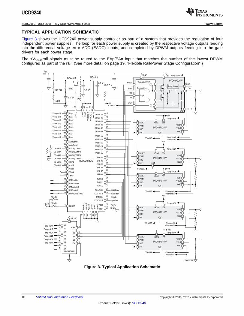
Figure 3 shows the UCD9240 power supply controller as part of a system that provides the regulation of fourindependent power supplies. The loop for each power supply is created by the respective voltage outputs feedinginto the differential voltage error ADC (EADC) inputs, and completed by DPWM outputs feeding into the gatedrivers for each power stage.
The ±Vsenserail signals must be routed to the EAp/EAn input that matches the number of the lowest DPWMconfigured as part of the rail. (See more detail on page 19, "Flexible Rail/Power Stage Configuration".)
Figure 3. Typical Application Schematic
10 Submit Documentation Feedback Copyright © 2008, Texas Instruments Incorporated
Product Folder Link(s): UCD9240

UCD9240
www.ti.com ................................................................................................................................................... SLUS766C–JULY 2008–REVISED NOVEMBER 2008
PIN DESCRIPTIONS64-PIN PACKAGE 80-PIN PACKAGE
I/O DESCRIPTIONPIN NO. SIGNAL PIN NO. SIGNAL
Error Amplifier Differential Analog Inputs50 EAp1 62 EAp1 AI Error analog, differential voltage. Positive channel #1 input.51 EAn1 63 EAn1 AI Error analog, differential voltage. Negative channel #1 input.52 EAp2 64 EAp2 AI Error analog, differential voltage. Positive channel #2 input.53 EAn2 65 EAn2 AI Error analog, differential voltage. Negative channel #2 input.54 EAp3 66 EAp3 AI Error analog, differential voltage. Positive channel #3 input.55 EAn3 67 EAn3 AI Error analog, differential voltage. Negative channel #3 input.56 EAp4 68 EAp4 AI Error analog, differential voltage. Positive channel #4 input.57 EAN4 69 EAn4 AI Error analog, differential voltage. Negative channel #4 input.
Analog Inputs61 AddrSens0 77 AddrSens0 AI PMBus address sense. Least significant address bits60 AddrSens1 76 AddrSens1 AI PMBus address sense. Most significant address bits59 CS-1A 75 CS-1A AI Power stage 1A current sense input. Analog comparator 13 CS-2A 4 CS-2A AI Power stage 2A current sense input. Analog comparator 22 CS-3A 3 CS-3A AI Power stage 3A current sense input. Analog comparator 31 CS-4A 2 CS-4A AI Power stage 4A current sense input. Analog comparator 463 CS-1B 79 CS-1B AI Power stage 1B current sense input62 CS-2B 78 CS-2B AI Power stage 2B current sense input– CS-3B 74 CS-3B AI Power stage 3B current sense input– CS-4B 73 CS-4B AI Power stage 4B current sense input4 Vin/ Iin 5 Vin/ Iin AI Input supply sense, alternates between Vin and Iin5 VTRACK 6 VTRACK AI Voltage tracking6 Temp 7 Temp AI Temperature sense input
Aux-in Aux-in– 72 AI Unused analog input -- Tie to ground with 10 kΩ resistor(AD13) (AD13)Aux-in Aux-in– 71 AI Unused analog input -- Tie to ground with 10 kΩ reisistor(AD14) (AD14)
– ADCref 1 ADCref AI ADC Decoupling Capacitor -- Tie 0.1 µF cap to ground
Digital PWM Outputs17 dPWM-1A 21 dPWM-1A O DPWM 1A output18 dPWM-1B 22 dPWM-1B O DPWM 1B output19 dPWM-2A 23 dPWM-2A O DPWM 2A output20 dPWM-2B 24 dPWM-2B O DPWM 2B output21 dPWM-3A 25 dPWM-3A O DPWM 3A output
26 dPWM-3B O DPWM 3B output23 dPWM-4A 27 dPWM-4A O DPWM 4A output
28 dPWM-4B O DPWM 4B output
External Fault Inputs11 FAULT-1A 15 FAULT-1A I External fault input 1A12 FAULT-1B 16 FAULT-1B I External fault input 1B13 FAULT-2A 17 FAULT-2A I External fault input 2A14 FAULT-2B 18 FAULT-2B I External fault input 2B25 FAULT-3A 29 FAULT-3A I External fault input 3A
41 FAULT-3B I External fault input 3B34 FAULT-4A 42 FAULT-4A I External fault input 4A
43 FAULT-4B I External fault input 4B
Copyright © 2008, Texas Instruments Incorporated Submit Documentation Feedback 11
Product Folder Link(s): UCD9240

UCD9240
SLUS766C–JULY 2008–REVISED NOVEMBER 2008................................................................................................................................................... www.ti.com
PIN DESCRIPTIONS (continued)64-PIN PACKAGE 80-PIN PACKAGE
I/O DESCRIPTIONPIN NO. SIGNAL PIN NO. SIGNAL
Synchronous Rectification Enable Outputs22 SRE-1A 12 SRE-1A O Synchronous rectifier enable 1A24 SRE-1B 11 SRE-1B O Synchronous rectifier enable 1B33 SRE-2A 51 SRE-2A O Synchronous rectifier enable 2A35 SRE-2B 37 SRE-2B O Synchronous rectifier enable 2B29 SRE-3A 38 SRE-3A O Synchronous rectifier enable 3A
52 SRE-3B O Synchronous rectifier enable 3B30 SRE-4A 33 SRE-4A O Synchronous rectifier enable 4A
50 SRE-4B O Synchronous rectifier enable 4B
Miscellaneous Digital I/O31 TMUX-0 39 TMUX-0 O Temperature multiplexer select S09 RESET 13 RESET I Active low device reset input32 TMUX-1 40 TMUX-1 O Temperature multiplexer select S142 TMUX-2 54 TMUX-2 O Temperature multiplexer select S241 FAN-PWM 53 FAN-PWM O Fan control PWM output39 PowerGood 49 PowerGood O Power good signal (multiplexed with TMS on 64-pin package)36 FAN-Tach 32 FAN-Tach I Fan tachometer input (multiplexed with TCK on 64-pin package)
Synchronization output from DPWM (multiplexed with TDO on 64-pin37 Sync_Out 30 Sync_Out O package)38 Sync_In 31 Sync_In I Synchronization input to DPWM (multiplexed with TDI on 64-pin package)
10 diag LED O Diagnostic LED
PMBus Communications Interface15 PMBus_Clk 19 PMBus_Clk I/O PMBus Clk (Must have pullup to 3.3 V)16 PMBus_Data 20 PMBus_Data I/O PMBus Data (Must have pullup to 3.3 V)27 PMBus_Alert 35 PMBus_Alert O PMBUS Alert28 PMBus_Cntrl 36 PMBus_Cntrl I PMBUS Cntl
JTAG10 TRCK 14 TRCK O Test return clock36 TCK 44 TCK I Test clock (multiplexed with FAN-Tach (TCK) on 64-pin package)37 TDO 45 TDO O Test data out (multiplexed with Sync_Out (TDO) on 64-pin package)
Test data in -- tie to Vdd with 10 kΩ resistor (multiplexed with Sync_In38 TDI 46 TDI I (TDI) on 64-pin package)Test mode select -- tie to Vdd with 10 kΩ resistor (multiplexed with39 TMS 47 TMS I/O PowerGood (TMS) on 64-pin package)
40 TRST 48 TRST I/O Test reset -- tie to ground with 10 kΩ resistor
Input Power and Grounds58 V33FB 70 V33FB O 3.3-V linear regulator Feedback connection46 V33A 58 V33A I Analog 3.3-V supply45 V33D 57 V33D I Digital core 3.3-V supply7 V33DIO 8 V33DIO I Digital I/O 3.3-V supply44 V33DIO 56 V33DIO I Digital I/O 3.3-V supply47 BPCap 59 BPCap I 1.8-V bypass capacitor connection49 AVSS 61 AVSS I Analog ground48 AVSS 60 AVSS I Analog ground64 AVSS 80 AVSS I Analog ground
12 Submit Documentation Feedback Copyright © 2008, Texas Instruments Incorporated
Product Folder Link(s): UCD9240
FUNCTIONAL OVERVIEW
PMBus Interface
Resistor Programmed PMBus Address Decode
Vdd
10 uA
IBIAS
To 12-bit ADC
Resistor to
set PMBus
Address
On/Off Control
AddrSens0,AddrSens1pins
UCD9240
UCD9240
www.ti.com ................................................................................................................................................... SLUS766C–JULY 2008–REVISED NOVEMBER 2008
PIN DESCRIPTIONS (continued)64-PIN PACKAGE 80-PIN PACKAGE
I/O DESCRIPTIONPIN NO. SIGNAL PIN NO. SIGNAL
8 DVSS 9 DVSS I Digital ground26 DVSS 34 DVSS I Digital ground43 DVSS 55 DVSS I Digital ground
Power It is recommended that this pad be connected to analog ground. (64-pinNo Connect n/a n/a IPad package only)
The UCD9240 contains four fusion power peripherals (FPP). Each FPP can be configured to regulated up to fourDC/DC converter outputs. There are eight PWM outputs that can be assigned to drive the coverter outputs. EachFPP can be configured to drive from one of the eight power stages. Each FPP consists of:• A differential input error voltage amplifier.• A 10-bit DAC used to set the output regulation reference voltage.• A fast ADC with programmable input gain to digitally measure the error voltage.• A dedicated 3-pole/3-zero digital filter to compensate the error voltage.• A digital PWM (DPWM) engine that generates the PWM pulse width based on the compensator output.
Each controller is configured through a PMBus serial interface.
The PMBus is a serial interface specifically designed to support power management. It is based on the SMBusinterface that is built on the I2C physical specification. The UCD9240 supports revision 1.1 of the PMBusstandard. Wherever possible, standard PMBus commands are used to support the function of the device. Forunique features of the UCD9240, MFR_SPECIFIC commands are defined to configure or activate those features.These commands are defined in the UCD92xx PMBUS Command Reference.
The UCD9240 is PMBus compliant, in accordance with the "Compliance" section of the PMBus specification. Thefirmware is also compliant with the SMBus 1.1 specification, including support for the SMBus ALERT function.The hardware can support either 100 kHz, 400 kHz, or 1 MHz PMBus operation.
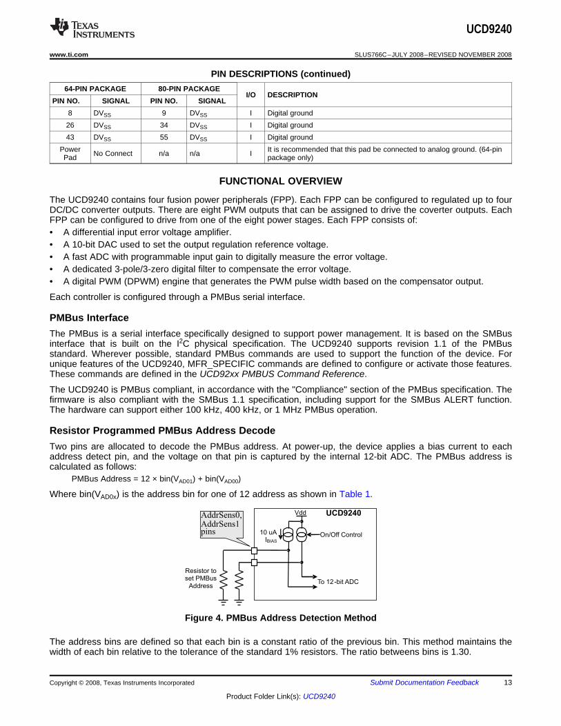
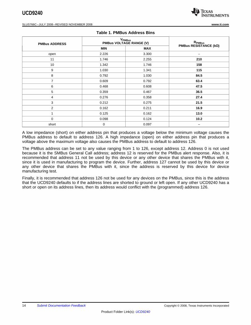
Two pins are allocated to decode the PMBus address. At power-up, the device applies a bias current to eachaddress detect pin, and the voltage on that pin is captured by the internal 12-bit ADC. The PMBus address iscalculated as follows:
PMBus Address = 12 × bin(VAD01) + bin(VAD00)
Where bin(VAD0x) is the address bin for one of 12 address as shown in Table 1.
Figure 4. PMBus Address Detection Method
The address bins are defined so that each bin is a constant ratio of the previous bin. This method maintains thewidth of each bin relative to the tolerance of the standard 1% resistors. The ratio betweens bins is 1.30.
Copyright © 2008, Texas Instruments Incorporated Submit Documentation Feedback 13
Product Folder Link(s): UCD9240
UCD9240
SLUS766C–JULY 2008–REVISED NOVEMBER 2008................................................................................................................................................... www.ti.com
Table 1. PMBus Address BinsVPMBus RPMBusPMBus VOLTAGE RANGE (V)PMBus ADDRESS PMBus RESISTANCE (kΩ)
MIN MAXopen 2.226 3.300 –
11 1.746 2.255 21010 1.342 1.746 1589 1.030 1.341 1158 0.792 1.030 84.57 0.609 0.792 63.46 0.468 0.608 47.55 0.359 0.467 36.54 0.276 0.358 27.43 0.212 0.275 21.52 0.162 0.211 16.91 0.125 0.162 13.00 0.098 0.124 10.2
short 0 0.097 –
A low impedance (short) on either address pin that produces a voltage below the minimum voltage causes thePMBus address to default to address 126. A high impedance (open) on either address pin that produces avoltage above the maximum voltage also causes the PMBus address to default to address 126.
The PMBus address can be set to any value ranging from 1 to 126, except address 12. Address 0 is not usedbecause it is the SMBus General Call address; address 12 is reserved for the PMBus alert response. Also, it isrecommended that address 11 not be used by this device or any other device that shares the PMBus with it,since it is used in manufacturing to program the device. Further, address 127 cannot be used by this device orany other device that shares the PMBus with it, since the address is reserved by this device for devicemanufacturing test.
Finally, it is recommended that address 126 not be used for any devices on the PMBus, since this is the addressthat the UCD9240 defaults to if the address lines are shorted to ground or left open. If any other UCD9240 has ashort or open on its address lines, then its address would conflict with the (programmed) address 126.
14 Submit Documentation Feedback Copyright © 2008, Texas Instruments Incorporated
Product Folder Link(s): UCD9240
JTAG Interface
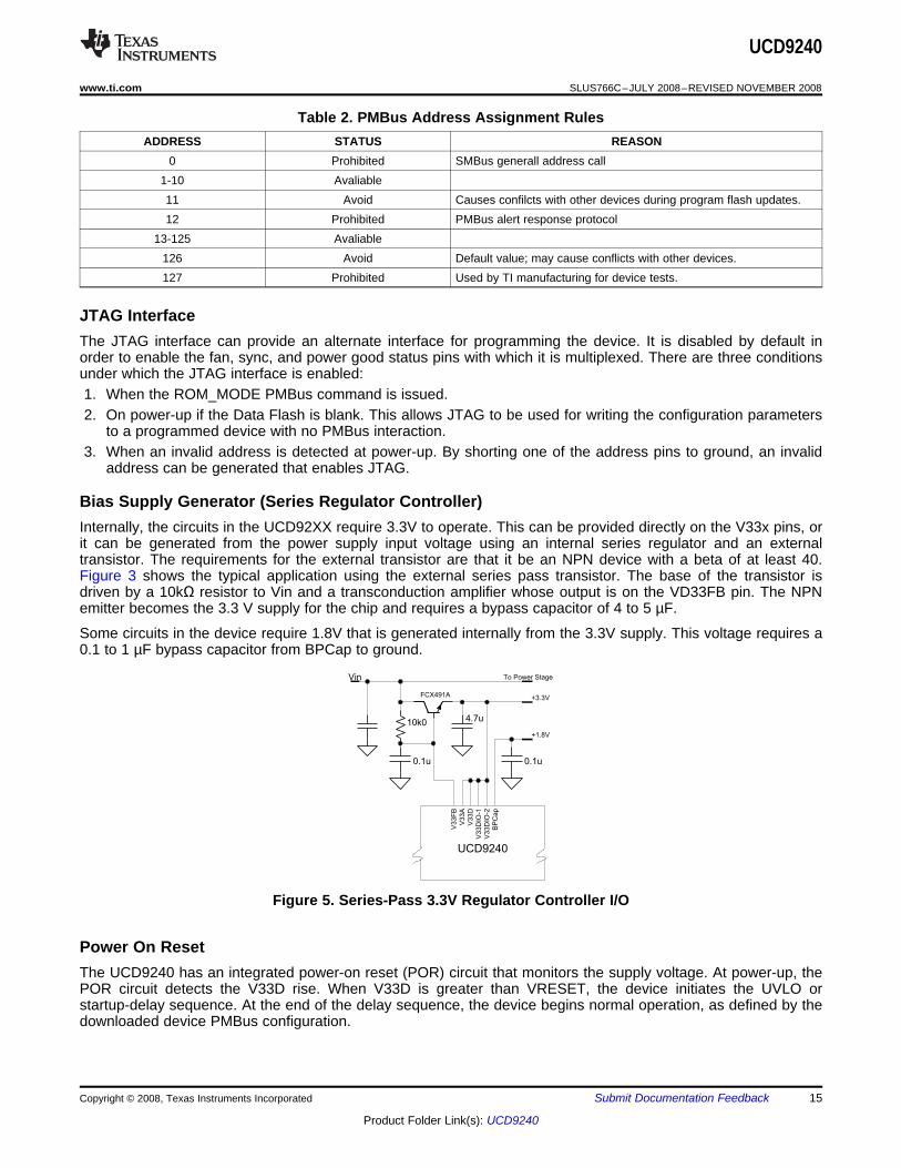
Bias Supply Generator (Series Regulator Controller)
V33F
B
V33A
V33D
V33D
IO-1
V33D
IO-2
BP
Cap
0.1u
10k0
Vin
4.7u
0.1u
FCX491A
UCD9240
To Power Stage
+3.3V
+1.8V
Power On Reset
UCD9240
www.ti.com ................................................................................................................................................... SLUS766C–JULY 2008–REVISED NOVEMBER 2008
Table 2. PMBus Address Assignment RulesADDRESS STATUS REASON
0 Prohibited SMBus generall address call1-10 Avaliable11 Avoid Causes confilcts with other devices during program flash updates.12 Prohibited PMBus alert response protocol
13-125 Avaliable126 Avoid Default value; may cause conflicts with other devices.127 Prohibited Used by TI manufacturing for device tests.
The JTAG interface can provide an alternate interface for programming the device. It is disabled by default inorder to enable the fan, sync, and power good status pins with which it is multiplexed. There are three conditionsunder which the JTAG interface is enabled:1. When the ROM_MODE PMBus command is issued.2. On power-up if the Data Flash is blank. This allows JTAG to be used for writing the configuration parameters
to a programmed device with no PMBus interaction.3. When an invalid address is detected at power-up. By shorting one of the address pins to ground, an invalid
address can be generated that enables JTAG.
Internally, the circuits in the UCD92XX require 3.3V to operate. This can be provided directly on the V33x pins, orit can be generated from the power supply input voltage using an internal series regulator and an externaltransistor. The requirements for the external transistor are that it be an NPN device with a beta of at least 40.Figure 3 shows the typical application using the external series pass transistor. The base of the transistor isdriven by a 10kΩ resistor to Vin and a transconduction amplifier whose output is on the VD33FB pin. The NPNemitter becomes the 3.3 V supply for the chip and requires a bypass capacitor of 4 to 5 µF.
Some circuits in the device require 1.8V that is generated internally from the 3.3V supply. This voltage requires a0.1 to 1 µF bypass capacitor from BPCap to ground.
Figure 5. Series-Pass 3.3V Regulator Controller I/O
The UCD9240 has an integrated power-on reset (POR) circuit that monitors the supply voltage. At power-up, thePOR circuit detects the V33D rise. When V33D is greater than VRESET, the device initiates the UVLO orstartup-delay sequence. At the end of the delay sequence, the device begins normal operation, as defined by thedownloaded device PMBus configuration.
Copyright © 2008, Texas Instruments Incorporated Submit Documentation Feedback 15
Product Folder Link(s): UCD9240
External Reset
Output Voltage Adjustment
VOUT_MARGIN_HIGH
VOUT_CAL_OFFSET
VOUT_MARGIN_LOW
VOUT_COMMAND + LimiterVOUT_
SCALE_
LOOP
“Reference
Voltage
Equivalent”
OPERATION
Command
VOUT_MAX
3:1
Mux
Analog Front End (AFE)
EApx
EAnx
6-bit result
eADC
Vref DAC
CPU
PMBus
GAFE = 1, 2, 4 or 8
Vead
GeADC = 8mV/LSB
Vref = 1.563 mV/LSB
+
+
UCD9240
SLUS766C–JULY 2008–REVISED NOVEMBER 2008................................................................................................................................................... www.ti.com
The device can be forced into the reset state by an external circuit connected to the RESET pin. A logic lowvoltage on this pin holds the device in reset. To avoid an erroneous trigger caused by noise, a pull up resistor to3.3V is recommended.
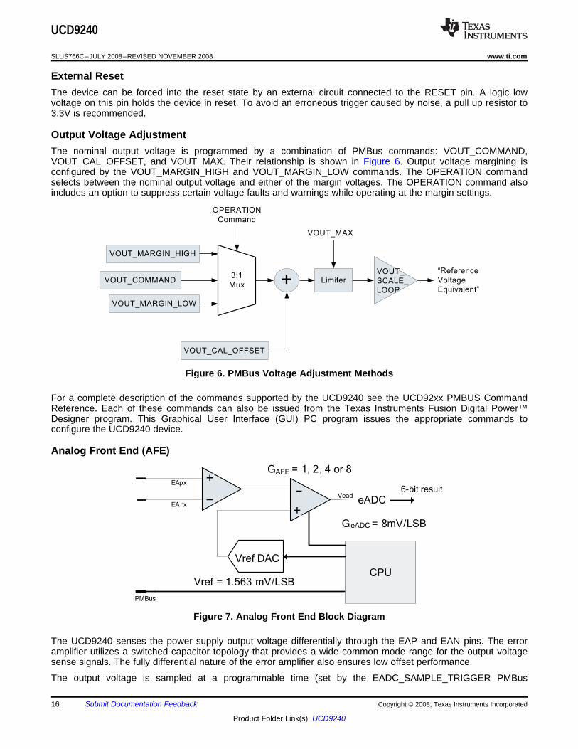
The nominal output voltage is programmed by a combination of PMBus commands: VOUT_COMMAND,VOUT_CAL_OFFSET, and VOUT_MAX. Their relationship is shown in Figure 6. Output voltage margining isconfigured by the VOUT_MARGIN_HIGH and VOUT_MARGIN_LOW commands. The OPERATION commandselects between the nominal output voltage and either of the margin voltages. The OPERATION command alsoincludes an option to suppress certain voltage faults and warnings while operating at the margin settings.
Figure 6. PMBus Voltage Adjustment Methods
For a complete description of the commands supported by the UCD9240 see the UCD92xx PMBUS CommandReference. Each of these commands can also be issued from the Texas Instruments Fusion Digital Power™Designer program. This Graphical User Interface (GUI) PC program issues the appropriate commands toconfigure the UCD9240 device.
Figure 7. Analog Front End Block Diagram
The UCD9240 senses the power supply output voltage differentially through the EAP and EAN pins. The erroramplifier utilizes a switched capacitor topology that provides a wide common mode range for the output voltagesense signals. The fully differential nature of the error amplifier also ensures low offset performance.
The output voltage is sampled at a programmable time (set by the EADC_SAMPLE_TRIGGER PMBus
16 Submit Documentation Feedback Copyright © 2008, Texas Instruments Incorporated
Product Folder Link(s): UCD9240
EAp
EAn
VOUT
R1
RIN
IOFF
R2
2 1 2
1 2 1 2
1 2 1 2
= +æ ö æ ö
+ + + +ç ÷ ç ÷è ø è ø
EA OUT OFF
IN IN
R R RV V I
R R R RR R R R
R R
1
2
1
11
=æ ö
- + ±ç ÷è ø
EA
OUT EA OFF
IN
R VR
RV V R I
R
Digital Compensator
UCD9240
www.ti.com ................................................................................................................................................... SLUS766C–JULY 2008–REVISED NOVEMBER 2008
command). When the differential input voltage is sampled, the voltage is captured in internal capacitors and thentransferred to the error amplifier where the value is subtracted from the set-point reference which is generated bythe Vref DAC as shown in Figure 7. The resulting error voltage is then amplified by a programmable gain circuitbefore the error voltage is converted to a digital value by the flash ADC. This programmable gain is configuredthrough the PMBus and affects the dynamic range and resolution of the sensed error voltage as shown inTable 3.
Table 3. Analog Front End ResolutionAFE_GAIN for PMBus EFFECTIVE ADCAFE GAIN DIGITAL ERROR VOLTAGE DYNAMIC RANGE (mV)COMMAND RESOLUTION (mV)
1 0 8 -256 to 2482 1 4 -128 to 1244 2 2 -64 to 628 3 1 -32 to 31
The AFE variable gain is one of the compensation coefficients that are stored when the device is configured byissuing the CLA_GAINS PMBus command. Compensator coefficients are arranged in several banks: one bankfor start/stop ramp or tracking, one bank for normal regulation mode and one bank for light load mode. Thisallows the user to trade-off resolution and dynamic range for each operational mode.
The EADC, which samples the error voltage, has high accuracy, high resolution, and a fast conversion time.However, its range is limited as shown in Table 3. If the output voltage is different from the reference by morethan this, the EADC reports a saturated value at -32 LSBs or 31 LSBs. The UCD9240 overcomes this limitationby adjusting the setpoint DAC up or down in order to bring the error voltage out of saturation. In this way, theeffective range of the ADC is extended. When the EADC saturates, the setpoint DAC is slewed at a rate of 0.156V/ms, referred to the EA differential inputs.
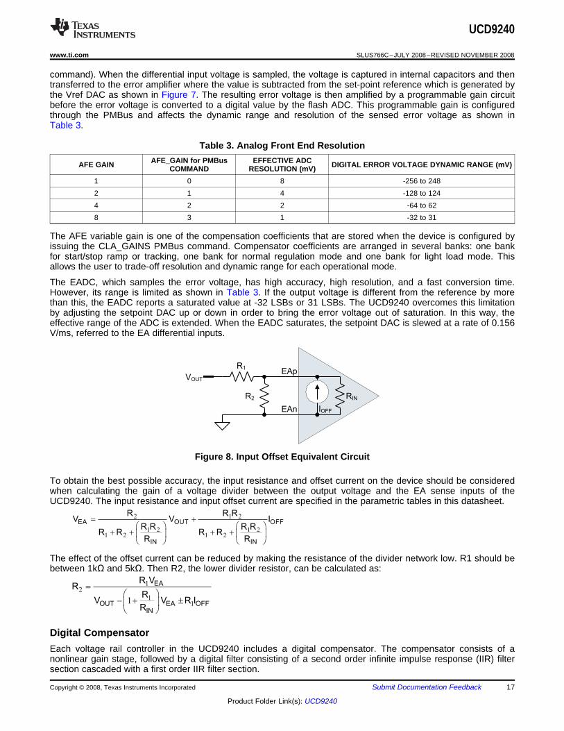
Figure 8. Input Offset Equivalent Circuit
To obtain the best possible accuracy, the input resistance and offset current on the device should be consideredwhen calculating the gain of a voltage divider between the output voltage and the EA sense inputs of theUCD9240. The input resistance and input offset current are specified in the parametric tables in this datasheet.
The effect of the offset current can be reduced by making the resistance of the divider network low. R1 should bebetween 1kΩ and 5kΩ. Then R2, the lower divider resistor, can be calculated as:
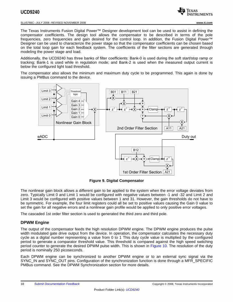
Each voltage rail controller in the UCD9240 includes a digital compensator. The compensator consists of anonlinear gain stage, followed by a digital filter consisting of a second order infinite impulse response (IIR) filtersection cascaded with a first order IIR filter section.
Copyright © 2008, Texas Instruments Incorporated Submit Documentation Feedback 17
Product Folder Link(s): UCD9240
Nonlinear Gain Block
Threshold
logic
Gain 0
Gain 1
Gain 2
Gain 3
Gain 4
eADC
Limit 0
Limit 3
Limit 2
Limit 1z
-1 +
X
X
B01
z-1
X
B11
X
B21
+
Clamp z-1z
-1
X
X
+
A11 A21
z-1X +
B12
z-1
Clamp
X
A21
2nd Order Filter Section
1st Order Filter Section
Duty out
DPWM Engine
UCD9240
SLUS766C–JULY 2008–REVISED NOVEMBER 2008................................................................................................................................................... www.ti.com
The Texas Instruments Fusion Digital Power™ Designer development tool can be used to assist in defining thecompensator coefficients. The design tool allows the compensator to be described in terms of the polefrequencies, zero frequencies and gain desired for the control loop. In addition, the Fusion Digital Power™Designer can be used to characterize the power stage so that the compensator coefficients can be chosen basedon the total loop gain for each feedback system. The coefficients of the filter sections are generated throughmodeling the power stage and load.
Additionally, the UCD9240 has three banks of filter coefficients: Bank-0 is used during the soft start/stop ramp ortracking; Bank-1 is used while in regulation mode; and Bank-2 is used when the measured output current isbelow the configured light load threshold.
The compensator also allows the minimum and maximum duty cycle to be programmed. This again is done byissuing a PMBus command to the device.
Figure 9. Digital Compensator
The nonlinear gain block allows a different gain to be applied to the system when the error voltage deviates fromzero. Typically Limit 0 and Limit 1 would be configured with negative values between -1 and -32 and Limit 2 andLimit 3 would be configured with positive values between 1 and 31. However, the gain thresholds do not have tobe symmetric. For example, the four limit registers could all be set to positive values causing the Gain 0 value toset the gain for all negative errors and a nonlinear gain profile would be applied to only positive error voltages.
The cascaded 1st order filter section is used to generated the third zero and third pole.
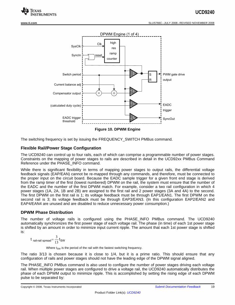
The output of the compensator feeds the high resolution DPWM engine. The DPWM engine produces the pulsewidth modulated gate drive output from the device. In operation, the compensator calculates the necessary dutycycle as a digital number representing a value from 0 to 1 This duty cycle value is multiplied by the configuredperiod to generate a comparator threshold value. This threshold is compared against the high speed switchingperiod counter to generate the desired DPWM pulse width. This is shown in Figure 10. The resolution of the dutyperiod is nominally 250 picoseconds.
Each DPWM engine can be synchronized to another DPWM engine or to an external sync signal via theSYNC_IN and SYNC_OUT pins. Configuration of the synchronization function is done through a MFR_SPECIFICPMBus command. See the DPWM Synchronization section for more details.
18 Submit Documentation Feedback Copyright © 2008, Texas Instruments Incorporated
Product Folder Link(s): UCD9240
high
res
ramp
counter
Clk
reset
Switch period
Current balance adj
Compensator output
(calculated duty cycle)
EADC triggerthreshold
PWM gate drive
output
SysClk
SyncIn
EADC
trigger
SyncOut
S
R
DPWM Engine (1 of 4)
Flexible Rail/Power Stage Configuration
DPWM Phase Distribution
3
13=rail-rail spread SWt t
UCD9240
www.ti.com ................................................................................................................................................... SLUS766C–JULY 2008–REVISED NOVEMBER 2008
Figure 10. DPWM Engine
The switching frequency is set by issuing the FREQUENCY_SWITCH PMBus command.
The UCD9240 can control up to four rails, each of which can comprise a programmable number of power stages.Constraints on the mapping of power stages to rails are described in detail in the UCD92xx PMBus CommandReference under the PHASE_INFO command.
While there is significant flexibility in terms of mapping power stages to output rails, the differential voltagefeedback signals (EAP/EAN) cannot be re-mapped through any commands, and therefore, must be connected tothe proper input on the circuit board. Because the EADC sample trigger for a given front end stage is derivedfrom the ramp timer of the first (lowest numbered) DPWM on the rail, the system must ensure that the number ofthe EADC and the number of the first DPWM match. For example, consider a two rail configuration in which 4power stages (1A, 2A, 1B and 2B) are assigned to the first rail and 2 power stages (3A and 4A) to the second.The first DPWM on the first rail is 1; its voltage feedback must be through EAP1/EAN1. The first DPWM on thesecond rail is 3; its voltage feedback must be through EAP3/EAN3. (In this configuration EAP2/EAN2 andEAP4/EAN4 are unused and are disabled to reduce unnecessary power consumption.)
The number of voltage rails is configured using the PHASE_INFO PMBus command. The UCD9240automatically synchronizes the first power stage of each voltage rail. The phase (in time) of each 1st power stageis shifted by an amount in order to minimize input current ripple. The amount that each 1st power stage is shiftedis:
Where tSW is the period of the rail with the fastest switching frequency.
The ratio 3/13 is chosen because it is close to 1/4, but it is a prime ratio. This should ensure that anyconfiguration of rails and power stages should not have the leading edge of the DPWM signal aligned.
The PHASE_INFO PMBus command is also used to configure the number of power stages driving each voltagerail. When multiple power stages are configured to drive a voltage rail, the UCD9240 automatically distributes thephase of each DPWM output to minimize ripple. This is accomplished by setting the rising edge of each DPWMpulse to be separated by:
Copyright © 2008, Texas Instruments Incorporated Submit Documentation Feedback 19
Product Folder Link(s): UCD9240
=SW
phase-phase spreadPhases
tt
N
DPWM Synchronization
Phase Shedding at Light Current Load
Phase Adding at Normal Current Load
Output Current Measurment
UCD9240
SLUS766C–JULY 2008–REVISED NOVEMBER 2008................................................................................................................................................... www.ti.com
Where tSW is the switching period and NPhases is the number of power stages driving a voltage rail.
DPWM synchronization provides a method to link the timing between rails on two distinct devices at the switchingrate; i.e., two rails on different devices can be configured to run at the same frequency and sync forcing them notto drift from each other. (Note that within a single device, because all rails are driven off a common clock there isno need for an internal sync because rails wont drift.)
The PMBus SYNC_IN_OUT command sets which rails (if any) should follow the sync input, and which rail (ifany) should drive the sync output.
For rails that are following the sync input, the DPWM ramp timer for that output is reset when the sync input goeshigh. This allows the slave device to sync to inputs that are either faster or slower than it is. On the fast side,there is no limit to how much faster the input is compared to the defined frequency of the rail; when the pulsecomes in, the timer is reset and the frequencies are locked. This is the standard mode of operation - setting theslave to run slower, and letting the sync speed it up.
If the slave rail is running fast, the sync pulse resets the counter after the DPWM output has already been turnedon. Resetting the counter at this point results in a larger duty cycle for that period. Because the system is closedloop; however, the controller reacts by decreasing the commanded control effort, with the result being aregulated rail synchronized to a slower master. Synchronizing to the slower master does have a limit however. Ifthe master is slow enough that the DPWM output has sufficient time to output the entire command pulse beforethe sync input arrives, the result is a double pulse. This is likely an undesirable mode of operation.
The Sync Input and Output Configuration Word set by the PMBus command consists of two bytes. The upperbyte (sync_out) controls which rail drives the sync output signal (0=DWPM1, 1=DPWM2, 2=DPWM3, 3=DPWM4.Any other value disables sync_out). The lower byte (sync_in) determines which rail(s) respond to the sync inputsignal (each bit represents one rail - note that multiple rails can be synchronized to the input). The DPWM periodis aligned to the sync input. For more information, see the UCD92xx PMBUS Command Reference.
Note that once a rail is synchronized to an external source, the rail-to-rail spacing that attempts to minimize inputcurrent ripple are lost. Rail-to-rail spacing can only be restored by power cycling or issuing a SOFT_RESETcommand.
By issuing LIGHT_LOAD_LIMIT_LOW, LIGHT_LOAD_LIMIT_HIGH, and LIGHT_LOAD_CONFIG commands, theUCD9240 can be configured to shed (disable) power stages when at light load. When this feature is enabled, thedevice disables the configured number of power stages when the average current drops below the specifiedLIGHT_LOAD_LIMIT_LOW. In addition, a separate set of compensation coefficients can be loaded into thedigital compensator when entering a light load condition.
After shedding phases, if the current load is increased past the LIGHT_LOAD_LIMIT_HIGH threshold, all phasesare re-enabled. If the compensator was configured for light load, the normal load coefficients are restored aswell. See the UCD92xx PMBUS Command Reference for more information.
Pins CS-1A, CS-1B, CS-2A, CS-2B, CS-3A, CS-3B, CS-4A, and CS-4B are used to measure either outputcurrent or inductor current in each of the controlled power stages. PMBus commands IOUT_CAL_GAIN andIOUT_CAL_OFFSET are used to calibrate each measurement. See the UCD92xx PMBus Command Referencefor specifics on configuring this voltage to current conversion.
When the measured current is outside the range of either the overcurrent or undercurrent threshold, a FAULT is
20 Submit Documentation Feedback Copyright © 2008, Texas Instruments Incorporated
Product Folder Link(s): UCD9240

Figure 1 Averaging filter for current monitoring
10 100 1.0k 10k 100k-50
-45
-40
-35
-30
-25
-20
-15
-10
-5
0
dB
freq in Hz
Output Current Balancing
UCD9240
www.ti.com ................................................................................................................................................... SLUS766C–JULY 2008–REVISED NOVEMBER 2008
declared and the UCD9240 performs the PMBus configured fault recovery. ADC current measurements aredigitally averaged before they are compared against the FAULT threshold. The output current is measured at arate of one output rail per 200 microseconds. The current measurements are then passed through a smoothingfilter to reduce noise on the signal and prevent false errors. The output of the smoothing filter asymptoticallyapproaches the input value with a time constant that is approximately 3.5 times the sampling interval.
Table 4. Output Current Filter Times ConstantsOUTPUT CURRENT SAMPLINGNUMBER OF OUTPUT RAILS FILTER TIME CONSTANTS (ms)INTERVALS (µs)
1 200 0.72 400 1.43 600 2.14 800 2.8
For example, with a single rail, the filter has the transfer function characteristics (Figure 11) that shows the signalmagnitude at the output of the averaging filter due to a sine wave input for a range of frequencies. This plotincludes an RC analog low pass network, with a corner frequency of 3 kHz, on the current sense inputs.
This averaged current measurement is used for output current fault detection; see “Overcurrent Detection,”below.
In response to a PMBus request for a current reading, the device returns an average current value. When theUCD9240 is configured to drive a multi-phase power converter, the device adds the average currentmeasurement for each of the power stages tied to a power rail.
Figure 11. Averaging Filter for Current Monitoring
When the UCD9240 is configured to drive multiple power stage circuits from one compensator, current balancingis implemented by adjusting each gate drive output pulse width to correct for current imbalance between theconnected power stage sections. The UCD9240 balances the current by monitoring the current at the CS analoginput for each power stage and then adding a current balance adjustment value to the DPWM ramp thresholdvalue for each power stage.
When there is more than one power stage connected to the voltage rail, the device continually determines whichstage has the highest measured current and which stage has the lowest measured current. To balance thecurrents while maintaining a constant total current, the adjustment value for the power stage with the lowestcurrent is increased by the same amount as the adjustment value for the power stage with the highest current isdecreased. A slight modification to this algorithm is made to keep the adjustment values positive in order toensure that a positive DPWM duty cycle is commanded under all conditions.
Copyright © 2008, Texas Instruments Incorporated Submit Documentation Feedback 21
Product Folder Link(s): UCD9240
Overcurrent Detection
( ) ( )1 2 11 e
t-æ ö
ç ÷= + - -ç ÷è ø
smoothed
t
I tI I I
(3)
2 1
2
lntæ ö-
= ç ÷-è ø
laglimit
I It
I I (4)
Current Foldback Mode
UCD9240
SLUS766C–JULY 2008–REVISED NOVEMBER 2008................................................................................................................................................... www.ti.com
Several mechanisms are provided to sense output current fault conditions. This allows for the design of powersystems with multiple layers of protection.1. A logic high signal on the FAULT input causes a hardware interrupt to the internal CPU. The CPU then
determines which DPWM outputs are configured to be associated with the voltage rail that contained the faultand disables those DPWM and SRE outputs. This process takes about 14 microseconds. An integrated gatedriver such as the UCD7230 can be used to generate the FAULT signal. The UCD7230 monitors the voltagedrop across the high side FET and if it exceeds a resistor/voltage programmed threshold, the UCD7230activates its fault output. The FAULT input can be disabled by reconfiguring the FAULT pin to be asequencing pin.
2. Inputs CS-1A, CS-2A, CS-3A and CS-4A each drive an internal analog comparator. These comparators canbe used to detect the voltage output of a current sense circuit. Each comparator has a separate PMBusconfigurable threshold. This threshold is set by issuing the FAST_OC_FAULT_LIMIT command. Though thecommand is specified in amperes, the hardware threshold is programmed with a value between 31mV and2V in 64 steps. The conversion from amperes to volts is accomplished by issuing the IOUT_CAL_GAINcommand. When the current sense voltage exceeds the configured threshold the corresponding DPWM andSRE outputs are driven low on the voltage rail with the fault.
3. Each Current Sense input to the UCD9240 is also monitored by the 12-bit ADC. Each measured value isscaled using the IOUT_CAL_GAIN and IOUT_CAL_OFFSET commands. The currents for each power stageconfigured as part of a voltage rail are summed and compared to the OC limit set by theIOUT_OC_FAULT_LIMIT command. The action taken when a fault is detected is defined by theIOUT_OC_FAULT_RESPONSE command.
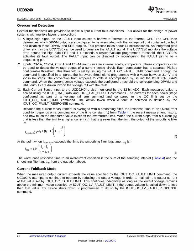
Because the current measurement is averaged with a smoothing filter, the response time to an Overcurrentcondition depends on a combination of the time constant (τ) from Table 4, the recent measurement history,and how much the measured value exceeds the overcurrent limit. When the current steps from a current (I1)that is less than the limit to a higher current (I2) that is greater than the limit, the output of the smoothing filteris:
At the point when Ismoothed exceeds the limit, the smoothing filter lags time, tlag is:
The worst case response time to an overcurrent condition is the sum of the sampling interval (Table 4) and thesmoothing filter lag, tlag from the equation above.
When the measured output current exceeds the value specified by the IOUT_OC_FAULT_LIMIT command, theUCD9240 attempts to continue to operate by reducing the output voltage in order to maintain the output currentat the value set by IOUT_OC_FAULT_LIMIT. This continues indefinitely as long as the output voltage remainsabove the minimum value specified by IOUT_OC_LV_FAULT_LIMIT. If the output voltage is pulled down to lessthan that value, the device shuts down, if programmed to do so by the IOUT_OC_LV_FAULT_RESPONSEcommand.
22 Submit Documentation Feedback Copyright © 2008, Texas Instruments Incorporated
Product Folder Link(s): UCD9240
Input Voltage and Current Monitoring
Temperature Monitoring
CD74HC4051
Temp-rail1A
Temp-rail1B
Temp-rail2A
Temp-rail2B
Temp-rail3A
Temp-rail4A
13
14
15
12
1
5
2
4
+3.3V
Com
S2
S1
S0
-EN
A0
A1
A2
A3
A4
A5
A6
A7
Temp
TMUX2
TMUX1
TMUX0
3
9
10
11
6
16
8
UCD9240
www.ti.com ................................................................................................................................................... SLUS766C–JULY 2008–REVISED NOVEMBER 2008
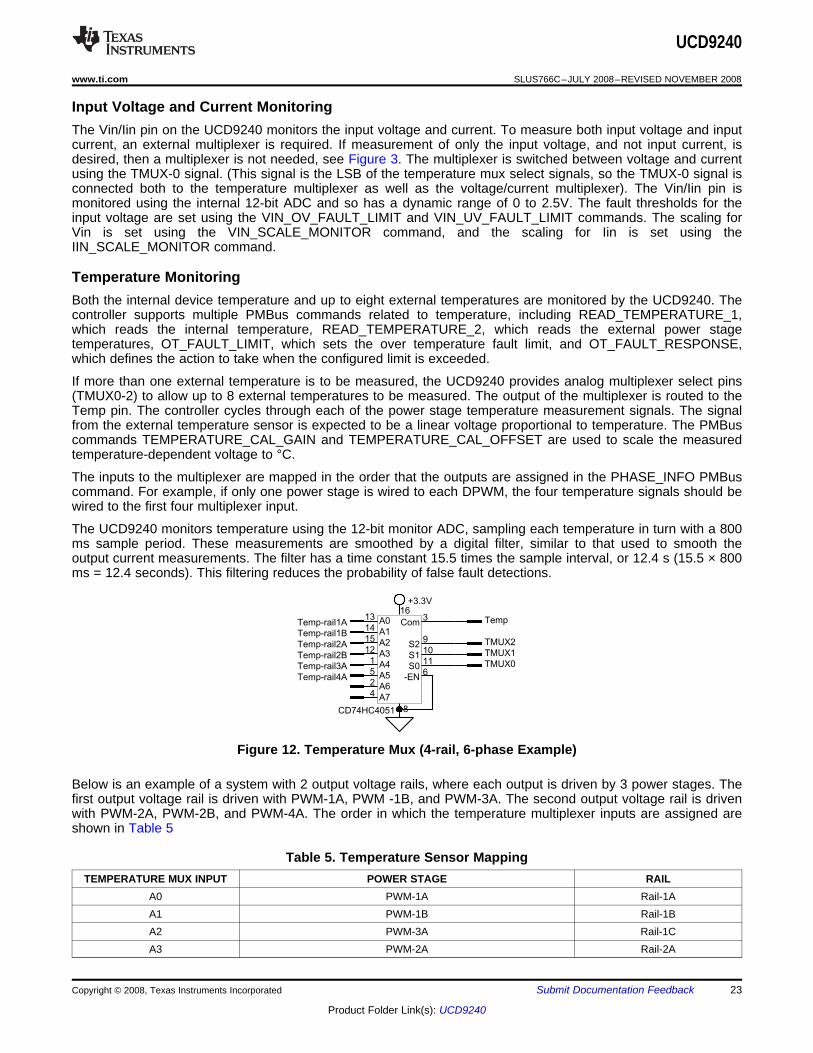
The Vin/Iin pin on the UCD9240 monitors the input voltage and current. To measure both input voltage and inputcurrent, an external multiplexer is required. If measurement of only the input voltage, and not input current, isdesired, then a multiplexer is not needed, see Figure 3. The multiplexer is switched between voltage and currentusing the TMUX-0 signal. (This signal is the LSB of the temperature mux select signals, so the TMUX-0 signal isconnected both to the temperature multiplexer as well as the voltage/current multiplexer). The Vin/Iin pin ismonitored using the internal 12-bit ADC and so has a dynamic range of 0 to 2.5V. The fault thresholds for theinput voltage are set using the VIN_OV_FAULT_LIMIT and VIN_UV_FAULT_LIMIT commands. The scaling forVin is set using the VIN_SCALE_MONITOR command, and the scaling for Iin is set using theIIN_SCALE_MONITOR command.
Both the internal device temperature and up to eight external temperatures are monitored by the UCD9240. Thecontroller supports multiple PMBus commands related to temperature, including READ_TEMPERATURE_1,which reads the internal temperature, READ_TEMPERATURE_2, which reads the external power stagetemperatures, OT_FAULT_LIMIT, which sets the over temperature fault limit, and OT_FAULT_RESPONSE,which defines the action to take when the configured limit is exceeded.
If more than one external temperature is to be measured, the UCD9240 provides analog multiplexer select pins(TMUX0-2) to allow up to 8 external temperatures to be measured. The output of the multiplexer is routed to theTemp pin. The controller cycles through each of the power stage temperature measurement signals. The signalfrom the external temperature sensor is expected to be a linear voltage proportional to temperature. The PMBuscommands TEMPERATURE_CAL_GAIN and TEMPERATURE_CAL_OFFSET are used to scale the measuredtemperature-dependent voltage to °C.
The inputs to the multiplexer are mapped in the order that the outputs are assigned in the PHASE_INFO PMBuscommand. For example, if only one power stage is wired to each DPWM, the four temperature signals should bewired to the first four multiplexer input.
The UCD9240 monitors temperature using the 12-bit monitor ADC, sampling each temperature in turn with a 800ms sample period. These measurements are smoothed by a digital filter, similar to that used to smooth theoutput current measurements. The filter has a time constant 15.5 times the sample interval, or 12.4 s (15.5 × 800ms = 12.4 seconds). This filtering reduces the probability of false fault detections.
Figure 12. Temperature Mux (4-rail, 6-phase Example)
Below is an example of a system with 2 output voltage rails, where each output is driven by 3 power stages. Thefirst output voltage rail is driven with PWM-1A, PWM -1B, and PWM-3A. The second output voltage rail is drivenwith PWM-2A, PWM-2B, and PWM-4A. The order in which the temperature multiplexer inputs are assigned areshown in Table 5
Table 5. Temperature Sensor MappingTEMPERATURE MUX INPUT POWER STAGE RAIL
A0 PWM-1A Rail-1AA1 PWM-1B Rail-1BA2 PWM-3A Rail-1CA3 PWM-2A Rail-2A
Copyright © 2008, Texas Instruments Incorporated Submit Documentation Feedback 23
Product Folder Link(s): UCD9240
Temperature Balancing
Soft Start, Soft Stop Ramp Sequence
2 4 6 8 10 14 16120–0.2
0
0.2
0.4
0.6
0.8
1.0
1.2
Time ms
Start into a pre-bias
Start from zero
2 4 6 8 10 14 16120–0.2
0
0.2
0.4
0.6
0.8
1.0
1.2
Time ms
Bridged, 0.45-V bias
Unbridged,
no bias
Unbridged,
0.45-V bias
Soft-Start Soft-Stop
Vo
lts
Vo
lts
PWM begins here from 0 output voltage
PWM begins here with pre-bias
UCD9240
SLUS766C–JULY 2008–REVISED NOVEMBER 2008................................................................................................................................................... www.ti.com
Table 5. Temperature Sensor Mapping (continued)TEMPERATURE MUX INPUT POWER STAGE RAIL
A4 PWM-2B Rail-2BA5 PWM-4A Rail-2CA6 - -A7 - -
Temperature balancing between phases is performed by adjusting the current such that cooler phases draw alarger share of the current. Temperature balancing occurs slowly (the loop runs at a 10 Hz rate), and only whenthe phase currents exceeds the PMBus settable TEMP_BALANCE_IMIN. This minimum current thresholdprevents the controller from "winding up" and forcing one phase to carry all the current under a low-loadcondition, when the total current may be insufficient to significantly affect phase temperatures.
The UCD9240 performs soft start and soft stop ramps under closed loop control. Performing a start or stop rampor tracking is considered a separate operational mode. The other operational modes are normal regulation andlight load regulation. Each operational mode can be configured to have an independent loop gain andcompensation. Each set of loop gain coefficients is called a "bank" and is configured using the CLA_GAINSPMBus command.
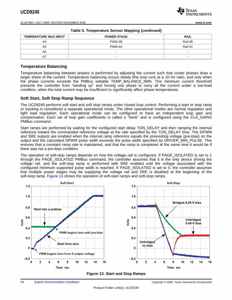
Start ramps are performed by waiting for the configured start delay TON_DELAY and then ramping the internalreference toward the commanded reference voltage at the rate specified by the TON_DELAY time. The DPWMand SRE outputs are enabled when the internal ramp reference equals the preexisting voltage (pre-bias) on theoutput and the calculated DPWM pulse width exceeds the pulse width specified by DRIVER_MIN_PULSE. Thisensures that a constant ramp rate is maintained, and that the ramp is completed at the same time it would be ifthere was not a pre-bias condition.
The operation of soft-stop ramps depends on how the voltage rail is configured. If PAGE_ISOLATED is set to 1through the PAGE_ISOLATED PMBus command, the controller assumes that it is the only device driving thevoltage rail, and the soft-stop ramp is performed with SRE enabled until the voltage associated with theconfigured minimum supported pulse width is reached. If PAGE_ISOLATED is set to 0, the controller assumesthat multiple power stages may be supplying the voltage rail and SRE is disabled at the beginning of thesoft-stop ramp. Figure 13 shows the operation of soft-start ramps and soft-stop ramps.
Figure 13. Start and Stop Ramps
24 Submit Documentation Feedback Copyright © 2008, Texas Instruments Incorporated
Product Folder Link(s): UCD9240
Input UV Lockout
Voltage Tracking
UCD9240
www.ti.com ................................................................................................................................................... SLUS766C–JULY 2008–REVISED NOVEMBER 2008
When a voltage rail is in its idle state, the DPWM and SRE outputs are disabled, and the differential voltage onthe EAP/EAN pins are monitored by the controller. During idle the setpoint DAC is adjusted to minimize the errorvoltage. If there is a pre-bias (that is, a non-zero voltage on the regulated output), then the device can begin thestart ramp from that voltage with a minimum of disturbance. This is done by calculating the duty cycle that isrequired to match the measured voltage on the rail. Nominally this is calculated as Vin / Vout; however, to allowfor losses and offsets in the system, PREBIAS_GAIN and PREBIAS_OFFSET can be used for fine tuning. If thepre-bias voltage on the output requires a smaller pulse width than the driver can deliver, as defined by theDRIVER_MIN_PULSE PMBus command, then the start ramp is delayed until the internal ramp reference voltagehas increased to the point where the required duty cycle exceeds the specified minimum duty.
Once a soft start/stop ramp has begun, the output is controlled by adjusting the setpoint DAC at a fixed rate andallowing the digital compensator control engine to generate a duty cycle based on the error. The setpoint DACadjustments are made at a rate of 10 kHz and are based on the TON_RISE or TOFF_FALL PMBus configurationparameters.
Although the presence of a pre-bias voltage or a specified minimum DPWM pulse width affects the time whenthe DPWM and SRE signals become active, the time from when the controller starts processing the turn-oncommand to the time when it reaches regulation is TON_DELAY plus TON_RISE, regardless of the pre-bias orminimum duty cycle.
During a normal ramp (i.e. no tracking, no current limiting events and no EADC saturation), the setpoint slews ata pre-calculated rate based on the commanded output voltage and TON_RISE. Under closed loop control, thecompensator follows this ramp up to the regulation point.
Because the EADC in the controller has a limited range, it may saturate due to a large transient during astart/stop ramp. If this occurs, the controller overrides the calculated setpoint ramp value, and adjusts thereference DAC in the direction to minimize the error. It continues to step the reference DAC in this direction untilthe EADC comes out of saturation. Once it is out of saturation, the start ramp continues, but from this newsetpoint voltage; and therefore, has an impact on the ramp time.
The normal operation supply lock-out voltage thresholds are configured with the VIN_ON and VIN_OFFcommands. When input supply voltage drops below the value set by VIN_OFF, the device starts a normal softstop ramp. When the input supply voltage drops below the voltage set by VIN_UV_FAULT_LIMIT, the deviceperforms per the configuration using the VIN_UV_FAULT_RESPONSE command. For example, when the biassupply for the controller is derived from another source, the response code can be set to "Continue" or "Continuewith delay," and the controller attempts to finish the soft stop ramp. If the bias voltages for the controller and gatedriver are uncertain below some voltage, the user can set the UV fault limit to that voltage and specify theresponse code to be "shut down immediately" disabling all DPWM and SRE outputs. If VIN_OFF sets the voltageat which the output voltage soft-stop ramp is initiated, and VIN_UV_FAULT_LIMIT sets the voltage where powerconversion is stopped.
Each voltage rail can be configured to operate in a tracking mode. When a voltage rail is configured to trackanother voltage rail, it adjusts the setpoint to follow the master, which can be either another internal rail or theexternal Vtrack pin. As in standard non-tracking mode, a target Vout is still specified for the voltage rail. If thetracking input exceeds this target, the tracking voltage rail stops following the master signal, switch to regulationgains, and regulate at the target voltage. When the tracking input drops back below the target (with 20 mV ofhysteresis), tracking gains is re-loaded, and the voltage rail follows the tracking reference. Note that the targetcan be set above the range of the tracking input, forcing the voltage rail to always remain in tracking mode.
During tracking, the setpoint DAC is permitted to change only as fast as is possible without inducing the EADC tosaturate. This limit may be reached if the master ramps at an extremely fast rate, or if the master is at asignificantly different voltage when the rail is turned on. As in normal regulation, a current limit (current foldback)or the detection of the EADC saturating forces the rail to temporarily deviate from the tracking reference.
The PMBus command TRACKING_SOURCE is available to enable tracking mode and select the master to track.The tracking mode is set individually for each rail, allowing each rail to have a different master, multiple rails toshare a master, or some rails to track while others remain independent. Additionally,TRACKING_SCALE_MONITOR permits tracking at voltage with a fixed ratio to a master voltage. For example, aratio of 0.5 causes the rail to regulate at one half of the master’s voltage.
Copyright © 2008, Texas Instruments Incorporated Submit Documentation Feedback 25
Product Folder Link(s): UCD9240
Sequencing
UCD9240
SLUS766C–JULY 2008–REVISED NOVEMBER 2008................................................................................................................................................... www.ti.com
There are three methods to squence voltage rails controlled by the UCD9240 that allow for a variety of systemsequencing configurations. Each of these options is configurable in the GUI. These methods include:1. Use the PMBus to set the soft start/stop parameters for each rail. Multiple start/stop sequences may be
triggered simultaneously. Each voltage rail performs its sequencing in an open-loop manner. If any rail failsto complete its sequence, all other rails are unaffected.
2. Daisy-chain the Power Good output signal from one controller to the PMBus-CTRL input on another.3. Use the GPIO_SEQ_CONFIG command to assign dependencies between rails, or to configure unused pins
as sequencing control inputs or sequencing status outputs.
Method 1: Each rail has programmable delay times, TON_DELAY and TOFF_DELAY, before beginning a softstart ramp or a soft stop ramp, and programmable ramp times, TON_RISE and TOFF_FALL determine how longthe ramp takes. These PMBus commands are defined in the UCD92xx PMBUS Command Reference. Theparameters can also be configured using the Fusion Digital Power™ Designer GUI (seehttp://focus.ti.com/docs/toolsw/folders/print/fusion_digital_power_designer.html). The configurable times can beused to program a time based sequence for each voltage rail. Using this method each rail ramps independentlyand completes the ramp regardless of the success of the other rails.
The start/stop sequence is initiated for a single rail by the PMBus-CTRL pin or via the PMBus using theOPERATION or ON_OFF_CONTROL commands.
The start/stop sequence may be initiated simultaneously for multiple rails within the same controller byconfiguring each rail to respond to the PMBus-CTRL pin. Alternatively, after setting the PMBus PAGE variable to255, subsequent OPERATION or ON_OFF_CONTROL commands applies to all rails at the same time.
To simultaneously initiate start/stop sequences in multiple controllers, a common PMBus-CTRL signal can be fedinto each controller. Alternatively, the PMBus Group Command Protocol may be used to send separatecommands to multiple controllers. All the commands are sent in one continuous transmission and wait for thefinal STOP signal in order to start executing their commands simultaneously.
Method 2: The Power Good pin can be used to coordinate multiple controllers by running the Power Good pinoutput from one controller to the PMBus-CTRL input pin of another. This imposes a master/slave relationshipbetween multiple devices. During startup, the slave controllers initiates their start sequences after the mastercompletes its start sequence and reaches its regulation voltage. During shut-down, as soon as the master startsits shut-down sequence, the shut-down signals to its slaves.
Unlike Method 1, a shut-down on one or more rails on the master can initiate shut-downs of the slave devices.The master shut-downs can initiate intentionally or by a fault condition.
The PMBus specification implies that the Power Good signal is active when ALL the rails in a controller areabove their power-good “on” threshold setting. The UCD9240 allows the Power Good pin to be reprogrammedusing the GPIO_SEQ_CONFIG command so that the pin responds to a desired subset of rails.
This method works to coordinate multiple controllers, but it does not enforce interdependency between railswithin a single controller.
Method 3: Using the GPIO_SEQ_CONFIG command, several sequencing options can be configured usingundedicated pins for input/output. As many as four pins can be configured as inputs, and as many as eight asoutputs. The outputs can be open-drain or actively driven with selectable polarity.
Each rail can be configured to respond to a combination of the power-good status of other internal rails and/orthe state of sequencing input pins. The output pins can be configured to reflect the power-good status of acombination of rails, or to one of several status indicators including power-good, an Overcurrent warning, or the“open-drain outputs valid” signal.
When using the output signals for sequencing, they may be routed to sequencing control inputs or to thePMBus-CTRL inputs on other controllers.
Once each rail’s input dependencies are configured, the rail responds to those input pins or internal rails. Likemethod 2, shut-downs on one rail or controller can initiate shut-downs of other rails or controllers. Unlike method2, GPIO_SEQ_CONFIG offers much more flexibility in assigning relationships between multiple rails within asingle controller or between multiple controllers. It is possible for each controller to be both a master and a slaveto another controller.
26 Submit Documentation Feedback Copyright © 2008, Texas Instruments Incorporated
Product Folder Link(s): UCD9240
UCD9240
www.ti.com ................................................................................................................................................... SLUS766C–JULY 2008–REVISED NOVEMBER 2008
GPIO_SEQ_CONFIG allows the configuration of fault relationships such that a fault on one rail can result in theshut down of any selection of rails in addition to the rail at fault. These fault interactions are not constrained to asingle master/slave relationship; for example, a system can be configured such that a fault on any rail shutsdown all rails. If the fault response of the failing rail is to shut down immediately, all dependent rails follow suitand shuts down immediately regardless of their programmed response code.
Each rail can be optionally configured to monitor a sequencing input pin for a specified period of time after itturns on and reaches its power good threshold. If the programmable timeout is reached before the input pin statematches its defined logic level, the rail is shut down, and a status error posted. This feature could be used, forexample, to ensure that an LDO on the board did turn on when the main system voltage came up. Each rail isenabled independently of the other rails and has a unique timeout value; a single input pin is used as the timeoutsource.
The setup of the GPIO_SEQ_CONFIG command is aided by the use of the Fusion Digital Power™ Designer,which graphically displays relationships between rails and provides intuitive controls to allocate and configureavailable resources.
The following pins are available for use as GPIO or sequencing control, provided they are not being used fortheir primary purpose:
PIN NAME 80-PIN 64-PINDPWM-1A IN/OUT IN/OUTDPWM-1B IN/OUT IN/OUTDPWM-2A IN/OUT IN/OUTDPWM-2B IN/OUT IN/OUTDPWM-3A IN/OUT IN/OUTDPWM-3B IN/OUT –DPWM-4A IN/OUT IN/OUTDPWM-4B IN/OUT –
FAULT-1A IN/OUT IN/OUTFAULT-1B IN/OUT IN/OUTFAULT-2A IN/OUT IN/OUTFAULT-2B IN/OUT IN/OUTFAULT-3A IN/OUT IN/OUTFAULT-3B IN/OUT –FAULT-4A IN/OUT IN/OUTFAULT-4B IN/OUT –
SRE-1A IN/OUT IN/OUTSRE-1B IN/OUT IN/OUTSRE-2A IN/OUT IN/OUTSRE-2B IN/OUT IN/OUTSRE-3A IN/OUT IN/OUTSRE-3B IN/OUT –SRE-4A IN/OUT IN/OUTSRE-4B IN/OUT –POWER_GOOD IN/OUT IN/OUTFAN_TACH IN/OUT IN/OUTFAN_PWM IN (1) IN (1)
DIAG_LED IN (1) –
(1) The FAN_PWM and Diag_LED pins are outputs when configured for their primary purpose. Whenconfigured for sequencing, they may be used only as inputs.
Copyright © 2008, Texas Instruments Incorporated Submit Documentation Feedback 27
Product Folder Link(s): UCD9240

Fan Control
+
1k31k0
1u
FAN-PWM
FAN-TACH
12V
FAN
33k2
0.1u
TIP31A
TS321
10k0
3.3V
Non-volatile Memory Error Correction Coding
APPLICATION INFORMATION
Calculation of Open Loop Gain Using the UCD9240
UCD9240
SLUS766C–JULY 2008–REVISED NOVEMBER 2008................................................................................................................................................... www.ti.com
The UCD9240 can control one fan as defined in the PMBus standard. When enabled, the FAN-PWM controloutput provides a 156 kHz digital signal, with a duty cycle that is set based on the FAN_COMMAND_1 PMBuscommand. The duty cycle can be set from 0% to 100% with 1% resolution.
The FAN-TACH input counts the number of transitions in the tachometer output from the fan in each 1 secondinterval. The fan speed may be read by issuing the READ_FAN_SPEED_1 command. The speed is returned inRPMs.
Different fans may output from one to four tachometer pulses per revolution. The FAN_CONFIG_1_2 commandis used to set the number of tachometer pulses per revolution. The same command is used to indicate whether afan is attached.
The UCD9240 can report fan speed faults when the fan speed is too slow for 5 consecutive seconds. The fanspeed fault limit is set by the FAN_SPEED_FAULT_LIMIT command. The status is checked by issuing theSTATUS_FAN_1_2 command. See the UCD92xx PMBUS Command Reference for a complete description ofeach command.
Figure 14. Example Fan Control Circuit
The UCD9240 uses Error Correcting Code (ECC) to improve data integrity and provide high reliability storage ofData Flash contents. ECC uses dedicated hardware to generate extra check bits for the user data as it is writteninto the Flash memory. This adds an additional six bits to each 32-bit memory word stored into the Flash array.These extra check bits, along with the hardware ECC algorithm, allow for any single bit error to be detected andcorrected when the Data Flash is read.
When designing a power supply it is necessary to determine the stability of the closed loop system. The usualway to do this is to determine the open loop gain versus frequency and from the open loop gain determine thegain margin and phase margin. Figure 15 shows a block diagram of a complete control loop using the UDC9240.Each component of the loop gain that is a function of frequency is labeled "Gx". Constant gain components arelabeled "Kx".
CONSTANT GAIN COMPONENTS DESCRIPTIONTransfer function for the power stage circuit consisting of the FET switches, LC output filterGplant and load.
Gdiv Transfer function for the VOUT sense divider and its capacitive filter network.KAFE Analog fron-end amplifier gain.
KEADC Gain of the 6-bit EADC in units of LSBs/V
28 Submit Documentation Feedback Copyright © 2008, Texas Instruments Incorporated
Product Folder Link(s): UCD9240

Power Stage
Gplant(f)Gdiv(f)
KAFEKEADCKnonlinearGCLA2GCLA1
KPWM +
Vout
Vin
Gdelay
VrefDAC
divider
UCD9240CPU
PMBus
Automatic System Identification (Auto-ID™)
EAp/EAn Voltage Sense Filtering
UCD9240
www.ti.com ................................................................................................................................................... SLUS766C–JULY 2008–REVISED NOVEMBER 2008
CONSTANT GAIN COMPONENTS DESCRIPTIONGdelay Phase shift due to the delays in the control loop.
Knonlinear Nonlinear function gain. Gain for the limit interval that contains zero error.GCLA2 Transfer function of the second order filter section of the compensator.GCLA1 Transfer function of the first order filter section of the compensator.KPWM Accounts for the bit resolution of the input to the DPWM
Figure 15. Loop Gain Contributions
Several of the gain blocks are programmable. They are configured by issuing a CLA_GAINS command over thePMBus. The syntax for this command is shown in the UCD92xx PMBUS Command Reference. These gains canalso be configured using the Fusion Digital Power™ Designer PC program.
By using digital circuits to create the control function for a switch-mode power supply, additional features can beimplemented. One of those features is the measurement of the open loop gain and stability margin of the powersupply without the use of external test equipment. This capability is called automatic system identification orAuto-ID™. To identify the frequency response, the UCD9240 internally synthesizes a sine wave signal andinjects it into the loop at the set point DAC. This signal excites the system, and the closed-loop response to thatexcitation can be measured at another point in the loop. The UCD9240 measures the response to the excitationat the output of the digital compensator. From the closed-loop response, the open-loop transfer function iscalculated. The open-loop transfer function may be calculated from the closed-loop response.
Note that since the compensator and DPWM are digital, their transfer functions are known exactly and can bedivided out of the measured open-loop gain. In this way the UCD9240 can accurately measure the powerstage/load plant transfer function in situ (in place), on the factory floor or in an end equipment application andsend the measurement data back to a host through the PMBus interface without the need for external testequipment. Details of the Auto-ID™ PMBus measurement commands can be found in the UCD92xx PMBusCommand Reference.
Conditioning should be provided on the EAp and EAn signals. Figure 16 shows a divider network between theoutput voltage and the voltage sense input to the controller. The resistor divider is used to bring the outputvoltage within the dynamic range of the controller. When no attenuation is needed, R2 can be left open and thesignal conditioned by the low-pass filter formed by R1 and C2.
Copyright © 2008, Texas Instruments Incorporated Submit Documentation Feedback 29
Product Folder Link(s): UCD9240
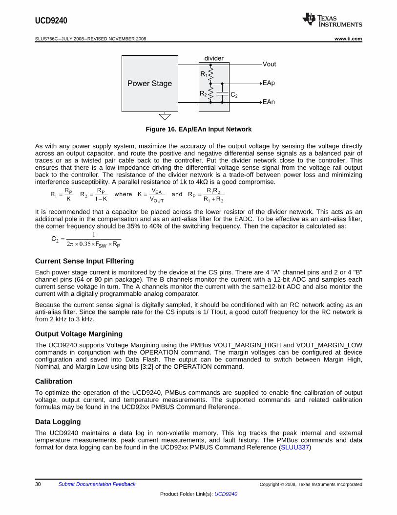
Power Stage
Voutdivider
R1
R2 C2
EAn
EAp
1 2
1 2
1 21
= = = =
- +
P P EAP
OUT
R R V R RR R where K and R
K K V R R
2
1
2 0.35p
=
´ ´ ´SW P
CF R
Current Sense Input FIltering
Output Voltage Margining
Calibration
Data Logging
UCD9240
SLUS766C–JULY 2008–REVISED NOVEMBER 2008................................................................................................................................................... www.ti.com
Figure 16. EAp/EAn Input Network
As with any power supply system, maximize the accuracy of the output voltage by sensing the voltage directlyacross an output capacitor, and route the positive and negative differential sense signals as a balanced pair oftraces or as a twisted pair cable back to the controller. Put the divider network close to the controller. Thisensures that there is a low impedance driving the differential voltage sense signal from the voltage rail outputback to the controller. The resistance of the divider network is a trade-off between power loss and minimizinginterference susceptibility. A parallel resistance of 1k to 4kΩ is a good compromise.
It is recommended that a capacitor be placed across the lower resistor of the divider network. This acts as anadditional pole in the compensation and as an anti-alias filter for the EADC. To be effective as an anti-alias filter,the corner frequency should be 35% to 40% of the switching frequency. Then the capacitor is calculated as:
Each power stage current is monitored by the device at the CS pins. There are 4 "A" channel pins and 2 or 4 "B"channel pins (64 or 80 pin package). The B channels monitor the current with a 12-bit ADC and samples eachcurrent sense voltage in turn. The A channels monitor the current with the same12-bit ADC and also monitor thecurrent with a digitally programmable analog comparator.
Because the current sense signal is digitally sampled, it should be conditioned with an RC network acting as ananti-alias filter. Since the sample rate for the CS inputs is 1/ TIout, a good cutoff frequency for the RC network isfrom 2 kHz to 3 kHz.
The UCD9240 supports Voltage Margining using the PMBus VOUT_MARGIN_HIGH and VOUT_MARGIN_LOWcommands in conjunction with the OPERATION command. The margin voltages can be configured at deviceconfiguration and saved into Data Flash. The output can be commanded to switch between Margin High,Nominal, and Margin Low using bits [3:2] of the OPERATION command.
To optimize the operation of the UCD9240, PMBus commands are supplied to enable fine calibration of outputvoltage, output current, and temperature measurements. The supported commands and related calibrationformulas may be found in the UCD92xx PMBUS Command Reference.
The UCD9240 maintains a data log in non-volatile memory. This log tracks the peak internal and externaltemperature measurements, peak current measurements, and fault history. The PMBus commands and dataformat for data logging can be found in the UCD92xx PMBUS Command Reference (SLUU337)
30 Submit Documentation Feedback Copyright © 2008, Texas Instruments Incorporated
Product Folder Link(s): UCD9240
PACKAGE OPTION ADDENDUM
www.ti.com 15-Apr-2017
Addendum-Page 1
PACKAGING INFORMATION
Orderable Device Status(1)
Package Type PackageDrawing
Pins PackageQty
Eco Plan(2)
Lead/Ball Finish(6)
MSL Peak Temp(3)
Op Temp (°C) Device Marking(4/5)
Samples
HPA00589RGCR NRND VQFN RGC 64 2000 Green (RoHS& no Sb/Br)
CU NIPDAU Level-3-260C-168 HR -40 to 125 UCD9240
HPA00589RGCT NRND VQFN RGC 64 250 Green (RoHS& no Sb/Br)
CU NIPDAU Level-3-260C-168 HR -40 to 125 UCD9240
UCD9240PFC NRND TQFP PFC 80 96 Green (RoHS& no Sb/Br)
CU NIPDAU Level-2-260C-1 YEAR -40 to 125 UCD9240
UCD9240PFCG4 NRND TQFP PFC 80 96 Green (RoHS& no Sb/Br)
CU NIPDAU Level-2-260C-1 YEAR -40 to 125 UCD9240
UCD9240PFCR NRND TQFP PFC 80 1000 Green (RoHS& no Sb/Br)
CU NIPDAU Level-2-260C-1 YEAR -40 to 125 UCD9240
UCD9240RGCR NRND VQFN RGC 64 2000 Green (RoHS& no Sb/Br)
CU NIPDAU Level-3-260C-168 HR -40 to 125 UCD9240
UCD9240RGCT NRND VQFN RGC 64 250 Green (RoHS& no Sb/Br)
CU NIPDAU Level-3-260C-168 HR -40 to 125 UCD9240
(1) The marketing status values are defined as follows:ACTIVE: Product device recommended for new designs.LIFEBUY: TI has announced that the device will be discontinued, and a lifetime-buy period is in effect.NRND: Not recommended for new designs. Device is in production to support existing customers, but TI does not recommend using this part in a new design.PREVIEW: Device has been announced but is not in production. Samples may or may not be available.OBSOLETE: TI has discontinued the production of the device.
(2) Eco Plan - The planned eco-friendly classification: Pb-Free (RoHS), Pb-Free (RoHS Exempt), or Green (RoHS & no Sb/Br) - please check http://www.ti.com/productcontent for the latest availabilityinformation and additional product content details.TBD: The Pb-Free/Green conversion plan has not been defined.Pb-Free (RoHS): TI's terms "Lead-Free" or "Pb-Free" mean semiconductor products that are compatible with the current RoHS requirements for all 6 substances, including the requirement thatlead not exceed 0.1% by weight in homogeneous materials. Where designed to be soldered at high temperatures, TI Pb-Free products are suitable for use in specified lead-free processes.Pb-Free (RoHS Exempt): This component has a RoHS exemption for either 1) lead-based flip-chip solder bumps used between the die and package, or 2) lead-based die adhesive used betweenthe die and leadframe. The component is otherwise considered Pb-Free (RoHS compatible) as defined above.Green (RoHS & no Sb/Br): TI defines "Green" to mean Pb-Free (RoHS compatible), and free of Bromine (Br) and Antimony (Sb) based flame retardants (Br or Sb do not exceed 0.1% by weightin homogeneous material)
(3) MSL, Peak Temp. - The Moisture Sensitivity Level rating according to the JEDEC industry standard classifications, and peak solder temperature.
(4) There may be additional marking, which relates to the logo, the lot trace code information, or the environmental category on the device.

PACKAGE OPTION ADDENDUM
www.ti.com 15-Apr-2017
Addendum-Page 2
(5) Multiple Device Markings will be inside parentheses. Only one Device Marking contained in parentheses and separated by a "~" will appear on a device. If a line is indented then it is a continuationof the previous line and the two combined represent the entire Device Marking for that device.
(6) Lead/Ball Finish - Orderable Devices may have multiple material finish options. Finish options are separated by a vertical ruled line. Lead/Ball Finish values may wrap to two lines if the finishvalue exceeds the maximum column width.
Important Information and Disclaimer:The information provided on this page represents TI's knowledge and belief as of the date that it is provided. TI bases its knowledge and belief on informationprovided by third parties, and makes no representation or warranty as to the accuracy of such information. Efforts are underway to better integrate information from third parties. TI has taken andcontinues to take reasonable steps to provide representative and accurate information but may not have conducted destructive testing or chemical analysis on incoming materials and chemicals.TI and TI suppliers consider certain information to be proprietary, and thus CAS numbers and other limited information may not be available for release.
In no event shall TI's liability arising out of such information exceed the total purchase price of the TI part(s) at issue in this document sold by TI to Customer on an annual basis.

TAPE AND REEL INFORMATION
*All dimensions are nominal
Device PackageType
PackageDrawing
Pins SPQ ReelDiameter
(mm)
ReelWidth
W1 (mm)
A0(mm)
B0(mm)
K0(mm)
P1(mm)
W(mm)
Pin1Quadrant
UCD9240PFCR TQFP PFC 80 1000 330.0 24.4 15.0 15.0 1.5 20.0 24.0 Q2
UCD9240RGCR VQFN RGC 64 2000 330.0 16.4 9.3 9.3 1.1 12.0 16.0 Q2
UCD9240RGCT VQFN RGC 64 250 180.0 16.4 9.3 9.3 1.1 12.0 16.0 Q2
UCD9240RGCT VQFN RGC 64 250 180.0 16.4 9.3 9.3 1.5 12.0 16.0 Q2
PACKAGE MATERIALS INFORMATION
www.ti.com 11-Apr-2015
Pack Materials-Page 1

*All dimensions are nominal
Device Package Type Package Drawing Pins SPQ Length (mm) Width (mm) Height (mm)
UCD9240PFCR TQFP PFC 80 1000 367.0 367.0 45.0
UCD9240RGCR VQFN RGC 64 2000 367.0 367.0 38.0
UCD9240RGCT VQFN RGC 64 250 210.0 185.0 35.0
UCD9240RGCT VQFN RGC 64 250 210.0 185.0 35.0
PACKAGE MATERIALS INFORMATION
www.ti.com 11-Apr-2015
Pack Materials-Page 2

MECHANICAL DATA
MTQF009A – OCTOBER 1994 – REVISED DECEMBER 1996
POST OFFICE BOX 655303 • DALLAS, TEXAS 75265
PFC (S-PQFP-G80) PLASTIC QUAD FLATPACK
4073177/B 11/96
40
210,13 NOM
0,25
0,750,45
Seating Plane
0,05 MIN
Gage Plane
0,27
41
0,17
20
60
1
61
80
SQ
SQ
12,20
13,8014,20
11,80
9,50 TYP
1,05
1,20 MAX
0,95
0,08
0,50 M0,08
0°–7°
NOTES: A. All linear dimensions are in millimeters.B. This drawing is subject to change without notice.C. Falls within JEDEC MS-026
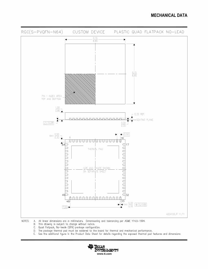

IMPORTANT NOTICE
Texas Instruments Incorporated (TI) reserves the right to make corrections, enhancements, improvements and other changes to itssemiconductor products and services per JESD46, latest issue, and to discontinue any product or service per JESD48, latest issue. Buyersshould obtain the latest relevant information before placing orders and should verify that such information is current and complete.TI’s published terms of sale for semiconductor products (http://www.ti.com/sc/docs/stdterms.htm) apply to the sale of packaged integratedcircuit products that TI has qualified and released to market. Additional terms may apply to the use or sale of other types of TI products andservices.Reproduction of significant portions of TI information in TI data sheets is permissible only if reproduction is without alteration and isaccompanied by all associated warranties, conditions, limitations, and notices. TI is not responsible or liable for such reproduceddocumentation. Information of third parties may be subject to additional restrictions. Resale of TI products or services with statementsdifferent from or beyond the parameters stated by TI for that product or service voids all express and any implied warranties for theassociated TI product or service and is an unfair and deceptive business practice. TI is not responsible or liable for any such statements.Buyers and others who are developing systems that incorporate TI products (collectively, “Designers”) understand and agree that Designersremain responsible for using their independent analysis, evaluation and judgment in designing their applications and that Designers havefull and exclusive responsibility to assure the safety of Designers' applications and compliance of their applications (and of all TI productsused in or for Designers’ applications) with all applicable regulations, laws and other applicable requirements. Designer represents that, withrespect to their applications, Designer has all the necessary expertise to create and implement safeguards that (1) anticipate dangerousconsequences of failures, (2) monitor failures and their consequences, and (3) lessen the likelihood of failures that might cause harm andtake appropriate actions. Designer agrees that prior to using or distributing any applications that include TI products, Designer willthoroughly test such applications and the functionality of such TI products as used in such applications.TI’s provision of technical, application or other design advice, quality characterization, reliability data or other services or information,including, but not limited to, reference designs and materials relating to evaluation modules, (collectively, “TI Resources”) are intended toassist designers who are developing applications that incorporate TI products; by downloading, accessing or using TI Resources in anyway, Designer (individually or, if Designer is acting on behalf of a company, Designer’s company) agrees to use any particular TI Resourcesolely for this purpose and subject to the terms of this Notice.TI’s provision of TI Resources does not expand or otherwise alter TI’s applicable published warranties or warranty disclaimers for TIproducts, and no additional obligations or liabilities arise from TI providing such TI Resources. TI reserves the right to make corrections,enhancements, improvements and other changes to its TI Resources. TI has not conducted any testing other than that specificallydescribed in the published documentation for a particular TI Resource.Designer is authorized to use, copy and modify any individual TI Resource only in connection with the development of applications thatinclude the TI product(s) identified in such TI Resource. NO OTHER LICENSE, EXPRESS OR IMPLIED, BY ESTOPPEL OR OTHERWISETO ANY OTHER TI INTELLECTUAL PROPERTY RIGHT, AND NO LICENSE TO ANY TECHNOLOGY OR INTELLECTUAL PROPERTYRIGHT OF TI OR ANY THIRD PARTY IS GRANTED HEREIN, including but not limited to any patent right, copyright, mask work right, orother intellectual property right relating to any combination, machine, or process in which TI products or services are used. Informationregarding or referencing third-party products or services does not constitute a license to use such products or services, or a warranty orendorsement thereof. Use of TI Resources may require a license from a third party under the patents or other intellectual property of thethird party, or a license from TI under the patents or other intellectual property of TI.TI RESOURCES ARE PROVIDED “AS IS” AND WITH ALL FAULTS. TI DISCLAIMS ALL OTHER WARRANTIES ORREPRESENTATIONS, EXPRESS OR IMPLIED, REGARDING RESOURCES OR USE THEREOF, INCLUDING BUT NOT LIMITED TOACCURACY OR COMPLETENESS, TITLE, ANY EPIDEMIC FAILURE WARRANTY AND ANY IMPLIED WARRANTIES OFMERCHANTABILITY, FITNESS FOR A PARTICULAR PURPOSE, AND NON-INFRINGEMENT OF ANY THIRD PARTY INTELLECTUALPROPERTY RIGHTS. TI SHALL NOT BE LIABLE FOR AND SHALL NOT DEFEND OR INDEMNIFY DESIGNER AGAINST ANY CLAIM,INCLUDING BUT NOT LIMITED TO ANY INFRINGEMENT CLAIM THAT RELATES TO OR IS BASED ON ANY COMBINATION OFPRODUCTS EVEN IF DESCRIBED IN TI RESOURCES OR OTHERWISE. IN NO EVENT SHALL TI BE LIABLE FOR ANY ACTUAL,DIRECT, SPECIAL, COLLATERAL, INDIRECT, PUNITIVE, INCIDENTAL, CONSEQUENTIAL OR EXEMPLARY DAMAGES INCONNECTION WITH OR ARISING OUT OF TI RESOURCES OR USE THEREOF, AND REGARDLESS OF WHETHER TI HAS BEENADVISED OF THE POSSIBILITY OF SUCH DAMAGES.Unless TI has explicitly designated an individual product as meeting the requirements of a particular industry standard (e.g., ISO/TS 16949and ISO 26262), TI is not responsible for any failure to meet such industry standard requirements.Where TI specifically promotes products as facilitating functional safety or as compliant with industry functional safety standards, suchproducts are intended to help enable customers to design and create their own applications that meet applicable functional safety standardsand requirements. Using products in an application does not by itself establish any safety features in the application. Designers mustensure compliance with safety-related requirements and standards applicable to their applications. Designer may not use any TI products inlife-critical medical equipment unless authorized officers of the parties have executed a special contract specifically governing such use.Life-critical medical equipment is medical equipment where failure of such equipment would cause serious bodily injury or death (e.g., lifesupport, pacemakers, defibrillators, heart pumps, neurostimulators, and implantables). Such equipment includes, without limitation, allmedical devices identified by the U.S. Food and Drug Administration as Class III devices and equivalent classifications outside the U.S.TI may expressly designate certain products as completing a particular qualification (e.g., Q100, Military Grade, or Enhanced Product).Designers agree that it has the necessary expertise to select the product with the appropriate qualification designation for their applicationsand that proper product selection is at Designers’ own risk. Designers are solely responsible for compliance with all legal and regulatoryrequirements in connection with such selection.Designer will fully indemnify TI and its representatives against any damages, costs, losses, and/or liabilities arising out of Designer’s non-compliance with the terms and provisions of this Notice.
Mailing Address: Texas Instruments, Post Office Box 655303, Dallas, Texas 75265Copyright © 2017, Texas Instruments Incorporated