Embed Size (px)
Citation preview

Workshop: Digital Power Management, Power Integrity, and Power Rail SequenceAnalysis & Testing
February 15, 2017 1

Agenda
Overview
Acquiring DC Voltage/Power Rails
Transient Rail Response Analysis
Single Rail
Multiple Rails
Multi-phase PMIC DC-DC Converter Current Sharing/Tracking Analysis
Voltage/Power Rail Sequence Testing
Power Integrity Measurement and Debug Examples
Summary
Questions
February 15, 2017 2

Digital Power Management,
Power Integrity, and Power Rail Sequence
Analysis & Testing
Test single or multi-phase digital power management ICs (PMICs), voltage regulator modules (VRMs), point-of-load (POLs) switching regulators, low-dropout (LDO) regulators or other DC-DC converter operations under transient load conditions, and test complete embedded systems that contain these devices.
February 15, 2017 3

Overview
February 15, 2017 4

Power Electronics Designs are Used Everywhere…
February 15, 2017 5

This Webinar’s Focus is on the Following
Digital Power Management
The control of various DC-DC converter voltages to
ensure appropriate and prompt delivery of current
(power) over one or more DC power/voltage rails to
various CPU, memory, or other devices in a
motherboard or embedded computing system.
Power Integrity
The analysis to determine whether expected voltage
and current requirements are met from regulated DC
output to the power consuming device.
Voltage/Power Rail Sequence Testing
The control of the ramp times and sequence of the
various DC power/voltage rails in a motherboard or
embedded computing system.
February 15, 2017 6

Digital Power Management Overview
An embedded computing
system requires one or
more different “rails” (e.g.,
3.3, 1.8, 1.5, 1.1Vdc) to
provide voltage and
current to the CPU and
other on-board devices.
Bulk power is supplied to
an embedded computing
system through a high
voltage (e.g., 12Vdc)
bus/supply.
To provide high efficiency,
each DC-DC converter power
supply is actually several
DC-DC converters in parallel.
In this example, there are four
parallel DC-DC converters
(called “phases” or “channels”)
that each supply 25% of the
total output current to the
1.1Vdc rail.
A Power Management IC
(PMIC) turns the phases
on and off as load power
requirements change, and
time interleaves the PWM
outputs into one output.
The PMIC and CPU are both located
on a motherboard of some type. The
motherboard may be part of a larger
stand-alone embedded system, or it
could be used in a server, laptop,
tablet, mobile phone, gaming system,
consumer device, etc.
4 “phase” or
“channel”
outputs from
one DC-DC
converter
1 DC power /
voltage rail
February 15, 2017 7
PMIC
The CPU issues
serial data
commands to the
PMIC so as to
ensure proper
current supply to
all devices

Digital Power Management and Power IntegrityHalf-bridge output
The half-bridge output current is commonly called the “inductor current” because it flows through the output inductor (filter).
It increases (ramps up) when PWM signals are “ON” and ramps down when PWM signals are “OFF”
Additional load capacitance will filter this further
February 15, 2017 8

Digital Power Management and Power IntegrityIdeal operation of multiple PMIC phases
Ideally, each PMIC phase under
steady-state load condition is
balanced
Same amplitude (voltage PWM)
Phase relationship to other
phases of (1/fs)/N
fs is the power semiconductor
device switching frequency
N is the number of phases
Example - these are the phase currents under steady-
state operating conditions after filtering by the inductor
February 15, 2017 9

Digital Power Management and Power IntegrityNon-ideal operation of multiple phases
If there are amplitude errors
between the different phases,
output ripple will result
If there are amplitude and phase
errors between the different
phases, more complicated
distortion patterns will be
introduced
February 15, 2017 10

First Polling Question (choose one or more)
What products are you designing and testing?
Multi-phase Digital Power Management ICs (PMICs)
VRM, POL or LDO regulators
Unregulated DC supplies
Embedded Systems using one or more of the above
None of the above
February 15, 2017 11

Acquiring DC Power/Voltage Rails
February 15, 2017 12

Acquiring DC Power/Voltage Rails There are three methods (but only one very good method)
1. 50Ω Coaxial Cable Terminated at Oscilloscope Input with DC 1MΩCoupling Reasonable noise performance, but…
Requires high offset capability in the oscilloscope…. or requires use of a DC block (not ideal)
Reflections due to impedance mismatch
Bandwidth limitations
2. Conventional 10x Passive Probe Poor noise performance
Bandwidth limitations
Maximum gain setting limitations
3. Use of Specialized Active Voltage Rail Probe Ideal solution – lowest noise, highest
bandwidth, lowest circuit loading
February 15, 2017 13

Acquiring DC Power/Voltage Rails Using a coaxial cable input terminated in 1 MΩ at the oscilloscope input
Requires large native offset capability in the oscilloscope HDO offset capability is very large
(more than any other oscilloscope) +/-1.6V (1mV to 4.95mV/div)
+/-4.0V (5mV to 9.9mV/div)
+/-8.0V (10mV to 19.8mV/div)
+/-10.0V (20mV to 1V/div)
Or requires a DC block DC blocks don’t pass all AC
frequencies
1 MΩ oscilloscope termination has limitations Frequency response <1 GHz
Reflections due to impedance mismatch
Signal input via coaxial
cable to Teledyne
LeCroy HDO
Same signal as above
with 1.8 V offset and gain
of 5 mV/div
February 15, 2017 14
1.8 V
0 V1 V/div
5 mV/div
0 V offset
1.8 V offset
1.8 V
0 V

Acquiring DC Power/Voltage Rails What’s wrong with using a conventional 10x passive probe?
Passive Probes have 10x attenuation Therefore, the oscilloscope gain setting is
1/10th that of the desired gain setting
This has the following impacts on the measurement:
Increased noise what is attenuated must be amplified
Reduced offset capabilities Offset capability is determined by underlying
oscilloscope gain setting
Higher maximum gain setting i.e., an oscilloscope with a 1 mV/div maximum
gain setting used with a 10x probe will have a 10 mV/div probe+oscilloscope maximum gain setting
Additionally, the Passive Probe also has bandwidth limitations 1 MΩ oscilloscope terminations limit
frequency response to <1 GHz
Passive Probe frequency response is typically ~500 MHz (maximum)
February 15, 2017 15
1.8 V
0 V1 V/div
10 mV/div
0 V offset
1.8 V offset
1.8 V
0 V
Signal input via
Passive Probe to
Teledyne LeCroy HDO
Same signal as above
with 1.8 V offset and gain
of 10 mV/div

Acquiring DC Power/Voltage Rails What’s wrong with using a conventional 10x passive probe? (continued)
This is the same example as the
previous slide, but with a vertical
zoom of Channel 1
Z1 = Zoom(C1)
Gain of vertical zoom is set to be
equal to 5 mV/div
Creates direct comparison to
previous coaxial cable input
example and next (rail probe)
example.
February 15, 2017 16
1.8 V
0 V1 V/div
5 mV/div
0 V offset
1.8 V offset
1.8 V
0 V
Signal input via
Passive Probe to
Teledyne LeCroy HDO
Same signal as above with
1.8 V offset and vertically
zoomed to 5 mV/div
Acquiring DC Power/Voltage Rails Using a specialized Rail Probe
Provides four important capabilities for rail voltage acquisitions: 50 kΩ Input Impedance
Very low circuit loading on the DC rail
1.2x Attenuation Keeps scope+probe noise very low
~165 μVrms at 1 GHz and 1 mV/div (HDO)
+/-30V Offset built-in Center a DC signal and use a high-
sensitivity gain setting (e.g., 1-20 mV/div)
4 GHz of bandwidth
+/-800 mV dynamic/differential range Offset must be applied or a >800mV signal
will not appear on the oscilloscope grid
Can also be re-purposed for full dynamic range voltage/power rail acquisitions Use an SMA to BNC adapter and attach
directly to BNC input with 1 MΩ coupling
February 15, 2017 17
1.8 V
0 V200 mV/div
5 mV/div
0 V offset
1.8 V offset
1.8 V
0 V
Signal input via
RP4030 Active Voltage
Rail Probe to Teledyne
LeCroy HDO
Same signal as above
with 1.8 V offset and gain
of 5 mV/div

Acquiring DC Power/Voltage RailsComparison summary from previous four slides
February 15, 2017 18
Coaxial Cable Input
Terminated at 1 MΩ
February 1, 2017 18
5 mV/div 1.8 V offset
1.8 V
0 V
5 mV/div 1.8 V offset
1.8 V
0 V
Passive Probe
5 mV/div 1.8 V offset
1.8 V
0 V
Active Voltage Rail Probe
Best
Solution

RP4030 Active Voltage/Power Rail ProbeA wide variety of tips and leads for DUT connection are supplied
ProBus-
compatible
amplifier MCX PCB Mounts (4 GHz)(good for larger circuit boards – attach and leave
in place for quick and easy connection to cable)
MCX Solder-in Lead (4 GHz)(can be soldered-in and left in circuit)
SMA to MCX
short cable
February 15, 2017 19
MCX to U.FL Lead (3 GHz)(attaches to compact U.FL PCB
Mounts).
MCX to SMA Adapter
U.FL PCB Mounts(compact size for dense, mobile or
handheld systems)

RP4030 Equivalent Circuit DiagramThe RP4030 probe is shaded in gray, and the cable and oscilloscope are not shaded
February 15, 2017 20
High Bandwidth
SMA Connector
MCX Termination
Provides Flexibility
for DUT Connection
High DC Input Impedance
(Low DUT Loading) with Low
High Frequency Input
Impedance
High precision, high
dynamic range offset DAC
(16-bit, 30V)
Auto Zero of Probe Can be
Done While Connected to DUT

RP4030 U.FL Solution for Compact PCBs
Hirose U.FL ultra-miniature PCB
mounts can be designed in to
make probing easy
3mm x 3mm
Functionally equivalent to IPX
and UMCC connectors
3 GHz
Low cost
February 15, 2017 21
Removal is simple with a widely
available special-purpose
extraction tool

RP4030 Solder-in Lead
Solder-in Lead Provides
Optimum Performance
4 GHz
Reasonable cost
Multiple Leads Can be Soldered-
in and Left in Place
February 15, 2017 22

RP4030 Optional Browser
SMA to SMA
Cable(for connecting to the
RP4030 ProBus
compatible amplifier)
SMA to BNC
Adapter(for connecting directly to a
scope BNC input if used as
a PP066 Transmission
Line Probe)
Browser Tip with
0Ω Resistor (for low attenuation, good
noise performance)
450Ω and 950Ω
Resistors (for use as 10x or 20x
PP066 equivalent)
February 15, 2017 23

Other Teledyne LeCroy Voltage and Current ProbesThat are commonly used in Digital Power Management and Power Integrity Testing
Differential Amplifiers (DA1855A) and Probes (AP033) with 10x Gain
Ideal for shunt/series resistor measurements
Up to 100 dB CMRR
High Sensitivity Current Probes
50 or 100 MHz
Low-cost 1 GHz Active FET Probe
Great for general probing or power sequence testing
February 15, 2017 24

10x Gain Differential Voltage Probe for Series/Shunt ResistorTop is a conventional diff probe, bottom is a CMRR optimized probe amplifier with 10x gain
February 15, 2017 25

Second Polling Question (choose one or more)
What types of probes do you use today to probe DC power/voltage
rails?
Coaxial cables (50Ω input coupled to oscilloscope)
Coaxial cables (1MΩ input coupled to oscilloscope)
Conventional 10x passive probes
Conventional single-ended active voltage probes
Active voltage rail probe (power rail probe)
February 15, 2017 26
Transient Rail Response Analysis
Of a single voltage/power rail
February 15, 2017 27

Typical Digital Power Management and Power Integrity TestsFor One PMIC (One DC Voltage/Power Rail)
PMIC Transient DC Rail Response Addition or release (subtraction) of load
Dynamic test
Long capture time is very useful
Correlate activity to other signals Serial data commands
Clocks / Strobes
Enable lines
Measure DC Rail and Ensure that Tolerances are Met Mean voltage value
Ripple
Ringing
Peak+ and Peak-
Settling Time
Droop
DC Rail
February 15, 2017 28

Example of Commonly Measured Voltage/Power Rail Parameters
February 15, 2017 29
7 mV/div
993 mV offset
Droop
Ripple
(Periodic and Random Disturbances)
Settling
RippleCurrent
Transient
Peak -
Recovery
Time

PMIC Transient Rail Response TestingAcquiring and Viewing the Transient Response of a Single DC Rail
Load increased
from ~0 to 20A
DC Rail voltage
transient response
is monitored
7 mV/div gain setting
with 1Vdc offset
February 15, 2017 30
20A
No-load (near 0A)
Mean DC = 999.67mVMean DC = 1003mV
Load current
1.0V multi-phase rail
Acquired using the
RP4030 Active Voltage
Rail Probe
Acquired using the
CP030A High-sensitivity
Current Probe

PMIC Transient Rail Response Testing, cont’dQuantifying the Transient Response of a Single DC Rail with Measurement Parameters
Measurement Parameters with Gates can be used to measure VdcRAIL before and after load. 999.67 mV before
1003.00 mV after
Zooms and measurement parameters can be used to understand high-frequency behaviors Z1 = VMIN at step
(967.70 mV)
Z5 = VMAX before step (1012.21 mV)
Z7 = VMAX after step (1016.38 mV)
Measure Parameter can be used to measure step load change 20.436 A
February 15, 2017 31
DC Rail Current
DC Rail Voltage
Mean DC = 999.67mV
Mean DC = 1003mV
12-bit
Resolution

PMIC Transient Rail Response Testing, cont’dPer-cycle Waveforms and Numerics to understand rail behaviors (DIG-PWR-MGMT option)
February 15, 2017 32
Load current
Mean Value
Numerics Table
of 1V Rail
Acquired
Waveforms
Per-cycle
Calculated
WaveformsThese waveforms have one calculated
value for one per-cycle calculation period.
1.0V multi-phase rail

Transient Rail Response Analysis
Of multiple voltage/power rails
February 15, 2017 33

PMIC Transient Rail Response Testing, cont’dMultiple PMICs and Multiple DC Rails
Same Tests as Single Rail Case
Objective is to Understand
Impacts of Load Changes on All
Rails at One Time
Clocks / Strobes
Enables
Serial Data, etc.
DC Rail 1
DC Rail 2
DC Rail 3
DC Rail 4
+
February 15, 2017 34

PMIC Transient Rail Response Testing, cont’dAcquiring and Viewing the Transient Response of a Load Release on Multiple Rails
Monitored input
signals included
Simple DC Rails
700mV
900mV
1.2V
1.5V
Multi-phase DC
Rail (1.0V)
12V supply Rail
Load Current
(20A to 0A)
PWM Clock
February 15, 2017 35
PWM Clock Frequency
900mV rail
700mV rail
1.5V rail
1.2V rail
1.0V multi-phase rail
12V input supply
Load current

PMIC Transient Rail Response Testing, cont’dDigital Power Management (DIG-PWR-MGMT) Software Provides More Information
February 15, 2017 36
PWM Clock Frequency(used to determine period over which
calculations can be made)
900mV rail
700mV rail
1.5V rail
1.2V rail
1.0V multi-phase rail
12V input supply
Load current
Mean Value
Numerics Table
Acquired
Waveforms
Calculated
Waveforms
Q-Scape
Tabbed
Display Mean DC rail values calculated once per
PWM clock cycle and plotted over time,
time-correlated to original acquisitions.
Mean DC values of 1.0V rail
more clearly shows settling time
and rail droop.
Load release on 12V supply can
be clearly observed as an 80mV
voltage increase with an improved
voltage tolerance (sdev).

PMIC Transient Rail Response Testing, cont’dZoom+Gate provides capability to understand details of system response
February 15, 2017 37
PWM Clock Frequency(used to determine period over which
calculations can be made)
Load current
Mean Value
Numerics Table
50x Zooms
of Acquired
Waveforms
50x Zooms
of Calc’d
Waveforms
These alternating color-coded highlights
indicate the identified periods we are
making the per-cycle calculations during.
These waveforms have one calculated
value for one per-cycle calculation period.

Multi-phase PMIC DC-DC Converter
Current Sharing/Tracking Analysis
February 15, 2017 38
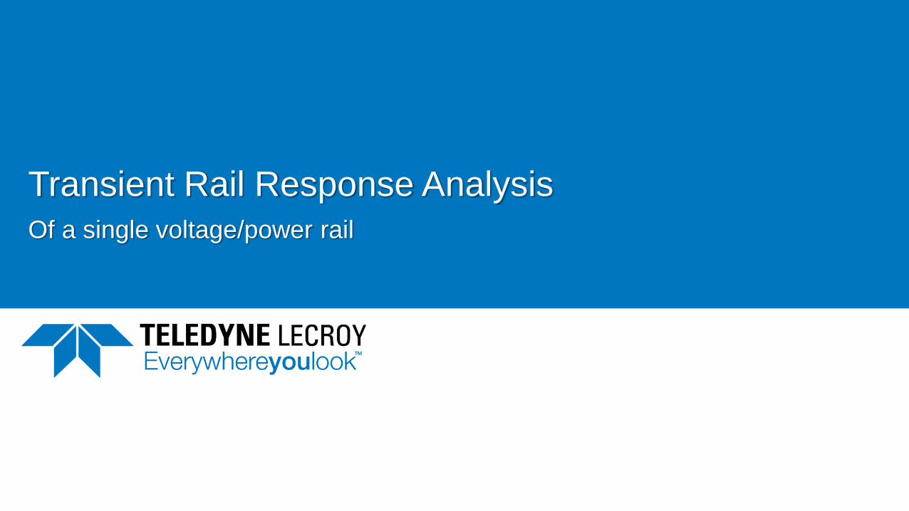
PMIC Transient Rail Response Testing, cont’dFor Multiple Phases in One PMIC
PMIC Load/Current Sharing/Tracking
Measure voltage/current on each
individual phase output
Difficult to do – PMIC normally does not
make output accessible for measuring
current
Phase 1
Phase 4
Phase 3
Phase 2
February 15, 2017 39

Combined Research Project (Oracle + Teledyne LeCroy)
“A Generic Test Tool for Power Distribution Networks”
Dr. Istvan Novak
Senior Principal Engineer, Oracle
Peter Pupalaikis
VP Technology Development, Teledyne LeCroy
Presented February 2, 2017 at DesignCon 2017 in Santa Clara, California (USA)
http://cdn.teledynelecroy.com/files/whitepapers/designcon-2017-a-generic-test-tool-for-power.pdf
February 15, 2017 40

Transient source
3 x AP033
differential
probes
DUT
Lab Setup
HDO81088ch, 12 bit, 1 GHz
oscilloscope
February 15, 2017 41

DUT: 3-phase non-
isolated buck converter
Device Under Test (DUT) Setup
February 15, 2017 42
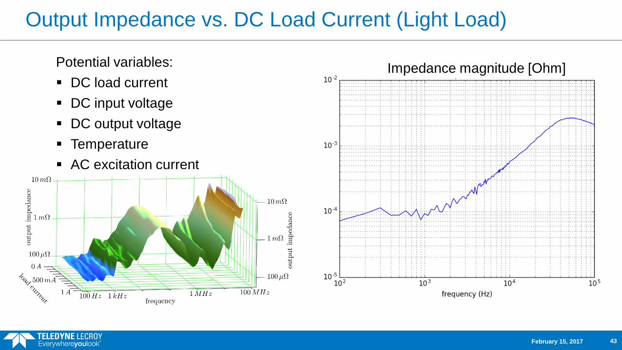
Potential variables:
DC load current
DC input voltage
DC output voltage
Temperature
AC excitation current
Impedance magnitude [Ohm]
Output Impedance vs. DC Load Current (Light Load)
February 15, 2017 43

Output
voltage
transient
Current-
sense
voltage Sum of inductor
currents
Three inductor currents
Transient Current Step
February 15, 2017 44

Current Sharing vs. Frequency
February 15, 2017 45

Voltage/Power Rail Sequence Testing
February 15, 2017 46
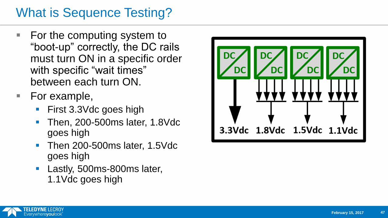
What is Sequence Testing?
For the computing system to “boot-up” correctly, the DC rails must turn ON in a specific order with specific “wait times” between each turn ON.
For example,
First 3.3Vdc goes high
Then, 200-500ms later, 1.8Vdc goes high
Then 200-500ms later, 1.5Vdc goes high
Lastly, 500ms-800ms later, 1.1Vdc goes high
February 15, 2017 47

What are Sequencing Tests?
Acquire as many DC rail signals as possible More is better – great 8ch application
Acquire other signals, e.g.: Clocks
PMIC enable
Strobes
Serial data command signals to PMIC
Measure timing between signals Usually with cursors
Serial TDME options could be useful to some customers
Long capture times with high SR are common 250 Mpts of memory is very useful
Capture a lot of time at high sample rate in many different start-up scenarios, and zoom for details
The image above is a start-up sequencing requirement (timing details are omitted) for a TI embedded ARM microprocessor (http://www.ti.com.cn/product/cn/AM3358-EP/datasheet/6_ZHCSE24A
Note the many different rail voltages (5 different) and multiple 1.8Vdc rails – this is very common Important reason why 8ch is very, very useful
February 15, 2017 48

Voltage/Power Rail Sequence Testing on Power Down50 Mpt capture at 250 MS/s (200 ms) – using timing parameters to measure delta times
February 15, 2017 49
900mV rail
700mV rail
1.5V rail
1.2V rail
1.0V multi-phase rail
Unregulated 1.0V rail
Load current
Measurements of
Delay Time from Ch3
Going Low to Other
Rails Going Low
Scope trigger set to first rail known to go low.
1.0V multi-phase rail
Unregulated 900mV rail
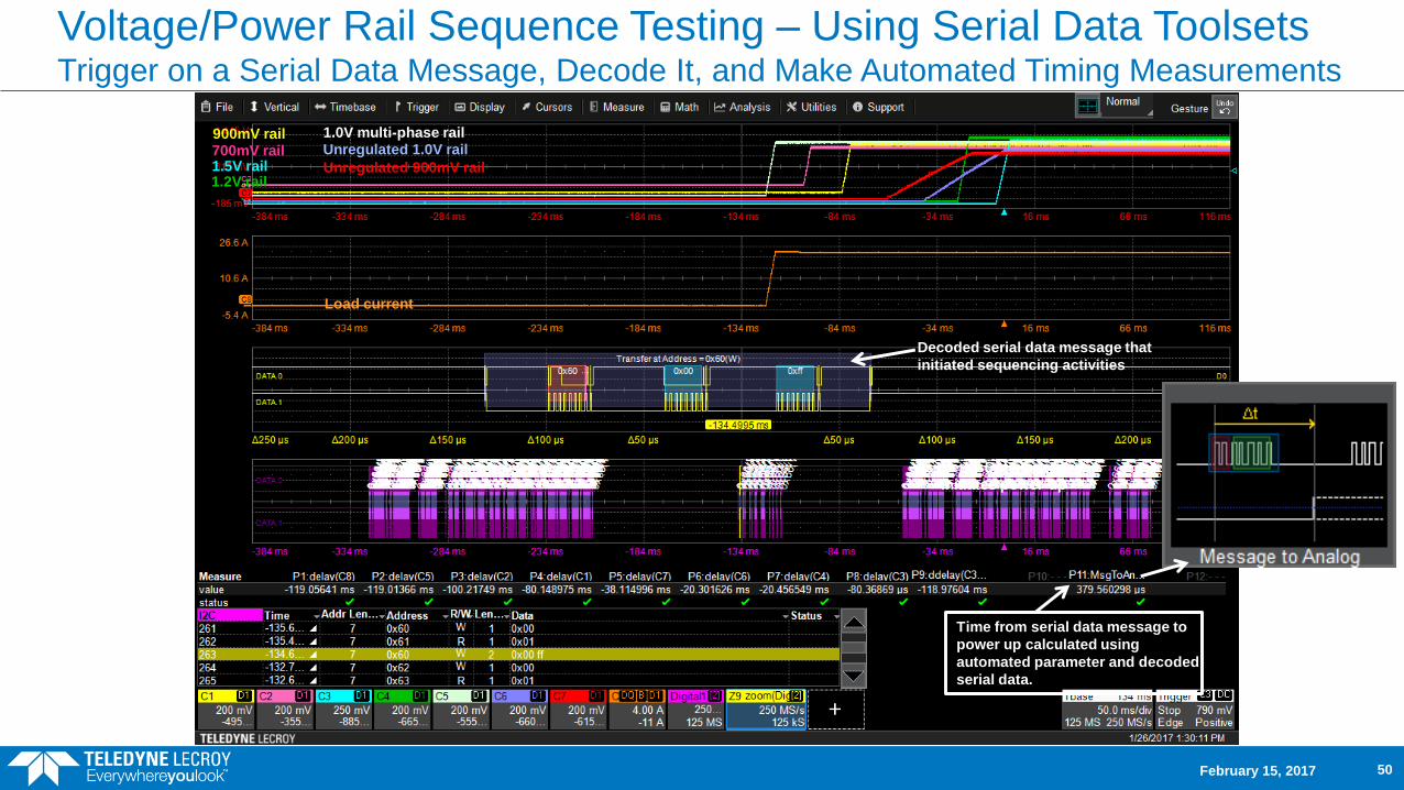
Voltage/Power Rail Sequence Testing – Using Serial Data Toolsets Trigger on a Serial Data Message, Decode It, and Make Automated Timing Measurements
February 15, 2017 50
900mV rail700mV rail1.5V rail1.2V rail
Unregulated 1.0V rail
Load current
Serial Data message
initiates power-up
1.0V multi-phase rail
Unregulated 900mV rail
Time from serial data message to
power up calculated using
automated parameter and decoded
serial data.
Decoded serial data message that
initiated sequencing activities

Serial Data Toolsets – Measurements and Graphing
Timing Measurements
Message to Analog
Analog to Message
Message to Message
Message to Value
“Serial DAC”
Automatic
Run corner cases, gather statistics
Display histograms
Correlate cause-effect timing relationships to other events
February 15, 2017 51

Message to Value parameter
View serial data change over time
Examples
PMbus voltage
I2C or SPI temperature
CAN steering wheel angle
CAN wheel speed (ABS)
I2S audio
“Serial Data DAC” Graphing of Digitally Decoded Data
February 15, 2017 52
Serial Data messages
(100s or 1000s)
Track of Message to Value
parameter
Message to Value
parameter

SPMI (System Power Management Interface) Decoder
SPMI
MIPI standard
More than 20+
other complete
solutions
I2C (PMbus)
UART-RS232
SPI
USB2
HSIC
etc.
February 15, 2017 53

Power Integrity Measurement and Debug Examples
February 15, 2017 54

Power Integrity
Measurement and Debug Example 1
Jitter on a 10 MHz clock circuit is traced back to a
2.9 MHz Point-of-load (POL) DC-DC converter
February 15, 2017 55
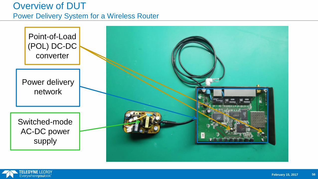
Overview of DUTPower Delivery System for a Wireless Router
Switched-mode
AC-DC power
supply
Point-of-Load
(POL) DC-DC
converter
Power delivery
network
February 15, 2017 56

2.9 MHz POL DC-DC Converter Spectral MeasurementsThe oscilloscope Spectrum Analyzer capability is used to frequency peaks of the POL
February 15, 2017 57
Short Acquisition @ 20 GS/s
Long Acquisition
250 MS/s
Spectrum
Analyzer
Table
Peak Markers
Correspond to Table

POL Ripple Contributes to Clock Jitter JitterKit can be used to quantify jitter on 10 MHz clock and trace it back to the POL
February 15, 2017 58
10 MHz clock acquisition (500 μs long)
TIE Jitter vs. time for the 10 MHz clock
TIE Jitter Overlay of
10 MHz clock
acquisition
TIE Jitter Spectrum of 10
MHz Clock
Histogram of TIE
measurements
Spectrum
Analysis
Table from
2.9 MHz POL

Power Integrity
Measurement and Debug Example 2
Understanding the impact of the power delivery
network (PDN) impedance on clock jitter coupling
February 15, 2017 59

Background - The Importance of Impedance
+
-
+ + + ++
LoadVRM
Bulk Caps Decoupling Caps
Capacitance of Planes
Package
Package Lead Inductance
Control Loop Inductance
+
-LoadVCC
Impedance of PDN
VChip
ZPDN
IMax
Vcc ≠ VChip
February 15, 2017 60

An LDO DC-DC Converter Supplies Power to 10 and 125 MHz Clocks
February 15, 2017 61

Impedance – Measurement Example
+
-LoadVCC
Impedance of PDN
VChip
ZPDN
IMax
February 15, 2017 62
Power Rail Voltage
Measured at VCC
Power Rail Voltage
Measured at VCHIP

10 MHz Clock Causing Ripple on Input Voltage Rail (VCC)
February 15, 2017 63
Long acquisition of VCC
Spectrum Analysis of VCC
Spectrum Analysis
Table of VCC
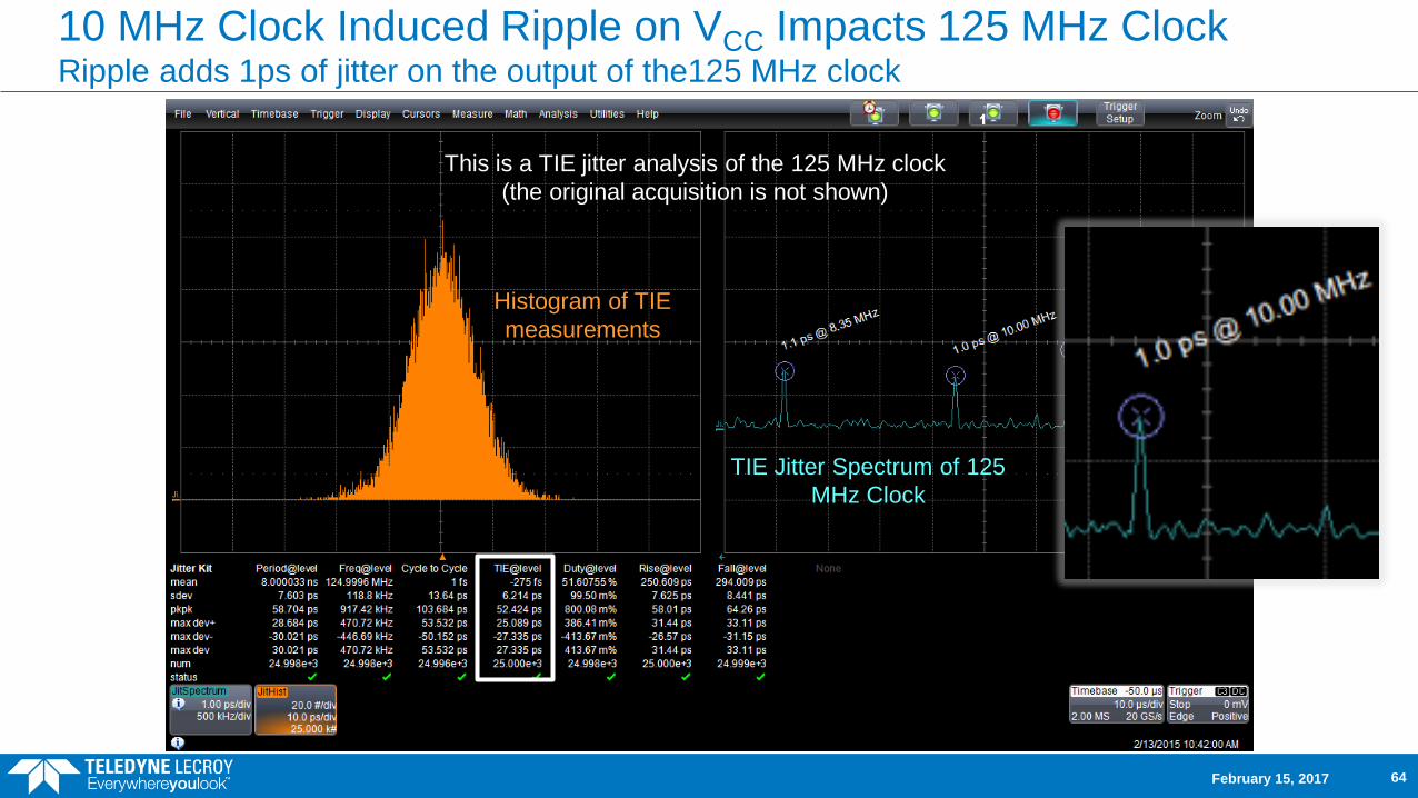
10 MHz Clock Induced Ripple on VCC Impacts 125 MHz ClockRipple adds 1ps of jitter on the output of the125 MHz clock
February 15, 2017 64
TIE Jitter Spectrum of 125
MHz Clock
Histogram of TIE
measurements
This is a TIE jitter analysis of the 125 MHz clock
(the original acquisition is not shown)

Measuring Impedance of the PDNThe plot indicates the impact of the ESR and ESL on the circuit
Omicron Bode 100
40 MHz Network
Analyzer
February 15, 2017 65
Image source http://www.powerelectronictips.com/ceramic-or-
electrolytic-output-capacitors-in-dcdc-converters-why-not-both/
Power/Voltage Rail behaviors during load changes correlate to PDN impedance Equivalent series resistance (ESR) and
inductance (ESL) for half-bridge output capacitor (COut)
Voltage transients at load changes are primarily caused by ESL or impedance of the output cap at very high frequencies.
Slew rates impacted by the reactive power of the capacitor (QC)

A Decoupling Capacitor Can Be Used to Lower ImpedanceTIE jitter is reduced by more than 1psrms in this example
February 15, 2017 66
S301-2 ON w/o
decoupling C
S301-2 ON w/
decoupling C

Power Integrity
Measurement and Debug Example 3
High clock jitter and malfunction can be seen to be
caused by POL DC-DC converter voltage droop.
February 15, 2017 67

POL DC-DC Converter Transient Load ResponseThis provides information about the impedance of the PDN
February 15, 2017 68
Load Current (acquired with a differential voltage probe
and not rescaled to amps)
POL Output Voltage
dI/dt Calculated Waveform
single-phase operation single-phasemulti-phase operation

Transient Load Response Jitter AnalysisThe POL output voltage droop to the clock causes large clock jitter
February 15, 2017 69
TIE Jitter Overlay of 10 MHz clock acquisitionThis persistence overlay of the clock cycles shows very little
jitter with a small number of clock edges having significant jitter
TIE Jitter vs. time for the 10 MHz clockJitter can be seen to vary significantly during voltage droop
200ps TIE Jitter
per vertical
division
POL Output Voltage to 10 MHz clock vs. time100mV droop occurs during step load
Jitter is quantified with
Time Interval Error
measurement. Peak to
peak jitter is 1ns
which is 1/8 of a
period

Transient Load Response – Power Switched on to a Second ClockLoad of second clock causes POL voltage droop and impacts 10 MHz clock functioning
February 15, 2017 70
POL Output Voltage to 10 MHz clock vs. time
Zoom of
above trace
10 MHz Clock Voltage vs. time
Zoom of above trace

Third Polling Question (choose one or more)
What types of testing do you do?
Analysis of a single or multiple voltage/power rail(s)
Multi-phase current tracking/sharing
Power rail sequence testing and timing
Embedded system debug for some/all of the above
None of the above
February 15, 2017 71

Summary
February 15, 2017 72

Teledyne LeCroy Equipment for Digital Power Management, Power Integrity, and Power Sequencing Test and Analysis
February 15, 2017 73
4 or 8 channel, 12 bit, 1 GHz
Oscilloscopes
Comprehensive Probe Offering
DIG-PWR-MGMT
Digital Power Management
Analysis Software Option
Serial Trigger, Decode,
Measure/Graph and Eye Diagram
(TDME) Options
4 channel, 10 bit, 4 GHz
Oscilloscopes
JITKIT
Jitter Kit Toolbox Analysis
Software Option
SPECTRUM
Spectrum Analyzer software
(standard on most HDOs)