Embed Size (px)
Citation preview

This is information on a product in full production.
May 2017 DocID024204 Rev 6 1/33
33
LIS3MDL
Digital output magnetic sensor: ultra-low-power, high-performance 3-axis magnetometer
Datasheet - production data
Features Wide supply voltage, 1.9 V to 3.6 V Independent IO supply (1.8 V) ±4/±8/±12/16 gauss selectable magnetic full
scales Continuous and single-conversion modes 16-bit data output Interrupt generator Self-test I2C/SPI digital output interface Power-down mode / low-power mode ECOPACK®, RoHS and “Green” compliant
Applications Magnetometers Compasses
DescriptionThe LIS3MDL is an ultra-low-power high-performance three-axis magnetic sensor.
The LIS3MDL has user-selectable full scales of ±4/8/12/16 gauss.
The self-test capability allows the user to check the functioning of the sensor in the final application.
The device may be configured to generate interrupt signals for magnetic field detection.
The LIS3MDL includes an I2C serial bus interface that supports standard and fast mode (100 kHz and 400 kHz) and SPI serial standard interface.
The LIS3MDL is available in a small thin plastic land grid array package (LGA) and is guaranteed to operate over an extended temperature range of -40 °C to +85 °C.
LGA-12 (2.0x2.0x1.0 mm)
Table 1. Device summaryOrder codes Temperature range [C] Package Packaging
LIS3MDLTR -40 to +85 LGA-12 Tape and reel
www.st.com

Contents LIS3MDL
2/33 DocID024204 Rev 6
Contents
1 Block diagram and pin description . . . . . . . . . . . . . . . . . . . . . . . . . . . . . 61.1 Block diagram . . . . . . . . . . . . . . . . . . . . . . . . . . . . . . . . . . . . . . . . . . . . . . . 6
1.2 Pin description . . . . . . . . . . . . . . . . . . . . . . . . . . . . . . . . . . . . . . . . . . . . . . 6
2 Magnetic and electrical specifications . . . . . . . . . . . . . . . . . . . . . . . . . . 82.1 Magnetic characteristics . . . . . . . . . . . . . . . . . . . . . . . . . . . . . . . . . . . . . . . 8
2.2 Temperature sensor characteristics . . . . . . . . . . . . . . . . . . . . . . . . . . . . . . 9
2.3 Electrical characteristics . . . . . . . . . . . . . . . . . . . . . . . . . . . . . . . . . . . . . . . 9
2.4 Communication interface characteristics . . . . . . . . . . . . . . . . . . . . . . . . . 102.4.1 SPI - serial peripheral interface . . . . . . . . . . . . . . . . . . . . . . . . . . . . . . . 10
2.4.2 Sensor I2C - inter IC control interface . . . . . . . . . . . . . . . . . . . . . . . . . . 11
2.5 Absolute maximum ratings . . . . . . . . . . . . . . . . . . . . . . . . . . . . . . . . . . . . 12
3 Terminology and functionality . . . . . . . . . . . . . . . . . . . . . . . . . . . . . . . . 133.1 Sensitivity . . . . . . . . . . . . . . . . . . . . . . . . . . . . . . . . . . . . . . . . . . . . . . . . . 13
3.2 Zero-gauss level . . . . . . . . . . . . . . . . . . . . . . . . . . . . . . . . . . . . . . . . . . . . 13
3.3 Factory calibration . . . . . . . . . . . . . . . . . . . . . . . . . . . . . . . . . . . . . . . . . . 13
4 Application hints . . . . . . . . . . . . . . . . . . . . . . . . . . . . . . . . . . . . . . . . . . . 144.1 External capacitors . . . . . . . . . . . . . . . . . . . . . . . . . . . . . . . . . . . . . . . . . . 14
4.2 Soldering information . . . . . . . . . . . . . . . . . . . . . . . . . . . . . . . . . . . . . . . . 14
4.3 High-current wiring effects . . . . . . . . . . . . . . . . . . . . . . . . . . . . . . . . . . . . 15
5 Digital interfaces . . . . . . . . . . . . . . . . . . . . . . . . . . . . . . . . . . . . . . . . . . . 165.1 I2C serial interface . . . . . . . . . . . . . . . . . . . . . . . . . . . . . . . . . . . . . . . . . . 16
5.1.1 I2C operation . . . . . . . . . . . . . . . . . . . . . . . . . . . . . . . . . . . . . . . . . . . . . 17
5.2 SPI bus interface . . . . . . . . . . . . . . . . . . . . . . . . . . . . . . . . . . . . . . . . . . . 185.2.1 SPI read . . . . . . . . . . . . . . . . . . . . . . . . . . . . . . . . . . . . . . . . . . . . . . . . . . . . . . . .20
5.2.2 SPI write . . . . . . . . . . . . . . . . . . . . . . . . . . . . . . . . . . . . . . . . . . . . . . . . . . . . . . .21
5.2.3 SPI read in 3-wire mode . . . . . . . . . . . . . . . . . . . . . . . . . . . . . . . . . . . . . . . . . . .22
6 Register mapping . . . . . . . . . . . . . . . . . . . . . . . . . . . . . . . . . . . . . . . . . . 23

DocID024204 Rev 6 3/33
LIS3MDL Contents
7 Registers description . . . . . . . . . . . . . . . . . . . . . . . . . . . . . . . . . . . . . . . 247.1 WHO_AM_I (0Fh) . . . . . . . . . . . . . . . . . . . . . . . . . . . . . . . . . . . . . . . . . . . 24
7.2 CTRL_REG1 (20h) . . . . . . . . . . . . . . . . . . . . . . . . . . . . . . . . . . . . . . . . . . 24
7.3 CTRL_REG2 (21h) . . . . . . . . . . . . . . . . . . . . . . . . . . . . . . . . . . . . . . . . . . 25
7.4 CTRL_REG3 (22h) . . . . . . . . . . . . . . . . . . . . . . . . . . . . . . . . . . . . . . . . . . 26
7.5 CTRL_REG4 (23h) . . . . . . . . . . . . . . . . . . . . . . . . . . . . . . . . . . . . . . . . . . 26
7.6 CTRL_REG5 (24h) . . . . . . . . . . . . . . . . . . . . . . . . . . . . . . . . . . . . . . . . . . 27
7.7 STATUS_REG (27h) . . . . . . . . . . . . . . . . . . . . . . . . . . . . . . . . . . . . . . . . . 28
7.8 OUT_X_L (28h), OUT_X_H(29h) . . . . . . . . . . . . . . . . . . . . . . . . . . . . . . . 28
7.9 OUT_Y_L (2Ah), OUT_Y_H (2Bh) . . . . . . . . . . . . . . . . . . . . . . . . . . . . . . 28
7.10 OUT_Z_L (2Ch), OUT_Z_H (2Dh) . . . . . . . . . . . . . . . . . . . . . . . . . . . . . . 28
7.11 TEMP_OUT_L (2Eh), TEMP_OUT_H (2Fh) . . . . . . . . . . . . . . . . . . . . . . 28
7.12 INT_CFG (30h) . . . . . . . . . . . . . . . . . . . . . . . . . . . . . . . . . . . . . . . . . . . . . 29
7.13 INT_SRC (31h) . . . . . . . . . . . . . . . . . . . . . . . . . . . . . . . . . . . . . . . . . . . . . 29
7.14 INT_THS_L(32h), INT_THS_H(33h) . . . . . . . . . . . . . . . . . . . . . . . . . . . . 30
8 Package information . . . . . . . . . . . . . . . . . . . . . . . . . . . . . . . . . . . . . . . . 318.1 VFLGA-12 package information . . . . . . . . . . . . . . . . . . . . . . . . . . . . . . . . 31
9 Revision history . . . . . . . . . . . . . . . . . . . . . . . . . . . . . . . . . . . . . . . . . . . 32

List of tables LIS3MDL
4/33 DocID024204 Rev 6
List of tables
Table 1. Device summary . . . . . . . . . . . . . . . . . . . . . . . . . . . . . . . . . . . . . . . . . . . . . . . . . . . . . . . . . . 1Table 2. Pin description . . . . . . . . . . . . . . . . . . . . . . . . . . . . . . . . . . . . . . . . . . . . . . . . . . . . . . . . . . . 7Table 3. Mechanical characteristics . . . . . . . . . . . . . . . . . . . . . . . . . . . . . . . . . . . . . . . . . . . . . . . . . . 8Table 4. Temperature sensor characteristics . . . . . . . . . . . . . . . . . . . . . . . . . . . . . . . . . . . . . . . . . . . 9Table 5. Electrical characteristics . . . . . . . . . . . . . . . . . . . . . . . . . . . . . . . . . . . . . . . . . . . . . . . . . . . . 9Table 6. SPI slave timing values. . . . . . . . . . . . . . . . . . . . . . . . . . . . . . . . . . . . . . . . . . . . . . . . . . . . 10Table 7. I2C slave timing values . . . . . . . . . . . . . . . . . . . . . . . . . . . . . . . . . . . . . . . . . . . . . . . . . . . . 11Table 8. Absolute maximum ratings . . . . . . . . . . . . . . . . . . . . . . . . . . . . . . . . . . . . . . . . . . . . . . . . . 12Table 9. Serial interface pin description . . . . . . . . . . . . . . . . . . . . . . . . . . . . . . . . . . . . . . . . . . . . . . 16Table 10. I2C terminology . . . . . . . . . . . . . . . . . . . . . . . . . . . . . . . . . . . . . . . . . . . . . . . . . . . . . . . . . . 16Table 11. SAD+read/write patterns. . . . . . . . . . . . . . . . . . . . . . . . . . . . . . . . . . . . . . . . . . . . . . . . . . . 17Table 12. Transfer when master is writing one byte to slave . . . . . . . . . . . . . . . . . . . . . . . . . . . . . . . 17Table 13. Transfer when master is writing multiple bytes to slave . . . . . . . . . . . . . . . . . . . . . . . . . . . 18Table 14. Transfer when master is receiving (reading) one byte of data from slave . . . . . . . . . . . . . 18Table 15. Transfer when master is receiving (reading) multiple bytes of data from slave . . . . . . . . . 18Table 16. Register address map. . . . . . . . . . . . . . . . . . . . . . . . . . . . . . . . . . . . . . . . . . . . . . . . . . . . . 23Table 17. WHO_AM_I register . . . . . . . . . . . . . . . . . . . . . . . . . . . . . . . . . . . . . . . . . . . . . . . . . . . . . . 24Table 18. CTRL_REG1 register . . . . . . . . . . . . . . . . . . . . . . . . . . . . . . . . . . . . . . . . . . . . . . . . . . . . . 24Table 19. CTRL_REG1 description . . . . . . . . . . . . . . . . . . . . . . . . . . . . . . . . . . . . . . . . . . . . . . . . . . 24Table 20. Data rate configuration . . . . . . . . . . . . . . . . . . . . . . . . . . . . . . . . . . . . . . . . . . . . . . . . . . . . 24Table 21. X and Y axes operating mode selection . . . . . . . . . . . . . . . . . . . . . . . . . . . . . . . . . . . . . . . 25Table 22. Output data rate configuration . . . . . . . . . . . . . . . . . . . . . . . . . . . . . . . . . . . . . . . . . . . . . . 25Table 23. CTRL_REG2 register . . . . . . . . . . . . . . . . . . . . . . . . . . . . . . . . . . . . . . . . . . . . . . . . . . . . . 25Table 24. CTRL_REG2 description . . . . . . . . . . . . . . . . . . . . . . . . . . . . . . . . . . . . . . . . . . . . . . . . . . 25Table 25. Full-scale selection . . . . . . . . . . . . . . . . . . . . . . . . . . . . . . . . . . . . . . . . . . . . . . . . . . . . . . . 25Table 26. CTRL_REG3 register . . . . . . . . . . . . . . . . . . . . . . . . . . . . . . . . . . . . . . . . . . . . . . . . . . . . . 26Table 27. CTRL_REG3 description . . . . . . . . . . . . . . . . . . . . . . . . . . . . . . . . . . . . . . . . . . . . . . . . . . 26Table 28. System operating mode selection. . . . . . . . . . . . . . . . . . . . . . . . . . . . . . . . . . . . . . . . . . . . 26Table 29. CTRL_REG4 register . . . . . . . . . . . . . . . . . . . . . . . . . . . . . . . . . . . . . . . . . . . . . . . . . . . . . 26Table 30. CTRL_REG4 description . . . . . . . . . . . . . . . . . . . . . . . . . . . . . . . . . . . . . . . . . . . . . . . . . . 26Table 31. Z-axis operating mode selection. . . . . . . . . . . . . . . . . . . . . . . . . . . . . . . . . . . . . . . . . . . . . 27Table 32. CTRL_REG5 register . . . . . . . . . . . . . . . . . . . . . . . . . . . . . . . . . . . . . . . . . . . . . . . . . . . . . 27Table 33. CTRL_REG5 description . . . . . . . . . . . . . . . . . . . . . . . . . . . . . . . . . . . . . . . . . . . . . . . . . . 27Table 34. STATUS_REG register . . . . . . . . . . . . . . . . . . . . . . . . . . . . . . . . . . . . . . . . . . . . . . . . . . . . 28Table 35. STATUS_REG description . . . . . . . . . . . . . . . . . . . . . . . . . . . . . . . . . . . . . . . . . . . . . . . . . 28Table 36. INT_CFG register . . . . . . . . . . . . . . . . . . . . . . . . . . . . . . . . . . . . . . . . . . . . . . . . . . . . . . . . 29Table 37. INT_CFG description . . . . . . . . . . . . . . . . . . . . . . . . . . . . . . . . . . . . . . . . . . . . . . . . . . . . . 29Table 38. INT_SRC register . . . . . . . . . . . . . . . . . . . . . . . . . . . . . . . . . . . . . . . . . . . . . . . . . . . . . . . . 29Table 39. INT_SRC description . . . . . . . . . . . . . . . . . . . . . . . . . . . . . . . . . . . . . . . . . . . . . . . . . . . . . 29Table 40. INT_THS_L_M . . . . . . . . . . . . . . . . . . . . . . . . . . . . . . . . . . . . . . . . . . . . . . . . . . . . . . . . . . 30Table 41. INT_THS_H_M . . . . . . . . . . . . . . . . . . . . . . . . . . . . . . . . . . . . . . . . . . . . . . . . . . . . . . . . . . 30Table 42. VFLGA 2x2x1 12LD pitch 0.5 mm package mechanical data. . . . . . . . . . . . . . . . . . . . . . . 31Table 43. Document revision history. . . . . . . . . . . . . . . . . . . . . . . . . . . . . . . . . . . . . . . . . . . . . . . . . . 32

DocID024204 Rev 6 5/33
LIS3MDL List of figures
List of figures
Figure 1. Block diagram . . . . . . . . . . . . . . . . . . . . . . . . . . . . . . . . . . . . . . . . . . . . . . . . . . . . . . . . . . . . 6Figure 2. Pin connections . . . . . . . . . . . . . . . . . . . . . . . . . . . . . . . . . . . . . . . . . . . . . . . . . . . . . . . . . . 6Figure 3. SPI slave timing diagram . . . . . . . . . . . . . . . . . . . . . . . . . . . . . . . . . . . . . . . . . . . . . . . . . . . . . . . . . . . . . . . . . . . . . . . . .10
Figure 4. I2C slave timing diagram . . . . . . . . . . . . . . . . . . . . . . . . . . . . . . . . . . . . . . . . . . . . . . . . . . 11Figure 5. LIS3MDL electrical connections . . . . . . . . . . . . . . . . . . . . . . . . . . . . . . . . . . . . . . . . . . . . . 14Figure 6. Read and write protocol . . . . . . . . . . . . . . . . . . . . . . . . . . . . . . . . . . . . . . . . . . . . . . . . . . . 19Figure 7. SPI read protocol . . . . . . . . . . . . . . . . . . . . . . . . . . . . . . . . . . . . . . . . . . . . . . . . . . . . . . . . 20Figure 8. Multiple byte SPI read protocol (2-byte example) . . . . . . . . . . . . . . . . . . . . . . . . . . . . . . . . 20Figure 9. SPI write protocol . . . . . . . . . . . . . . . . . . . . . . . . . . . . . . . . . . . . . . . . . . . . . . . . . . . . . . . . 21Figure 10. Multiple byte SPI write protocol (2-byte example). . . . . . . . . . . . . . . . . . . . . . . . . . . . . . . . 21Figure 11. SPI read protocol in 3-wire mode . . . . . . . . . . . . . . . . . . . . . . . . . . . . . . . . . . . . . . . . . . . . 22Figure 12. VFLGA 2x2x1 12LD pitch 0.5 mm package outline . . . . . . . . . . . . . . . . . . . . . . . . . . . . . . 31

Block diagram and pin description LIS3MDL
6/33 DocID024204 Rev 6
1 Block diagram and pin description
1.1 Block diagram
Figure 1. Block diagram
1.2 Pin description
Figure 2. Pin connections
I (M)
Y+
Z+
Y-
Z-
X+
X-
CHARGEAMPLIFIER
I2C
SPI
CS
SCL/SPC
SDA/SDI/SDO
SDO/SA1
CONTROL LOGICCLOCKTRIMMINGCIRCUITS
A/D CONTROL
CONVERTERMUX LOGIC
INTERRUPTGENERATOR
Vdd_
IO
C1
SCL/SPC
Res
GNDDRDY
Vdd
Res
CS
BOTTOM VIEW
4
1
56INT
11 12
SDA/
SDI/S
DO
7
10
SD0/SA1
TOP VIEW
DIRECTION OFDETECTABLEMAGNETIC FIELDS
X
Z
Y

DocID024204 Rev 6 7/33
LIS3MDL Block diagram and pin description
Table 2. Pin description Pin# Name Function
1SCLSPC
I2C serial clock (SCL)SPI serial port clock (SPC)
2 Reserved Connect to GND
3 GND Connect to GND
4 C1 Capacitor connection (C1=100 nF)
5 Vdd Power supply
6 Vdd_IO Power supply for I/O pins
7 INT Interrupt
8 DRDY Data Ready
9SDOSA1
SPI serial data output (SDO)I2C less significant bit of the device address (SA1)
10 CS
SPI enableI2C/SPI mode selection (1: SPI idle mode / I2C communication enabled; 0: SPI communication mode / I2C disabled)
11SDASDISDO
I2C serial data (SDA)SPI serial data input (SDI)3-wire interface serial data output (SDO)
12 Reserved Connect to GND

Magnetic and electrical specifications LIS3MDL
8/33 DocID024204 Rev 6
2 Magnetic and electrical specifications
2.1 Magnetic characteristics@ Vdd = 2.5 V, T = 25 °C unless otherwise noted(a)
a. The product is factory calibrated at 2.5 V. The operational power supply range is from 1.9 V to 3.6 V.
Table 3. Mechanical characteristics Symbol Parameter Test conditions Min. Typ.(1) Max. Unit
FS Measurement range
±4
gauss±8
±12
±16
GN Sensitivity
FS=±4 gauss 6842
LSB/gauss
FS=±8 gauss 3421
FS=±12 gauss 2281
FS=±16 gauss 1711
Zgauss Zero-gauss level FS=±4 gauss ±1 gauss
RMS RMS noise
X-axis; FS=±12 gauss; Ultra-high-performance mode
3.2 mgauss
Y-axis; FS=±12 gaussUltra-high-performance mode
3.2 mgauss
Z-axis; FS=±12 gaussUltra-high-performance mode
4.1 mgauss
NL Non-linearityBest-fit straight lineFS = ±12 gaussHapplied = ±6 gauss
±0.12 %FS
ST Self test(2)
X-axisFS = ±12 gauss
1 3
gaussY-axisFS = ±12 gauss
1 3
Z-axisFS = ±12 gauss
0.1 1
DF Magnetic disturbance field Zero-gauss offset starts to degrade 50 gauss
Top Operating temperature range -40 +85 °C
1. Typical specifications are not guaranteed.
2. Absolute value.

DocID024204 Rev 6 9/33
LIS3MDL Magnetic and electrical specifications
2.2 Temperature sensor characteristics@ Vdd = 2.5 V, T = 25 °C unless otherwise noted(b).
2.3 Electrical characteristics@ Vdd = 2.5 V, T = 25 °C unless otherwise noted(c)
b. The product is factory calibrated at 2.5 V.
Table 4. Temperature sensor characteristicsSymbol Parameter Test conditions Min. Typ.(1) Max. Unit
TSDr Temperature sensor output change vs. temperature - 8 LSB/°C
TODR Temperature refresh rate(2) ODR Hz
Top Operating temperature range -40 +85 °C
1. Typical specifications are not guaranteed.
2. If TEMP_EN bit in CTRL_REG1 (20h) is set to’1’, a temperature data is acquired at each conversion cycle. Refer to Table 22.
c. The product is factory calibrated at 2.5 V. The operational power supply range is from 1.9 V to 3.6 V.
Table 5. Electrical characteristicsSymbol Parameter Test conditions Min. Typ.(1) Max. Unit
Vdd Supply voltage 1.9 3.6 V
Vdd_IO Power supply for I/O 1.71 1.8 Vdd+0.1
Idd_HRCurrent consumption in ultra-high-resolution mode
ODR = 20 Hz 270 μA
Idd_LPCurrent consumption inlow-power mode
ODR = 20 Hz 40 μA
Idd_PDCurrent consumption in power down
1 μA
Top Operating temperature range -40 +85 °C
1. Typical specification are not guaranteed.

Magnetic and electrical specifications LIS3MDL
10/33 DocID024204 Rev 6
2.4 Communication interface characteristics
2.4.1 SPI - serial peripheral interfaceSubject to general operating conditions for Vdd and Top.
Figure 3. SPI slave timing diagram
Note: Measurement points are done at 0.2• Vdd_IO and 0.8• Vdd_IO, for both input and output ports.
Table 6. SPI slave timing values
Symbol ParameterValue (1)
1. Values are guaranteed at 10 MHz clock frequency for SPI with both 4 and 3 wires, based on characterization results, not tested in production.
UnitMin. Max.
tc(SPC) SPI clock cycle 100 ns
fc(SPC) SPI clock frequency 10 MHz
tsu(CS) CS setup time 5
ns
th(CS) CS hold time 20
tsu(SI) SDI input setup time 5
th(SI) SDI input hold time 15
tv(SO) SDO valid output time 50
th(SO) SDO output hold time 5
tdis(SO) SDO output disable time 50
SPC
CS
SDI
SDO
tsu(CS)
tv(SO) th(SO)
th(SI)tsu(SI)
th(CS)
tdis(SO)
tc(SPC)
MSB IN
MSB OUT LSB OUT
LSB IN

DocID024204 Rev 6 11/33
LIS3MDL Magnetic and electrical specifications
2.4.2 Sensor I2C - inter IC control interfaceSubject to general operating conditions for Vdd and Top.
Figure 4. I2C slave timing diagram
Note: Measurement points are done at 0.2• Vdd_IO and 0.8• Vdd_IO, for both ports.
Table 7. I2C slave timing values
Symbol ParameterI2C standard mode (1) I2C fast mode (1)
UnitMin. Max. Min. Max.
f(SCL) SCL clock frequency 0 100 0 400 kHz
tw(SCLL) SCL clock low time 4.7 1.3μs
tw(SCLH) SCL clock high time 4.0 0.6
tsu(SDA) SDA setup time 250 100 ns
th(SDA) SDA data hold time 0 3.45 0 0.9 μs
tr(SDA) tr(SCL) SDA and SCL rise time 1000 20 + 0.1Cb(2) 300
nstf(SDA) tf(SCL) SDA and SCL fall time 300 20 + 0.1Cb
(2) 300
th(ST) START condition hold time 4 0.6
μstsu(SR)
Repeated START condition setup time 4.7 0.6
tsu(SP) STOP condition setup time 4 0.6
tw(SP:SR)Bus free time between STOP and START condition 4.7 1.3
1. Data based on standard I2C protocol requirement, not tested in production.
2. Cb = total capacitance of one bus line, in pF.

Magnetic and electrical specifications LIS3MDL
12/33 DocID024204 Rev 6
2.5 Absolute maximum ratingsStresses above those listed as “absolute maximum ratings” may cause permanent damage to the device. This is a stress rating only and functional operation of the device under these conditions is not implied. Exposure to maximum rating conditions for extended periods may affect device reliability.
Note: Supply voltage on any pin should never exceed 4.8 V.
Table 8. Absolute maximum ratingsSymbol Ratings Maximum value Unit
Vdd Supply voltage -0.3 to 4.8 V
Vdd_IO I/O pins supply voltage -0.3 to 4.8 V
Vin Input voltage on any control pin (SCL/SPC, SDA/SDI/SDO, SDO/SA1, CS) -0.3 to Vdd_IO +0.3 V
AUNP Acceleration (any axis)3,000 for 0.5 ms g
10,000 for 0.1 ms g
MEF Maximum exposed field 1000 gauss
TOP Operating temperature range -40 to +85 °C
TSTG Storage temperature range -40 to +125 °C
This device is sensitive to magnetic fields, improper handling can cause permanent damage to the part.
This device is sensitive to electrostatic discharge (ESD), improper handling can cause permanent damage to the part.

DocID024204 Rev 6 13/33
LIS3MDL Terminology and functionality
3 Terminology and functionality
3.1 SensitivitySensitivity describes the gain of the sensor and can be determined, for example, by applying a magnetic field of 1 gauss to it.
3.2 Zero-gauss levelZero-gauss level offset describes the deviation of an actual output signal from the ideal output if no magnetic field is present.
3.3 Factory calibrationThe IC interface is factory calibrated for sensitivity (So) and Zero-gauss level (TyOff).
The trimming values are stored in the device in non-volatile memory. Each time the device is turned on, the trimming parameters are downloaded to the registers to be employed during active operation which allows using the device without further calibration.

Application hints LIS3MDL
14/33 DocID024204 Rev 6
4 Application hints
Figure 5. LIS3MDL electrical connections
4.1 External capacitorsThe LIS3MDL requires one external capacitor (C1 = 100 nF) connected between pin 4 and GND.
The device core power supply line (Vdd) needs one high-frequency decoupling capacitor (C3 = 100 nF, ceramic) as near as possible to the supply pin, and a low-frequency electrolytic capacitor (C2 = 1 μF). All the voltage and ground supplies must be present at the same time to have proper behavior of the IC (refer to Figure 5).
The functionality of the device and the measured magnetic field data is selectable and accessible through the I2C / SPI interfaces.
The functions, the threshold and the timing of the interrupt pin (INT) can be completely programmed by the user through the I2C / SPI interfaces.
When I2C or 3-wire SPI is used, the SDO/SA1 pin must be connected to Vdd_IO or GND.
4.2 Soldering informationThe LGA package is compliant with the ECOPACK®, RoHS and “Green” standard.It is qualified for soldering heat resistance according to JEDEC J-STD-020.
Land pattern and soldering recommendations are available at www.st.com.
Vdd
C 3 =100 nF
GND
SDA
/SD
I/SD
O
SCL/
SPC
C 2 =1 µF
4
1
55 77
1112
Vdd_IO
CS
C 1 =100 nF
(TOP VIEW)
10
SDO/SA1
DRDY8
INT6
92
3
TOP VIEW
DIRECTION OFDETECTABLEMAGNETIC FIELDS
X
Z
Y

DocID024204 Rev 6 15/33
LIS3MDL Application hints
4.3 High-current wiring effectsHigh current in wiring and printed circuit traces can cause errors in magnetic field measurements for compassing.
Conductor-generated magnetic fields will add to the Earth’s magnetic field, causing errors in compass heading computation.
Keep currents higher than 10 mA a few millimeters away from the sensor IC.

Digital interfaces LIS3MDL
16/33 DocID024204 Rev 6
5 Digital interfaces
The registers embedded in the LIS3MDL may be accessed through both the I2C and SPI serial interfaces. The latter may be SW configured to operate either in 3-wire or 4-wire interface mode.
The serial interfaces are mapped to the same pads. To select/exploit the I2C interface, the CS line must be tied high (i.e. connected to Vdd_IO).
5.1 I2C serial interfaceThe LIS3MDL I2C is a bus slave. The I2C is employed to write data to registers whose content can also be read back.
The relevant I2C terminology is given in the table below.
There are two signals associated with the I2C bus: the serial clock line (SCL) and the serial data line (SDA). The latter is a bidirectional line used for sending and receiving the data to/from the interface. Both lines must be connected to Vdd_IO through an external pull-up resistor. When the bus is free, both the lines are high.
The I2C interface is compliant with fast mode (400 kHz) I2C standards, as well as with normal mode.
When the I2C interface is used, the SDO/SA1 pin has to be connected to Vdd_IO or GND.
Table 9. Serial interface pin descriptionPin name Pin description
CSSPI enableI2C/SPI mode selection (1: SPI idle mode / I2C communication enabled; 0: SPI communication mode / I2C disabled)
SCLSPC
I2C serial clock (SCL)SPI serial port clock (SPC)
SDASDISDO
I2C serial data (SDA)SPI serial data input (SDI)3-wire interface serial data output (SDO)
SA1SDO
I2C less significant bit of the device address (SA1)SPI serial data output (SDO)
Table 10. I2C terminologyTerm Description
Transmitter The device which sends data to the bus
Receiver The device which receives data from the bus
Master The device which initiates a transfer, generates clock signals and terminates a transfer
Slave The device addressed by the master

DocID024204 Rev 6 17/33
LIS3MDL Digital interfaces
5.1.1 I2C operationThe transaction on the bus is started through a START (ST) signal. A START condition is defined as a HIGH-to-LOW transition on the data line while the SCL line is held HIGH. After this has been transmitted by the master, the bus is considered busy. The next byte of data transmitted after the start condition contains the address of the slave in the first seven bits and the eighth bit tells whether the master is receiving data from the slave or transmitting data to the slave. When an address is sent, each device in the system compares the first seven bits after a start condition with its address. If they match, the device considers itself addressed by the master.
The Slave ADdress (SAD) associated to the LIS3MDL is 00111x0b, whereas the x bit is modified by the SDO/SA1 pin in order to modify the device address. If the SDO/SA1 pin is connected to the voltage supply, the address is 0011110b, otherwise, if the SDO/SA1 pin is connected to ground, the address is 0011100b.
Data transfer with acknowledge is mandatory. The transmitter must release the SDA line during the acknowledge pulse. The receiver must then pull the data line LOW so that it remains stable low during the HIGH period of the acknowledge clock pulse. A receiver which has been addressed is obliged to generate an acknowledge after each byte of data received.
The I2C embedded inside the LIS3MDL behaves like a slave device and the following protocol must be adhered to. After the START condition (ST) a slave address is sent, once a slave acknowledge (SAK) has been returned, an 8-bit sub-address (SUB) is transmitted: the 7 LSb represent the actual register address while the MSb enables address auto-increment. If the MSb of the SUB field is ‘1’, the SUB (register address) is automatically increased to allow multiple data read/write.
The slave address is completed with a Read/Write bit. If the bit is ‘1’ (Read), a repeated START (SR) condition must be issued after the two sub-address bytes; if the bit is ‘0’ (Write) the master will transmit to the slave with direction unchanged. Table 11 explains how the SAD+read/write bit pattern is composed, listing all the possible configurations.
Table 11.SAD+read/write patternsCommand SAD[6:2] SAD[1] = SDO/SA1 SAD[0] R/W SAD+R/W
Read 00111 0 0 1 00111001 (39h)
Write 00111 0 0 0 00111000 (38h)
Read 00111 1 0 1 00111101 (3Dh)
Write 00111 1 0 0 00111100 (3Ch)
Table 12. Transfer when master is writing one byte to slaveMaster ST SAD + W SUB DATA SP
Slave SAK SAK SAK

Digital interfaces LIS3MDL
18/33 DocID024204 Rev 6
Data are transmitted in byte format (DATA). Each data transfer contains 8 bits. The number of bytes transferred per transfer is unlimited. Data is transferred with the most significant bit (MSb) first. If a receiver cannot receive another complete byte of data until it has performed some other function, it can hold the clock line SCL LOW to force the transmitter into a wait state. Data transfer only continues when the receiver is ready for another byte and releases the data line. If a slave receiver does not acknowledge the slave address (i.e. it is not able to receive because it is performing some real-time function) the data line must be left HIGH by the slave. The Master can then abort the transfer. A LOW to HIGH transition on the SDA line while the SCL line is HIGH is defined as a STOP condition. Each data transfer must be terminated by the generation of a STOP (SP) condition.
In order to read multiple bytes, it is necessary to assert the most significant bit of the sub-address field. In other words, SUB(7) must be equal to 1, while SUB(6-0) represents the address of first register to be read.
In the presented communication format, MAK is Master acknowledge and NMAK is No Master Acknowledge.
5.2 SPI bus interfaceThe LIS3MDL SPI is a bus slave. The SPI allows writing to and reading from the registers of the device.
The serial interface interacts with the application through 4 wires: CS, SPC, SDI and SDO.
Table 13. Transfer when master is writing multiple bytes to slaveMaster ST SAD + W SUB DATA DATA SP
Slave SAK SAK SAK SAK
Table 14. Transfer when master is receiving (reading) one byte of data from slaveMaster ST SAD + W SUB SR SAD + R NMAK SP
Slave SAK SAK SAK DATA
Table 15. Transfer when master is receiving (reading) multiple bytes of data from slaveMaster ST SAD+W SUB SR SAD+R MAK MAK NMAK SP
Slave SAK SAK SAK DATA DATA DATA

DocID024204 Rev 6 19/33
LIS3MDL Digital interfaces
Figure 6. Read and write protocol
CS is the serial port enable and it is controlled by the SPI master. It goes low at the start of the transmission and goes back high at the end. SPC is the serial port clock and it is controlled by the SPI master. It is stopped high when CS is high (no transmission). SDI and SDO are respectively the serial port data input and output. Those lines are driven at the falling edge of SPC and should be captured at the rising edge of SPC.
Both the read register and write register commands are completed in 16 clock pulses or in multiples of 8 in case of multiple byte read/write. Bit duration is the time between two falling edges of SPC. The first bit (bit 0) starts at the first falling edge of SPC after the falling edge of CS while the last bit (bit 15, bit 23, ...) starts at the last falling edge of SPC just before the rising edge of CS.
bit 0: RW bit. When 0, the data DI(7:0) is written into the device. When 1, the data DO(7:0) from the device is read. In latter case, the chip will drive SDO at the start of bit 8.
bit 1: MS bit. When 0, the address will remain unchanged in multiple read/write commands. When 1, the address is auto-incremented in multiple read/write commands.
bit 2-7: address AD(5:0). This is the address field of the indexed register.
bit 8-15: data DI(7:0) (write mode). This is the data that is written into the device (MSb first).
bit 8-15: data DO(7:0) (read mode). This is the data that is read from the device (MSb first).
In multiple read/write commands further blocks of 8 clock periods will be added. When the MS bit is ‘0’, the address used to read/write data remains the same for every block. When the MS bit is ‘1’, the address used to read/write data is increased at every block.
The function and the behavior of SDI and SDO remain unchanged.
CS
SPC
SDI
SDO
RWAD5 AD4 AD3 AD2 AD1 AD0
DI7 DI6 DI5 DI4 DI3 DI2 DI1 DI0
DO7 DO6 DO5 DO4 DO3 DO2 DO1 DO0
MS
AM10129V1

Digital interfaces LIS3MDL
20/33 DocID024204 Rev 6
5.2.1 SPI read
Figure 7. SPI read protocol
The SPI read command is performed with 16 clock pulses. A multiple byte read command is performed by adding blocks of 8 clock pulses to the previous one.
bit 0: READ bit. The value is 1.
bit 1: MS bit. When 0, does not increment address; when 1, increments the address in multiple reads.
bit 2-7: address AD(5:0). This is the address field of the indexed register.
bit 8-15: data DO(7:0) (read mode). This is the data that will be read from the device (MSb first).
bit 16-... : data DO(...-8). Further data in multiple byte reads.
Figure 8. Multiple byte SPI read protocol (2-byte example)
CS
SPC
SDI
SDO
RW
DO7 DO6 DO5 DO4 DO3 DO2 DO1 DO0
AD5 AD4 AD3 AD2 AD1 AD0MS
AM10130V1
C S
SPC
SDI
SD O
RW
DO 7 DO 6 DO 5 DO 4 DO 3 DO 2 DO 1 DO 0
AD5 AD4 AD 3 AD2 AD1 AD0
DO 15 DO 14 DO 13 DO 12 DO 11 DO 10 D O9 D O8
M S
AM10131V1

DocID024204 Rev 6 21/33
LIS3MDL Digital interfaces
5.2.2 SPI write
Figure 9. SPI write protocol
The SPI Write command is performed with 16 clock pulses. A multiple byte write command is performed by adding blocks of 8 clock pulses to the previous one.
bit 0: WRITE bit. The value is 0.
bit 1: MS bit. When 0, does not increment the address; when 1, increments the address in multiple writes.
bit 2 -7: address AD(5:0). This is the address field of the indexed register.
bit 8-15: data DI(7:0) (write mode). This is the data that is written inside the device (MSb first).
bit 16-... : data DI(...-8). Further data in multiple byte writes.
Figure 10. Multiple byte SPI write protocol (2-byte example)
CS
SPC
SDIRW DI7 DI6 DI5 DI4 DI3 DI2 DI1 DI0
AD5 AD4 AD3 AD2 AD1 AD0MS
AM10132V1
CS
SPC
SDI
RW
AD5 AD4 AD3 AD2 AD1 AD0
DI7 DI6 DI5 DI4 DI3 DI2 DI1 DI0 DI15 DI14 DI13 DI12 DI11 DI10 DI9 DI8
MS
AM10133V1

Digital interfaces LIS3MDL
22/33 DocID024204 Rev 6
5.2.3 SPI read in 3-wire mode3-wire mode is entered by setting bit SIM to ‘1’ (SPI serial interface mode selection) in CTRL_REG3 (22h).
When 3-wire mode is used, the SDO/SA1 pin has to be connected to GND or Vdd_IO.
Figure 11. SPI read protocol in 3-wire mode
The SPI read command is performed with 16 clock pulses:
bit 0: READ bit. The value is 1.
bit 1: MS bit. When 0, does not increment the address; when 1, increments the address in multiple reads.
bit 2-7: address AD(5:0). This is the address field of the indexed register.
bit 8-15: data DO(7:0) (read mode). This is the data that is read from the device (MSb first).
A multiple read command is also available in 3-wire mode.
CS
SPC
SDI/O
RW DO7 DO6 DO5 DO4 DO3 DO2 DO1 DO0
AD5 AD4 AD3 AD2 AD1 AD0MS
AM10134V1

DocID024204 Rev 6 23/33
LIS3MDL Register mapping
6 Register mapping
The table below provides a list of the 8-bit registers embedded in the device and their respective addresses.
Registers marked Reserved or not listed in the table above must not be changed. Writing to those registers may cause permanent damage to the device.
The content of the registers that are loaded at boot should not be changed. They contain the factory calibration values. Their content is automatically restored when the device is powered up.
Table 16. Register address map
Name TypeRegister address
Default CommentHex Binary
Reserved 00 - 0E -- -- Reserved
WHO_AM_I r 0F 0000 1111 00111101 Dummy register
Reserved 10 - 1F -- -- Reserved
CTRL_REG1 r/w 20 0010 0000 00010000
CTRL_REG2 r/w 21 0010 0001 00000000
CTRL_REG3 r/w 22 0010 0010 00000011
CTRL_REG4 r/w 23 0010 0011 00000000
CTRL_REG5 r/w 24 0010 0100 00000000
Reserved 25 - 26 -- -- Reserved
STATUS_REG r 27 0010 0111 Output
OUT_X_L r 28 0010 1000 Output
OUT_X_H r 29 0010 1001 Output
OUT_Y_L r 2A 0010 1010 Output
OUT_Y_H r 2B 0010 1011 Output
OUT_Z_L r 2C 0010 1100 Output
OUT_Z_H r 2D 0010 1101 Output
TEMP_OUT_L r 2E 0010 1110 Output
TEMP_OUT_H r 2F 0010 1111 Output
INT_CFG r/w 30 00110000 11101000
INT_SRC r 31 00110001 00000000
INT_THS_L r/w 32 00110010 00000000
INT_THS_H r/w 33 00110011 00000000

Registers description LIS3MDL
24/33 DocID024204 Rev 6
7 Registers description
7.1 WHO_AM_I (0Fh)
Device identification register.
7.2 CTRL_REG1 (20h)
Table 17. WHO_AM_I register0 0 1 1 1 1 0 1
Table 18. CTRL_REG1 registerTEMP_EN OM1 OM0 DO2 DO1 DO0 FAST_ODR ST
Table 19. CTRL_REG1 description
TEMP_ENTemperature sensor enable. Default value: 0(0: temperature sensor disabled; 1: temperature sensor enabled)
OM[1:0]X and Y axes operative mode selection. Default value: 00(Refer to Table 21)
DO[2:0]Output data rate selection. Default value: 100(Refer to Table 22)
FAST_ODRFAST_ODR enables data rates higher than 80 Hz (refer to Table 20). Default value: 0 (0: Fast_ODR disabled; 1: FAST_ODR enabled)
STSelf-test enable. Default value: 0(0: self-test disabled; 1: self-test enabled)
Table 20. Data rate configurationDO2 DO1 DO0 FAST_ODR ODR [Hz] OM
X X X 1 1000 LP
X X X 1 560 MP
X X X 1 300 HP
X X X 1 155 UHP

DocID024204 Rev 6 25/33
LIS3MDL Registers description
7.3 CTRL_REG2 (21h)
Table 21. X and Y axes operating mode selectionOM1 OM0 Operating mode for X and Y axes
0 0 Low-power mode
0 1 Medium-performance mode
1 0 High-performance mode
1 1 Ultra-high-performance mode
Table 22. Output data rate configuration DO2 DO1 DO0 ODR [Hz]
0 0 0 0.625
0 0 1 1.25
0 1 0 2.5
0 1 1 5
1 0 0 10
1 0 1 20
1 1 0 40
1 1 1 80
Table 23. CTRL_REG2 register0(1)
1. These bits must be set to ‘0’ for correct functioning of the device
FS1 FS0 0(1) REBOOT SOFT_RST 0(1) 0(1)
Table 24. CTRL_REG2 descriptionFS[1:0] Full-scale configuration. Default value: 00
Refer to Table 25
REBOOT Reboot memory content. Default value: 0 (0: normal mode; 1: reboot memory content)
SOFT_RSTConfiguration registers and user register reset function.(0: Default value; 1: Reset operation)
Table 25. Full-scale selection
FS1 FS0 Full-scale
0 0 ±4 gauss
0 1 ±8 gauss
1 0 ±12 gauss
1 1 ±16 gauss

Registers description LIS3MDL
26/33 DocID024204 Rev 6
7.4 CTRL_REG3 (22h)
7.5 CTRL_REG4 (23h)
Table 26. CTRL_REG3 register0(1)
1. These bits must be set to ‘0’ for correct functioning of the device
0(1) LP 0(1) 0(1) SIM MD1 MD0
Table 27. CTRL_REG3 description LP Low-power mode configuration. Default value: 0
If this bit is ‘1’, DO[2:0] is set to 0.625 Hz and the system performs, for each channel, the minimum number of averages. Once the bit is set to ‘0’, the mag-netic data rate is configured by the DO bits in CTRL_REG1 (20h) register.
SIM SPI serial interface mode selection. Default value: 0(0: 4-wire interface; 1: 3-wire interface).
MD[1:0] Operating mode selection. Default value: 11Refer to Table 28.
Table 28. System operating mode selection
MD1 MD0 Mode
0 0 Continuous-conversion mode
0 1 Single-conversion modeSingle-conversion mode has to be used with sampling frequency from 0.625 Hz to 80Hz.
1 0 Power-down mode
1 1 Power-down mode
Table 29. CTRL_REG4 register0(1)
1. These bits must be set to ‘0’ for correct functioning of the device
0(1) 0(1) 0(1) OMZ1 OMZ0 BLE 0(1)
Table 30. CTRL_REG4 description OMZ[1:0] Z-axis operative mode selection.
Default value: 00. Refer to Table 31.
BLE Big/Little Endian data selection. Default value: 0 (0: data LSb at lower address; 1: data MSb at lower address)

DocID024204 Rev 6 27/33
LIS3MDL Registers description
7.6 CTRL_REG5 (24h)
Table 31. Z-axis operating mode selectionOMZ1 OMZ0 Operating mode for Z-axis
0 0 Low-power mode
0 1 Medium-performance mode
1 0 High-performance mode
1 1 Ultra-high-performance mode
Table 32. CTRL_REG5 registerFAST_READ BDU 0(1)
1. These bits must be set to ‘0’ for correct functioning of the device
0(1) 0(1) 0(1) 0(1) 0(1)
Table 33. CTRL_REG5 descriptionFAST_READ FAST READ allows reading the high part of DATA OUT only in order to increase
reading efficiency. Default value: 0 (0: FAST_READ disabled; 1: FAST_READ enabled)
BDU Block data update for magnetic data. Default value: 0(0: continuous update; 1: output registers not updated until MSb and LSb have been read)
Registers description LIS3MDL
28/33 DocID024204 Rev 6
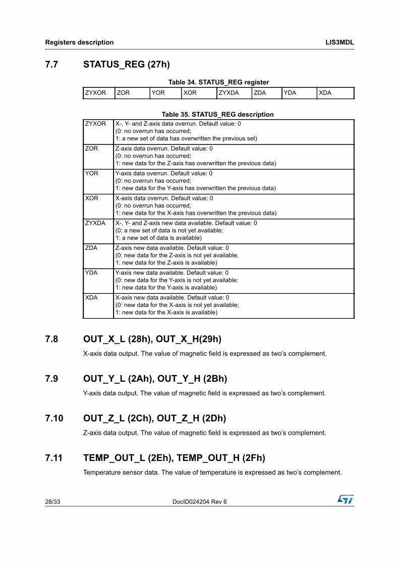
7.7 STATUS_REG (27h)
7.8 OUT_X_L (28h), OUT_X_H(29h)X-axis data output. The value of magnetic field is expressed as two’s complement.
7.9 OUT_Y_L (2Ah), OUT_Y_H (2Bh)Y-axis data output. The value of magnetic field is expressed as two’s complement.
7.10 OUT_Z_L (2Ch), OUT_Z_H (2Dh)Z-axis data output. The value of magnetic field is expressed as two’s complement.
7.11 TEMP_OUT_L (2Eh), TEMP_OUT_H (2Fh) Temperature sensor data. The value of temperature is expressed as two’s complement.
Table 34. STATUS_REG registerZYXOR ZOR YOR XOR ZYXDA ZDA YDA XDA
Table 35. STATUS_REG description ZYXOR X-, Y- and Z-axis data overrun. Default value: 0
(0: no overrun has occurred; 1: a new set of data has overwritten the previous set)
ZOR Z-axis data overrun. Default value: 0(0: no overrun has occurred; 1: new data for the Z-axis has overwritten the previous data)
YOR Y-axis data overrun. Default value: 0(0: no overrun has occurred; 1: new data for the Y-axis has overwritten the previous data)
XOR X-axis data overrun. Default value: 0(0: no overrun has occurred; 1: new data for the X-axis has overwritten the previous data)
ZYXDA X-, Y- and Z-axis new data available. Default value: 0(0: a new set of data is not yet available; 1: a new set of data is available)
ZDA Z-axis new data available. Default value: 0(0: new data for the Z-axis is not yet available; 1: new data for the Z-axis is available)
YDA Y-axis new data available. Default value: 0(0: new data for the Y-axis is not yet available; 1: new data for the Y-axis is available)
XDA X-axis new data available. Default value: 0(0: new data for the X-axis is not yet available; 1: new data for the X-axis is available)

DocID024204 Rev 6 29/33
LIS3MDL Registers description
7.12 INT_CFG (30h)
7.13 INT_SRC (31h)
Table 36. INT_CFG registerXIEN YIEN ZIEN 0(1)
1. This bit must be set to ‘0’ for correct functioning of the device.
1 IEA LIR IEN
Table 37. INT_CFG descriptionXIEN Enable interrupt generation on X-axis. Default value: 1
(0: disable interrupt request; 1: enable interrupt request)YIEN Enable interrupt generation on Y-axis. Default value: 1
(0: disable interrupt request; 1: enable interrupt request)ZIEN Enable interrupt generation on Z-axis. Default value: 1
(0: disable interrupt request; 1: enable interrupt request)IEA Interrupt active configuration on INT. Default value: 0
(0: low; 1: high)LIR Latch interrupt request. Default value: 0
(0: interrupt request latched; 1: interrupt request not latched)Once latched, the INT pin remains in the same state until INT_SRC (31h) is read.
IEN Interrupt enable on INT pin. Default value: 0 (0: disabled; 1: enabled)
Table 38. INT_SRC registerPTH_X PTH_Y PTH_Z NTH_X NTH_Y NTH_Z MROI INT
Table 39. INT_SRC descriptionPTH_X Value on X-axis exceeds the threshold on the positive side.
Default value: 0
PTH_Y Value on Y-axis exceeds the threshold on the positive side. Default value: 0
PTH_Z Value on Z-axis exceeds the threshold on the positive side. Default value: 0
NTH_X Value on X-axis exceeds the threshold on the negative side. Default value: 0
NTH_Y Value on Y-axis exceeds the threshold on the negative side. Default value: 0
NTH_Z Value on Z-axis exceeds the threshold on the negative side. Default value: 0
MROI Internal measurement range overflow on magnetic value. Default value: 0
INT This bit signals when an interrupt event occurs.

Registers description LIS3MDL
30/33 DocID024204 Rev 6
7.14 INT_THS_L(32h), INT_THS_H(33h)Interrupt threshold. Default value: 0.
The value is expressed in 16-bit unsigned.
Even if the threshold is expressed in absolute value, the device detects both positive and negative thresholds.
Table 40. INT_THS_L_M THS7 THS6 THS5 THS4 THS3 THS2 THS1 THS0
Table 41. INT_THS_H_M 0(1)
1. These bits must be set to ‘0’ for correct functioning of the device
THS14 THS13 THS12 THS11 THS10 THS9 THS8

DocID024204 Rev 6 31/33
LIS3MDL Package information
8 Package information
In order to meet environmental requirements, ST offers these devices in different grades of ECOPACK® packages, depending on their level of environmental compliance. ECOPACK® specifications, grade definitions and product status are available at: www.st.com. ECOPACK is an ST trademark.
8.1 VFLGA-12 package information
Figure 12. VFLGA 2x2x1 12LD pitch 0.5 mm package outline
Table 42. VFLGA 2x2x1 12LD pitch 0.5 mm package mechanical data
Dim.mm
Min. Typ. Max.
A1 1
A2 0.785
A3 0.200
D1 1.850 2.000 2.150
E1 1.850 2.000 2.150
L1 1.500
N1 0.500
T1 0.275
T2 0.250
P2 0.075
r 45°
M 0.100
K 0.050
8365767_A

Revision history LIS3MDL
32/33 DocID024204 Rev 6
9 Revision history
Table 43. Document revision history Date Revision Changes
01-Feb-2013 1 Initial release
22-Apr-2013 2Updated note on page 12Product status changed from preliminary data to production data
12-Dec-2014 3
Added FAST_ODR bit to Table 18: CTRL_REG1 register and Table 19: CTRL_REG1 description Added FAST_READ bit to Table 32: CTRL_REG5 register and Table 33: CTRL_REG5 description Updated Table 16: Register address mapMinor textual updates throughout document
15-May-2015 4 Added Table 20: Data rate configuration
28-Oct-2015 5 Updated registers 32h and 33h in Table 16: Register address map
02-May-2017 6Updated Table 1: Device summaryUpdated default values of INT_CFG (30h)

DocID024204 Rev 6 33/33
LIS3MDL
IMPORTANT NOTICE – PLEASE READ CAREFULLY
STMicroelectronics NV and its subsidiaries (“ST”) reserve the right to make changes, corrections, enhancements, modifications, and improvements to ST products and/or to this document at any time without notice. Purchasers should obtain the latest relevant information on ST products before placing orders. ST products are sold pursuant to ST’s terms and conditions of sale in place at the time of order acknowledgement.
Purchasers are solely responsible for the choice, selection, and use of ST products and ST assumes no liability for application assistance or the design of Purchasers’ products.
No license, express or implied, to any intellectual property right is granted by ST herein.
Resale of ST products with provisions different from the information set forth herein shall void any warranty granted by ST for such product.
ST and the ST logo are trademarks of ST. All other product or service names are the property of their respective owners.
Information in this document supersedes and replaces information previously supplied in any prior versions of this document.
© 2017 STMicroelectronics – All rights reserved