Embed Size (px)
Citation preview

EEL7312 – INE5442
Digital Integrated Circuits
1
Digital Integrated Circuits
Chapter 5 - Interconnections

EEL7312 – INE5442
Digital Integrated Circuits
2
Contents
Introduction
Resistance
Capacitance
RC delay
Inductance
Interconnection modeling
Scaling effects on interconnection

EEL7312 – INE5442
Digital Integrated Circuits
3
Introduction - 1
Why are on-chip interconnects important? As technology scales to deep submicron:
Increased contribution to propagation delay Increased contribution on energy dissipation
Introduces extra noise, affects reliability
Trend toward higher integration levels partially driven
by faster, denser, and more reliable on-chip than off-chip interconnects.
Interconnect modeling: resistors, capacitors, and
inductors.

EEL7312 – INE5442
Digital Integrated Circuits
4
Introduction - 2
physical
Source: Rabaey
schematics
transmitters receivers

EEL7312 – INE5442
Digital Integrated Circuits
5
Introduction - 3
Wire Models
All-inclusive modelCapacitance-only
Source: Rabaey
EEL7312 – INE5442
Digital Integrated Circuits
6
Introduction - 4
Source: Weste

EEL7312 – INE5442
Digital Integrated Circuits
7
Introduction - 5
130 nm CMOS technology (Intel)
Transistor
Via
M1
M2
M3
M4
M5
M6
Isolation

EEL7312 – INE5442
Digital Integrated Circuits
8
Resistance - 1
L LR R
H W W
ρ= =
R
: sheet resistance
R1 R2
W
L
H
I
Material
property
Height
Source: Rabaey
Defined by
manufacturer
Defined by
designer
(sometimes)
Ohm’s law
/I V R=
RI
+ V -

EEL7312 – INE5442
Digital Integrated Circuits
9
Resistance - 2
Source: Rabaey

EEL7312 – INE5442
Digital Integrated Circuits
10
Ex: Poly-resistor
L
W
Polysilicon
P substrate
Metal Metal
2 H
LR R R
W= +
R
: sheet resistance
HR : head resistance
Top view
Resistance - 3

EEL7312 – INE5442
Digital Integrated Circuits
11
Resistance - 4
Source: Rabaey
Example: Calculate the approximate resistance of a 1 µm-wide, 1 mm-long wire
of (a) polysilicon; (b) aluminum. Use the data of the above table.
Sheet resistance values for a typical 0.25 µm CMOS process

EEL7312 – INE5442
Digital Integrated Circuits
12
Circuit Simulation - 1
Why using circuit simulators?
Designs can be quickly evaluated without (sometimes very expensive)
fabrication.
After design has been evaluated you can prototype it before mass
production.
A circuit simulator computes the response of the circuit to a particular stimulus.
The simulator formulates the circuit equations and then numerically solves them.
Types of analyses:
DC/DC sweep: Both stimuli and responses do not vary with time
Transient: Responses vary with time
AC/Noise: also called small-signal analysis, it computes the sinusoidal steady-state response
Source: Kundert

EEL7312 – INE5442
Digital Integrated Circuits
13
Circuit Simulation - 2
What are the input data?
Device Type (R, C, L, current sources, voltage sources, diodes,
transistors)
Device models/parameters/ dimensions
How devices are connected
Source: Kundert
Some circuit simulators:
SPICE, PSPICE, HSPICE, Spectre, Smash, SPiceOpus,….

EEL7312 – INE5442
Digital Integrated Circuits
14
Simulation 4.1
Use SpiceOpus to determine the (dc) I-V characteristic of a 1 kΩ resistor.
resistortest
* this is resistortest.cir file
v0 1 0 dc 10V
r1 1 0 1k
.end
r1
I
V0+-
Node 1
Node 0
SpiceOpus (c) 1 -> source resistortest.cir SpiceOpus (c) 2 -> dc v0 -1V 1V 2mV SpiceOpus (c) 3 -> setplot dc1 SpiceOpus (c) 4 -> plot i(v0) xlabel v(1) ylabel current[A] SpiceOpus (c) 5 -> plot -1000*i(v0) xlabel v(1)[V] ylabel current[mA]
V=RI
RI
+ V -

EEL7312 – INE5442
Digital Integrated Circuits
15
Simulation 4.1
r1= 1 kΩ
I
V0+-
Node 1
Node 0
SpiceOpus (c) 5 -> source currentdivider.cir
SpiceOpus (c) 6 -> dc v0 -1 1 5m
SpiceOpus (c) 7 -> setplot dc
SpiceOpus (c) 8 -> plot 1000*i(v1) xlabel v(3)[V] ylabel current[mA]
EEL7312 – INE5442
Digital Integrated Circuits
16
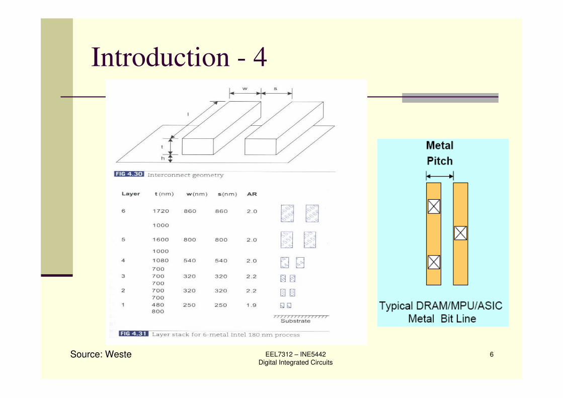
Exercise 4.1 Use SpiceOpus to determine the (dc) I-V0
transfer characteristic of the circuit given below.
r1= r2 =1 kΩ
I
V0+- r1 r2
r3
r3= 0.5 kΩ1V ≥ V0≥ -1V

EEL7312 – INE5442
Digital Integrated Circuits
17
Capacitance - 1
Source: wikipedia
The parallel plate capacitor
Charge separation in a parallel-plate capacitor
causes an internal electric field. A polarized
dielectric spacer (orange) reduces the electric
field and increases the capacitance.
Capacitance: is a measure of the charge
stored on each plate for a given voltage
such that Q=CV
The electric field (force) E between the
plates of a parallel plate capacitor is
uniform and given by E=V/d

EEL7312 – INE5442
Digital Integrated Circuits
18
Capacitance - 2
Source: Rabaey
Dielectric
Substrate
L
W
H
tdi
Electrical-field lines
Current flow
WLt
cdi
diint
ε=
2 fF/µmoxox
ox
Ct
ε=
Defined by foundry

EEL7312 – INE5442
Digital Integrated Circuits
19
Capacitance - 3
Source: Rabaey
material r oε ε ε=128.85 10 F/m
oε −= ⋅
: permittivity of free spaceo
ε

EEL7312 – INE5442
Digital Integrated Circuits
20
Capacitance - Problem
material r oε ε ε=128.85 10 F/m
oε −= ⋅
: permittivity of free spaceo
ε
The distance between the plates of a parallel-plate capacitor
is 10-4 mm. The area of the plates is 1 cm2. Find:
a)The capacitance if the space between the plates is filled
with air
b)The capacitance if the dielectric is SiO2
c)The electric field for 1V voltage difference between the
plates
d)The electric charge Q stored in the SiO2 capacitor for 1V
and the charge density in C/cm2. Give the number of
missing/excess electrons in each plate
Answer
a) C=8.85⋅10-9 F = 8.85 nF
b) εrSiO2= 3.9 ; C=3.9⋅ 8.85=34.5 nF
c) E=107 V/m
d) Q= 34.5 nC; Q/A= 34.5/1=34.5 nC/cm2. N=±Q/q;
N=±21.6 ⋅1010 electrons

EEL7312 – INE5442
Digital Integrated Circuits
21
Capacitance - 4
Source: MOSIS
Fabrication
process
(CMOS)
Gate oxide
thickness
(nm)
Capacitance
/ area
(fF/µm2)
AMIS 1.5
µm
32 1.1
IBM 0.25
µm
6.3 5.5
IBM 0.13
µm
3.2 11
Source: Intel Tech. Journal

EEL7312 – INE5442
Digital Integrated Circuits
22
Capacitance - 5
for constant capacitance
; / ( ) /Q CV I dQ dt d CV dt= = =
/I CdV dt=
+
V
-
I For constant V→ I=0, i.e. a capacitor behaves as an open circuit at
dc.
Capacitors are energy-storage (memory) devices used in filters,
oscillators, power sources, DRAM,…..
Ideal capacitors are not dissipative (and not noisy) but charging and
discharging them causes heating through dissipative devices
connected to the capacitors.

EEL7312 – INE5442
Digital Integrated Circuits
23
The RC circuit - 1
KCL / /C RI CdV dt V R= =
Assume that VS=0 for t<0,
VS=A for t≥0 (and VC(0)=0).
S C RV V V= +KVL
/S C CV RCdV dt V= +
( )1 exp / 0;
0 0
C
C
V A t t
V t
τ= − − ≥
= <
( )/ exp / / 0CI CdV dt A t R tτ= = − ≥
+
VC
-
RI
+ VR -
VS+- C
td=τ ln2≅0.69 τRCτ =
td
50%

EEL7312 – INE5442
Digital Integrated Circuits
24
The RC circuit - 2
Assume that VS=0 for t<0,
VS=A for t≥0 (and VC(0)=0).
( )1 exp /C
V A t τ= − − ( )exp / / 0I A t R tτ= − ≥
The power dissipation p (electric power converted into
heat) in the resistor is
( )2 2 exp 2 / /p RI A t Rτ= = −
The energy converted into heat in the resistor is2 2
0 0
2exp
2R
A t CAE pdt dt
R τ
∞ ∞ = = − =
∫ ∫The energy stored in the capacitor (for t>>τ)
2 2
2 2
CC
CV CAE = =
Exercise: (a) Using the energy conservation principle calculate the energy delivered by
the source. (b) Calculate the energy ES delivered by the source using the formula below
0
S SE V Idt
∞
= ∫
+
VC
-
RI
+ VR -
VS+- C

EEL7312 – INE5442
Digital Integrated Circuits
25
Simulation 4.2
+
VC
-
RI
+ VR -
VS+-
1 2
0
C
RC1
* this is RC1.cir file
v0 1 0 dc 0 pulse 0 1V 0 10ps 10ps 10ns 20ns
R 1 2 1k
C 2 0 1p
.end

EEL7312 – INE5442
Digital Integrated Circuits
26
pulse Vlow Vhigh delay rise fall width period
pulse
v0 1 0 dc 0 pulse 0 1V 0 10ps 10ps 10ns 20ns
Vlow=0
Vhigh=1
delay rise width fall
period0 10ps 10ps10ns
20ns

EEL7312 – INE5442
Digital Integrated Circuits
27
Exercise 4.2 Run SpiceOpus to determine the voltages at the intermediate nodes 2 and 3 for the stimulus of simulation 4.2
R/2I
VS+-
1 2
0C/2
R/2
3
C/2
R= 1 kΩ
C= 1 pF
SpiceOpus (c) 1 -> source RC2.cir SpiceOpus (c) 2 -> tran 0.1ns 20ns
SpiceOpus (c) 3 -> setplot
new New plot
Current tran1RC2 (Transient Analysis)
const Constant values (constants) SpiceOpus (c) 4 -> plot v(1) v(2) v(3) xlabel time[s] ylabel
Outputs[V]
V(3)V(2)

EEL7312 – INE5442
Digital Integrated Circuits
28
Comparison between exercises 4.1 and 4.2
R/2I
VS+-
1 2
0C/2
R/2
3
C/2
R= 1 kΩ
C= 1 pF
RI
VS+-
1 4
0
C
V(4)V(3)

EEL7312 – INE5442
Digital Integrated Circuits
29
Capacitance - 6
Fringing Capacitance
capacitance/unit length
w=W-H/2
W - H/2H
+
(a)
(b)
tdi
substrate
W
H
thick oxide
Source: Rabaey
cfringe
cfringe
cpp
cpp

EEL7312 – INE5442
Digital Integrated Circuits
30
Capacitance - 7
Interwire Capacitance
fringing parallel
Source: Rabaey
Crosstalk: a signal can affect
another nearby signal.
Substrate noise coupling

EEL7312 – INE5442
Digital Integrated Circuits
31
Capacitance - 8
Source: Rabaey
Wiring Capacitances (0.25 µm CMOS)
aF/µm2
aF/µm

EEL7312 – INE5442
Digital Integrated Circuits
32Source: Rabaey
Estimate the capacitance of the wires (with the substrate) specified below:
1. Polysilicon, W= 0.25µm, L=1 mm; 2. Polysilicon, W= 0.25µm, L=10 mm;
3. Metal 1, W= 0.25µm, L=1 mm; 4. Metal 1, W= 0.25µm, L=10 mm.
Exercise 4.3
In each case, calculate the delay time assuming a lumped RC model
for the wire and the capacitance with the substrate. Assume that the
sheet resistances for polysilicon (with silicide) and metal 1 are 5 Ω and
0.1 Ω, respectively.
substrate
W
H
thick oxide
L
; fringePP
PP fringe
CCC WL C L
area length
= =
wire PP fringeC C C= + wire
LR R
W=
0.69d wire wire
t R C≅
288 aF/µm 54 aF/µmfringePP
CC
area length= =

EEL7312 – INE5442
Digital Integrated Circuits
33
1. Cwire=76 fF, Rwire= 20 kΩ, RwireCwire= 1520 ps, td=0.69RwireCwire=1050 ps
Exercise 4.3 - Answer
2. Cwire=760 fF, Rwire= 200 kΩ, RwireCwire= 152 ns, td=0.69RwireCwire=105 ns
3. Cwire=47.5 fF, Rwire= 400 Ω, RwireCwire= 19 ps, td=0.69RwireCwire=13 ps
4. Cwire=475 fF, Rwire= 4 kΩ, RwireCwire= 1.9 ns, td=0.69RwireCwire=1.3 ns
Note that the delay time increases proportionally with the square of the wire length. Why?
So far we have considered that the distributed RC line can be represented by a lumped RC model (pessimistic view) and that the drive signal is a step supplied by an ideal voltage source (optimistic view).

EEL7312 – INE5442
Digital Integrated Circuits
34
RC delay - 1
Vout
Driver
cwire
Vin
Clumped
RdriverVout
Source: Rabaey
Influence of the output resistance of the driver
Rwire<< Rdriver
Example: Rdriver =100 kΩ,
and 1-µm-wide, 10-mm-long Al1 wire. What’s tpd?
230 aF/µm 40 aF/µmfringePP
CC
area length= =
0.3 pF; 0.4 pFfringePP
PP fringe
CCC WL C L
area length
= = = =
0.7 pFwire PP fringeC C C= + =
0.69d driver wire
t R C≅ 50 nsd
t ≅
What’s the approximate maximum operating
frequency of the input such that the output can
detect the correct value of the input?

EEL7312 – INE5442
Digital Integrated Circuits
35
RC delay – 2: The Elmore delay -1
Sources: Rabaey & *W. C. Elmore, “The transient response
of damped linear networks with particular regard to wideband amplifiers,” J. Applied Physics, vol. 19, Jan 1948
Elmore delay model *– method to determine the approximate delay time in an RC
network; it avoids running costly simulations for calculation of delay time. Useful for
determining delays in transmission lines, gates, clock distribution networks,…

EEL7312 – INE5442
Digital Integrated Circuits
36Source: Rabaey
path s→i Rii=R1+R3+Ri
path s→1 Ri1=R1
path s→2 Ri2=R1
path s→3 Ri3=R1+R3
path s→4 Ri4=R1+R3
RC delay – 3: The Elmore delay -2
( )
( )( )
1 1 2 2 3 3 4 4
1 3
1 1
1 2
1 3 3
1 3 4
Di i i i i ii i
i i
R C R C R C R C R C
R R R C
R C
R C
R R C
R R C
τ = + + + + =
+ + +
+
+
+ +
+ +

EEL7312 – INE5442
Digital Integrated Circuits
37
RC delay – 4: The Elmore delay - 3
Let R, C, and l be the total line resistance, capacitance, and length.
Application of the Elmore delay formula to a (RC) wire.
/ ; / ; /r R l c C l L l N= = ∆ =
( ) ( ) ( )
( )
2
1
2 2
1 2 ....
1 1 /
2 2
N
Dout
i
ir L c L rc L N
N Nrc l N N rcl
N
τ=
= ∆ ∆ = ∆ + + + =
+ +=
∑2
2 1lim
2 2 2Dout
N
N rcl RCrcl
Nτ
→∞
+= = =
The delay of a wire is proportional
to the square of its length. Note: The Elmore formula applied to the
RC lumped model gives τDout=RC
Source: Rabaey

EEL7312 – INE5442
Digital Integrated Circuits
38
RC delay – 5: The Elmore delay - 4
Example 4.8 of Rabaey’s book: 10-cm-long, 1- µm-wide Al1 wire
for which r=0.075 Ω/ µm, c= 110 aF/µm.
( )22 5/ 2 0.075 /µm 110aF/µm 10 µm / 2 41.3 ns
Doutrclτ = = Ω ⋅ ⋅ =
Note: The Elmore delay is, in general, not equal to the delay time. For
a distributed RC network, the Elmore delay τD = 0.5 RC whereas the delay time td = 0.38 RC
Source: Rabaey

EEL7312 – INE5442
Digital Integrated Circuits
39
RC delay – 6Example 4.8 of Rabaey’s book: 10-cm-
long, 1- µm-wide Al1 wire for which
r=0.075 Ω/ µm, c= 110 aF/µm.
Distributed RC line 1
* this is DistributedRCline.cir file
v0 1 0 dc 0 pulse 0 1V 0 10ps 10ps 200ns 400ns
URC1 1 2 0 MURC L=100m
.model MURC URC rperl=75k cperl=110p
.end
SpiceOpus (c) 7 -> source DistributedRCline.cir
SpiceOpus (c) 8 -> tran 1ns 200ns
SpiceOpus (c) 9 -> setplot
new New plot
Current tran2 Distributed RC line 1 (Transient Analysis)
SpiceOpus (c) 10 -> setplot tran2
SpiceOpus (c) 11 -> plot v(2) xlabel time ylabel Vout
lumped
distributed

EEL7312 – INE5442
Digital Integrated Circuits
40
RC delay – 7
Diffusion equation
Source: Rabaey

EEL7312 – INE5442
Digital Integrated Circuits
41
RC delay – 8
Step-response of RC wire as a function of time and space
Source: Rabaey
0 0.5 1 1.5 2 2.5 3 3.5 4 4.5 50
0.5
1
1.5
2
2.5
time (nsec)
vo
lta
ge
(V
)
x= L/10
x = L/4
x = L/2
x= L

EEL7312 – INE5442
Digital Integrated Circuits
42
RC delay – 9
Voltage range Lumped RC network Distributed RC network
0→50% (tp) 0.69 RC 0.38 RC
0→63% (τ) RC 0.5 RC
10→90% (tr) 2.2 RC 0.9 RC
Source: Rabaey

EEL7312 – INE5442
Digital Integrated Circuits
43
RC delay – 10
Source: Rabaey
Vout
Driver
cwire
VinC
Rdriver
Vout
L
rw, cw, L
When are the effects of the
wire delay important?
Assume that the driver delay
is tpgate. The wire delay is 2
0.38 0.38pwire w wt RC r c L= =
The wire delay is important when
tpwire≅tpgate or, equivalently
0.38
pgate
crit
w w
tL
r c=

EEL7312 – INE5442
Digital Integrated Circuits
44
RC delay – 11Example 4.8 of Rabaey’s book: 10-cm-
long, 1- µm-wide Al1 wire for which
r=0.075 Ω/ µm, c= 110 aF/µm.
Distributed RC line 2
* this is DistributedRCline2.cir
*file
* the rise time is of the order of the
*RC time constant
v0 1 0 dc 0 pulse 0 1V 0 50ns 50ns
+200ns 500ns
URC1 1 2 0 MURC L=100m
.model MURC URC K=2
+fmax=20G rperl=75k cperl=110p
.end
Response to pulse
rise time=0
Response to pulse
rise time=50 ns
Note that the internal resistance of the
voltage source is zero in this example
What if the rise time becomes much higher than RC?

EEL7312 – INE5442
Digital Integrated Circuits
45
RC delay – 12Example 4.8 of Rabaey’s book: 10-cm-
long, 1- µm-wide Al1 wire for which
r=0.075 Ω/ µm, c= 110 aF/µm.
What if the rise time becomes much higher than RC?

EEL7312 – INE5442
Digital Integrated Circuits
46
RC delay – 13
Source: Weste&Harris

EEL7312 – INE5442
Digital Integrated Circuits
47
RC delay – 14
Source: Rabaey
Design Rules of Thumb
rc delays should only be considered when tpRC >> tpgate of the driving gate
Lcrit >> √ tpgate/0.38rc
rc delays should only be considered when the rise (fall) time at the line input is smaller than RC, the rise (fall) time of the line
trise < RC when not met, the change in the signal is slower than
the propagation delay of the wire

EEL7312 – INE5442
Digital Integrated Circuits
48
I
+ VL -
Inductance - 1
/LV LdI dt=2 / 2LE LI=
Inductive effects
important for power grids (high current), clock networks
(high speed), and wide busses (low resistance/unit length);
may cause ringing/overshoot effects, reflection of signals,
inductive coupling between lines (crosstalk), and switching
noise in power lines
Clock trees and power/ground grid need to be designed carefully to avoid large clock skew, signal inductive coupling and ground bounce

EEL7312 – INE5442
Digital Integrated Circuits
49
Inductance - 2
Inductance of a wire depends on its geometry and surrounding dielectric
Extracting the inductance is in general a 3-D problem and is extremely time-consuming for complex geometries
Inductance depends on the entire current loop; it is impractical to extract the inductance from a chip layout
Source: Rabaey,
Weste&Harris

EEL7312 – INE5442
Digital Integrated Circuits
50
Inductance - 3
The Wave Equation
V in Voutr
c
r r x
c
r
c c
l l l l
The Transmission Line
Source: Rabaey
When r=0 →→→→ signal travels at speed of light, which is smaller than speed of light in vacuum (300 mm/ns). In the real case, currents return in distant power lines and
increase inductance thus reducing signal velocity.
When l=0 →→→→ rc wire (diffusion equation)

EEL7312 – INE5442
Digital Integrated Circuits
51
Inductance - 4
IEEE JSSC, vol. 37, no. 6, June 2002
High-frequency characterization of on-chip digital interconnects
Kleveland, B.; Xiaoning Qi; Madden, L.; Furusawa, T.; Dutton, R.W.;
Horowitz, M.A.; Wong, S.S.
Page(s): 716-725

EEL7312 – INE5442
Digital Integrated Circuits
52
Inductance - 5
Source: Qi, CICC 2000

EEL7312 – INE5442
Digital Integrated Circuits
53
Crosstalk is the coupling of energy from one line to another via:
Mutual capacitance (electric field)
Mutual inductance (magnetic field)
Mutual Capacitance, Cm Mutual Inductance, Lm
Source: Intel
Zs
Zo
Zo
Zo
Zs
Zo
Zo
Zo
Cm
Lm
near
far
near
far
Crosstalk

EEL7312 – INE5442
Digital Integrated Circuits
54
Scaling effects on interconnection
Rabaey’s book pages 170-174
Weste & Harris, pages 249-250
Interconnect Scaling, Prof. Krishna Saraswat,
On line available
http://www.stanford.edu/class/ee311/NOTES/InterconnectScalingSlides.pdf