Embed Size (px)
Citation preview
This is information on a product in full production.
September 2013 DocID022674 Rev 4 1/48
1
TDA7801
Digital input quad power amplifier with built-in diagnostics features
Datasheet - production data
Features
Integrated 110 dB D/A conversion
I2S digital input (3.3/1.8 V) with TDM option
Selectable input sampling frequency: 44.1 kHz, 48 kHz, 96 kHz, 192 kHz
MOSFET power outputs
High output power capability 4x28 W/ 4 @ 14.4 V, 1 kHz, 10 % THD
Max. output power 4x72 W/2
Full I2C bus driving (3.3/5 V):
– Independent front/rear soft play/ mute
– Selectable gain (four levels) for very low noise line-out function
– I2C bus digital diagnostics (including DC and AC load detection)
Two I2C bus addresses and 8-ch TDM mode (only in PowerSO package)
Optional non I2C bus mode
Offset detector (play or mute mode)
Clipping detector (selectable level) and diagnostics pin
CMOS compatible enable pin (3.3/5 V)
Full fault protection
Four independent short circuit protections
Linear thermal protection (four thermal warnings)
ESD protection
Description
The TDA7801 is a new BCD technology quad bridge amplifier for car audio applications.
Thanks to the BCD6 technology it is possible to integrate a high performance D/A converter together with powerful MOSFET outputs.
The possibility of having the D/A conversion on board allows the performance to reach an outstanding 115 dB S/N ratio with more than 105 dB of dynamic range.
This device is equipped with a full diagnostics array that communicates the status of each speaker through the I2C bus. The possibility to control the configuration and behavior of the device by means of the I2C bus makes TDA7801 a very flexible machine.
PowerSO36
Flexiwatt27(vertical)
Flexiwatt27(SMD)
(slug-up) Flexiwatt27(horizontal)
Table 1. Device summary
Order code Package Packing
TDA7801PD PowerSO36 (slug-up) Tube
TDA7801PDTR PowerSO36 (slug-up) Tape and reel
TDA7801 Flexiwatt27 (vertical) Tube
TDA7801H Flexiwatt27 (horizontal) Tube
TDA7801SM Flexiwatt27 (SMD) Tube
www.st.com

Contents TDA7801
2/48 DocID022674 Rev 4
Contents
1 Block diagram and pins description . . . . . . . . . . . . . . . . . . . . . . . . . . . . 6
1.1 Block diagram . . . . . . . . . . . . . . . . . . . . . . . . . . . . . . . . . . . . . . . . . . . . . . . 6
2 Application diagrams . . . . . . . . . . . . . . . . . . . . . . . . . . . . . . . . . . . . . . . . 7
2.1 Pin description . . . . . . . . . . . . . . . . . . . . . . . . . . . . . . . . . . . . . . . . . . . . . . 9
3 Electrical specifications . . . . . . . . . . . . . . . . . . . . . . . . . . . . . . . . . . . . . 12
3.1 Absolute maximum ratings . . . . . . . . . . . . . . . . . . . . . . . . . . . . . . . . . . . . 12
3.2 Thermal data . . . . . . . . . . . . . . . . . . . . . . . . . . . . . . . . . . . . . . . . . . . . . . 12
3.3 Electrical characteristics . . . . . . . . . . . . . . . . . . . . . . . . . . . . . . . . . . . . . . 13
3.4 Electrical characteristics typical curves . . . . . . . . . . . . . . . . . . . . . . . . . . 17
4 Operation mode . . . . . . . . . . . . . . . . . . . . . . . . . . . . . . . . . . . . . . . . . . . . 21
4.1 Standby mode . . . . . . . . . . . . . . . . . . . . . . . . . . . . . . . . . . . . . . . . . . . . . 21
4.2 Tristate mode . . . . . . . . . . . . . . . . . . . . . . . . . . . . . . . . . . . . . . . . . . . . . . 21
4.3 Amplifier mode . . . . . . . . . . . . . . . . . . . . . . . . . . . . . . . . . . . . . . . . . . . . . 21
5 "PLL-filter /enable" pin description . . . . . . . . . . . . . . . . . . . . . . . . . . . . 22
5.1 Functionality . . . . . . . . . . . . . . . . . . . . . . . . . . . . . . . . . . . . . . . . . . . . . . . 22
5.2 Driving . . . . . . . . . . . . . . . . . . . . . . . . . . . . . . . . . . . . . . . . . . . . . . . . . . . 22
6 Functional description . . . . . . . . . . . . . . . . . . . . . . . . . . . . . . . . . . . . . . 23
6.1 Voltage supplies timing . . . . . . . . . . . . . . . . . . . . . . . . . . . . . . . . . . . . . . . 23
6.2 Turn-on diagnostic description . . . . . . . . . . . . . . . . . . . . . . . . . . . . . . . . . 23
6.3 Permanent diagnostic . . . . . . . . . . . . . . . . . . . . . . . . . . . . . . . . . . . . . . . . 25
6.4 AC diagnostic . . . . . . . . . . . . . . . . . . . . . . . . . . . . . . . . . . . . . . . . . . . . . . 26
6.5 Output DC offset detection . . . . . . . . . . . . . . . . . . . . . . . . . . . . . . . . . . . . 26
6.6 Multiple faults . . . . . . . . . . . . . . . . . . . . . . . . . . . . . . . . . . . . . . . . . . . . . . 27
6.7 Faults availability . . . . . . . . . . . . . . . . . . . . . . . . . . . . . . . . . . . . . . . . . . . 27
6.8 I2C programming/reading sequence . . . . . . . . . . . . . . . . . . . . . . . . . . . . 27
6.9 Legacy mode . . . . . . . . . . . . . . . . . . . . . . . . . . . . . . . . . . . . . . . . . . . . . . 28
6.10 Thermal protection . . . . . . . . . . . . . . . . . . . . . . . . . . . . . . . . . . . . . . . . . . 28

DocID022674 Rev 4 3/48
TDA7801 Contents
6.11 Under-voltage threshold . . . . . . . . . . . . . . . . . . . . . . . . . . . . . . . . . . . . . . 29
6.11.1 Supply voltage auto-mute threshold . . . . . . . . . . . . . . . . . . . . . . . . . . . 29
6.11.2 Digital mute disabling . . . . . . . . . . . . . . . . . . . . . . . . . . . . . . . . . . . . . . . 29
6.11.3 Power-on reset threshold . . . . . . . . . . . . . . . . . . . . . . . . . . . . . . . . . . . . 29
6.12 Fast mute features . . . . . . . . . . . . . . . . . . . . . . . . . . . . . . . . . . . . . . . . . . 30
7 I2S bus interface . . . . . . . . . . . . . . . . . . . . . . . . . . . . . . . . . . . . . . . . . . . 31
7.1 Interface timings requirements . . . . . . . . . . . . . . . . . . . . . . . . . . . . . . . . . 32
7.2 Group delay . . . . . . . . . . . . . . . . . . . . . . . . . . . . . . . . . . . . . . . . . . . . . . . 33
8 I2C bus interface . . . . . . . . . . . . . . . . . . . . . . . . . . . . . . . . . . . . . . . . . . . 34
8.1 Writing procedure . . . . . . . . . . . . . . . . . . . . . . . . . . . . . . . . . . . . . . . . . . . 35
8.2 Reading procedure . . . . . . . . . . . . . . . . . . . . . . . . . . . . . . . . . . . . . . . . . . 35
8.3 Data validity . . . . . . . . . . . . . . . . . . . . . . . . . . . . . . . . . . . . . . . . . . . . . . . 35
8.4 Start and stop conditions . . . . . . . . . . . . . . . . . . . . . . . . . . . . . . . . . . . . . 35
8.5 Byte format . . . . . . . . . . . . . . . . . . . . . . . . . . . . . . . . . . . . . . . . . . . . . . . . 35
8.6 Acknowledge . . . . . . . . . . . . . . . . . . . . . . . . . . . . . . . . . . . . . . . . . . . . . . 35
9 I2C registers . . . . . . . . . . . . . . . . . . . . . . . . . . . . . . . . . . . . . . . . . . . . . . . 36
9.1 IB0-Addr:"00000" . . . . . . . . . . . . . . . . . . . . . . . . . . . . . . . . . . . . . . . . . . . 36
9.2 IB1-Addr:"00001" . . . . . . . . . . . . . . . . . . . . . . . . . . . . . . . . . . . . . . . . . . . 36
9.3 IB2-Addr:"00010" . . . . . . . . . . . . . . . . . . . . . . . . . . . . . . . . . . . . . . . . . . . 37
9.4 IB3-Addr:"00011" . . . . . . . . . . . . . . . . . . . . . . . . . . . . . . . . . . . . . . . . . . . 38
9.5 IB4-Addr:"00100" . . . . . . . . . . . . . . . . . . . . . . . . . . . . . . . . . . . . . . . . . . . 38
9.6 DB0-Addr:"10000" - Channel 1 (left front) . . . . . . . . . . . . . . . . . . . . . . . . 39
9.7 DB1-Addr:"10001" - Channel 2 (left rear) . . . . . . . . . . . . . . . . . . . . . . . . . 40
9.8 DB2-Addr:"10010"" - Channel 3 (right front) . . . . . . . . . . . . . . . . . . . . . . 41
9.9 DB3-Addr:"10011" - Channel 4 (right rear) . . . . . . . . . . . . . . . . . . . . . . . . 42
9.10 DB4-Addr:"10100" . . . . . . . . . . . . . . . . . . . . . . . . . . . . . . . . . . . . . . . . . . 42
10 Package information . . . . . . . . . . . . . . . . . . . . . . . . . . . . . . . . . . . . . . . . 43
11 Revision history . . . . . . . . . . . . . . . . . . . . . . . . . . . . . . . . . . . . . . . . . . . 47

List of tables TDA7801
4/48 DocID022674 Rev 4
List of tables
Table 1. Device summary . . . . . . . . . . . . . . . . . . . . . . . . . . . . . . . . . . . . . . . . . . . . . . . . . . . . . . . . . . 1Table 2. Flexiwatt27 (vertical/SMD/horizontal) pin description . . . . . . . . . . . . . . . . . . . . . . . . . . . . . 10Table 3. PowerSO36 pin description . . . . . . . . . . . . . . . . . . . . . . . . . . . . . . . . . . . . . . . . . . . . . . . . 11Table 4. Absolute maximum ratings . . . . . . . . . . . . . . . . . . . . . . . . . . . . . . . . . . . . . . . . . . . . . . . . . 12Table 5. Thermal data. . . . . . . . . . . . . . . . . . . . . . . . . . . . . . . . . . . . . . . . . . . . . . . . . . . . . . . . . . . . 12Table 6. Electrical characteristics . . . . . . . . . . . . . . . . . . . . . . . . . . . . . . . . . . . . . . . . . . . . . . . . . . . 13Table 7. Start-up diagnostic pulse typical timing . . . . . . . . . . . . . . . . . . . . . . . . . . . . . . . . . . . . . . . 24Table 8. Multiple faults priority . . . . . . . . . . . . . . . . . . . . . . . . . . . . . . . . . . . . . . . . . . . . . . . . . . . . . 27Table 9. System clock frequencies for common audio sampling frequencies . . . . . . . . . . . . . . . . . 32Table 10. Example timing for tck = 1/fSCK, where fSCK is stated in the Table 9 . . . . . . . . . . . . . . . . . 33Table 11. IB0-Addr:"00000" . . . . . . . . . . . . . . . . . . . . . . . . . . . . . . . . . . . . . . . . . . . . . . . . . . . . . . . . 36Table 12. IB1-Addr:"00001" . . . . . . . . . . . . . . . . . . . . . . . . . . . . . . . . . . . . . . . . . . . . . . . . . . . . . . . . 36Table 13. IB3-Addr:"00010" . . . . . . . . . . . . . . . . . . . . . . . . . . . . . . . . . . . . . . . . . . . . . . . . . . . . . . . . 37Table 14. IB3-Addr:"00011" . . . . . . . . . . . . . . . . . . . . . . . . . . . . . . . . . . . . . . . . . . . . . . . . . . . . . . . . 38Table 15. IB4-Addr:"00100" . . . . . . . . . . . . . . . . . . . . . . . . . . . . . . . . . . . . . . . . . . . . . . . . . . . . . . . . 38Table 16. DB0-Addr:"10000" - Channel 1 (left front). . . . . . . . . . . . . . . . . . . . . . . . . . . . . . . . . . . . . . 39Table 17. DB1-Addr:"10001" - Channel 2 (left rear) . . . . . . . . . . . . . . . . . . . . . . . . . . . . . . . . . . . . . . 40Table 18. DB2-Addr:"10010"" - Channel 3 (right front) . . . . . . . . . . . . . . . . . . . . . . . . . . . . . . . . . . . . 41Table 19. DB3-Addr:"10011" - Channel 4 (right rear) . . . . . . . . . . . . . . . . . . . . . . . . . . . . . . . . . . . . . 42Table 20. DB4-Addr:"10100". . . . . . . . . . . . . . . . . . . . . . . . . . . . . . . . . . . . . . . . . . . . . . . . . . . . . . . . 42Table 21. Document revision history . . . . . . . . . . . . . . . . . . . . . . . . . . . . . . . . . . . . . . . . . . . . . . . . . 47

DocID022674 Rev 4 5/48
TDA7801 List of figures
List of figures
Figure 1. Block diagram (Flexiwatt27) . . . . . . . . . . . . . . . . . . . . . . . . . . . . . . . . . . . . . . . . . . . . . . . . . 6Figure 2. I2C bus mode application diagram (TDA7801/H/SM) . . . . . . . . . . . . . . . . . . . . . . . . . . . . . . 7Figure 3. I2C bus mode application diagram (TDA7801PD) . . . . . . . . . . . . . . . . . . . . . . . . . . . . . . . . 7Figure 4. Legacy mode application diagram (TDA7801/H/SM) . . . . . . . . . . . . . . . . . . . . . . . . . . . . . . 8Figure 5. Legacy mode application diagram (TDA7801PD) . . . . . . . . . . . . . . . . . . . . . . . . . . . . . . . . 8Figure 6. Pin connection diagrams . . . . . . . . . . . . . . . . . . . . . . . . . . . . . . . . . . . . . . . . . . . . . . . . . . . 9Figure 7. Quiescent current vs. supply voltage . . . . . . . . . . . . . . . . . . . . . . . . . . . . . . . . . . . . . . . . . 17Figure 8. Output power vs. supply voltage (4 ) . . . . . . . . . . . . . . . . . . . . . . . . . . . . . . . . . . . . . . . . 17Figure 9. Output power vs. supply voltage (2 ) . . . . . . . . . . . . . . . . . . . . . . . . . . . . . . . . . . . . . . . . 17Figure 10. Distortion vs. output power (4 ) . . . . . . . . . . . . . . . . . . . . . . . . . . . . . . . . . . . . . . . . . . . . 17Figure 11. Distortion vs. output power (2 ) . . . . . . . . . . . . . . . . . . . . . . . . . . . . . . . . . . . . . . . . . . . . 18Figure 12. Distortion vs. frequency (4 ) . . . . . . . . . . . . . . . . . . . . . . . . . . . . . . . . . . . . . . . . . . . . . . . 18Figure 13. Distortion vs. frequency (2 ) . . . . . . . . . . . . . . . . . . . . . . . . . . . . . . . . . . . . . . . . . . . . . . . 18Figure 14. Vo vs. Vin (Gv1-2-3-4 settings). . . . . . . . . . . . . . . . . . . . . . . . . . . . . . . . . . . . . . . . . . . . . . 18Figure 15. Vo vs. Vin (Gv1-2-3-4 settings + 6 dB dig. gain). . . . . . . . . . . . . . . . . . . . . . . . . . . . . . . . . 18Figure 16. Distortion vs. output voltage (LD-Gv2) . . . . . . . . . . . . . . . . . . . . . . . . . . . . . . . . . . . . . . . . 18Figure 17. Distortion vs. output voltage (LD-Gv3) . . . . . . . . . . . . . . . . . . . . . . . . . . . . . . . . . . . . . . . . 19Figure 18. Distortion vs. output voltage (LD-Gv4) . . . . . . . . . . . . . . . . . . . . . . . . . . . . . . . . . . . . . . . . 19Figure 19. Output attenuation vs. Vs . . . . . . . . . . . . . . . . . . . . . . . . . . . . . . . . . . . . . . . . . . . . . . . . . . 19Figure 20. Crosstalk vs. frequency . . . . . . . . . . . . . . . . . . . . . . . . . . . . . . . . . . . . . . . . . . . . . . . . . . . 19Figure 21. Supply voltage rejection vs. frequency . . . . . . . . . . . . . . . . . . . . . . . . . . . . . . . . . . . . . . . . 19Figure 22. Total power dissipation & efficiency vs. Po (4 ) . . . . . . . . . . . . . . . . . . . . . . . . . . . . . . . . 19Figure 23. Power dissipation vs. average Po (audio program simulation, 4 ) . . . . . . . . . . . . . . . . . . 20Figure 24. Power dissipation vs. average Po (audio program simulation, 2 ) . . . . . . . . . . . . . . . . . . 20Figure 25. ITU R-ARM frequency response, weighting filter for transient pop. . . . . . . . . . . . . . . . . . . 20Figure 26. Standby driving circuit. . . . . . . . . . . . . . . . . . . . . . . . . . . . . . . . . . . . . . . . . . . . . . . . . . . . . 22Figure 27. Turn-on diagnostic cycle. Positive and negative output behaviour . . . . . . . . . . . . . . . . . . . 23Figure 28. Turn-on diag. cycle with transition in amp. mode. Positive and negative output behaviour 24Figure 29. Short to GND and short to Vs, threshold description . . . . . . . . . . . . . . . . . . . . . . . . . . . . . 25Figure 30. Short across the speaker and open load threshold description, in amplifier mode. . . . . . . 25Figure 31. Short across the speaker and open load threshold description, in line driver mode. . . . . . 25Figure 32. Thermal muting diagram. . . . . . . . . . . . . . . . . . . . . . . . . . . . . . . . . . . . . . . . . . . . . . . . . . . 28Figure 33. Low voltage mute attenuation, supply voltage variation (Vs); result digital attenuation (At)29Figure 34. TDM setting . . . . . . . . . . . . . . . . . . . . . . . . . . . . . . . . . . . . . . . . . . . . . . . . . . . . . . . . . . . . 31Figure 35. I2S format . . . . . . . . . . . . . . . . . . . . . . . . . . . . . . . . . . . . . . . . . . . . . . . . . . . . . . . . . . . . . . 31Figure 36. Audio data input format. . . . . . . . . . . . . . . . . . . . . . . . . . . . . . . . . . . . . . . . . . . . . . . . . . . . 32Figure 37. Audio interface timing . . . . . . . . . . . . . . . . . . . . . . . . . . . . . . . . . . . . . . . . . . . . . . . . . . . . . 32Figure 38. I2C bus protocol description . . . . . . . . . . . . . . . . . . . . . . . . . . . . . . . . . . . . . . . . . . . . . . . . 34Figure 39. PowerSO36 (slug-up) mechanical data and package dimensions . . . . . . . . . . . . . . . . . . . 43Figure 40. Flexiwatt27 (vertical) mechanical data and package dimensions. . . . . . . . . . . . . . . . . . . . 44Figure 41. Flexiwatt27 (horizontal) mechanical data and package dimensions. . . . . . . . . . . . . . . . . . 45Figure 42. Flexiwatt27 (SMD) mechanical data and package dimensions . . . . . . . . . . . . . . . . . . . . . 46
Block diagram and pins description TDA7801
6/48 DocID022674 Rev 4
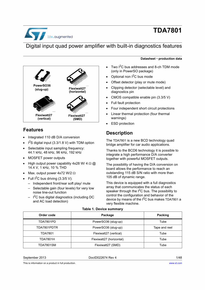
1 Block diagram and pins description
1.1 Block diagram
Figure 1. Block diagram (Flexiwatt27)

DocID022674 Rev 4 7/48
TDA7801 Application diagrams
2 Application diagrams
Figure 2. I2C bus mode application diagram (TDA7801/H/SM)
Figure 3. I2C bus mode application diagram (TDA7801PD)

Application diagrams TDA7801
8/48 DocID022674 Rev 4
Figure 4. Legacy mode application diagram (TDA7801/H/SM)
Figure 5. Legacy mode application diagram (TDA7801PD)

DocID022674 Rev 4 9/48
TDA7801 Application diagrams
2.1 Pin description
Figure 6. Pin connection diagrams

Application diagrams TDA7801
10/48 DocID022674 Rev 4
Table 2. Flexiwatt27 (vertical/SMD/horizontal) pin description
N° Pin Function
1 TAB TAB connection (GND)
2 Pll-filter / ENABLE Pll loop filter / ENABLE
3 PW_GND Power ground channel 2
4 OUT 2- / LR- Channel 2 (Left Rear) negative output
5 WS Word select (I2S bus, logic input)
6 OUT 2+ / LR+ Channel 2 (Left Rear) positive output
7 Vcc Channel 1 and 2 positive supply
8 OUT 1- / LF- Channel 1 (Left Front) negative output
9 PW_GND Power ground channel 1
10 OUT 1+ / LF+ Channel 1 (Left Front) positive output
11 SCK Serial clock (I2S bus, logic input)
12 SD2_4 Serial data channels 2 and 4 (I2S bus, logic input)
13 SD1_3 Serial data channels 1 and 3 (I2S bus, logic input)
14 Dgnd Digital ground
15 Agnd Analog ground
16 D3V Digital 3.3 V supply filter
17 A3V Analog 3.3 V supply filter
18 OUT3+ / RF+ Channel 3 (right front) positive output
19 PW_GND Power ground channel 3
20 OUT3- / RF- Channel 3 (right front) negative output
21 Vcc Channels 3 and 4 positive supply
22 OUT4+ / RR+ Channel 4 (right rear) positive output
23 CD/DIAG
Clip detector and diagnostic output:
– Overcurrent protection intervention
– Thermal warning– POR
– (Open drain output)
24 OUT4- / RR- Channel 4 (right rear) negative output
25 PW_GND Power ground channel 4
26 I2C Data I2C data/legacy mode mute
27 I2C Clock I2C clock/enable legacy mode

DocID022674 Rev 4 11/48
TDA7801 Application diagrams
Table 3. PowerSO36 pin description
N° Pin Function
1 TAB TAB connection (GND)
2 CD/DIAG
Clip detector and diagnostic output:
Overcurrent protection interventionThermal warningOffset detectionPOR (Open drain output)
3 OUT4- Channel 4 (right rear) negative output
4 VCC Channels 3-4 positive supply
5 PW_GND Power ground channel 4
6 VCC Channels 3-4 positive supply
7 OUT4+ Channel 4 (right rear) positive output
8 I2C Data I2C Data / legacy mode mute
9 I2C Clock I2C Clock / enable legacy mode
10 I2C Address I2C Address
11 Pll loop
filter/Enable Pll loop filter / Enable
12 OUT2+ Channel 2 (left rear) positive output
13 VCC Channel 1-2 positive supply
14 NC Not connected
15 PW_GND Power ground channel 2
16 VCC Channel 1-2 positive supply
17 OUT2- Channel 2 (left rear) negative output
18 WS Word Select (I2S bus, logic input)
19 OUT1- Channel 1 (left front) negative output
20 NC Not connected
21 NC Not connected
22 PW_GND Power ground channel 1
23 OUT1+ Channel 1 (left front) positive output
24 NC Not connected
25 SCK Serial clock (I2S bus, logic input)
26 SD2_4 Serial data channels 2 and 4 (I2S bus, logic input)
27 SD1_3 Serial data channels 1 and 3 (I2S bus, logic input)
28 Dgnd Digital ground
29 Agnd Analog ground
30 D3V Digital 3.3 V supply filter
31 A3V Analog 3.3 V supply filter
32 OUT3+ Channel 3 (right front) positive output
33 PW_GND Power ground channel 3
34 NC Not connected
35 NC Not connected
36 OUT3- Channel 3 (right front) negative output
Electrical specifications TDA7801
12/48 DocID022674 Rev 4
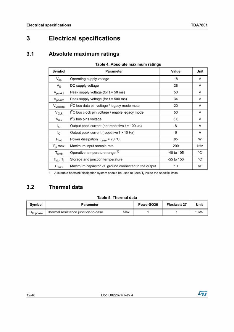
3 Electrical specifications
3.1 Absolute maximum ratings
3.2 Thermal data
Table 4. Absolute maximum ratings
Symbol Parameter Value Unit
Vop Operating supply voltage 18 V
VS DC supply voltage 28 V
Vpeak1 Peak supply voltage (for t = 50 ms) 50 V
Vpeak2 Peak supply voltage (for t = 500 ms) 34 V
Vi2cdata I2C bus data pin voltage / legacy mode mute 20 V
Vi2ck I2C bus clock pin voltage / enable legacy mode 50 V
Vi2s I2S bus pins voltage 3.6 V
IO Output peak current (not repetitive t = 100 µs) 8 A
IO Output peak current (repetitive f > 10 Hz) 6 A
Ptot Power dissipation Tcase = 70 °C 85 W
Fs max Maximum input sample rate 200 kHz
Tamb Operative temperature range(1)
1. A suitable heatsink/dissipation system should be used to keep Tj inside the specific limits.
-40 to 105 °C
Tstg, Tj Storage and junction temperature -55 to 150 °C
Cmax Maximum capacitor vs. ground connected to the output 10 nF
Table 5. Thermal data
Symbol Parameter PowerSO36 Flexiwatt 27 Unit
Rth j-case Thermal resistance junction-to-case Max 1 1 °C/W
DocID022674 Rev 4 13/48
TDA7801 Electrical specifications
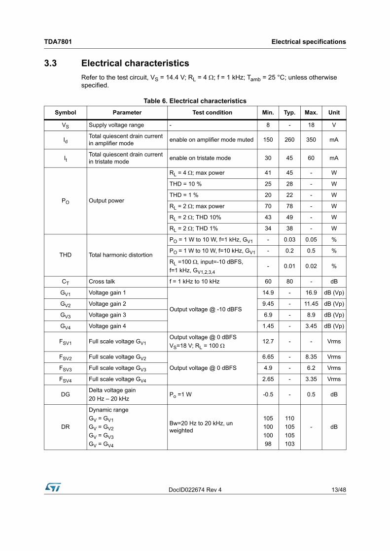
3.3 Electrical characteristics
Refer to the test circuit, VS = 14.4 V; RL = 4 ; f = 1 kHz; Tamb = 25 °C; unless otherwise specified.
Table 6. Electrical characteristics
Symbol Parameter Test condition Min. Typ. Max. Unit
VS Supply voltage range - 8 - 18 V
IdTotal quiescent drain current in amplifier mode
enable on amplifier mode muted 150 260 350 mA
ItTotal quiescent drain current in tristate mode
enable on tristate mode 30 45 60 mA
PO Output power
RL = 4 ; max power 41 45 - W
THD = 10 % 25 28 - W
THD = 1 % 20 22 - W
RL = 2 ; max power 70 78 - W
RL = 2 ; THD 10% 43 49 - W
RL = 2 ; THD 1% 34 38 - W
THD Total harmonic distortion
PO = 1 W to 10 W, f=1 kHz, GV1 - 0.03 0.05 %
PO = 1 W to 10 W, f=10 kHz, GV1 - 0.2 0.5 %
RL =100 input=-10 dBFS,
f=1 kHz, GV1,2,3,4- 0.01 0.02 %
CT Cross talk f = 1 kHz to 10 kHz 60 80 - dB
GV1 Voltage gain 1
Output voltage @ -10 dBFS
14.9 - 16.9 dB (Vp)
GV2 Voltage gain 2 9.45 - 11.45 dB (Vp)
GV3 Voltage gain 3 6.9 - 8.9 dB (Vp)
GV4 Voltage gain 4 1.45 - 3.45 dB (Vp)
FSV1 Full scale voltage GV1Output voltage @ 0 dBFS
VS=18 V; RL = 100 12.7 - - Vrms
FSV2 Full scale voltage GV2
Output voltage @ 0 dBFS
6.65 - 8.35 Vrms
FSV3 Full scale voltage GV3 4.9 - 6.2 Vrms
FSV4 Full scale voltage GV4 2.65 - 3.35 Vrms
DGDelta voltage gain
20 Hz – 20 kHzPo =1 W -0.5 - 0.5 dB
DR
Dynamic range
GV = GV1
GV = GV2
GV = GV3
GV = GV4
Bw=20 Hz to 20 kHz, un weighted
105
100
100
98
110
105
105
103
- dB

Electrical specifications TDA7801
14/48 DocID022674 Rev 4
EIN
Output noise voltage
GV = GV1
GV = GV2
GV = GV3
GV = GV4
Bw =20 Hz to 20 kHz, un weighted
-
25
25
19
19
35
35
26
26
µV
SNR
Signal to noise ratio
GV = GV1
GV = GV2
GV = GV3
GV = GV4
Bw=20 Hz to 20 kHz, un weighted
111
105
105
100
115
109
109
104
- dB
GB Gain balance -1 - +1 dB
SVR Supply voltage rejectionf = 1 kHz;
Vr = 1 Vpk;50 70 - dB
ISB Stand-by current Vpin ENABLE = 0v - - 10 µA
AM Mute attenuation - 80 - dB
VOS Offset voltage Mute & Play -50 - 50 mV
VAM Supply automute range
Above this voltage the device is in play
7.8 - - V
Below this voltage the device is in mute
- - 6.8 V
VPOWONRESETSupply voltage of power-on reset
- - 4.5 5 V
VOVERVOLTAGE Over voltage shut-down - 18 24 V
CDLK Clip det high Leakage current CD off - 0 5 µA
CDSAT Clip det sat. voltage CD on; ICD = 1 mA - 150 300 mV
CD1THD Clip det THD level 1 % - - 1 2 %
CD2THD Clip det THD level 5 % - 3 5 7 %
CD3THD Clip det THD level 10 % - 7 10 13 %
TmuteMute and unmute commutation time
Programmable by I2C bus register IB1(6:4)
Fs =44.1 kHz
- 1.45 -
ms
- 5.8 -
- 11.6 -
- 23.2 -
- 34.8 -
- 69.6 -
- 140 -
- 278 -
NGL Noise gating input levelUnder this level the device is in mute
- -102 - dB
Table 6. Electrical characteristics (continued)
Symbol Parameter Test condition Min. Typ. Max. Unit

DocID022674 Rev 4 15/48
TDA7801 Electrical specifications
NGT Noise gating time Fs = 44100 Hz - 92 - ms
EIN2
Output noise voltage
GV=GV1
GV=GV2
GV=GV3
GV=GV4
Bw=20 Hz to 20 kHz, un weighted, noise gating off,
No input signal-
44.2
42
31.2
21
88
84
63
42
µV
Turn on diagnostics speaker mode
PgndShort to GND det. (below this limit, the output is considered in short circuit to GND)
- - - 1 V
Pvs
Short to Vs det. (above this limit, the output is considered in short circuit to VS)
- Vs – 1 - - V
Pnop
Normal operation thresholds.
(Within these limits, the output is considered without faults).
- 2 - Vs – 2 V
Lsc Shorted load det. - - - 0.5
Lop Normal load det. - 1.65 - 25
Lnop Open load det. - 75 - -
Td Max diagnostic timeInput sampling frequencyFs = 44100 Hz
- - 190 ms
Turn on diagnostics booster mode
PgndShort to GND det. (below this limit, the output is considered in short circuit to GND)
- - - 1 V
PvsShort to Vs det. (above this limit, the output is considered in short circuit to Vs)
- Vs – 1 - - V
Pnop
Normal operation thresholds.
(Within these limits, the output is considered without faults).
- 2 - Vs – 2 V
Lsc Shorted load det. - - - 15
Lop Normal load det. - 0.065 - 1 k
Lnop Open load det. - 3.5 - - k
AC-diagnostic
IACTRESHAC diagnostic current threshold
IB4 – D6= ‘0’ 250 375 500 mA
IB4 – D6= ‘1’ 125 187 250 mA
Table 6. Electrical characteristics (continued)
Symbol Parameter Test condition Min. Typ. Max. Unit

Electrical specifications TDA7801
16/48 DocID022674 Rev 4
Permanent diagnostics
PgndShort to GND det. (below this limit, the output is considered in short circuit to GND)
- - - 1 V
Pvs
Short to Vs det. (above this limit, the Output is considered in short circuit to Vs)
- Vs – 1 - - V
Pnop
Normal operation thresholds. (Within these limits, the output is considered without faults)
- 2 - Vs – 2 V
LSC Shorted load det.Speaker mode - - 0.5
Booster mode - - 15
Lop Normal load det.Speaker mode 1.65 - -
Booster mode 0.065 - - k
VO Offset detection Absolute value 1.5 - 2.5 V
Tph Thermal protection junction temperature
Gain attenuation of 60 dB - 175 - °C
Tpl Gain attenuation of 0.5 dB - 165 - °C
Tw1
Thermal warning junction temperature
- - Tpl-10 - °C
Tw2 - - Tpl-27 - °C
Tw3 - - Tpl-45 - °C
Tw4 - - Tpl-62 - °C
Legacy mode
VLM_MUTE Legacy mode mute thresholdGain Attenuation of 80 dB - - 1.2 V
Gain Attenuation of 0.1 dB 2.6 - - V
VLM_ON Legacy mode threshold Device in legacy mode Vs-2 - Vs V
ILKG_MUTE Mute pin leakage - -5 - +5 µA
I2C Bus interface
fSCL Clock frequency - - - 400 kHz
VIL Input low voltage - - - 1.5 V
VIH Input high voltage - 2.3 - - V
Pll-filter /ENABLE pin
VILENB Input low voltage - - - 1.5 V
VIHENB Input high voltage - 2.3 - - V
IILENB(1) Logic ‘0’ output current VIN = 0.45 V - - 2 mA
IIHENB Logic ‘1’ input current VIN = 2.3 V (IB0 D4=0) - - 2 µA
Table 6. Electrical characteristics (continued)
Symbol Parameter Test condition Min. Typ. Max. Unit

DocID022674 Rev 4 17/48
TDA7801 Electrical specifications
3.4 Electrical characteristics typical curves
I2S pin
VIL-I2S Input low voltage - - - 0.8 V
VIH-I2S Input high voltage - 1.3 - - V
IIHInput high current except WS pin
VI = 3.3 V - - 5 µA
IIL Input low current VI = 0 V - - 5 µA
IIH_WS Input high current for WS VI = 3.3 V - 70 150 µA
1. This has to be considered the maximum current value for a short time and not the standby current.
Table 6. Electrical characteristics (continued)
Symbol Parameter Test condition Min. Typ. Max. Unit
Figure 7. Quiescent current vs. supply voltage Figure 8. Output power vs. supply voltage (4 )
Figure 9. Output power vs. supply voltage (2 )
Figure 10. Distortion vs. output power (4 )

Electrical specifications TDA7801
18/48 DocID022674 Rev 4
Figure 11. Distortion vs. output power (2 ) Figure 12. Distortion vs. frequency (4 )
Figure 13. Distortion vs. frequency (2 ) Figure 14. Vo vs. Vin (Gv1-2-3-4 settings)
Figure 15. Vo vs. Vin (Gv1-2-3-4 settings + 6 dB dig. gain)
Figure 16. Distortion vs. output voltage(LD-Gv2)

DocID022674 Rev 4 19/48
TDA7801 Electrical specifications
Figure 17. Distortion vs. output voltage(LD-Gv3)
Figure 18. Distortion vs. output voltage(LD-Gv4)
Figure 19. Output attenuation vs. Vs Figure 20. Crosstalk vs. frequency
Figure 21. Supply voltage rejection vs. frequency
Figure 22. Total power dissipation & efficiency vs. Po (4 )

Electrical specifications TDA7801
20/48 DocID022674 Rev 4
Figure 23. Power dissipation vs. average Po (audio program simulation, 4 )
Figure 24. Power dissipation vs. average Po (audio program simulation, 2 )
Figure 25. ITU R-ARM frequency response, weighting filter for transient pop

DocID022674 Rev 4 21/48
TDA7801 Operation mode
4 Operation mode
The device has three main operation modes:
Standby mode
Tristate mode
Amplifier mode
4.1 Standby mode
When the ENABLE pin is low the device is in standby-mode. The current consumption is ISB.
4.2 Tristate mode
When the ENABLE pin is high and the bit D7 of register DB0 is low the device is in tristate-mode. In that state the amplifier outputs are "high impedance", the I2C bus is ready to receive command.
4.3 Amplifier mode
When the ENABLE pin is high and the bit D7 of register DB0 is high the device is in amplifier-mode ready to play. To move the device in that state it is enough to write '1' on bit D7 of register IB1 from tristate-mode. Note that the device starts with all channels muted by default (see I2C registers description, Section 9).

"PLL-filter /enable" pin description TDA7801
22/48 DocID022674 Rev 4
5 "PLL-filter /enable" pin description
5.1 Functionality
The pin 2 has the functions to:
ENABLE
PLL filter
When the pin 2 is set to logic level low the TDA7801 is in standby-mode and the current consumption is ISB. The device is waked-up and put in tristate-mode setting the same pin to logic level high. In tristate-mode the TDA7801 is ready to receive I2C bus instructions. The device is set in amplifier-mode writing '1' on bit D7 of byte IB1.
In amplifier-mode the PIN2 works as PLL filter pin. The TDA7801 will place this pin to have a precise voltage value.
During the transition from amplifier-mode to standby-mode, the device will try to force the Pin2 level sourcing a current IILENB.
5.2 Driving
In Figure 26 an applicative schematic to drive the Pin 2 is reported. In the schematic, it is supposed that the TDA7801 is interfaced with a µP.
Figure 26. Standby driving circuit
The Rf and Cf components are respectively resistance and capacitance of the PLL filter. The resistance R1 and diode 1N4848 allows the Pin 2 to force to logic level low and the TDA7801 to force its voltage level in amplifier-mode. During the transition amplifier-mode/standby-mode the TDA7801 tries to forces the voltage on the PLL/Enable by sourcing a current flow. Since the PLL/ENABLE pin is forced at a voltage lower than VILENB in the above described conditions, the buffer input resistance should be chosen small enough to take this effect into account.
It’s important to keep the PLL-Filter ground as close as possible to digital ground in the application board in order to minimize the PLL reference movement.

DocID022674 Rev 4 23/48
TDA7801 Functional description
6 Functional description
6.1 Voltage supplies timing
TDA7801 internal voltage supplies rise time and fall time are determined by the two capacitors at pin 16 and 17, respectively digital supply pin (D3V3) and analog supply pin (A3V3). Capacitor on analog supply pin, (pin 17), and capacitor on digital supply, (pin 16), should respect the ratio 2:1. It is suggested to fix a minimum value of 22 µF on digital supply pin and 47 µF on analog supply pin, which correspond to a typical Turn-on time of 1.5 ms and a typical turn-off time of 8.5 ms.
6.2 Turn-on diagnostic descriptionTurn-on diagnostic is activated under I2C bus request. Detectable output faults are:
Short to GND
Short to Vs
Short across the speaker
Open load
In the TDA7801 a new diagnostic that exploits the presence of D/A converters has been implemented. To verify if some of the above connections are in place, a subsonic (inaudible) voltage pulse is digitally and internally generated and converted (Figure 27). The amplitude of this pulse is stopped when the current flowing through the speaker is the same as the prefixed one corresponding to a specified load. The exact knowledge of the voltage drop across the load in any phase of the diagnostic time gives the possibility to know the connected load.
During the observation time, the measured load is compared with tabled values in order to determine the result.
The turn-on diagnostic status is internally stored until a successive diagnostic pulse is requested.
Figure 27. Turn-on diagnostic cycle. Positive and negative output behaviour
A turn-on diagnostic cycle is activated writing '1' on the D7 of byte IB0 only when the amplifier is in Tristate-mode. Note that the turn-on diagnostic state machine is sensible to the rise edge of this bit. To run another cycle of turn-on diagnostic it is necessary to:
1. wait that the previous cycle ends;
2. clear the D7-IB0 bit.
3. write '1' on D7-IB0 bit.
Functional description TDA7801
24/48 DocID022674 Rev 4
It is possible to run the turn-on diagnostic several times by simply resetting the D7-IB0 meanwhile the amplifier is in amplifier mode and writing back '1' on D7-IB0 when the amplifier is in tristate mode.
Between two diagnostic sequences it is necessary to reset the data register by an I2C reading instruction. Note that the reading instruction has been placed during the second diagnostic pulse.
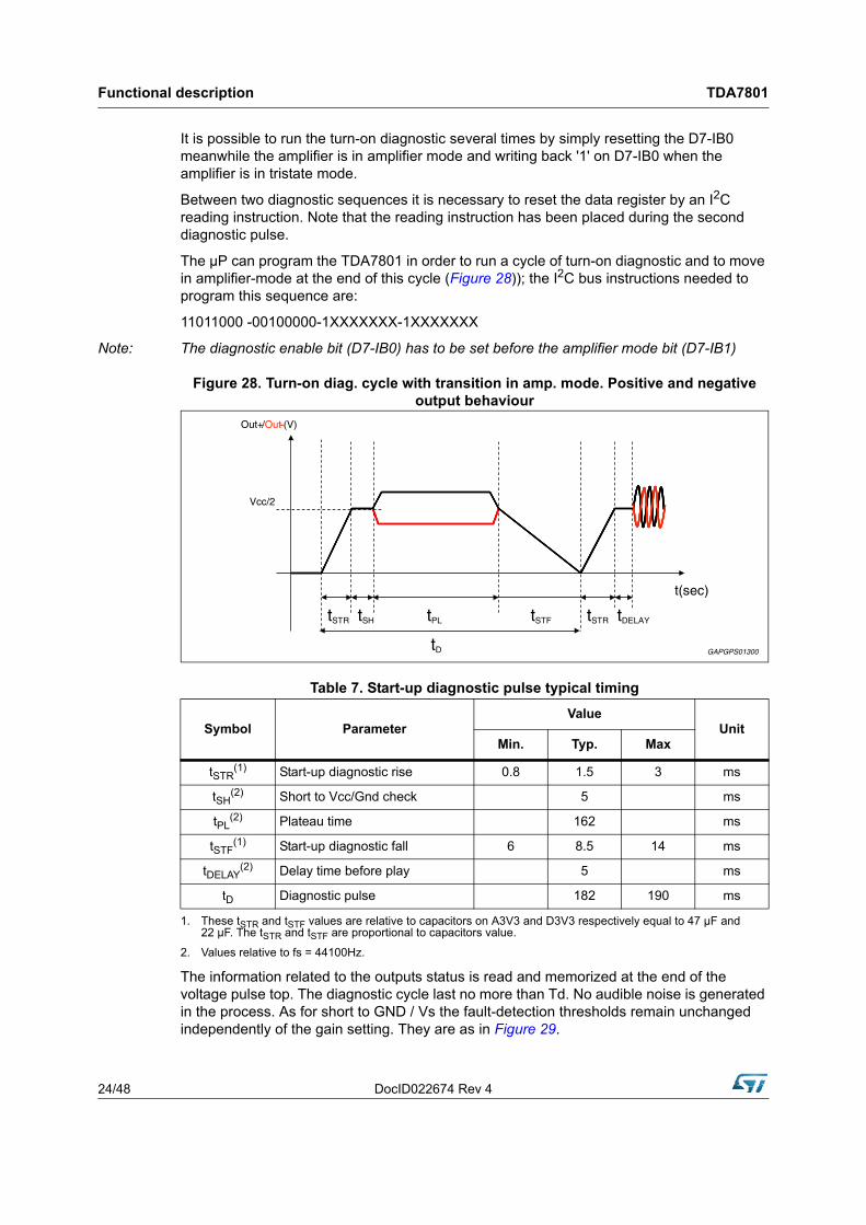
The µP can program the TDA7801 in order to run a cycle of turn-on diagnostic and to move in amplifier-mode at the end of this cycle (Figure 28)); the I2C bus instructions needed to program this sequence are:
11011000 -00100000-1XXXXXXX-1XXXXXXX
Note: The diagnostic enable bit (D7-IB0) has to be set before the amplifier mode bit (D7-IB1)
Figure 28. Turn-on diag. cycle with transition in amp. mode. Positive and negative output behaviour
The information related to the outputs status is read and memorized at the end of the voltage pulse top. The diagnostic cycle last no more than Td. No audible noise is generated in the process. As for short to GND / Vs the fault-detection thresholds remain unchanged independently of the gain setting. They are as in Figure 29.
Table 7. Start-up diagnostic pulse typical timing
Symbol ParameterValue
UnitMin. Typ. Max
tSTR(1)
1. These tSTR and tSTF values are relative to capacitors on A3V3 and D3V3 respectively equal to 47 µF and 22 µF. The tSTR and tSTF are proportional to capacitors value.
Start-up diagnostic rise 0.8 1.5 3 ms
tSH(2)
2. Values relative to fs = 44100Hz.
Short to Vcc/Gnd check 5 ms
tPL(2) Plateau time 162 ms
tSTF(1) Start-up diagnostic fall 6 8.5 14 ms
tDELAY(2) Delay time before play 5 ms
tD Diagnostic pulse 182 190 ms
DocID022674 Rev 4 25/48
TDA7801 Functional description
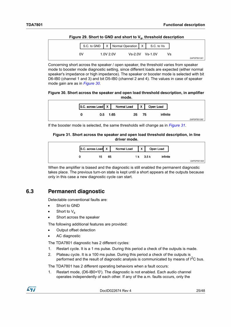
Figure 29. Short to GND and short to Vs, threshold description
Concerning short across the speaker / open speaker, the threshold varies from speaker mode to booster mode diagnostic setting, since different loads are expected (either normal speaker's impedance or high impedance). The speaker or booster mode is selected with bit D6-IB0 (channel 1 and 3) and bit D5-IB0 (channel 2 and 4). The values in case of speaker mode gain are as in Figure 30.
Figure 30. Short across the speaker and open load threshold description, in amplifier mode.
If the booster mode is selected, the same thresholds will change as in Figure 31.
Figure 31. Short across the speaker and open load threshold description, in line driver mode.
When the amplifier is biased and the diagnostic is still enabled the permanent diagnostic takes place. The previous turn-on state is kept until a short appears at the outputs because only in this case a new diagnostic cycle can start.
6.3 Permanent diagnosticDetectable conventional faults are:
Short to GND
Short to Vs
Short across the speaker
The following additional features are provided:
Output offset detection
AC diagnostic
The TDA7801 diagnostic has 2 different cycles:
1. Restart cycle. It is a 1 ms pulse. During this period a check of the outputs is made.
2. Plateau cycle. It is a 100 ms pulse. During this period a check of the outputs is performed and the result of diagnostic analysis is communicated by means of I2C bus.
The TDA7801 has 2 different operating behaviors when a fault occurs:
1. Restart mode, (D6-IB0='0'). The diagnostic is not enabled. Each audio channel operates independently of each other. If any of the a.m. faults occurs, only the

Functional description TDA7801
26/48 DocID022674 Rev 4
channel(s) concerned are shut down. The diagnostic performs restart cycles every 1 ms until a fault condition is present. The amplifier restarts in play only once the overload is removed.DIagnostic mode, (D6-IB0='1'). It is enabled via I2C bus and self activates if an output overload (so as to cause the intervention of the short-circuit protection) occurs to the speakers outputs. Once activated, the diagnostics procedure develops as below:
– The diagnostic performs 1 restart cycle in order to avoid momentary re-circulation spikes which could give erroneous diagnostic results. If normal situation (no overloads) is detected the channel returns active.
– Instead, if after 1 restart cycle an overload is detected then the diagnostic circuit performs a plateau cycle.
– After the plateau cycle, the fault audio channel generates restart cycles every 1 ms until a fault condition is present. The relevant data acquired during plateau cycle are stored and can be read by the microprocessor. A new plateau cycle can be activated by an I2C reading only if the fault condition persists. This is to ensure continuous diagnostics throughout the car-radio operating time.
The diagnostic performs another plateau cycle after each I2C bus registers read if the diagnostic bit is activated, (IB0-d7="1"). If I2C read is performed during the diagnostic permanent plateau cycle then, once the short is removed, the amplifier waits for another I2C read before starting to play again, in order to communicate the diagnostic plateau cycle results.
6.4 AC diagnostic
It is targeted at detecting accidental disconnection of tweeters in 2-way speaker and, more in general, presence of capacitive (AC) coupled loads. This diagnostic is based on the notion that the overall speaker's impedance (woofer + parallel tweeter) will tend to increase towards high frequencies if the tweeter gets disconnected, because the remaining speaker (woofer) would be out of its operating range (high impedance).To determine the load impedance, a sinewave tone at a suitable (F > 10 kHz or even ultrasonic) frequency should be fed to the output pins. Depending on the test's result the AC diagnostic is able to determine if the tweeter is connected or not. The tweeter is not connected if for four consecutive sine wave the current threshold on the load is not res-passed.AC diagnostic is managed by I2C commands. The AC diagnostic is enabled by bit D7 of register IB4, while the bit D6 is used to choose the current level threshold. The result of AC test are stored in the data register DB4 (bits D7:D4) which are set to logic level '1' if a tweeter is detected on the correspondent channel.
Note, the results on D7:D4 are valid only if the bit D3 is zero; in order to avoid this condition the pulse generated has to respect the condition Vout_peak < Vbattery-4V.
6.5 Output DC offset detection
Any DC output offset exceeding ± VO are signalled out. This inconvenient might occur as a consequence of improper DC input signal. The offset detection is performed at the end of the digital chain by a low pass digital filter. The offset detection is permanent, and also works in play mode. The results of the DC offset detection are obtained from the right pin for each channel (see I2C table in Section 9); the bits are continuously refreshed.

DocID022674 Rev 4 27/48
TDA7801 Functional description
6.6 Multiple faults
Faults can occur simultaneously. If this happens, faults are read out according to a "priority table" (see Table 8); this guarantees that the most dangerous fault is signalled. This is true only for the turn-on diagnostic but not in case of permanent diagnostic (only the faults causing protection intervention are recognized).
In permanent diagnostic mode the table is the same, with only a difference concerning open load, which is not among the recognizable faults. If an open load is present during the device's normal operation, it should be detected at a subsequent turn-on diagnostic cycle (i.e. at the successive car radio turn-on).
6.7 Faults availability
All the results coming from I2C bus, by read operations, are the consequence of measurements inside a defined period of time. If the fault is stable throughout the whole period, it will be sent out.
The turn-on diagnostic faults are reported on the byte DB 0-3 at the bits D 4-0. The faults are consistent when the bit D6 of DB0 is '1'. The byte DB 0-3 is reset when read.
During Amplifier-mode, when the bit D4 of byte DB 0-3 is '1' an overload on the correspondent channel has been detected and a 100 ms permanent diagnostic cycle has been done. The data on the bits D 4-0 reports the results of this diagnostic cycle. If the bits are all zero it means that an overload event has been detected, a 100ms cycle has been performed and the fault has not been detected or removed.
6.8 I2C programming/reading sequence
A correct turn on/off sequence respectful of the diagnostic timings and producing no audible noises could be as follows (after battery connection):
a) Turn-on: (Stand-by out + DIag Enable) 200 ms (min.) Muting out
b) Turn-off: Muting in 10 ms (Diag disable + stand-by in)
c) Car radio installation: DIag enable (write) 200 ms I2C read (repeat until all faults disappear).
Table 8. Multiple faults priority
S. GND S. Vs S. Across L. Open L.
S. GND S. GND S. Vs + S. GND S. GND S. GND
S. Vs / S. Vs S. Vs S. Vs
S. Across L. / / S. Across L. N.A.
Open L. / / / Open Load (1)
1. Only in Startup Diagnostic

Functional description TDA7801
28/48 DocID022674 Rev 4
6.9 Legacy mode
In case of applications without the I2C bus the TDA7801 could be turned on in legacy mode.
In order to put the device in legacy mode it is enough to tie the IC clock pin (PIN 27) at Vcc. In this mode the device is turned on, as usual, with the ENABLE pin (PIN 2). The I2C Data pin (PIN26) acts as analog mute. The device is set with all the instruction registers equal to zero.
In legacy mode the I2S interface does not support the TDM format.
6.10 Thermal protection
The TDA7801 has four thermal warnings (Tw1, Tw2, Tw3, Tw4) at different temperatures which are stored on the I2C bus. Only one of the four thermal warnings could be sent to the DIAG pin. The selection is done by an I2C bus.
A mute function dependent on temperature is present in order to protect the junction by over-temperature with limited effects on the sound quality. For junction temperature over the thermal warning threshold Tpl, the device is gradually carried in mute. The mute level depends on the temperature: when the junction temperature reaches the Tpl threshold (refer to Figure 32), the output signal is attenuated of 0.5 dB, while when the junction temperature reaches Tph the output attenuation is 60 dB. This attenuation is performed without output signal distortion.
Figure 32. Thermal muting diagram

DocID022674 Rev 4 29/48
TDA7801 Functional description
6.11 Under-voltage threshold
6.11.1 Supply voltage auto-mute threshold
The device in play-mode is put in mute when the supply voltage gets lower than the VAM threshold.
When the supply voltage gets lower than the VAM threshold the device is put in mute. The muting strategy in this case is reported in Figure 33: once the supply voltage Vs becomes lower than VAM_HIGH, analog mute and digital mute are activated. The analog mute attenuation is proportional to the Vs voltage and becomes equal to AM when the Vs gets lower than VAM_LOW. Note that once the digital mute procedure is started, it cannot be stopped to move back the device in play, the procedure is going on until the attenuation level has reached AM. This mechanism avoids that a fast oscillation on Vs cause a similar oscillation on the output.
Figure 33. Low voltage mute attenuation, supply voltage variation (Vs); result digital attenuation (At)
6.11.2 Digital mute disabling
The digital mute is disabled in the following conditions:
when TW1 threshold is trespassed (to avoid simultaneous intervention of digital mute and thermal mute)
when the bit IB3-D5 is set to '1'
during the start-up diagnostic
When the digital mute is disabled, the analog mute is kept active.
6.11.3 Power-on reset threshold
When the ENABLE pin is low or the supply voltage value doesn't guarantee the integrity of The I2C bus registers (VPOWERONRESET) the TDA7801 is put in tristate-mode and the registers are set to the initial state. The event is signalled by the low value of DIAG pin and the '0' value of bit D7 of byte DB0. The DIAG pin is set to high after a POR when the bit D7 of byte IB1 is set to '1' (amplifier mode on) if no other event on DIAG pin is present. The same I2C bus write operation automatically set to '1' the bit D7 of byte DB0. When the device is programmed with the D7=1 of IB0 and D7=1 of byte IB1 the device turns-on after a diagnostic cycle and the DIAG pin stays low for the whole duration of the diagnostic cycle.

Functional description TDA7801
30/48 DocID022674 Rev 4
6.12 Fast mute features
The TDA7801 is put in mute by a fast-mute procedure by one of the following event:
the ENABLE pin is set to low
the PLL loses the locking
the VS voltage level is under the auto-mute threshold.
by an I2C programming
DocID022674 Rev 4 31/48
TDA7801 I2S bus interface
7 I2S bus interface
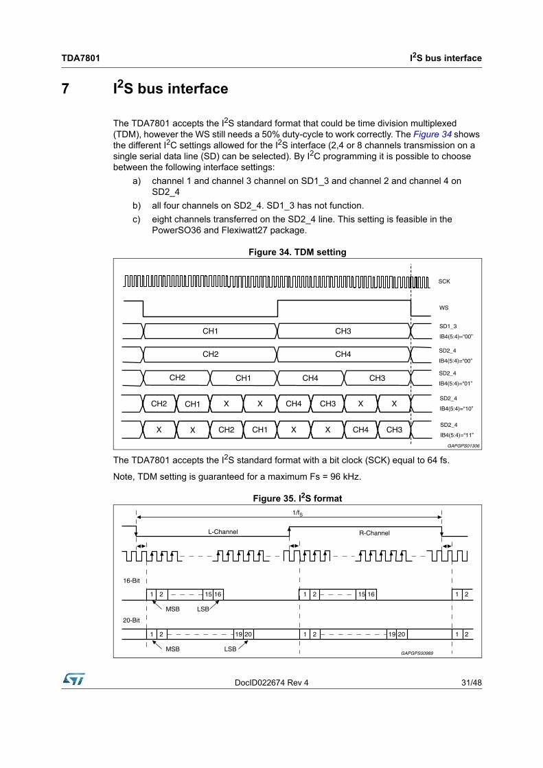
The TDA7801 accepts the I2S standard format that could be time division multiplexed (TDM), however the WS still needs a 50% duty-cycle to work correctly. The Figure 34 shows the different I2C settings allowed for the I2S interface (2,4 or 8 channels transmission on a single serial data line (SD) can be selected). By I2C programming it is possible to choose between the following interface settings:
a) channel 1 and channel 3 channel on SD1_3 and channel 2 and channel 4 on SD2_4
b) all four channels on SD2_4. SD1_3 has not function.
c) eight channels transferred on the SD2_4 line. This setting is feasible in the PowerSO36 and Flexiwatt27 package.
Figure 34. TDM setting
The TDA7801 accepts the I2S standard format with a bit clock (SCK) equal to 64 fs.
Note, TDM setting is guaranteed for a maximum Fs = 96 kHz.
Figure 35. I2S format
I2S bus interface TDA7801
32/48 DocID022674 Rev 4
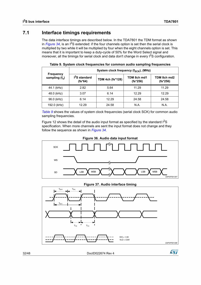
7.1 Interface timings requirements
The data interface timings are described below. In the TDA7801 the TDM format as shown in Figure 34, is an I2S extended: if the four channels option is set then the serial clock is multiplied by two while it will be multiplied by four when the eight channels option is set. This means that it is important to keep a duty-cycle of 50% for the Word Select signal and moreover, all the timings for serial clock and data don't change in every I2S configuration.
Table 9 shows the values of system clock frequencies (serial clock SCK) for common audio sampling frequencies.
Figure 12 shows the detail of the audio input format as specified by the standard I2S specification. When more channels are sent the input format does not change and they follow the sequence as shown in Figure 34.
Figure 36. Audio data input format
Figure 37. Audio interface timing
Table 9. System clock frequencies for common audio sampling frequencies
Frequency sampling (fs)
System clock frequency (fSCK), (MHz)
I2S standard (fs*64)
TDM 4ch (fs*128)TDM 8ch md1
(fs*256)TDM 8ch md2
(fs*256)
44.1 (kHz) 2.82 5.64 11.29 11.29
48.0 (kHz) 3.07 6.14 12.29 12.29
96.0 (kHz) 6.14 12.29 24.58 24.58
192.0 (kHz) 12.29 24.58 N.A. N.A.

DocID022674 Rev 4 33/48
TDA7801 I2S bus interface
7.2 Group delay
The group delay of the amplifier is basically due the FIR filter of the interpolator and it is given by:
, (fs < 48 kHz)
Table 10. Example timing for tck = 1/fSCK, where fSCK is stated in the Table 9
Parameter MIN TYP MAX Note
Clock period TSKY 0.9*Tck Tck 1.1*Tck
Clock HIGH TSKH 0.4*TckMeasured from VHI to VHI
Clock LOW TSKL 0.4*TckMeasured from VLO to VLO
Setup time SD to fSCK rising edge TDS 0.2*Tck
Hold time SD from fSCK rising edge THD 0.2*Tck 0.8*Tck (1)
1. Measured from VLO to VHI.
fSCK duty-cycle 40% 60%
VHI 1.3
VLO 0.8
tDELAY32fs------=

I2C bus interface TDA7801
34/48 DocID022674 Rev 4
8 I2C bus interface
Data transmission from microprocessor to the TDA7801 and viceversa takes place through the 2 wires I2C bus interface, consisting of the two lines SDA and SCL (pull-up resistors to positive supply voltage must be connected).
When I2C bus is active any operating mode of the IC may be modified and the diagnostic may be controlled and results read back.
The protocol used for the bus is depicted in Figure 38 and comprises:
a start condition (S)
a chip address byte (the LSB bit determines read/write transmission)
a subaddress byte
a sequence of data (N-bytes + acknowledge)
a stop condition (P)
Figure 38. I2C bus protocol description
Description:
S = Start
R/W = '0' => Receive-Mode (Chip could be programmed by µP)
I = Auto increment; when 1, the address is automatically increased for each byte transferred
X: not used
A = Acknowledge
P = Stop
MAX CLOCK SPEED 400kbit/sec
* = available in PowerSO36

DocID022674 Rev 4 35/48
TDA7801 I2C bus interface
8.1 Writing procedure
There are two possible procedures:
1. without increment: the I bit is set to 0 and the register is addressed by the subaddress. Only this register is written by the data following the subaddress byte.
2. with increment: the I bit is set to 1 and the first register written is the one addressed by subaddress. Then all the registers starting from the one indicated by this address up to stop bit (or up to last register) are written.
8.2 Reading procedure
There are two possible procedures:
1. without increment: the I bit is set to 0 and the register is addressed by the subaddress sent in the previous write procedure. Only this register is read by the data following the address.
2. with increment: the I bit is set to 1 and the first register read is the one addressed by subaddress sent in the previous write procedure. Then all registers starting from the one indicated by this address up to stop bit (or up to last register) are read.
Note: the reading procedure reset the register that has been read.
8.3 Data validity
The data on the SDA line must be stable during the high period of the clock. The high and low state of the data line can only change when the clock signal on the SCL line is low.
8.4 Start and stop conditions
A start condition is a high to low transition of the SDA line while SCL is high.The stop condition is a low to high transition of the SDA line while SCL is high.
8.5 Byte format
Every byte transferred to the SDA line must contain 8 bits. Each byte must be followed by an acknowledge bit. The MSB is transferred first.
8.6 Acknowledge
The transmitter* puts a resistive HIGH level on the SDA line during the acknowledge clock pulse. The receiver** has to pull-down the SDA line during the acknowledge clock pulse, so that the SDA line is stable low using this clock pulse.
* Transmitter
= master (µP) when it writes an address to the TDA7801= slave (TDA7801) when the µP reads a data byte from TDA7801
** Receiver
= slave (TDA7801) when the µP writes an address to the TDA7801= master (µP) when it reads a data byte from TDA7801

I2C registers TDA7801
36/48 DocID022674 Rev 4
9 I2C registers
9.1 IB0-Addr:"00000"
9.2 IB1-Addr:"00001"
Table 11. IB0-Addr:"00000"
Bit Instruction decoding bit
D70: diagnostic defeat 1: diagnostic enable
D60: Speaker mode diagnostic ch. 1 and 3 (FRONT)1: Booster mode diagnostic ch. 1 and 3
D50: Speaker mode diagnostic ch. 2 and 4 (REAR)1: Booster mode diagnostic ch. 2 and 4
D4 Gain channel 1 and 3 (FRONT)D4 D300 GV101 GV210 GV311 GV4
D3
D2 Gain channel 2 and 4 (REAR)D2 D100 GV101 GV210 GV311 GV4
D1
D00: No increase of digital gain1: +6dB increase of digital gain
Table 12. IB1-Addr:"00001"
Bit Instruction decoding bit
D70: Amplifier mode off - Amplifier not working1: Amplifier mode on - Amplifier working
D6 Mute Time SettingD6 D5 D4 mute timing(Fs=44.1kHz)
000 1.45 ms001 5.8 ms010 11.6 ms011 23.2 ms100 34.8 ms101 69.6 ms110 140 ms111 278 ms
D5
D4
D30: Mute channel 1 and 3 (FRONT)1: Unmute channel 1 and 3

DocID022674 Rev 4 37/48
TDA7801 I2C registers
9.3 IB2-Addr:"00010"
D20: Mute channel 2 and 4 (REAR)1: Unmute channel 2 and 4
D1 Sample Frequency Range(1)
D1 D0 00 44.1/48 kHz01 44.1/48 kHz10 96 kHz11 192 kHz
D0
1. When the amplifier is in Tristate Mode (IB0-D7=0 and IB1-D7=0), any accidental change of Frequency sample is ignored.
Table 12. IB1-Addr:"00001" (continued)
Bit Instruction decoding bit
Table 13. IB3-Addr:"00010"
Bit Instruction decoding bit
D70: no short fault information on diag. pin1: short fault information on diag. pin
D60: Offset information on diag pin1: no offset information on diag pin
D5 Temperature warning information on diag. pinD5 D4 D3000 Tw1001 Tw2010 Tw3011 Tw41xx no thermal warning information on diag. pin
D4
D3
D2 Clip detection levelD2 D100 1 %01 5 %10 10 %11 clip detection disabled
D1
D0 0 (no selectable from user)

I2C registers TDA7801
38/48 DocID022674 Rev 4
9.4 IB3-Addr:"00011"
9.5 IB4-Addr:"00100"
Table 14. IB3-Addr:"00011"
Bit Instruction decoding bit
D70: Noise gating on1: Noise gating off
D6 0 (not used)
D50: under-voltage digital mute on
1: under-voltage digital mute off
D4Tristate channel 3 (right front)0: ch.3 not in tristate1: ch.3 in tristate
D3Tristate channel 1 (left front)0: ch.1 not in tristate1: ch.1 in tristate
D2Tristate channel 4 (right rear)0: ch.4 not in tristate1: ch.4 in tristate
D1Tristate channel 2 (left rear)0: ch.2 not in tristate1: ch.2 in tristate
D00: Input high pass filter off1: Input high pass filter on
Table 15. IB4-Addr:"00100"
Bit Instruction decoding bit
D7 AC diagnostic On (D7='1')
D6AC diagnostic current thresholdD6 = '0': highD6 = '1': low
D5 TDM
00 I2S standard
01 I2S - 4 ch
10 I2S - 8 ch (first channels)
11 I2S - 8 ch (last channels)
D4
D3 0 (not used)
D2 0 (not used)
D1 0 (not used)
D0 0 (not used)
DocID022674 Rev 4 39/48
TDA7801 I2C registers
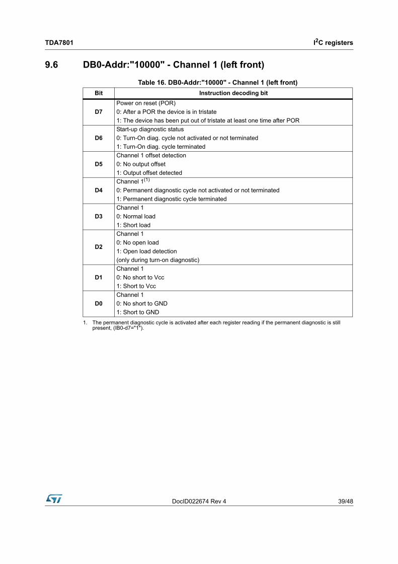
9.6 DB0-Addr:"10000" - Channel 1 (left front)
Table 16. DB0-Addr:"10000" - Channel 1 (left front)
Bit Instruction decoding bit
D7
Power on reset (POR)
0: After a POR the device is in tristate
1: The device has been put out of tristate at least one time after POR
D6
Start-up diagnostic status
0: Turn-On diag. cycle not activated or not terminated
1: Turn-On diag. cycle terminated
D5
Channel 1 offset detection
0: No output offset
1: Output offset detected
D4
Channel 1(1)
0: Permanent diagnostic cycle not activated or not terminated
1: Permanent diagnostic cycle terminated
1. The permanent diagnostic cycle is activated after each register reading if the permanent diagnostic is still present, (IB0-d7="1").
D3
Channel 1
0: Normal load
1: Short load
D2
Channel 1
0: No open load
1: Open load detection
(only during turn-on diagnostic)
D1
Channel 1
0: No short to Vcc
1: Short to Vcc
D0
Channel 1
0: No short to GND
1: Short to GND

I2C registers TDA7801
40/48 DocID022674 Rev 4
9.7 DB1-Addr:"10001" - Channel 2 (left rear)
Table 17. DB1-Addr:"10001" - Channel 2 (left rear)
Bit Instruction decoding bit
D7
TW1 active
0: TW1 threshold not trespassed
1: TW1 threshold tress-passed
D6
TW2 active
0: TW2 threshold not trespassed
1: TW2 threshold tress-passed
D5
Channel 2 offset detection
0: No output offset
1: Output offset detected
D4
Channel 2(1)
0: permanent diag. cycle not activated or not terminated
1: Permanent diag. cycle terminated
1. The permanent diagnostic cycle is activated after each register reading if the permanent diagnostic is still present.
D3
Channel 2
0: Normal load
1: Short load
D2
Channel 2
0: No open load
1: Open load detection
(only during turn-on diagnostic)
D1
Channel 2
0: No short to Vcc
1: Short to Vcc
D0
Channel 2
0: No short to GND
1: Short to GND
DocID022674 Rev 4 41/48
TDA7801 I2C registers
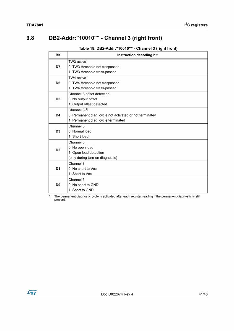
9.8 DB2-Addr:"10010"" - Channel 3 (right front)
Table 18. DB2-Addr:"10010"" - Channel 3 (right front)
Bit Instruction decoding bit
D7
TW3 active
0: TW3 threshold not trespassed
1: TW3 threshold tress-passed
D6
TW4 active
0: TW4 threshold not trespassed
1: TW4 threshold tress-passed
D5
Channel 3 offset detection
0: No output offset
1: Output offset detected
D4
Channel 3(1)
0: Permanent diag. cycle not activated or not terminated
1: Permanent diag. cycle terminated
1. The permanent diagnostic cycle is activated after each register reading if the permanent diagnostic is still present.
D3
Channel 3
0: Normal load
1: Short load
D2
Channel 3
0: No open load
1: Open load detection
(only during turn-on diagnostic)
D1
Channel 3
0: No short to Vcc
1: Short to Vcc
D0
Channel 3
0: No short to GND
1: Short to GND

I2C registers TDA7801
42/48 DocID022674 Rev 4
9.9 DB3-Addr:"10011" - Channel 4 (right rear)
9.10 DB4-Addr:"10100"
Table 19. DB3-Addr:"10011" - Channel 4 (right rear)
Bit Instruction decoding bit
D70: channel 2 and 4 in play (FRONT)
1: channel 2 and 4 in mute
D60: channel 1 and 3 in play (REAR)
1: channel 1 and 3 in mute
D5
Channel 4 offset detection
0: No output offset
1: Output offset detected
D4
Channel 4(1)
0: permanent diag. cycle not activated or not terminated
1: Permanent diag. cycle terminated
1. The permanent diagnostic cycle is activated after each register reading if the permanent diagnostic is still present.
D3
Channel 4
0: Normal load
1: Short load
D2
Channel 4
0: No open load
1: Open load detection
(only during turn-on diagnostic)
D1
Channel 4
0: No short to Vcc
1: Short to Vcc
D0
Channel 4
0: No short to GND
1: Short to GND
Table 20. DB4-Addr:"10100"
Bit Instruction decoding bit
D7 Ch1 tweeter present
D6 Ch2 tweeter present
D5 Ch3 tweeter present
D4 Ch4 tweeter present
D3 Signal to high
D2 0
D1 0
D0 0
DocID022674 Rev 4 43/48
TDA7801 Package information
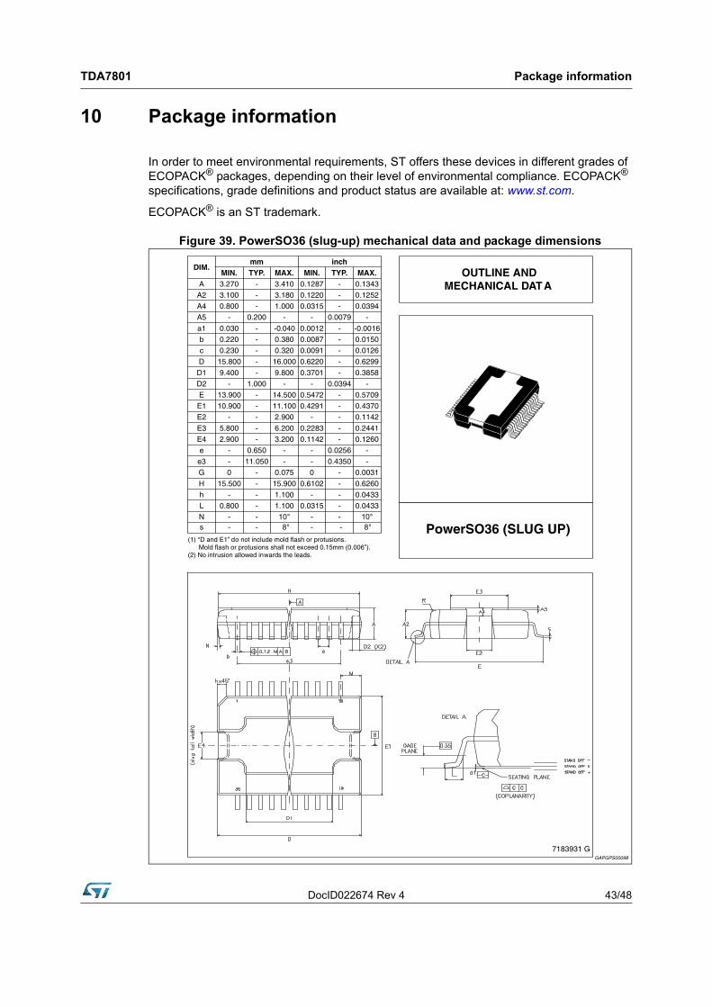
10 Package information
In order to meet environmental requirements, ST offers these devices in different grades of ECOPACK® packages, depending on their level of environmental compliance. ECOPACK® specifications, grade definitions and product status are available at: www.st.com.
ECOPACK® is an ST trademark.
Figure 39. PowerSO36 (slug-up) mechanical data and package dimensions

Package information TDA7801
44/48 DocID022674 Rev 4
Figure 40. Flexiwatt27 (vertical) mechanical data and package dimensions

DocID022674 Rev 4 45/48
TDA7801 Package information
Figure 41. Flexiwatt27 (horizontal) mechanical data and package dimensions

Package information TDA7801
46/48 DocID022674 Rev 4
Figure 42. Flexiwatt27 (SMD) mechanical data and package dimensions
DocID022674 Rev 4 47/48
TDA7801 Revision history
11 Revision history
Table 21. Document revision history
Date Revision Changes
13-Feb-2012 1 Initial release.
11-Dec-2012 2Corrected typeset error of the "a1" dimension on the Figure 39: PowerSO36 (slug-up) mechanical data and package dimensions on page 43.
26-Feb-2013 3 Updated Table 4: Absolute maximum ratings on page 12.
18-Sep-2013 4 Updated Disclaimer.

TDA7801
48/48 DocID022674 Rev 4
Please Read Carefully:
Information in this document is provided solely in connection with ST products. STMicroelectronics NV and its subsidiaries (“ST”) reserve theright to make changes, corrections, modifications or improvements, to this document, and the products and services described herein at anytime, without notice.
All ST products are sold pursuant to ST’s terms and conditions of sale.
Purchasers are solely responsible for the choice, selection and use of the ST products and services described herein, and ST assumes noliability whatsoever relating to the choice, selection or use of the ST products and services described herein.
No license, express or implied, by estoppel or otherwise, to any intellectual property rights is granted under this document. If any part of thisdocument refers to any third party products or services it shall not be deemed a license grant by ST for the use of such third party productsor services, or any intellectual property contained therein or considered as a warranty covering the use in any manner whatsoever of suchthird party products or services or any intellectual property contained therein.
UNLESS OTHERWISE SET FORTH IN ST’S TERMS AND CONDITIONS OF SALE ST DISCLAIMS ANY EXPRESS OR IMPLIED WARRANTY WITH RESPECT TO THE USE AND/OR SALE OF ST PRODUCTS INCLUDING WITHOUT LIMITATION IMPLIED WARRANTIES OF MERCHANTABILITY, FITNESS FOR A PARTICULAR PURPOSE (AND THEIR EQUIVALENTS UNDER THE LAWS OF ANY JURISDICTION), OR INFRINGEMENT OF ANY PATENT, COPYRIGHT OR OTHER INTELLECTUAL PROPERTY RIGHT.
ST PRODUCTS ARE NOT DESIGNED OR AUTHORIZED FOR USE IN: (A) SAFETY CRITICAL APPLICATIONS SUCH AS LIFE SUPPORTING, ACTIVE IMPLANTED DEVICES OR SYSTEMS WITH PRODUCT FUNCTIONAL SAFETY REQUIREMENTS; (B) AERONAUTIC APPLICATIONS; (C) AUTOMOTIVE APPLICATIONS OR ENVIRONMENTS, AND/OR (D) AEROSPACE APPLICATIONS OR ENVIRONMENTS. WHERE ST PRODUCTS ARE NOT DESIGNED FOR SUCH USE, THE PURCHASER SHALL USE PRODUCTS AT PURCHASER’S SOLE RISK, EVEN IF ST HAS BEEN INFORMED IN WRITING OF SUCH USAGE, UNLESS A PRODUCT IS EXPRESSLY DESIGNATED BY ST AS BEING INTENDED FOR “AUTOMOTIVE, AUTOMOTIVE SAFETY OR MEDICAL” INDUSTRY DOMAINS ACCORDING TO ST PRODUCT DESIGN SPECIFICATIONS. PRODUCTS FORMALLY ESCC, QML OR JAN QUALIFIED ARE DEEMED SUITABLE FOR USE IN AEROSPACE BY THE CORRESPONDING GOVERNMENTAL AGENCY.
Resale of ST products with provisions different from the statements and/or technical features set forth in this document shall immediately voidany warranty granted by ST for the ST product or service described herein and shall not create or extend in any manner whatsoever, anyliability of ST.
ST and the ST logo are trademarks or registered trademarks of ST in various countries.Information in this document supersedes and replaces all information previously supplied.
The ST logo is a registered trademark of STMicroelectronics. All other names are the property of their respective owners.
© 2013 STMicroelectronics - All rights reserved
STMicroelectronics group of companies
Australia - Belgium - Brazil - Canada - China - Czech Republic - Finland - France - Germany - Hong Kong - India - Israel - Italy - Japan - Malaysia - Malta - Morocco - Philippines - Singapore - Spain - Sweden - Switzerland - United Kingdom - United States of America
www.st.com


![dU=TdS-pdV · 2020. 12. 10. · P(v2)d3v = (m 2πkT)3/2exp[− mv2 2 kT]d3v 速度が にある確率分布はマクスウェル 分布; [v,v+dv] で与えられる。 mv2 2 が自由粒子のエネルギー](https://img.dokumen.tips/doc/110x75/60b21c938f4e11367a6658c5/dutds-pdv-2020-12-10-pv2d3v-m-2kt32expa-mv2-2-ktd3v-eoe.jpg)