Embed Size (px)
Citation preview

Digital Design LaboaratoryDr. Oniga István
University of Debrecen, Faculty of Informatics

ISE tutorial
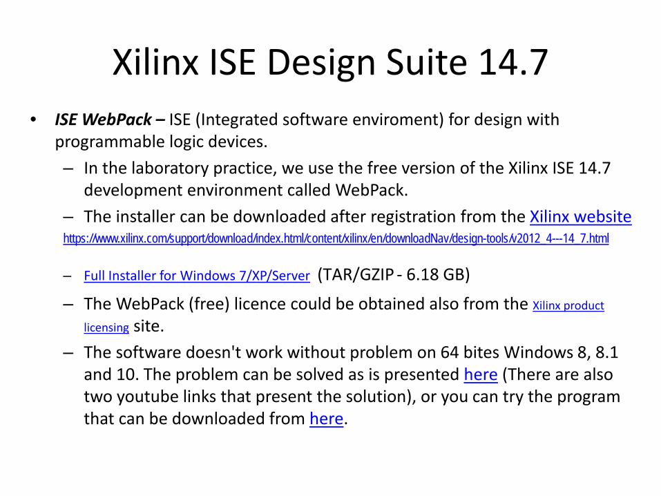
Xilinx ISE Design Suite 14.7• ISE WebPack – ISE (Integrated software enviroment) for design with
programmable logic devices. – In the laboratory practice, we use the free version of the Xilinx ISE 14.7
development environment called WebPack. – The installer can be downloaded after registration from the Xilinx websitehttps://www.xilinx.com/support/download/index.html/content/xilinx/en/downloadNav/design-tools/v2012_4---14_7.html
– Full Installer for Windows 7/XP/Server (TAR/GZIP - 6.18 GB)
– The WebPack (free) licence could be obtained also from the Xilinx product
licensing site. – The software doesn't work without problem on 64 bites Windows 8, 8.1
and 10. The problem can be solved as is presented here (There are also two youtube links that present the solution), or you can try the program that can be downloaded from here.

Software enviroments• Design entry:
– Xilinx Foundation ISE– Alternatives
• Mentor Graphics: FPGA Advantage• Celoxica: DK Design Suite
• Design Synthesis:– XST: Xilinx Synthesis Technology– Mentor: Leonardo Spectrum– Synplicity: Synplify Pro– Celoxica: DK Design Suite
• Simulation:– Mentor: Modelsim– Aldec: Active-HDL– Celoxica: DK Design Suite
• In Circuit verification– Xilinx: ChipScope

ISE Design flow• Project Navigator
– Design entry + constraints)– RTL simulation- ( Testbench ) – Sinthesys– Implementation: TRANSLATE →MAP →PAR (place &
route)– Static timing analisys: (max clock frequency, propagation
delays etc.)– Bitstream generate and download (configuration file - .bit)
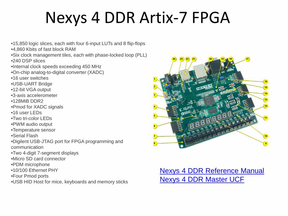
Nexys 4 DDR Artix-7 FPGA
Nexys 4 DDR Reference ManualNexys 4 DDR Master UCF
•15,850 logic slices, each with four 6-input LUTs and 8 flip-flops•4,860 Kbits of fast block RAM•Six clock management tiles, each with phase-locked loop (PLL)•240 DSP slices•Internal clock speeds exceeding 450 MHz•On-chip analog-to-digital converter (XADC)•16 user switches•USB-UART Bridge•12-bit VGA output•3-axis accelerometer•128MiB DDR2•Pmod for XADC signals•16 user LEDs•Two tri-color LEDs•PWM audio output•Temperature sensor•Serial Flash•Digilent USB-JTAG port for FPGA programming and communication•Two 4-digit 7-segment displays•Micro SD card connector•PDM microphone•10/100 Ethernet PHY•Four Pmod ports•USB HID Host for mice, keyboards and memory sticks

Digilent Nexys 2 • Xilinx Spartan-3E FPGA, 500K or 1200K gate• USB2 port providing board power, device configuration, and high-speed data transfers• Works with ISE/Webpack and EDK•16MB fast Micron PSDRAM•16MB Intel StrataFlash Flash R• Xilinx Platform Flash ROM• High-efficiency switching power supplies (good for battery-powered applications• 50MHz oscillator, plus a socket for a second oscillator• 75 FPGA I/O’s routed to expansion connectors (one high-speed Hirose FX2 connector with 43 signals and four 2x6 Pmod connectors)• All I/O signals are ESD and short-circuit protected, ensuring a long operating life in any environment.• On-board I/O includes eight LEDs, four-digit seven-segment display, four pushbuttons, eight slide switches• Ships in a DVD case with a high-speed USB2 cable• Requires Adept 2.0 or later for operation
Nexys 2 reference manual https://reference.digilentinc.com/reference/programmable-logic/nexys-2/reference-manualDigilent Nexys 2 kártya https://store.digilentinc.com/nexys-2-spartan-3e-fpga-trainer-board-retired-see-nexys-4-ddr/

Digilent Adept suite • Digilent Adept is a unique and powerful solution which allows you to communicate with Digilent system boards and a wide assortment of logic devices.
ADEPT for Windows
Adept 2 provide JTAG configuration and data transfering •Also adds board verification and I/O expansion features.
• Configure the Xilinx logic devices. Initialize a scan chain, program FPGAs, CPLDs, and PROMs, organize and keep track of your configuration files• Transfer data to and from the onboard FPGA on your system board. Read from and write to specified registers. Load a stream of data to a register or read a stream of data from a register.• Organize and quickly connect to your communications modules.• Program Xilinx XCFS Platform Flash devices using .bit or .mcs files.• Program Xilinx CoolRunner2 CPLDs using .jed files.• Program most Spartan and Virtex series FPGAs with .bit files
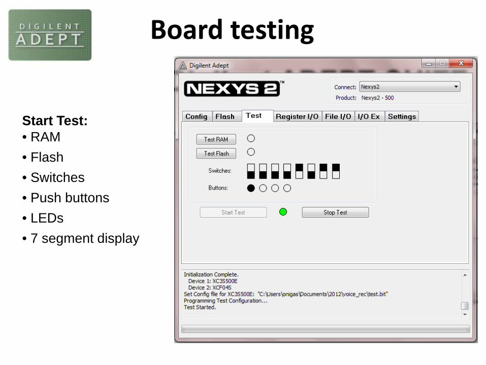
Board testing
Start Test:• RAM• Flash• Switches• Push buttons• LEDs• 7 segment display

Xilinx ISE
Sources window Editor
Console
Process window

Lab1_1 assignment
2 variable logic function implementation- schematic design -

Project creation• Start -> Programs\Xilinx ISE Design Suite 14.7\ISE Design Tools\Project Navigator. • File→New Project, • Name „first_sch” ,
– For the folder and the file name don’t use white-spaces.– The name could not start with numbers, but could contain numbers– For easier readability of error messages use different names for folders and files
• Top level source type: schematic!

Project settings• Next -> Device Properties -> Value :
• Next, Finish .
NEXYS 2 boardDevice Family: Spartan3EDevice: xc3s500EPackage: FG320Speed Grade: -4Synthesis Tool: XST (VHDL/Verilog)Simulator: ISim (VHDL/Verilog)Preffered Language: Verilog
NEXYS 4 DDR boardFamily: Artix7Device: XC7A100TPackage: CSG324Speed Grade: -3Synthesis Tool: XST (VHDL/Verilog)Simulator: ISim (VHDL/Verilog)Preffered Language: Verilog
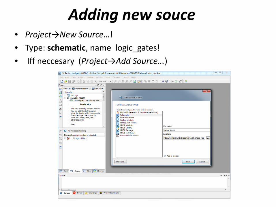
Adding new souce• Project→New Source…! • Type: schematic, name logic_gates!• Iff neccesary (Project→Add Source...)

Schematic project
Schematic design window

Task• Logic gates implementation

Tools for schematic design- Add wire- Add net name- Rename selected bus- Add bus tap- Add I/O marker- Add symbol
- Select components from the Symbols tab of the upper left pane and drag them to your schematic.
- You can narrow down your choices using the Categories, or by typing the first few characters of the symbol you’re looking for in the Symbol Name Filter, or just scroll through the lists. The important category for now is Logic: General logic gates.
- Use the wiring tool to wire up the components. It is in the tool bar and looks like a red line and a pencil.
- Place I/O Markers to the inputs and outputs using the I/O Marker widget.

Tools for schematic designChange the name of the marker to what you se on the assignment. You should double click the marker. Then click on “Nets” and then edit the “Name”, also observe the Port Polarity, then click OK.

Constraints file
• Project / New Source - > Implementation Constraint File-, name first.ucf• Next/Finish
https://blog.digilentinc.com/the-constraints-file-also-known-as-magical-moving-stairs/
• Specify what physical pins on the FPGA will be connected to I/O ports from the design (I/O markers)
NEXYS 2 boardNET “sw0" LOC = “B18" ; NET “sw1" LOC = “D18" ; NET "led0" LOC = “J14" ; NET "led1" LOC = “J15" ; NET "led2" LOC = “K15" ; NET "led3" LOC = “K14" ; NET "led4" LOC = “E17" ; NET "led5" LOC = “p15" ; NET "led6" LOC = “F4" ;
NEXYS 4DDR boardNET “sw0" LOC=J15 | IOSTANDARD=LVCMOS33; NET “sw1" LOC=L16 | IOSTANDARD=LVCMOS33; # LEDsNET "led0" LOC=H17 | IOSTANDARD=LVCMOS33;NET "led1" LOC=K15 | IOSTANDARD=LVCMOS33;NET "led2" LOC=J13 | IOSTANDARD=LVCMOS33; NET "led3" LOC=N14 | IOSTANDARD=LVCMOS33;NET "led4" LOC=R18 | IOSTANDARD=LVCMOS33; NET "led5" LOC=V17 | IOSTANDARD=LVCMOS33; NET "led6" LOC=U17 | IOSTANDARD=LVCMOS33;

Project implementation• Implement Design,
– View →implementation– Hierarchy window→ select top level file– Processes ablak → Implement Design
• Bit file generation

Configuration
• Final step in order to program the board. We will use the .bit file generated in the previous step.1. Using Impact program (part of ISE)2. Using Digilent Adept Suite https://www.digilentinc.com/Products/Detail.cfm?NavPath=2,66,828&Prod=ADEPT2
FPGA configuration:generated .bit (file)
1 2
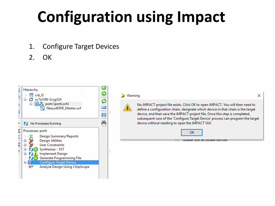
Configuration using Impact
1. Configure Target Devices2. OK
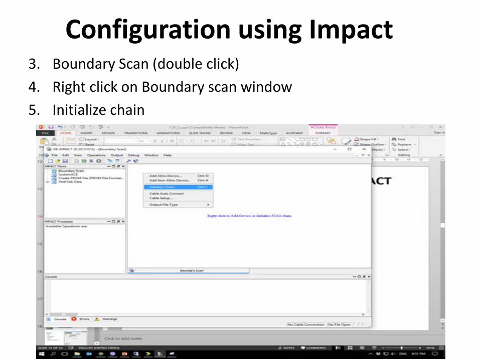
Configuration using Impact3. Boundary Scan (double click) 4. Right click on Boundary scan window5. Initialize chain

Configuration using Impact6. Assign new configuration file7. Open, No, Ok8. Right click on green icon, Program

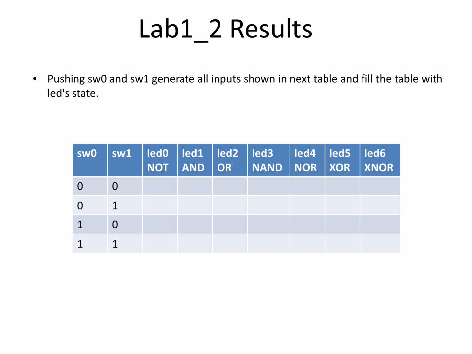
• Pushing sw0 and sw1 generate all inputs shown in next table and fill the table with led's state.
sw0 sw1 led0NOT
led1AND
led2OR
led3NAND
led4NOR
led5XOR
led6XNOR
0 0
0 1
1 0
1 1
Lab1_1Results

Lab1_2 assignment:
2 variable logic function implementation- HDL design entry -

New task• Logic gates implementation using Verilog
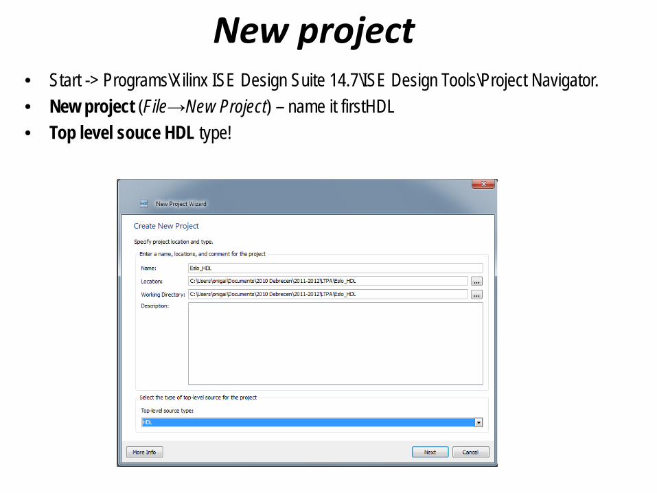
New project• Start -> Programs\Xilinx ISE Design Suite 14.7\ISE Design Tools\Project Navigator. • New project (File→New Project) – name it firstHDL• Top level souce HDL type!

Project settings• Next -> Device Properties -> Value :
NEXYS 2 boardDevice Family: Spartan3EDevice: xc3s500EPackage: FG320Speed Grade: -4Synthesis Tool: XST (VHDL/Verilog)Simulator: ISim (VHDL/Verilog)Preffered Language: Verilog
NEXYS 4 DDR boardFamily: Artix7Device: XC7A100TPackage: CSG324Speed Grade: -3Synthesis Tool: XST (VHDL/Verilog)Simulator: ISim (VHDL/Verilog)Preffered Language: Verilog
• Next, Finish.

Adding source file(HDL)• Project→New Source..! • Type Verilog Module, name firstHDL!• If necessary (Project→Add Source...)
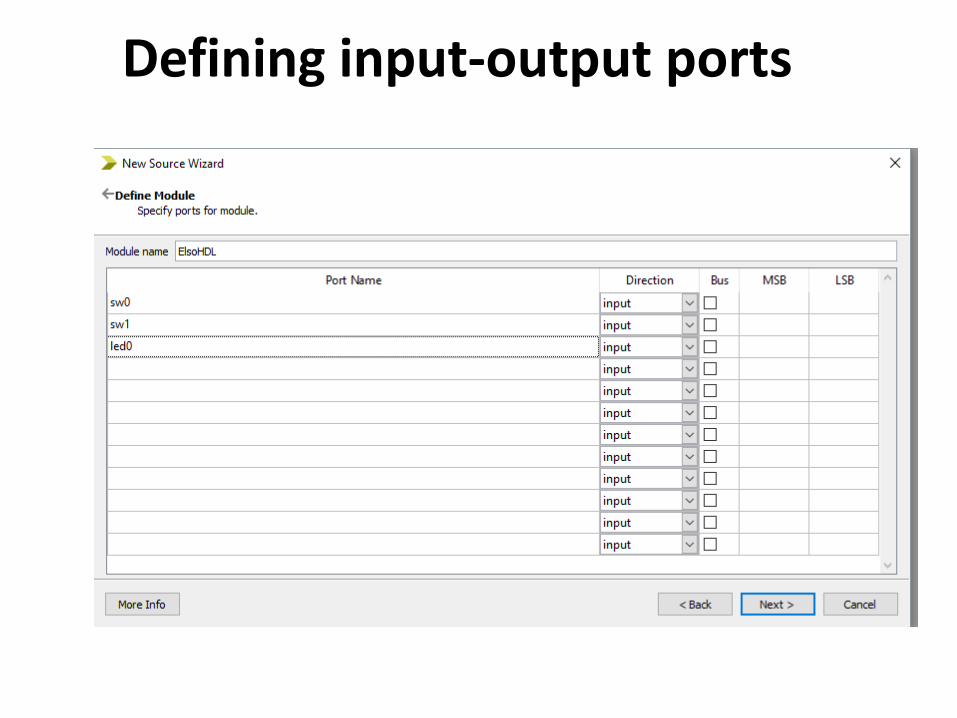
Defining input-output ports
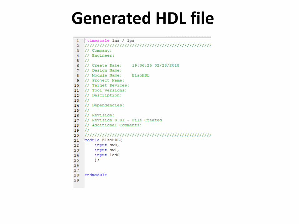
Generated HDL file
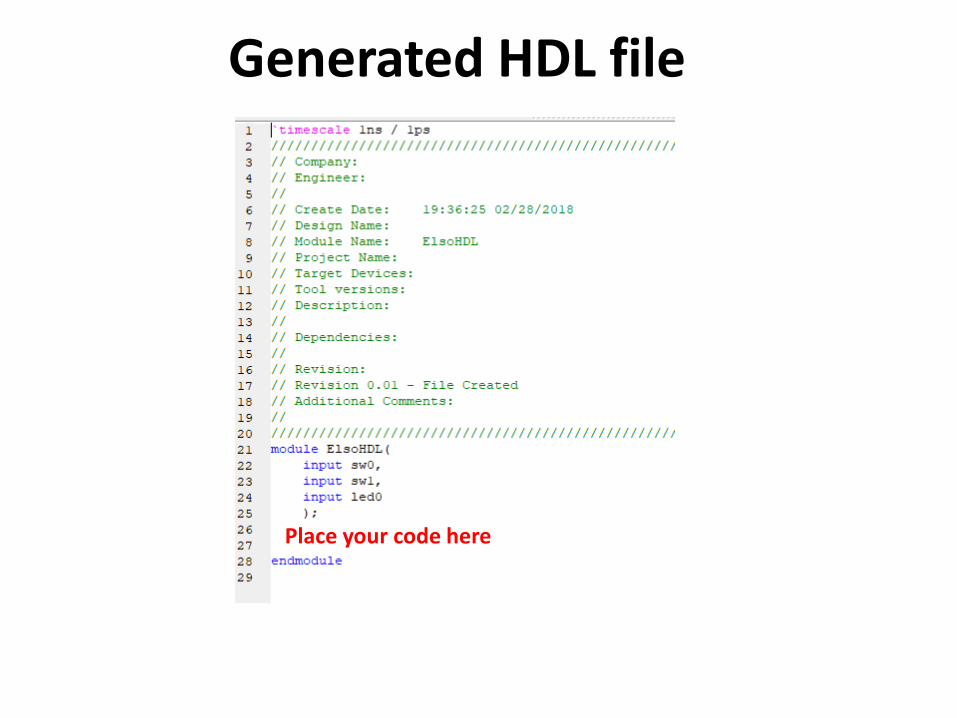
Generated HDL file
Place your code here

Constraint• Choose Project / Add Copy of Source first.ucf (created in last
project).• Press OK Sources window will show first.ucf file.
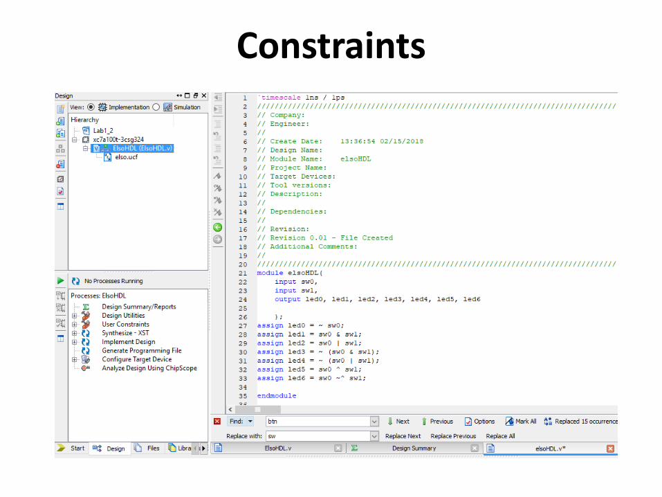
Constraints
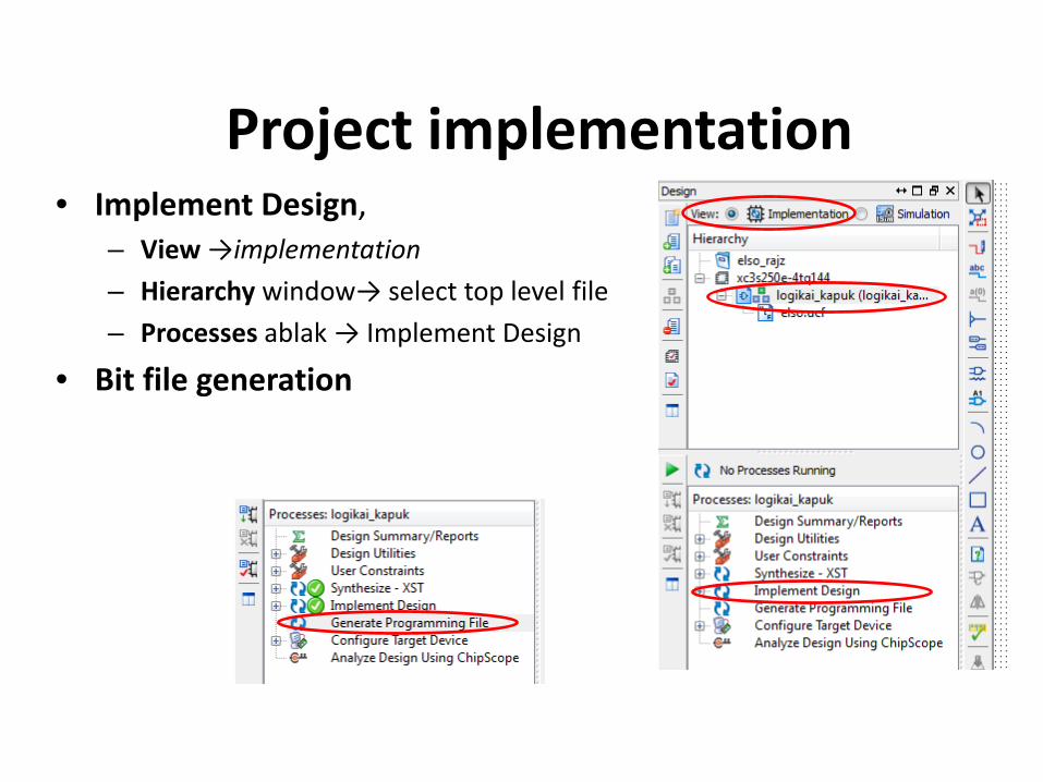
Project implementation• Implement Design,
– View →implementation– Hierarchy window→ select top level file– Processes ablak → Implement Design
• Bit file generation
Lab1_2 Results
sw0 sw1 led0NOT
led1AND
led2OR
led3NAND
led4NOR
led5XOR
led6XNOR
0 0
0 1
1 0
1 1
• Pushing sw0 and sw1 generate all inputs shown in next table and fill the table with led's state.
„Schematic” task
btn0 btn1 led0=(AB)’ led1=A’+B’
0 0
0 1
1 0
1 1

Lab1_3 assignment:
command 8 LEDs using 8 switches on the board- HDL design entry-

Lab1_3• The 8 inputs sw [7:0] (switches) and 8 outputs ld [7:0] (leds) cpuld be
considered as individual bits as in previous projects or as vectors.
NEXYS 2 board# 8 switches, from left to right NET "sw7" LOC = “R17";NET "sw6" LOC = “N17"; NET "sw5" LOC = “L13"; NET "sw4" LOC = “L14"; NET "sw3" LOC = “K17"; NET "sw2" LOC = “K18"; NET "sw1" LOC = “H18"; NET "sw0" LOC = “G18";
# 8 LEDs, from left to rightNET "ld7" LOC = “R4"; NET "ld6" LOC = “F4"; NET "ld5" LOC = “P15"; NET "ld4" LOC = “E17"; NET "ld3" LOC = “K14"; NET "ld2" LOC = “K15"; NET "ld1" LOC = “J15"; NET "ld0" LOC = “J14";
- Individual bits:
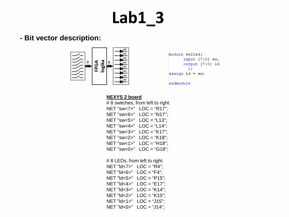
Lab1_3- Bit vector description:
NEXYS 2 board# 8 switches, from left to right NET "sw<7>" LOC = “R17";NET "sw<6>" LOC = “N17"; NET "sw<5>" LOC = “L13"; NET "sw<4>" LOC = “L14"; NET "sw<3>" LOC = “K17"; NET "sw<2>" LOC = “K18"; NET "sw<1>" LOC = “H18"; NET "sw<0>" LOC = “G18";
# 8 LEDs, from left to rightNET "ld<7>" LOC = “R4"; NET "ld<6>" LOC = “F4"; NET "ld<5>" LOC = “P15"; NET "ld<4>" LOC = “E17"; NET "ld<3>" LOC = “K14"; NET "ld<2>" LOC = “K15"; NET "ld<1>" LOC = “J15"; NET "ld<0>" LOC = “J14";
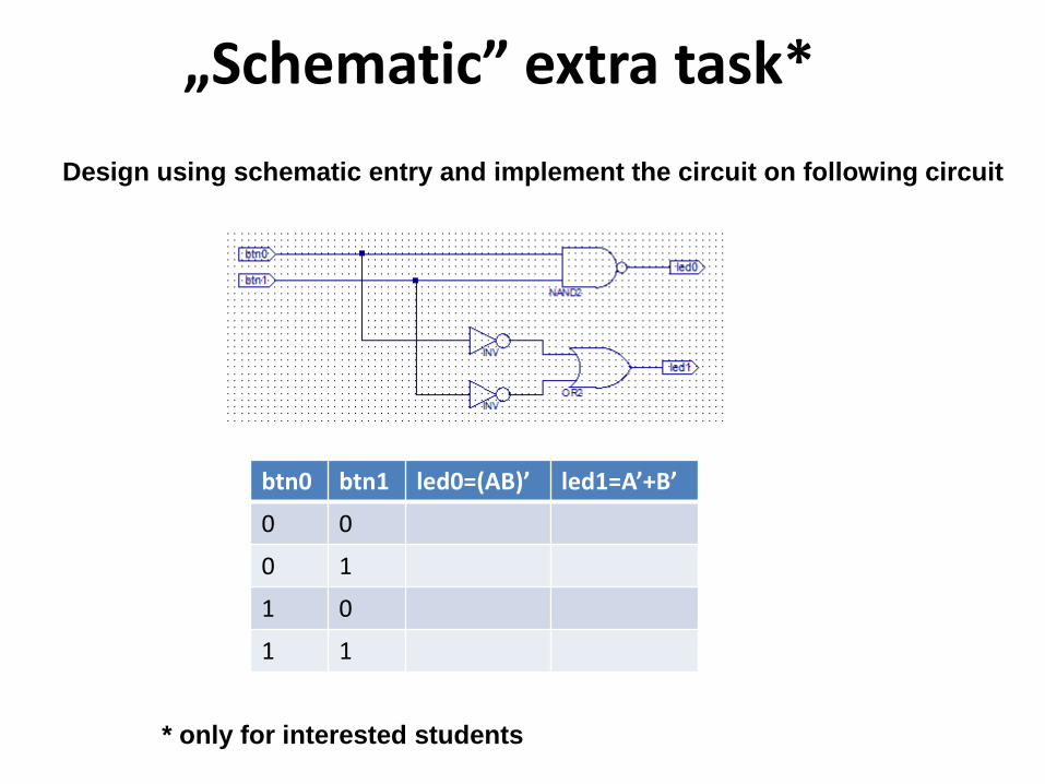
„Schematic” extra task*
btn0 btn1 led0=(AB)’ led1=A’+B’
0 0
0 1
1 0
1 1
* only for interested students
Design using schematic entry and implement the circuit on following circuit
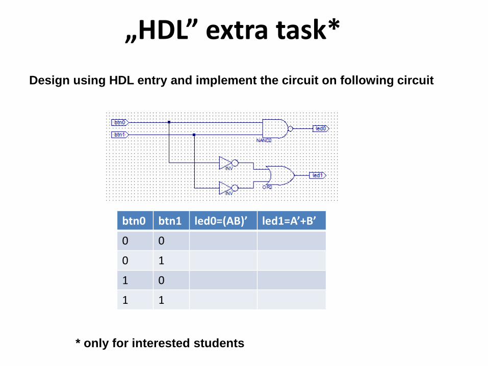
„HDL” extra task*
btn0 btn1 led0=(AB)’ led1=A’+B’
0 0
0 1
1 0
1 1
* only for interested students
Design using HDL entry and implement the circuit on following circuit


![Szakdolgozat Peter Mercse - shrek.unideb.hushrek.unideb.hu/~onigai/Szakdolgozatok/2015-2016... · 'heuhfhql (j\hwhp ,qirupdwlndl .du 2nrvrwwkrq yh]puopv phjydoyvtwivd )3*$ vhjtwvpjpyho](https://img.dokumen.tips/doc/110x75/5f9b6b4cfa0fd7599f32a341/szakdolgozat-peter-mercse-shrek-onigaiszakdolgozatok2015-2016-heuhfhql.jpg)
![[Sample Course Title Slide Insert Presentation Title]onigai/DT/DT_1.pdf · 2019. 2. 12. · Elektronika • Számonkérés ... Procesare digitala Convertor (digital) (analogic) (analogic)](https://img.dokumen.tips/doc/110x75/60af99169e357b30957d0026/sample-course-title-slide-insert-presentation-title-onigaidtdt1pdf-2019.jpg)


![[Sample Course Title Slide Insert Presentation Title]onigai/DT/DT_11.pdf · • Megjelent a LE/LC elnevezés. Logic Element/Logic Cell • Ez maradhatna a legjobb referencia 1 LUT](https://img.dokumen.tips/doc/110x75/5e412adceeacde55815791ee/sample-course-title-slide-insert-presentation-title-onigaidtdt11pdf-a.jpg)


