Embed Size (px)
Citation preview
Floating point division using the Altera MAX2PLUS package to de-sign, analyse and prove the system (IEEE754 24-bit format).
COURSE: BEng (HONS) Electronic Systems MODULE: EEE508J1 - Electronic Circuit Design BY: Colin K McCord DATE: Thursday, 17 July 2003
Digital Coursework

Thursday, 17 July 2003 Digital Coursework – Floating Point Division Colin K McCord
EEE508J1 – Electronic Circuit Design 98425145
CONTENTS
1. Introduction Page 1 2. Background Information Pages 2 to 7 2.1. IEEE 754-1990 (24-bit Version) Pages 2 to 4 2.2. ASM (Algorithmic State Machine) Charts Pages 4 to 5 2.3. Pentium Bug Pages 6 to 7 3. IEEE-754 (24-bit) Floating point Divider Pages 8 to 9
4. IEEE-754 (24-bit) Floating point Divider - Design Pages 10 to 26 4.1. fp_divide_top.gdf (IEEE-754 Floating Point Divider) Pages 10 to 11 4.2. from_ieee.gdf ( Convert From IEEE) Page 11 4.3. 8bitsub_exc127.gdf (Excess 127 – 8-bit subtraction) Pages 11 to 12 4.4. 8-bit_sub.gdf (8-bit 2’s Complement Subtraction) Pages 12 to 13 4.5. 8-bit_adder.gdf (8-bit Full Adder) Pages 13 to 14 4.6. full_adder.gdf (Full Adder) Pages 14 to 15 4.7. int_divide.gdf (Integer Divider) Pages 15 to 16 4.8. normalize.gdf (Normalize Mantissa and Exponent) Pages 16 to 17 4.9. 4counter.gdf (4-bit Synchronous Binary Up Counter) Page 18 4.10. norm_ctrl_logic.gdf (Normalising Control Logic) Pages 19 to 20 4.11. iszero.gdf (Does M[15..0] Equal Zero?) Page 20 4.12. mux4.gdf (Four Line Multiplexer) Page 21 4.13. 16-bit_shiftreg.gdf (16-bit Configurable Shift Left Register) Page 22 4.14. 4_bit_shiftreg.gdf (4-bit Configurable Shift Left Register) Page 23 4.15. norm_exp.gdf (Normalize Exponent) Pages 24 to 25 4.16. latch8.gdf (8-bit Latch) Page 25 4.17. to_ieee.gdf (Convert to IEEE) Page 26 5. IEEE-754 (24-bit) Floating point Divider - Simulation Pages 27 to 37 5.1. fp_divide_top.gdf (IEEE-754 Floating Point Divider) Pages 27 to 29 5.2. from_ieee.gdf ( Convert From IEEE) Page 30 5.3. 8bitsub_exc127.gdf (Excess 127 – 8-bit subtraction) Page 31 5.4. 8-bit_sub.gdf (8-bit 2’s Complement Subtraction) Page 31 5.5. 8-bit_adder.gdf (8-bit Full Adder) Pages 31 to 32 5.6. full_adder.gdf (Full Adder) Pages 32 to 33 5.7. int_divide.gdf (Integer Divider) Pages 33 to 34 5.8. normalize.gdf (Normalize Mantissa and Exponent) Pages 34 to 35 5.9. 4counter.gdf (4-bit Synchronous Binary Up Counter) Page 36 5.10. 16-bit_shiftreg.gdf (16-bit Configurable Shift Left Register) Page 36 5.11. to_ieee.gdf (Convert to IEEE) Page 37 6. Conclusions Pages 38 to 41
Appendixes Pages 42 to 50 A1. Hierarchy Chart for fp_divide_top.gdf Pages 42 A2. fp_divide_top.pin Page 43 to 45 A3. Conversion of Decimal to IEEE-754 – JAVA Script Page 46 A4. Conversion of IEEE-754 to Decimal – JAVA Script Page 47 A5. Floating Point Pipelined Divider – Commercial Example Pages 48 to 49 A6. CD-ROM – Containing Design and Simulation Files Page 50

Thursday, 17 July 2003 Digital Coursework – Floating Point Division Colin K McCord
EEE508J1 – Electronic Circuit Design Page 1 98425145
1 INTRODUCTION The propose of this assignment is to use the Altera Max2Plus package to design, analyse and prove working a system that can perform floating point division. The floating point numbers comply with the IEEE-754 standard for 24-bit numbers (a modified version of the 32-bit standard).
Figure 1.0a: Altera Max2Plus Software Application
The MAX+PLUS®II development software is a fully integrated programmable logic design environment. This easy-to-use tool supports the Altera® ACEX™, FLEX® and MAX® programmable device families and works in both PC and UNIX environments. The MAX+PLUS II software offers unmatched flexibility and performance and allows for seamless integration with industry-standard design entry, synthesis, and verification tools. By giving the designer entry freedom and the ability to mix and match design entry methodologies, the MAX+PLUS II software minimizes re-design work. This report includes schematic capture and other design details, as well as an English description on how the design works. The design is partitioned into functional blocks, each block does one task that is easy to describe. As well as the design details, the simulation details are included for most functional blocks within the design. The simulation results are explained, this is done by annotating the waveforms produced by the system. The report is split into 7 sections for clarity (including this introduction): -
1. Introduction. 2. Background Information. 3. IEEE-754 (24-bit) Floating Point Divider. 4. IEEE-754 (24-bit) Floating Point Divider – Design. 5. IEEE-754 (24-bit) Floating Point Divider – Simulation. 6. Conclusions. 7. Appendixes.
Commercial IEEE-754 floating point divider units exist; “Digital Core Design” DFPDIV is available for purchase and is compatible with Max2Plus (see Appendix 5, for details).
Figure 1.0b: “Digital Core Design” DFPDIV
The CD-ROM attached to appendix 6, contains all the Max2Plus design, symbol and simulation files for the designed IEEE-754 floating point divider (24-bit version).

Thursday, 17 July 2003 Digital Coursework – Floating Point Division Colin K McCord
EEE508J1 – Electronic Circuit Design Page 2 98425145
2 BACKGROUND INFORMATION 2.1: IEEE 754-1990 (24-bit Version) IEEE 754-1990 standard for binary floating point arithmetic defined what is commonly referred to as “c” N = 1.F x 2E-127 (N = Floating point number, F = fraction part in binary notation, E = exponent in bias 127 representation). In the 24 bit IEEE format, 1 is allocated as the sign bit, the next 8 bits are allocated as the exponent field, and the last 15 bits are the fractional parts of the normalised number. 23 22 21 20 19 18 17 16 15 14 13 12 11 10 9 8 7 6 5 4 3 2 1 0 - - - - - - - - - - - - - - - - - - - - - - - - S Exponent Mantissa
Figure 2.1a: IEEE-754 (24-bit version) A sign bit of 0 indicates a positive number, and a 1 is negative. The exponent field is represented by ‘excess 127 notation’. The 15 fraction bits actually represent 16 bits of precisions, as a leading 1 in front of the decimal point is implied. There are some exceptions: - E = 255; F = 0; ± infinity E = 255; F != 0; NaN, Not a number. Overflow, error… E = 0; F = 0; 0 E = 0; F != 0; denormalised, tiny number, smaller than smallest allowed. With exponent field 00000000 and 11111111 reserved, the range is restricted to 2-126 to 2127. Example: Convert 0.085 to IEEE-754 (24-bit) 1. The first step is to look at the sign of the number. Because 0.085 is positive, the sign bit = 0. 2. Write 0.085 in base-2 scientific notation. This means that the number must be factored in the range [1<= n <2] and a power of 2. 0.085 = (-1)0 * (1+fraction) * 2power, or 0.085 / 2power = (1+fraction). 0.085 / 2-1 = 0.17 0.085 / 2-2 = 0.34 0.085 / 2-3 = 0.68 0.085 / 2-4 = 1.36 Therefore, 0.085 = 1.36 x 2-4 3. Find the exponent. The power of 2 is -4, and the bias is 127, hence exponent = 12310 or 0111110112.

Thursday, 17 July 2003 Digital Coursework – Floating Point Division Colin K McCord
EEE508J1 – Electronic Circuit Design Page 3 98425145
4. Write the fraction in binary form.
The fraction = 0.36. Unfortunately, this is not a ‘pretty’ number, like those shown in most text books. The best that can be done is to approximate the value. Binary fractions look like this: -
0.1 = (1/2) = 2-1 0.01 = (1/4) = 2-2 0.001 = (1/8) = 2-3
To approximate 0.36: - 0.36 = (0/2) + (1/4) + (0/8) + (1/16) + (1/32) + … 0.36 = 2-2 + 2-4 + 2-5 + … 0.3610 ≈ 0.0101110000101002 It’s important to notice that 0.36 cannot be represented exactly in the IEEE-754 format. 5. Now put the binary strings in the correct order. 1 bit for the sign, followed by 8 for the exponent, and 15 for the fraction. The answer is: -
23 22 21 20 19 18 17 16 15 14 13 12 11 10 9 8 7 6 5 4 3 2 1 0 0 0 1 1 1 1 0 1 1 0 1 0 1 1 1 0 0 0 0 1 0 1 0 0 S Exponent Mantissa
Figure 2.1b: IEEE-754 representation of 0.085 Example: Convert IEEE-754 (24-bit) Figure 2.1c to a Float 23 22 21 20 19 18 17 16 15 14 13 12 11 10 9 8 7 6 5 4 3 2 1 0 1 1 0 0 0 0 0 0 1 1 0 1 1 0 0 1 1 0 0 1 1 0 0 1 S Exponent Mantissa
Figure 2.1c: IEEE-754 (24-bit version) Number 1. First put the bits in three groups. Bit 23 shows the sign of the number. Bits 22-15 are the exponent. Bits 14-0 give the fraction. 2. Now, look at the sign bit. If this bit is a 1, the number is negative. If it is 0, the number is positive. This bit is 1, so the number is negative. 3. Get the exponent and the correct bias. The exponent is simply a positive binary number 100000012 = 12910. Remember that the bias (127) must be subtracted from this exponent to find the power of 2.

Thursday, 17 July 2003 Digital Coursework – Floating Point Division Colin K McCord
EEE508J1 – Electronic Circuit Design Page 4 98425145
4. Convert the fraction string into base ten. This is the trickiest step. The binary string represents a fraction, so conversion is a little different. Binary fraction look like this: -
0.1 = (1/2) = 2-1 0.01 = (1/4) = 2-2 0.001 = (1/8) = 2-3
So, for this example, multiply each digit by the corresponding power of 2. 0.11000000011011001100110012 = 1 x 2-1 + 0 x 2-2 + 1 x 2-3 + 1 x 2-4 + 0 x 2-5 + 0 x 26 + … 0.11000000011011001100110012 = 1/2 + 1/8 + 1/16 + …
Note that this number is just a approximation on some decimal number. There will most likely to be some error. In this case the fraction is about 0.7000000476837158.
5. This is all the information that is required to put these numbers in the expression. N = 1.F x 2E-127
N = 1.7000000476837158 x 2129-127 ≈ 6.8 S = 1, hence the answer is approximately -6.8. 2.2: ASM (Algorithmic State Machine) Charts ASM charts are similar to flow charts and offer several advantages over state diagrams. Main features of ASM charts: -
• Operation of a digital system represented by an ASM chart is easier to understand as compared to its table/state diagram.
• An ASM chart can be converted into several equivalent forms and each form leads directly to a
hardware realisation.
• The conditions for a proper state diagram are completely satisfied by the ASM chart.
• ASM chart based digital system design and representation is equivalent to software design. The state diagram/table based design approach becomes impractical for systems with large number of inputs: -
• The number of columns for the state table doubles with every additional input. • All the inputs are not relevant at each clock pulse/transition (don’t care conditions). On the other
hand, the ASM approach only shows the active inputs on the chart.
• State diagrams are not flexible enough in terms of describing very complex FSMs.
• State diagrams are not suitable for gradual refinement of FSM.
Thursday, 17 July 2003 Digital Coursework – Floating Point Division Colin K McCord
EEE508J1 – Electronic Circuit Design Page 5 98425145
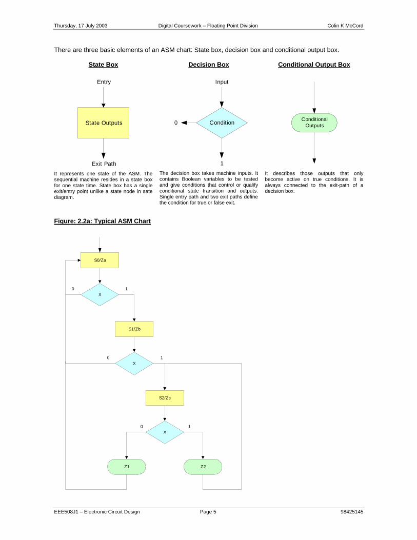
There are three basic elements of an ASM chart: State box, decision box and conditional output box.
State Box
Decision Box Conditional Output Box
State Outputs
Entry
Exit Path
It represents one state of the ASM. The sequential machine resides in a state box for one state time. State box has a single exit/entry point unlike a state node in sate diagram.
Condition
Input
1
0
The decision box takes machine inputs. It contains Boolean variables to be tested and give conditions that control or qualify conditional state transition and outputs. Single entry path and two exit paths define the condition for true or false exit.
ConditionalOutputs
It describes those outputs that only become active on true conditions. It is always connected to the exit-path of a decision box.
Figure: 2.2a: Typical ASM Chart
S0/Za
X0
S1/Zb
1
X0 1
S2/Zc
X
Z1 Z2
0 1

Thursday, 17 July 2003 Digital Coursework – Floating Point Division Colin K McCord
EEE508J1 – Electronic Circuit Design Page 6 98425145
2.3: Pentium Bug The original Intel Pentium processor had a bug with the floating point divider. The FPU uses the most significant bits of the divisor and the dividend / remainder to guess the next 2 bits of the quotient. This guess is taken from a lookup table: -2, -1, 0, +1, +2, if the previous guess gives a reminder which is too large the quotient is adjusted in subsequent passes of -2. Guess is multiplied by the divisor and subtracted from the remainder to generate a new remainder. This method is called SRT division, which is named after the 3 people who came up with the idea. The Pentium FPU bug was simple human error; just a few missing entries in the lookup table. The first 11 bits to the right of the decimal point are always correct, the bug can occur between bits 12 to 52 (4th to 15th decimal digits). For example in Microsoft Excel, try: -
4,195,835 * 31457273,145,727
A computer fitted with a bug free processor will calculate the answer to be 4,195,835; while a computer fitted with the flawed Pentium will calculate the answer to be 4,195,579 (Assuming Excel doesn’t already have the SW bug patch). Success of the IEEE standard made the discovery possible, e.g. all computers should get the same answer. Intel’s Pentium team ran exhaustive functional simulation, but the same engineer who wrote the RTL code for the floating-point division also wrote the simulation script. Pentium Bug Time Line June 1994: Intel discovers the bug and plans to produce bug free chips in January 1995; hence
4 to 5 million Pentiums would be produced with the bug. September 1994: Scientist suspects errors and posts on Internet. November 1994: Intel Press release: “Can make errors in 9th digit… Most engineers and financial
analysts need only 4 to 5 digits. Theoretical mathematicians should be concerned. … So far only heard from one.”
Intel claims it happens once in 27,000 years for typical spreadsheet users (1000
divides / day X error rate assuming numbers are random). December 1994: IBM claims it happens once per 24 days and bans Pentium sales; Intel said it
regards IBM’s decision to halt shipments of its Pentium processor-based systems as unwarranted.
Pentium Jokes Q: What’s another name for the “Intel Inside” sticker they put on Pentiums? A: Warning label. Q: Have you heard the new name Intel has chosen for the Pentium? A: The Intel inacura. Q: According to Intel, the Pentium conforms to the IEEE standards for floating point arithmetic. If you fly in an
aircraft designed using a Pentium, what is the correct pronunciation of “IEEE”? A: Aaaaaaaaiiiiiiiiieeeeeeeeeeeeeeeeeeeee!

Thursday, 17 July 2003 Digital Coursework – Floating Point Division Colin K McCord
EEE508J1 – Electronic Circuit Design Page 7 98425145
Pentium Conclusion: Dec. 21, 1994 $500M Write-Off “To owners of Pentium processor-based computers and the PC community: We at Intel wish to sincerely apologize for our handling of the recently publicised Pentium processor flaw. The Intel Inside symbol means that your computer has a microprocessor second to none in quality and performance. Thousands of Intel employees work very hard to ensure that this is true. But no microprocessor is ever perfect. What Intel continues to believe is technically an extremely minor problem has taken on a life of its own. Although Intel firmly stands behind the quality of the current version of the Pentium processor, we recognise that many users have concerns. We want to resolve these concerns. Intel will exchange the current version of the Pentium processor for an updated version, in which this floating-point divide flaw is corrected, for any owner who requests it, free of charge anytime during the life of their computer. Sincerely, Andrew S. Grove President / CEO
Craig R. Barrett Executive Vice President & COO
Gordon E. Moore Chairman of the Board”

Thursday, 17 July 2003 Digital Coursework – Floating Point Division Colin K McCord
EEE508J1 – Electronic Circuit Design Page 8 98425145
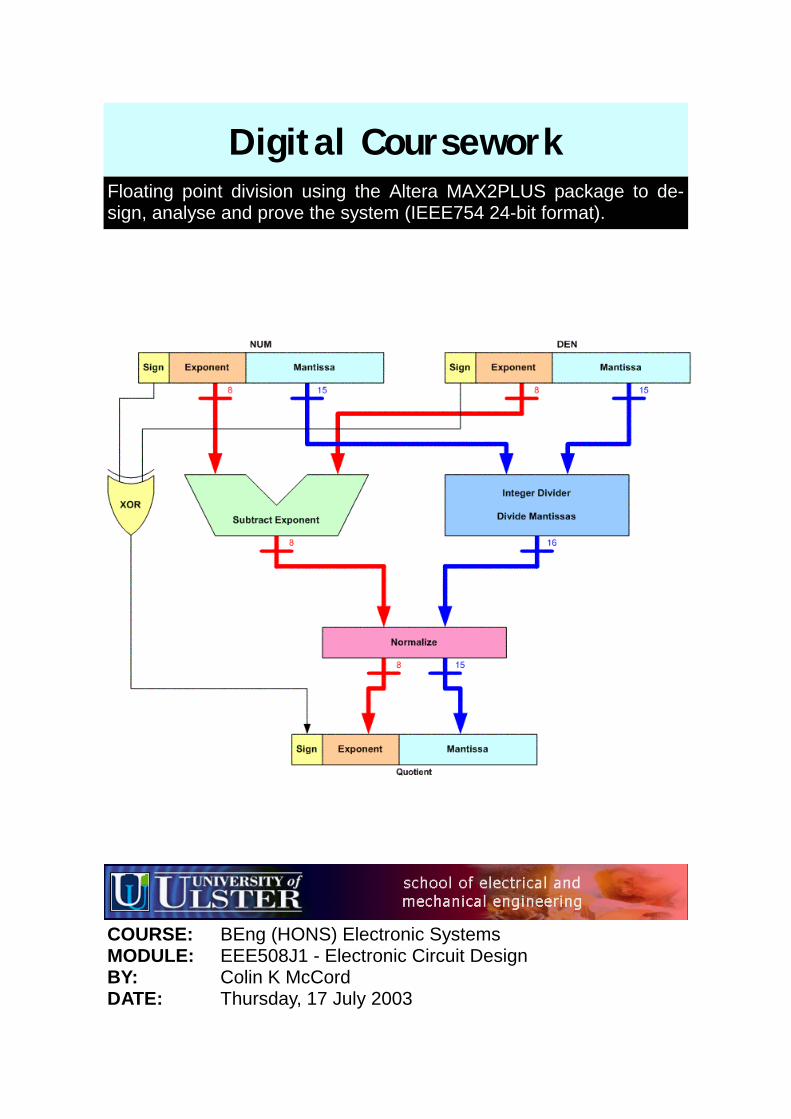
3 IEEE-754 (24-BIT) FLOATING POINT DIVIDER To divide floating point numbers, subtract the exponents and divide the mantissas. Example divide 55 x 105 by 5 x 10-2: -
5
72
54 654 10 9 6 109 10 5 ( 2) 7
Quot−
=×⇒ ⇒ = ×
× − − =
Sign Exponent Mantissa
Sign Exponent Mantissa
DEN
8 815
Sign Exponent Mantissa
NUM
15
Integer Divider
Divide Mantissas
16
Subtract Exponent
8
Quotient
Normalize
158
XOR
Figure 3.0a: Floating Point Divider Core NUM, DEN and Quotient are in the standard IEEE-754 (24-bit) format. An XOR takes care of the sign bit, and an excess 127 subtract (e.g. a-b+127) takes care of the Exponent. A 15-bit integer divider will not produce accurate results, hence internally the num is extend to 32-bits (bit 31 = 1, bits 30 to 16 = ‘NUM mantissa’, and bits 15 to 0 = 0) and the DEN is extend to 16-bits (bit 15 = 1, bits 14 to 0 = ‘DEN mantissa’). Recall that there is always a hidden MSB ‘1’ according to the IEEE-754 standard, this ‘1’ must be included in the calculation, hence the reason why MSB ‘1’s have been hardwired into both the num and the den. This ‘1’ must be removed during the normalising process, hence the reason why a 16-bit mantissa is inputted into the normalize block and a 15-bit mantissa is outputted. Because MSB ‘1’s are hardwired, the quotient is never any more than 17-bits wide, the LSB is dropped and bits 16 to 1 are sent to the normalize block.
Thursday, 17 July 2003 Digital Coursework – Floating Point Division Colin K McCord
EEE508J1 – Electronic Circuit Design Page 9 98425145
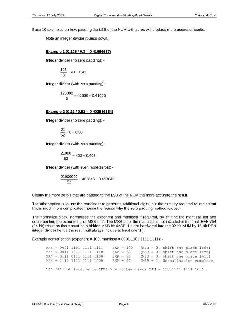
Base 10 examples on how padding the LSB of the NUM with zeros will produce more accurate results: - Note an integer divider rounds down. Example 1 (0.125 / 0.3 = 0.41666667) Integer divider (no zero padding): -
125 41 0.413
= =
Integer divider (with zero padding): -
125000 41666 0.416663
= =
Example 2 (0.21 / 0.52 = 0.403846154) Integer divider (no zero padding): -
21 0 0.0052
= =
Integer divider (with zero padding): -
21000 403 0.40352
= =
Integer divider (with even more zeros): -
21000000 403846 0.40384652
= =
Clearly the more zero’s that are padded to the LSB of the NUM the more accurate the result. The other option is to use the remainder to generate additional digits, but the circuitry required to implement this is much more complicated, hence the reason why the zero padding method is used. The normalize block, normalises the exponent and mantissa if required, by shifting the mantissa left and decrementing the exponent until MSB = ‘1’. The MSB bit of the mantissa is not included in the final IEEE-754 (24-bit) result as there must be a hidden MSB bit (MSB ‘1’s are hardwired into the 32-bit NUM by 16-bit DEN integer divider hence the result will always include at least one ‘1’). Example normalisation (exponent = 100, mantissa = 0001 1101 1111 1111): - MAN = 0001 1101 1111 1111 EXP = 100 (MSB = 0, shift one place left) MAN = 0011 1011 1111 1110 EXP = 99 (MSB = 0, shift one place left) MAN = 0111 0111 1111 1100 EXP = 98 (MSB = 0, shift one place left) MAN = 1110 1111 1111 1000 EXP = 97 (MSB = 1, Normalisation complete) MSB ‘1’ not include in IEEE-754 number hence MAN = 110 1111 1111 1000.

Thursday, 17 July 2003 Digital Coursework – Floating Point Division Colin K McCord
EEE508J1 – Electronic Circuit Design Page 10 98425145
4 IEEE-754 (24-BIT) FLOATING POINT DIVIDER – DESIGN 4.1: fp_divide_top.gdf (IEEE-754 Floating Point Divider)
Figure 4.1a: Screen dump of fp_divide_top.gdf
Notice the design has been partitioned into a number of functional blocks, each block does one task that can be easily described. This partitioned method of design makes the design and testing of large complex machines easy. Each functional block is tested using simulation, then when all blocks are working as designed the entree system is tested. Note that the design of a functional block can be made-up by other functional blocks, which in turn may have blocks within them; this cycle continues until there are no more functional blocks. Clearly even the most complex of designs can be simplified dramatically, using this partition method. The symbols of the functional blocks shown in figure 4.1a have been customised to make the circuit more user-friendly. The functional block ‘from_ieee’ separates an IEEE-754 24-bit number into its key components: sign bit (b23), exponent (b22-b15) and mantissa (b14 – b0). There are two ‘from_ieee’ blocks in the design, the IEEE numerator input is fed into one (block 77), while the IEEE denominator input is fed into the other (block 78). The functional block ‘8bitsub_exc127’ subtracts the denominator exponent from the numerator exponent and adds 127 (numEXP – denEXP + 127). Block ‘int_divide’ divides the denominator mantissa into the numerator mantissa (numM / denM).

Thursday, 17 July 2003 Digital Coursework – Floating Point Division Colin K McCord
EEE508J1 – Electronic Circuit Design Page 11 98425145
The result of the subtraction of the exponents RES[7..0] and the result of the division of the mantissas QUOT[15..0] is fed into the ‘normalize’ block. This block normalises, by shifting the mantissa left and decrementing the exponent if required. Notice that there are three other inputs which are connected to input pins: CLK should be connected to a clock, RESET will reset all flip-flops (active low), EN enables/disables calculation (1 for enable, 0 for disable). Notice that there is also an additional output connected to an output pin called ‘VAILD’ this will go high if the calculation is finished and the output data is valid else it will stay low. A 2-input XOR gate is fed by the sign-bit of the numerator and sign-bit of the denominator. The functional block ‘to_ieee’ merges the key components, sign, exponent and mantissa back into the IEEE-754 24-bit format. The normalised exponent EO[7..0], normalised mantissa MO[14..0] and the output of the XOR gate is fed into the ‘to_ieee’ block. The output is connect to the QUOT[23..0] pin, which contains the result of the floating point division, which is in the standard IEEE-754 24-bit format (only valid when VALID pin is high). 4.2: from_ieee.gdf (Convert From IEEE)
Figure 4.2a: Screen dump of from_ieee.gdf
Separates an IEEE-754 24-bit number into its key components: sign bit (b23), exponent (b22-b15) and mantissa (b14 – b0). Bit-23 (IEEE23) is connected to output SIGN, bits 22 to 15 (IEEE[22..15]) are connected to output E[7..0] (exponent) and bits 14 to 0 (IEEE[14..0]) are connect to output M[14..0] (mantissa). Altera’s ‘bus2bus’ parameterized mega-function (found in mega_lpm library) is used to connect bus-lines. 4.3: 8bitsub_exc127.gdf (Excess 127 – 8-bit Subtraction) The function of this block is to subtract b[7..0] from a[7..0] and add 127: -
RES[7..0] = a[7..0] – b[7..0] + 127. Obviously the reason for adding 127 is that IEEE exponent numbers have 127 added to them, if two of these numbers are subtracted the 127 bias is removed and must be restored for the result to be valid. Figure 4.3a shows the design of this block, clearly it is extremely simple. Basically an 8-bit subtraction block is used to subtract b[7..0] from a[7..0] with the result being fed into an 8-bit addition block and added with 127 (or 01111111 in binary). The result of the addition block is fed to output pin RES[7..0].

Thursday, 17 July 2003 Digital Coursework – Floating Point Division Colin K McCord
EEE508J1 – Electronic Circuit Design Page 12 98425145
Figure 4.3a: Screen dump of 8bitsub_exc127.gdf
4.4: 8-bit_sub.gdf (8-bit 2’s Complement Subtraction)
Figure 4.4a: Screen dump of 8-bit_sub.gdf
The function of this block is to subtract B[7..0] from A[7..0]. The simplest way of subtracting two numbers using logic gates is to take the 2’s complement (convert from positive to negative) of the number being subtracted and then add them.

Thursday, 17 July 2003 Digital Coursework – Floating Point Division Colin K McCord
EEE508J1 – Electronic Circuit Design Page 13 98425145
Converting a positive binary number to a negative binary 2’s complement number is easy, first complement each bit e.g. convert the ‘1’s to ‘0’s and ‘0’s to ‘1’s (this is known as one’s complement), then add 1 (two’s complement). For example convert 3510 to -3510 two’s complement: -
10 2
2
2
10 2
35 00100011One's complement 11011100
Add 1 1Two's complement (-35 ) 11011101
=
=
= +
=
Example subtraction, 18 – 7 e.g. 18 + (-7): -
10 2
10 2
2 10
18 000100107 11111001
sum 00001011 11
=
− =
= =
Figure 4.3b shows the design of this block, A[7..0] is fed directly into the 8-bit adder. B[7..0] is inverted using a series of NOT gates (one’s complement) then fed into the 8-bit adder. The CIN (carry in) input of the adder is used to add 1 (two’s complement), and the result is connect to the output pin A-B[7..0]. 4.5: 8-bit_adder.gdf (8-bit Full Adder)
Figure 4.5a: Screen dump of 8-bit_adder.gdf
The function of this block is to add A[7..0] and B[7..0], the result of this addition is fed to the output SUM[7..0]. Input pin Cin (carry in) and Cout (carry out) are useful, as they can be used to daisy chain a number of 8-bit adders together to make a 16,24,32,… bit adder. Clearly the adder is made up by daisy chaining 8 full-adders, e.g. Input pin Cin is connected to the carry-in of the LSB full-adder and the carry-out becomes the carry-in of the next full-adder, and the carry-out of the next

Thursday, 17 July 2003 Digital Coursework – Floating Point Division Colin K McCord
EEE508J1 – Electronic Circuit Design Page 14 98425145
full-adder becomes the carry-in of the one following the next etc.... The carry-out of the MSB full-adder is connected to output pin Cout. 4.6: full_adder.gdf (Full Adder)
Figure 4.6a: Screen dump of full_adder.gdf
The operation of this block is to add A & B; a standard logic design that can be found in many text books is used, which uses 2 XOR gates, 2 AND gates, and 1 OR gate.
A B Cin Sum Cout 0 0 0 0 0 0 0 1 1 0 0 1 0 1 0 0 1 1 0 1 1 0 0 1 0 1 0 1 0 1 1 1 0 0 1 1 1 1 1 1
Figure 4.6b: Full adder truth table Look at the truth table (figure 4.6b); for what input condition is the sum output HIGH? The answer is that the sum bit is HIGH whenever the three inputs (A,B.Cin) are odd. An even-parity generator produces a HIGH output whenever the sum of the inputs is odd, hence an even-parity generator can be used to generate the sum output bit, as shown in figure 4.6c.
AB
CinSum = 1 forodd numberof HIGHinputs
Figure 4.6c: The sum function of the full-adder is generated from an even-parity generator.
How about the carry-out bit? What input conditions produce a HIGH at Cout? The answer is that Cout is HIGH whenever any two of the inputs are HIGH. Therefore three ANDs and an OR can take care of Cout, as shown in figure 4.6d.

Thursday, 17 July 2003 Digital Coursework – Floating Point Division Colin K McCord
EEE508J1 – Electronic Circuit Design Page 15 98425145
AB
ACin
BCin
Cout = 1for anytwoinputHIGH
Figure 4.6d: Carry-out (Cout) function of the full-adder.
The two parts of the full-adder circuit shown in figures 4.6c and 4.6d can be combined to form the complete full-adder circuit shown in figure 4.6a. In figure 4.6a the sum function is produced using the same logic as that in figure 4.6c (an XOR feeding an XOR). The cout function comes from AB or ( )Cin AB AB+ . 4.7: int_divide.gdf (Integer Divider)
Figure 4.7a: Screen dump of int_divide.gdf
This is block is not a normal integer divider; it is specially designed for dividing the mantissas of two IEEE-754 (24-bit) floating point numbers. The LPM_DIVIDE parameterized mega-function is used to carry out the divide operation, notice that LPM_PIPELINE = 0 which means the divider is purely combinatorial logic. Note that the numer[] and Quotient[] of the divider are 32-bits wide and the denom[] and remain[] are 16-bits wide. Recall that the IEEE-754 standard removes the MSB ‘1’ of the mantissas, which must be included in the divide calculation. That’s the reason why M31 and D15 are connected to VCC. NUM[14..0] is extended to 32-bits, by 0’s to the right of the least significant bit. The bus2bus parameterized mega-function is used to connect N[15..0] to GND and NUM[14..0] to N[30..16]. Q[16..1] is connected via bus2bus to QUOT[15..0], clearly all bits larger than Q16 will always be zero, but the LSB Q0 will be lost; not important as it’s the LSB.

Thursday, 17 July 2003 Digital Coursework – Floating Point Division Colin K McCord
EEE508J1 – Electronic Circuit Design Page 16 98425145
The largest possible quotient value: -
NUM[14..0] = 111 1111 1111 1111 DEN[14..0] = 000 0000 0000 0000 N[31..0] = 1111 1111 1111 1111 0000 0000 0000 0000 (1 hard-wired) D[15..0] = 1000 0000 0000 0000 (1 hard-wired) Q[31…0] = 0000 0000 0000 0001 1111 1111 1111 1110 (Bits used for QUOT[]) QUOT[15..0] = 1111 1111 1111 1111
The smallest possible quotient value: -
NUM[14..0] = 000 0000 0000 0000 DEN[14..0] = 111 1111 1111 1111 N[31..0] = 1000 0000 0000 0000 0000 0000 0000 0000 (1 hard-wired) D[15..0] = 1111 1111 1111 1111 (1 hard-wired) Q[31…0] = 0000 0000 0000 0000 1000 0000 0000 0000 (Bits used for QUOT[]) QUOT[15..0] = 0100 0000 0000 0000
4.8: normalize.gdf (Normalize Mantissa and Exponent)
Figure 4.8a: Screen dump of normalize.gdf
The operation of this block is complex as it is not made-up of purely combinational logic and cannot be easily described. There are 4 functional blocks, ‘norm_ctrl_logic’, ‘4counter’, ‘16_bit_shiftreg’ and ‘norm_exp’. Basically the mantissa is shifted to the left until MSB = ‘1’ and the number of shifts is subtracted from the Exponent. The MSB of the normalised mantissa is not included in EO[14..0] as the IEEE-754 standard requires the MSB ‘1’ to be hidden, hence the reason why the input mantissa is 16-bits wide and the output mantissa is 15-bits wide. The ASM (Algorithmic State Machine) method can be used in the design. There are four states 00, 01, 10 and 11, each state carries out a number of operations. Block ‘4counter’ is the state counter, and is controlled by block ‘norm_ctrl_logic’. The state counter specifies the operation of the ‘16-bit_shiftreg’ and ‘norm_exp’.

Thursday, 17 July 2003 Digital Coursework – Floating Point Division Colin K McCord
EEE508J1 – Electronic Circuit Design Page 17 98425145
Initial State
VALID = 0
EN0
Load mantissainto shift register,
and load exponentinto latch
MS15 = 0 &MZERO = 0
1
True
Shift mantissa oneplace to the left.
Zero fill LSB
DEC Exponent
MS15
S0
S1
S2
Hold shift registerand latch.
VALID = 1
S3
Clear 16-bit shiftregister (Mantissa)
and 8-bit latch(Exponent)
EN0
1
False
1
0
EN0
1
EN
1
0
Figure 4.8b: Simplified ASM Chart for ‘normalize.gdf’
Figure 4.8b shows the ASM chart of the normalising process. State 00 (S0) Output VALID is zeroed. The 16-bit shift register used for the mantissa and the 8-bit latch (inside the ‘norm_exp’ block) used for holding the exponent are cleared. If EN is ‘1’ then move to the next state, else stay here. Notice that EN and RESET are connect to a BNOR gate, its output is connected the RESET pins of blocks ‘4counter’, ’16-bit_shiftreg’ and ‘norm_exp’. Hence at any time if either becomes zero the system returns to state 00. State 01 (S1) Load mantissa M[15..0] into the 16-bit shift register and load the exponent E[7..0] into the 8-bit latch. M[15..0] is connect to the L[15..0] input of the ’16-bit_shiftreg’ and E[7..0] is connected to ‘norm_exp’. IF MS15 = 0 and MZERO = 0 then move to the next state. Notice MS15 is inputted into the ‘norm_ctrl_logic’ block and MZERO is an output of this block. If MS15 = 1 or MZERO = 1, the state counter stills moves to state 01, but notice the NOSHIFT flag from the ‘norm_ctrl_logic’ block. This forces blocks ’16-bit-shftreg’ and ‘norm_exp’ into state 11. State 10 (S2) Output NEXTSTATE form the ‘norm_ctrl_logic’ block will be zero if BS15 is zero. Therefore the state counter will be disabled and will stay at state 10. Block ’16-bit_shiftreg’ shifts one place to the left, and block ‘norm_exp’ DECs the exponent. This cycle continues on every clock plus, until BS15 is ‘1’. If BS15 is ‘1’ the output NEXTSTATE of the ‘norm_ctrl_logic’ block will be ‘1’. Therefore the state counter is enabled and will move to state 11. State 11 (S3) Holds normalised exponent and normalised mantissa and sets output flag VALD.

Thursday, 17 July 2003 Digital Coursework – Floating Point Division Colin K McCord
EEE508J1 – Electronic Circuit Design Page 18 98425145
4.9: 4counter.gdf (4-bit Synchronous Binary Up Counter)
Figure 4.9a: Screen dump of 4counter.gdf
Ripple counters have a problem due to the accumulated propagation delay of the clock from flip-flop to flip-flop. Synchronous counters eliminate that problem, because all the clock inputs are tied to a common clock, so each flip-flop will be triggered at the same time (thus any Q output transitions will occur at the same time). To design a 4-bit synchronous counter four flip-flops (JK in this case) are required. Keep in mind that, because all the clock inputs receive a trigger at the same time, certain flip-flops must be stopped from making output transitions until it is their turn. To keep the appropriate flip-flops in the hold condition or toggle condition, their J and K inputs are tied together and, through the use of additional AND gates, as shown in figure 4.9a, the J and K inputs will be both be 0 or 1, depending on whether they are to be in the hold or toggle mode. From figure 4.9a it is clear that the same clock input is driving all four flip-flops. The Q1 flip-flop will be in the hold mode (J1 = K1 = 0) until Q0 goes HIGH (assuming ENABLE is also HIGH), which will force J1 and K1 HIGH, allowing the Q1 flip-flop to toggle when the next negative clock edge comes in. Flip-flop Q2 cannot toggle until Q0 and Q1 are both HIGH (ENABLE must also be HIGH). Flip-flop Q3 cannot toggle until Q0, Q1 and Q2 are all HIGH (ENABLE must also be HIGH). RESET pin is connected to the CLRN of all the flip-flops, and VCC is connected to the PRN of all the flip-flops. If ENABLE is HIGH the counter counts up as normal, but if ENABLE is LOW all flip-flops are in the hold condition e.g. the count has been paused. If the count reaches 1111 the counter returns to zero on the next clock plus and starts the counting all over again. Clearly the circuit is more complicated then a standard ripple counter, but the cumulative effect of propagation delays through the flip-flops is not a problem because all output transitions will occur at the same time. There is a propagation delay through the AND gates, but it will not affect the Q outputs of the flip-flops.

Thursday, 17 July 2003 Digital Coursework – Floating Point Division Colin K McCord
EEE508J1 – Electronic Circuit Design Page 19 98425145
4.10: norm_ctrl_logic.gdf (Normalising Control Logic)
Figure 4.10a: Screen dump of norm_ctrl_logic.gdf
This functional block is spilt-up into 4 sections.
Figure 4.10b: Section 1
If mantissa M[15..0] is zero and state is 10 (shifting state) then MZERO is ‘1’, else MZERO is ‘0’.
Figure 4.10c: Section 2
If state is 10 (shifting state) and MS15 (from shift register) is 1 then NOSHIFT is 1, else NOSHIFT equals S0.
Thursday, 17 July 2003 Digital Coursework – Floating Point Division Colin K McCord
EEE508J1 – Electronic Circuit Design Page 20 98425145
Figure 4.10d: Section 3
If in the holding state (S0 = 1, S1 = 1) normalising is complete, and the VALID flag is set.
Figure 4.10e: Section 4
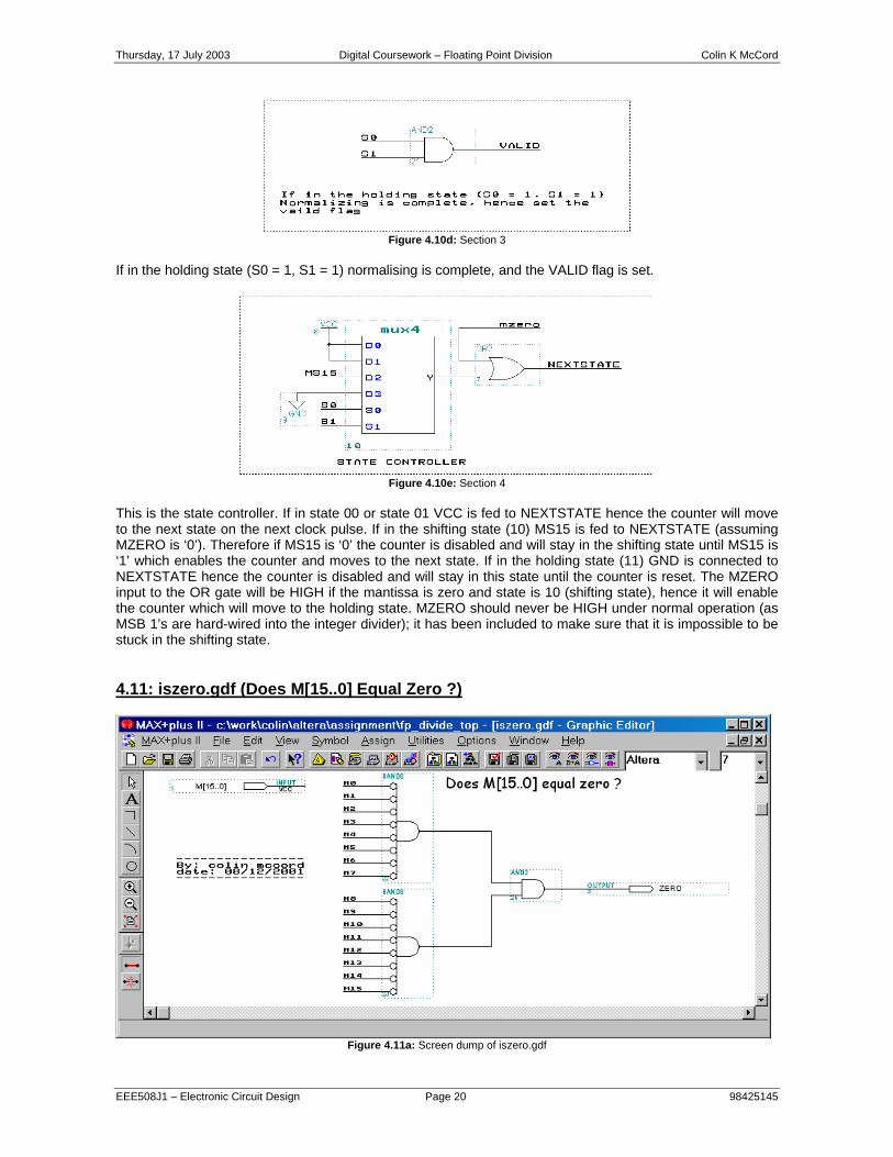
This is the state controller. If in state 00 or state 01 VCC is fed to NEXTSTATE hence the counter will move to the next state on the next clock pulse. If in the shifting state (10) MS15 is fed to NEXTSTATE (assuming MZERO is ‘0’). Therefore if MS15 is ‘0’ the counter is disabled and will stay in the shifting state until MS15 is ‘1’ which enables the counter and moves to the next state. If in the holding state (11) GND is connected to NEXTSTATE hence the counter is disabled and will stay in this state until the counter is reset. The MZERO input to the OR gate will be HIGH if the mantissa is zero and state is 10 (shifting state), hence it will enable the counter which will move to the holding state. MZERO should never be HIGH under normal operation (as MSB 1’s are hard-wired into the integer divider); it has been included to make sure that it is impossible to be stuck in the shifting state. 4.11: iszero.gdf (Does M[15..0] Equal Zero ?)
Figure 4.11a: Screen dump of iszero.gdf

Thursday, 17 July 2003 Digital Coursework – Floating Point Division Colin K McCord
EEE508J1 – Electronic Circuit Design Page 21 98425145
4.12: mux4.gdf (Four Line Multiplexer)
Figure 4.12a: Screen dump of mux4.gdf
A multiplexer is a device capable of funnelling several data lines into a single line for transmission to another point. The multiplexer has two or more digital input signals connected to its input. Control signals are also input to tell which data-input line to select for transmission. Figure 4.12a shows a simple four-line multiplexer built from SSI logic gates. The control inputs (S1, S0) take care of enabling the correct AND gate to pass just one of the data inputs through to the output.

Thursday, 17 July 2003 Digital Coursework – Floating Point Division Colin K McCord
EEE508J1 – Electronic Circuit Design Page 22 98425145
4.13: 16-bit_shiftreg.gdf (16-bit Configurable Shift Left Register)
Figure 4.13a: Screen dump of 16-bit_shiftreg.gdf
Four 4-bit configurable shift left registers are daisy chained together. Input CLK is connected to the CLK of all shift registers, and Input RESET is connected to the RESET of all shift registers. The shift registers have four functions: Reset, Load, Shift left and Hold. If S1 = 0 and S0 = 0 all of the shift registers are reset. If S1 = 0 and S1 = 1; Shift register 1 loads L[3..0], Shift register 2 loads L[7..4], Shift register 3 loads L[11..8] and shift register 4 load L[15.. 12]. If S1=1 and S1 = 0, all shift registers shift one place to the left on every clock pulse. Notice that Q-1 of shift register 1 is connected to GND, e.g. zeros are filled in, Q-1 of shift register 2 is connected to Q3, Q-1 of shift register 3 is connected to Q7 and Q-1 of shift register 4 is connected to Q11. If S1 = 1 and S1 = 1 all shift registers are in the hold mode, e.g. the output remains unchanged during future clock pulses.

Thursday, 17 July 2003 Digital Coursework – Floating Point Division Colin K McCord
EEE508J1 – Electronic Circuit Design Page 23 98425145
4.14: 4-bit_shiftreg.gdf (4-bit Configurable Shift Left Register)
Figure 4.14a: Screen dump of 4-bit_shiftreg.gdf
The shift register has four functions: Reset, Load, Shift left and Hold. If S1 = 0 and S0 = 0 data line D0 is selected and GND is fed into the D input of all the flip-flops. E.g. Reset If S1 = 0 and S0 = 1 data line D1 is selected: L0 is fed into flip-flop Q0, L1 is fed into flip-flop Q1, L2 is fed into flip-flop Q2 and L3 is fed into flip-flop Q3. E.g. Load If S1 = 1 and S0 = 0 data line D2 is selected: Input Q-1 is fed to flip-flop Q0, Q0 is fed into flip-flop Q1, Q1 is fed into flip-flop Q2 and Q2 is fed into flip-flop Q3. E.g. Shift left. If S1 = 1 and S0 = 1 data line D3 is selected: Q0 is fed to flip-flop Q0, Q1 is fed into flip-flop Q1, Q2 is fed into flip-flop Q2 and Q3 is fed into flip-flop Q3. E.g. Hold. D-type flip-flops are used. Input pin RESET is fed to CLRN of every flip-flop, VCC is fed to PRN of every flip-flop and input pin CLK is fed to the clock input of every flip-flop.
Thursday, 17 July 2003 Digital Coursework – Floating Point Division Colin K McCord
EEE508J1 – Electronic Circuit Design Page 24 98425145
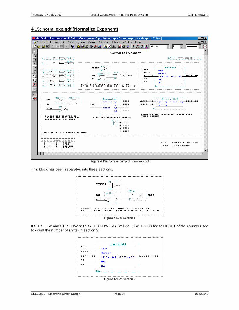
4.15: norm_exp.gdf (Normalize Exponent)
Figure 4.15a: Screen dump of norm_exp.gdf
This block has been separated into three sections.
Figure 4.15b: Section 1
If S0 is LOW and S1 is LOW or RESET is LOW, RST will go LOW. RST is fed to RESET of the counter used to count the number of shifts (in section 3).
Figure 4.15c: Section 2

Thursday, 17 July 2003 Digital Coursework – Floating Point Division Colin K McCord
EEE508J1 – Electronic Circuit Design Page 25 98425145
Section 2 contains an 8-bit latch; this latch is used to store the original exponent. RESET, CLK, E[7..0], S0, S1 are fed directly to the latch. If S1 = 0 and S0 = 0 the latch will reset, if S1 = 0 and S0 = 1 the exponent will be loaded into the latch, if S1 = 1 and S0 = 0, or, S1 = 1 and S0 = 1 the latch is in hold mode.
Figure 4.15d: Section 3
If S1 = 1 and S0 = 0 (Shifting State) the counter is enabled (e.g. every shift is counted), else it is in the hold mode. The number of shifts is subtracted from the original exponent that is stored in the latch using the ‘8-bit_SUB’ block the output EO[7..0] will contain the normalised exponent and will be valid once S1 = 1 and S0 = 1 (holding state). 4.16: latch8.gdf (8-Bit Latch)
Figure 4.16a: Screen dump of latch8.gdf
Two 4-bit shift registers are used, recall that the functional block ‘4-bit_shiftreg’ has four functions; Reset, Load, Shift Left and Hold. Obviously the latch does not require the use of the shift function, hence the need for additional logic gates to skip this function. For example is S1 = 1 and S0 = 0 the logic circuitry will make A1 = 1 and A0 = 1, else S1 and S0 are fed directly to A1 and A0. CLK, RESET, are fed directly to the shift registers. L[3..0] is fed to shift register 1 and L[7..4] is fed to shift register 2. Shift register 1 feds outputs Q[3..0] and shift register 2 feds outputs Q[7..4].

Thursday, 17 July 2003 Digital Coursework – Floating Point Division Colin K McCord
EEE508J1 – Electronic Circuit Design Page 26 98425145
4.17: to_ieee.gdf (Convert To IEEE)
Figure 4.17a: Screen dump of to_ieee.gdf
Merges the sign bit, exponent and mantissa back into the standard IEEE-754 24-bit number. SIGN is connected to IEEE23, E[7..0] (exponent) is connected to IEEE[22..15], M[14..0] (mantissa) is connected to IEEE[14..0]. Altera’s ‘bus2bus’ parameterized mega-function (found in mega_lpm library) is used to connect bus lines.
Thursday, 17 July 2003 Digital Coursework – Floating Point Division Colin K McCord
EEE508J1 – Electronic Circuit Design Page 27 98425145
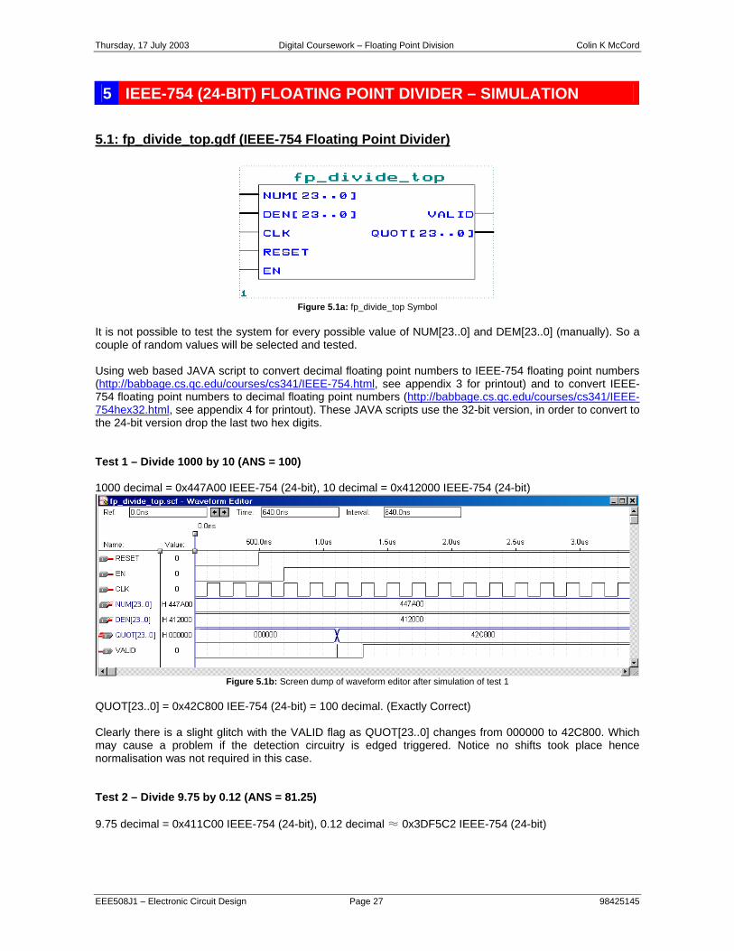
5 IEEE-754 (24-BIT) FLOATING POINT DIVIDER – SIMULATION 5.1: fp_divide_top.gdf (IEEE-754 Floating Point Divider)
Figure 5.1a: fp_divide_top Symbol
It is not possible to test the system for every possible value of NUM[23..0] and DEM[23..0] (manually). So a couple of random values will be selected and tested. Using web based JAVA script to convert decimal floating point numbers to IEEE-754 floating point numbers (http://babbage.cs.qc.edu/courses/cs341/IEEE-754.html, see appendix 3 for printout) and to convert IEEE-754 floating point numbers to decimal floating point numbers (http://babbage.cs.qc.edu/courses/cs341/IEEE-754hex32.html, see appendix 4 for printout). These JAVA scripts use the 32-bit version, in order to convert to the 24-bit version drop the last two hex digits. Test 1 – Divide 1000 by 10 (ANS = 100) 1000 decimal = 0x447A00 IEEE-754 (24-bit), 10 decimal = 0x412000 IEEE-754 (24-bit)
Figure 5.1b: Screen dump of waveform editor after simulation of test 1
QUOT[23..0] = 0x42C800 IEE-754 (24-bit) = 100 decimal. (Exactly Correct) Clearly there is a slight glitch with the VALID flag as QUOT[23..0] changes from 000000 to 42C800. Which may cause a problem if the detection circuitry is edged triggered. Notice no shifts took place hence normalisation was not required in this case. Test 2 – Divide 9.75 by 0.12 (ANS = 81.25) 9.75 decimal = 0x411C00 IEEE-754 (24-bit), 0.12 decimal ≈ 0x3DF5C2 IEEE-754 (24-bit)

Thursday, 17 July 2003 Digital Coursework – Floating Point Division Colin K McCord
EEE508J1 – Electronic Circuit Design Page 28 98425145
Figure 5.1c: Screen dump of waveform editor after simulation of test 2
QUOT[23..0] = 0x42A280 IEE-754 (24-bit) = 81.25 decimal. (Exactly Correct) Clearly this small glitch with the VALID flag has recurred. Notice that the result had to be normalised, by shifting one place to the left and decrementing the exponent (e.g. 0x435140 before normalisation). Test 3 – Divide 2.53 by 5.31 (ANS = 0.4764951) 2.53 decimal ≈ 0x4020A3 IEEE-754 (24-bit), 5.31 decimal ≈ 0x40A9EB IEEE-754 (24-bit)
Figure 5.1d: Screen dump of waveform editor after simulation of test 3
QUOT[23..0] = 0x3EF204 IEE-754 (24-bit) = 0.47268 decimal. (Correct to two decimal places) Test 4 – Divide -7.29 by 1.26 (ANS = -5.785714286) -7.29 decimal ≈ 0xC0E947 IEEE-754 (24-bit), 1.26 decimal ≈ 0x3FA147 IEEE-754 (24-bit) QUOT[23..0] = 0xC0B924 IEE-754 (24-bit) = -5.78564 decimal. (Correct to three decimal places)

Thursday, 17 July 2003 Digital Coursework – Floating Point Division Colin K McCord
EEE508J1 – Electronic Circuit Design Page 29 98425145
Figure 5.1e: Screen dump of waveform editor after simulation of test 4
Test 5 – Divide 1.2 x 1026 by 9.2 x 1021 (ANS = 1.304347826 x 10⁴) 1.2e26 decimal ≈ 0x6AC685 IEEE-754 (24-bit), 9.2e21 decimal ≈ 0x63F95D IEEE-754 (24-bit)
Figure 5.1f: Screen dump of waveform editor after simulation of test 5
QUOT[23..0] = 0x464BCC IEE-754 (24-bit) = 1.3043 x 10⁴ decimal. (Correct to four decimal places) Tests 6 to 10
Test Num DEC Num IEEE Den DEC Den IEEE Quot IEEE Quot DEC 6 32 0x420000 32e-15 0x29101D 0x586360 1.0000e15 7 1 0x3F8000 -1 0xBF8000 0xBF8000 -1 8 -10 0xC12000 -250 0xC37A00 0x3D23D6 3.9999e-2 9 0.1234 0x3DFCB9 0.4321 0x3EDD3C 0x3E9237 2.8558e-1 10 100e10 0x5368D4 100e-10 0x322BCC 0x60AD78 9.9998e19
Figure 5.1g: Result table for tests 6 to 10

Thursday, 17 July 2003 Digital Coursework – Floating Point Division Colin K McCord
EEE508J1 – Electronic Circuit Design Page 30 98425145
5.2: from_ieee.gdf (Convert From IEEE)
Figure 5.2a: from_ieee Symbol
Test 1 – Convert IEEE-754 (Figure 5.2b) into its Key Components 23 22 21 20 19 18 17 16 15 14 13 12 11 10 9 8 7 6 5 4 3 2 1 0 0 1 1 0 0 1 1 1 1 1 0 1 1 0 0 0 1 1 1 1 1 1 0 1 S Exponent Mantissa
Figure 5.2b: Test IEEE Number 1
Figure 5.2c: Screen dump of waveform editor after simulation of test 1
SIGN = 0, E[7..0] = 11001111 and M[14..0] = 101100011111101. Test 2 – Convert IEEE-754 (Figure 5.2d) into its Key Components 23 22 21 20 19 18 17 16 15 14 13 12 11 10 9 8 7 6 5 4 3 2 1 0 1 0 0 0 0 1 1 1 1 1 0 1 0 1 1 0 1 1 0 0 1 1 0 1 S Exponent Mantissa
Figure 5.2d: Test IEEE Number 2
Figure 5.2e: Screen dump of waveform editor after simulation of test 2
SIGN = 1, E[7..0] = 00001111, M[14..0] = 101011011001101
Thursday, 17 July 2003 Digital Coursework – Floating Point Division Colin K McCord
EEE508J1 – Electronic Circuit Design Page 31 98425145
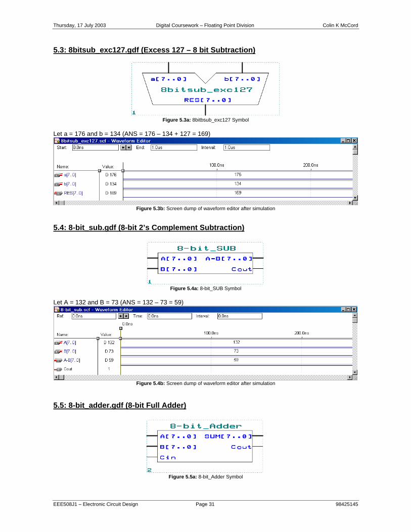
5.3: 8bitsub_exc127.gdf (Excess 127 – 8 bit Subtraction)
Figure 5.3a: 8bitbsub_exc127 Symbol
Let a = 176 and b = 134 (ANS = 176 – 134 + 127 = 169)
Figure 5.3b: Screen dump of waveform editor after simulation
5.4: 8-bit_sub.gdf (8-bit 2’s Complement Subtraction)
Figure 5.4a: 8-bit_SUB Symbol
Let A = 132 and B = 73 (ANS = 132 – 73 = 59)
Figure 5.4b: Screen dump of waveform editor after simulation
5.5: 8-bit_adder.gdf (8-bit Full Adder)
Figure 5.5a: 8-bit_Adder Symbol
Thursday, 17 July 2003 Digital Coursework – Floating Point Division Colin K McCord
EEE508J1 – Electronic Circuit Design Page 32 98425145
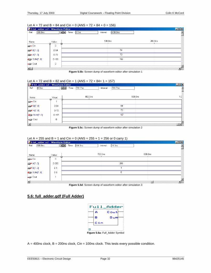
Let A = 72 and B = 84 and Cin = 0 (ANS = 72 + 84 + 0 = 156)
Figure 5.5b: Screen dump of waveform editor after simulation 1
Let A = 72 and B = 82 and Cin = 1 (ANS = 72 + 84+ 1 = 157)
Figure 5.5c: Screen dump of waveform editor after simulation 2
Let A = 255 and B = 1 and Cin = 0 (ANS = 255 + 1 = 256 or 0 carry 1)
Figure 5.5d: Screen dump of waveform editor after simulation 3
5.6: full_adder.gdf (Full Adder)
Figure 5.6a: Full_Adder Symbol
A = 400ns clock, B = 200ns clock, Cin = 100ns clock. This tests every possible condition.

Thursday, 17 July 2003 Digital Coursework – Floating Point Division Colin K McCord
EEE508J1 – Electronic Circuit Design Page 33 98425145
Figure 5.6b: Screen dump of waveform editor after simulation
Compare figure 5.6b with the truth table (Figure 4.6b) for the full adder; it is clear that their identical. Notice there is a slight propagation delay for the output to reflect the change of input. 5.7: int_divide.gdf (Integer Divider)
Figure 5.7a: int_divide Symbol
Recall that NUM[14..0] is convert to 32-bits and ‘1’ is hardwired to bit 31, Also DEN[14..0] is extend to 16-bits by hardwiring a ‘1’ to its MSB. Recall that the reason for this is to reduce rounding errors. Let NUM = 111 1111 1111 1111 and DEN = 000 0000 0000 0000.
Figure 5.7b: Screen dump of waveform editor after simulation 1
NUM[14..0] = 1111111 11111111 = 0xFFFF = 65535 N[31..0] = 11111111 11111111 00000000 00000000 = 0xFFFF0000 = 4294901760 DEN[14..0] = 0000000 00000000 = 0x0000 = 0 D[15..0] = 10000000 00000000 = 0x8000 = 32768 Q[31..0] = 00000000 00000000 11111111 11111111 = 0x0000FFFF = 65535 QUOT[15..0]= 11111111 11111111 = 0xFFFF = 65535 Using calculator 4294901760 / 32768 = 131070 or 0x1FFFE or 1 11111111 11111110 (QUOT = 0xFFFF, recall that QUOT uses bits 16 to 1 of Q). .

Thursday, 17 July 2003 Digital Coursework – Floating Point Division Colin K McCord
EEE508J1 – Electronic Circuit Design Page 34 98425145
Let NUM = 111 0000 1111 1111 and DEN = 000 0000 1111 0000.
Figure 5.7c: Screen dump of waveform editor after simulation 2
NUM[14..0] = 1110000 11111111 = 0x70FF = 28927 N[31..0] = 11110000 11111111 00000000 00000000 = 0xF0FF0000 = 4043243520 DEN[14..0] = 0000000 11110000 = 0x0078 = 120 D[15..0] = 10000000 11110000 = 0x80F0 = 33008 Q[31..0] = 00000000 00000000 11101111 00111110 = 0x0000EF3E = 61246 QUOT[15..0]= 11101111 00111110 = 0xEF3E = 61246 Using calculator 4043243520 / 33008 = 122492.84 or 0x1DE7C or 1 11011110 01111100 (QUOT = 0xEF7C = 61308, rounding errors are present). 5.8: normalize.gdf (Normalise Mantissa and Exponent)
Figure 5.8a: normalize Symbol
The propose of this block is to normalise the mantissa and exponent, e.g. shift mantissa left and dec exponent until mantissa MSB is ‘1’. Let M[15..0] = 0011011000000111 and E[7..0] = 100
Figure 5.8b: Screen dump of waveform editor after simulation 1

Thursday, 17 July 2003 Digital Coursework – Floating Point Division Colin K McCord
EEE508J1 – Electronic Circuit Design Page 35 98425145
MS[15..0] in figure 5.8a shows the output of the 16-bit shift register, clearly M[15..0] is loaded into this shift register and shifted two places to the left. Notice that the MSB of MS[15..0] is not include in MO[14..0] (IEEE-754 states that there must always be a hidden MSB ‘1’). Also notice that E[7..0] is DEC on every shift. Let M[15..0] = 1111011000000111 and E[7..0] = 100
Figure 5.8c: Screen dump of waveform editor after simulation 2
Let M[15..0] = 0000000000000001 and E[7..0] = 100
Figure 5.8d: Screen dump of waveform editor after simulation 3
Let M[15..0] = 0000000000000000 and E[7..0] = 100
Figure 5.8e: Screen dump of waveform editor after simulation 4

Thursday, 17 July 2003 Digital Coursework – Floating Point Division Colin K McCord
EEE508J1 – Electronic Circuit Design Page 36 98425145
5.9: 4counter.gdf (4-bit Synchronous Binary Up Counter)
Figure 5.9a: 4counter Symbol
Figure 5.9b: Screen dump of waveform editor after simulation
Counts from 0 – 15 – 0, notice when ENABLE went LOW the count paused at 9 until ENABLE went HIGH. 5.10: 16-bit_shiftreg.gdf (16-bit Configurable Shift Left Register)
Figure 5.10a: 16-bit_shiftreg Symbol
Figure 5.10b: Screen dump of waveform editor after simulation

Thursday, 17 July 2003 Digital Coursework – Floating Point Division Colin K McCord
EEE508J1 – Electronic Circuit Design Page 37 98425145
5.11: to_ieee.gdf (Convert To IEEE)
Figure 5.11a: to_ieee Symbol
Test 1 Sign = 0 Exponent = 11001111 Mantissa = 101100011111101
Figure 5.11b: Screen dump of waveform editor after simulation of test 1
23 22 21 20 19 18 17 16 15 14 13 12 11 10 9 8 7 6 5 4 3 2 1 0 0 1 1 0 0 1 1 1 1 1 0 1 1 0 0 0 1 1 1 1 1 1 0 1 S Exponent Mantissa
Figure 5.11c: IEEE[23..0] Test 2 Sign = 1 Exponent = 00001111 Mantissa = 101011011001101
Figure 5.11d: Screen dump of waveform editor after simulation of test 2
23 22 21 20 19 18 17 16 15 14 13 12 11 10 9 8 7 6 5 4 3 2 1 0 1 0 0 0 0 1 1 1 1 1 0 1 0 1 1 0 1 1 0 0 1 1 0 1 S Exponent Mantissa
Figure 5.2e: IEEE[23..0]

Thursday, 17 July 2003 Digital Coursework – Floating Point Division Colin K McCord
EEE508J1 – Electronic Circuit Design Page 38 98425145
6 CONCLUSIONS The purpose of this assignment was to design a floating point divider unit, that complies with the IEEE-754 standard (24-bit version) using the Altera Max2Plus package. Clearly this objective has been achieved successfully, as it has been proven using simulation the design works, although further development is required as there are limitations and flaws in the current design. Evidently the IEEE-754 standard for representing floating point numbers is not perfect, it is important to be aware rounding error’s occur frequently. Although the 32-bit (single precision) and 64-bit (double precision) IEEE-754 formats, will produce more accurate decimal representations than the 24-bit version, but even these, will frequently contain rounding errors. Recall that 0.085 cannot be represented accurately using IEEE-754, 8.4999e-2 (0x3DAE14) is the best for 24-bit IEEE and 8.5000001e-2 (0x3DAE147B) is the best for 32-bit IEEE. Clearly ASM (Algorithmic State Machine) charts are useful to the digital design engineer, as they represent the operation of a digital system and are easier to understand than state diagrams. Another advantage of the ASM method is that the chart can be converted into several equivalent forms, each form leads directly to a hardware realisation. It is clear that an ASM chart contains only three elements, ‘state box’, ‘decision box’ and ‘conditional output box’, unlike flowcharts which have many more elements, which can become confusing on what box should be use. The ASM chart and the ‘one hot’ method can be used to design the control logic to control the system, easily and quickly. This method was not used in the design of the floating point divider unit as it would produce over 10 states (notice the finished design only has 4 states) and the control logic would be must more complex, although a simplified ASM chart was drawn to help explain how the system works (see figure 4.8b). The ASM method is more useful for more complex designs (e.g. complete CPU). Intel is one of the worlds leading microprocessor designers / manufactures, the original Pentium processor had a bug with the floating point divider. Even through they ran exhaustive functional simulations, these simulations were unable to detect the bug and the processor was released onto the market. Clearly if Intel FPU had a flaw, it is unlikely that this 24-bit floating point divider is flawless. The main reason why Intel’s exhaustive functional simulations failed to find the bug was because the same person that designed the FPU also wrote the RTL simulation script (e.g. the RTL code also contained the bug). Evidently to divide two floating point numbers, subtract the exponents and divide the mantissas. Clearly 127 must be added to the result of the subtraction as IEEE-754 exponents are 127-biased and if two of these numbers are subtracted the bias is removed, which must be restored. Originally it was thought that a 16-bit integer divider could be used to divide the mantissas, but the rounding errors were too large and the correct result could not be obtained. Clearly conversion of the NUM mantissa to 32-bits reduces rounding errors, the result is now almost as actuate as that can be represented in the IEEE-754 24-bit. Using a 17-bit shift register instead of using a 16-bit, would have slightly improved the situation (actuate as that can be represented in the IEEE-754 24-bit), but it was decide to keep the design simple and easy to describe, hence the LSB was dropped and a 16-bit bit shift register was used. Clearly an XOR gate takes care of the Sign bits, e.g. if either NUM or DEN sign = 1 the QUOT sign = 1, if NUM = 1 and DEN = 1 the QUOT = 0, and if DEN = 0 and DEN = 0 the QUOT = 0. IEEE-754 states that there is a hidden MSB bit in the mantissas, obviously this hidden MSB bit must be included in the divide calculation and removed during the normalisation process. Originally this was forgotten, during simulations it was discovered that the result was not correct. After a while, it was discovered that these hidden MSB bits must be included in the calculation and sure enough one they were include and the MSB bit was removed during the normalisation process the correct results were being simulated. Clearly simulation is extremely powerful and useful to the design engineer, e.g. in this case, simulation was able to quickly show that something was wrong with the design, and allowed the engineer to quickly rectify the problem. The design was partitioned into many functional blocks; each block did one task that was easily described. Evidently this partitioned method of design made the design and testing of the system extremely easy. Screen dumps of the design of each functional block were included in this report along with an English

Thursday, 17 July 2003 Digital Coursework – Floating Point Division Colin K McCord
EEE508J1 – Electronic Circuit Design Page 39 98425145
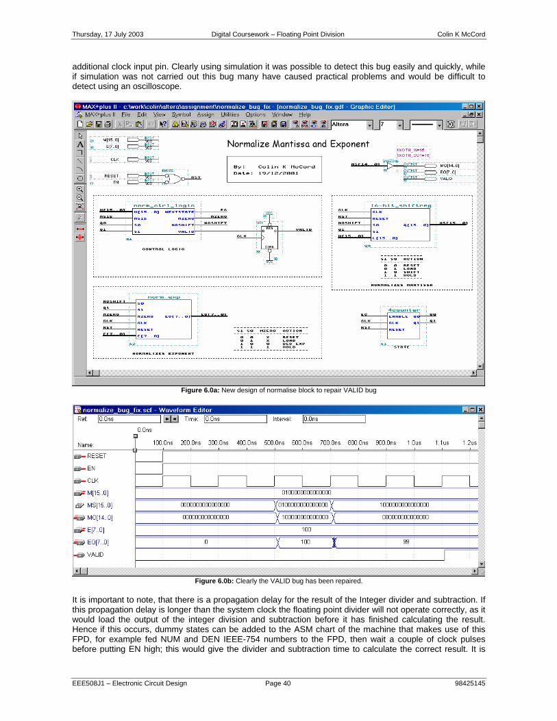
description on how the each blocked operated. Clearly each block carried out simple tasks, which are easily understood and described. Notice comments are also included on the design files. Notice block ‘norm_ctrl_logic’ section 1 (Figure 4.10b) detects if the mantissa is zero and in the shifting state, MZERO becomes ‘1’. This forces the state counter to move to the holding state; hence it is not possible to be stuck in the shifting state. Clearly this logic circuitry is not required; originally it was forgotten that MSB ‘1’s are included in the integer divider, hence in that case, it was possible that the mantissa may equal zero and this circuitry was required to breakout of the shifting state. This circuitry can be safely remove, but because it’s not doing any harm and because of the lack of time, it was decide to leave it. Clearly removing this circuitry will simplify the control logic. Notice block ‘norm_ctrl_logic’ section 2 (Figure 4.10c) detects if in the shifting state and MS15 is ‘1’, the logic output NOSHIFT is used to make sure that during the normalising process the shift register does not shift one place too many. Originally this circuitry was not included and during simulation of this functional block it was discovered that this bug existed, and the NOSHIFT circuitry was designed to fix this problem. Clearly all this happen before it was understood that MSB ‘1’s were included in the integer division and the MSB ‘1’ of QUOT had to be removed during the normalising process. Clearly the original bug of shifting one to many is a good method of getting rid of the MSB bit; the only downside of this is that one additional shift will always take place hence it would be slower. It was decide to leave it as it was and not include the MSB bit in the final result. Evidently the circuitry (figure 4.10c) can be removed, as long as bits 16 to 1 are used as the result and not bits 15 to 0. This simplifies the control logic, but increases the time it takes to normalise the result by 1 clock pulse. The state controller (figure 4.10e) uses a four – line multiplexer to control the state counter. It is clear that this offers an extremely simple solution than if it was design using the ‘one hot’ method. The current state is fed into the select line of the multiplexer, DO & D1 is connected to VCC, D2 is connected to MS15, and D3 is connected to GND. It is extremely clear what is happening, if state = 00 (reset state) line D0 is selected hence the counter is enabled and moves to state 01 (load state) on the next clock pulse. If state = 01 (load state) line D1 is selected hence the counter is enabled and moves to state 10 (shifting state) on the next clock pulse. Clearly if state = 10 (shifting state) line D2 is selected and the counter will be disabled until MSB15 = ‘1’ then move to state 11 on the next clock pulse. If state = 11 (holding state) line D3 is selected and the counter is disabled and stays in the hold state until it is reset (e.g. RESET, or EN goes LOW). Obviously this is a unique and easy solution. The entire system was simulated and proven to work, although obviously it’s not possible to test every possible value of NUM[23..0] and DEN[23..0] manually. Clearly converting decimal numbers to IEEE-754 numbers is a slow and boring process and the revise is also as tedious, chapter 2 demonstrates how to carryout these conversions manually. During the simulation process of the entire system, web based JAVA scripts were used to do the conversions automatically (see appendixes 3 and 4) these allow for the system to be tested quickly and easily. 10 Tests are documented in this report, but in reality many more were carried out. Indisputably the system works, there are rounding errors for some situations but that is expected as the 24-bit IEEE-754 is only accurate to a couple of significant digits. If more accurate results are required IEEE-754 32-bit and 64-bit should be considered, it is easy to adapt this design to suit. For example to modify the design of 32-bit IEEE-754, use a 48-bit by 24-bit integer divider, a 24-bit shift register, along with some minor changes (e.g. instead of M15 connected to control logic use M23). Clearly the design works and is extremely flexible. Simulation results show that there is a small glitch with the VALID flag, this glitch was unexpected and may cause problems. Figure 4.10d shows the circuitry used to activate the VALID flag, notices that S0 and S1 is connected to an AND gate, it is assumed that if S0 = 1 and S1 = 1 (holding state) the normalising process is finished and the data is valid. Notice that the glitch occurs as state moves from the reset state (00) to the load state (01), for some reason briefly state move to 11 first then 01, but because the shift register and normalise exponent blocks are synchronised to clock it does not affect there results. Hence the solution to this problem is to synchronise the VALID flag with the clock, e.g. fed the output of the AND gate into a D-type flip-flop which feds the VALID output, hence the VALID flag will only change on a clock pulse. This solution has been implemented and proven via simulation to work see figures 6.0a and 6.0b. Notice the flip-flop has been placed outside of the control logic block, the reason for this is the control logic does not have a clock input and for speed (laziness) the flip-flop was connected outside the control logic, obviously now it is clear that this repairs the bug it makes since to include the flip-flop in the control logic and add an
Thursday, 17 July 2003 Digital Coursework – Floating Point Division Colin K McCord
EEE508J1 – Electronic Circuit Design Page 40 98425145
additional clock input pin. Clearly using simulation it was possible to detect this bug easily and quickly, while if simulation was not carried out this bug many have caused practical problems and would be difficult to detect using an oscilloscope.
Figure 6.0a: New design of normalise block to repair VALID bug
Figure 6.0b: Clearly the VALID bug has been repaired.
It is important to note, that there is a propagation delay for the result of the Integer divider and subtraction. If this propagation delay is longer than the system clock the floating point divider will not operate correctly, as it would load the output of the integer division and subtraction before it has finished calculating the result. Hence if this occurs, dummy states can be added to the ASM chart of the machine that makes use of this FPD, for example fed NUM and DEN IEEE-754 numbers to the FPD, then wait a couple of clock pulses before putting EN high; this would give the divider and subtraction time to calculate the correct result. It is

Thursday, 17 July 2003 Digital Coursework – Floating Point Division Colin K McCord
EEE508J1 – Electronic Circuit Design Page 41 98425145
possible to calculate the propagation delay of the divider and subtraction using simulation, and then calculate the maximum system clock that can be used, before dummy states are required. Clearly the designed floating point divider calculates its answer extremely quickly, the reason for this is that the mantissa and exponent are normalised simultaneously using the system clock to synchronise the process. Obviously the fastest possible calculation time occurs after 4 clock-pulses when no normalising is required and the slowest is 5 clock-pulses because MSB ‘1’ are inserted into the integer divider the maximum number of shifts required is 1 (e.g. 10000000000000000000000000000000 divided by 1111111111111111 = 0100000000000000). Therefore this floating point divider produces a result after 4 to 5 clock pulses, extremely efficient, seen nothing that can beat it. Clearly a floating point divider using the Altera Max2Plus software package was successfully designed, analyses and proved. The system was successfully fitted into Altera’s EPF10K20TC144-3; Appendix 2 shows the pin layout. The system is as actuate as, possible with the IEE-754 24-bit version, and the performance is second to none. Although because a truly combinational solution was used for the integer divider a large percentage of the 10k20 chip is used up, which does not leave much room for anything else (a larger chip could be used e.g. 10k50). A pipeline integer divider would use less resources but the performance of the calculation would be much slower.

Thursday, 17 July 2003 Digital Coursework – Floating Point Division Colin K McCord
EEE508J1 – Electronic Circuit Design Page 42 98425145
A1 HIERARCHY CHART FOR FP_DIVIDE_TOP.GDF

Thursday, 17 July 2003 Digital Coursework – Floating Point Division Colin K McCord
EEE508J1 – Electronic Circuit Design Page 43 98425145
A2 Fp_divide_top.pin -- Copyright (C) 1988-2001 Altera Corporation -- Any megafunction design, and related net list (encrypted or decrypted), -- support information, device programming or simulation file, and any other -- associated documentation or information provided by Altera or a partner -- under Altera's Megafunction Partnership Program may be used only to -- program PLD devices (but not masked PLD devices) from Altera. Any other -- use of such megafunction design, net list, support information, device -- programming or simulation file, or any other related documentation or -- information is prohibited for any other purpose, including, but not -- limited to modification, reverse engineering, de-compiling, or use with -- any other silicon devices, unless such use is explicitly licensed under -- a separate agreement with Altera or a megafunction partner. Title to -- the intellectual property, including patents, copyrights, trademarks, -- trade secrets, or maskworks, embodied in any such megafunction design, -- net list, support information, device programming or simulation file, or -- any other related documentation or information provided by Altera or a -- megafunction partner, remains with Altera, the megafunction partner, or -- their respective licensors. No other licenses, including any licenses -- needed under any third party's intellectual property, are provided herein. N.C. = No Connect. This pin has no internal connection to the device. VCCINT = Dedicated power pin, which MUST be connected to VCC (5.0 volts). VCCIO = Dedicated power pin, which MUST be connected to VCC (5.0 volts). GNDINT = Dedicated ground pin or unused dedicated input, which MUST be connected to GND. GNDIO = Dedicated ground pin, which MUST be connected to GND. RESERVED = Unused I/O pin, which MUST be left unconnected. ---------------------------------------------------------------------------- CHIP "fp_divide_top" ASSIGNED TO AN EPF10K20TC144-3 TCK : 1 CONF_DONE : 2 nCEO : 3 TDO : 4 VCCIO : 5 VCCINT : 6 RESERVED : 7 NUM23 : 8 NUM22 : 9 DEN20 : 10 QUOT8 : 11 QUOT10 : 12 QUOT11 : 13 QUOT9 : 14 GNDIO : 15 GNDINT : 16 NUM6 : 17 NUM8 : 18 RESERVED : 19 RESERVED : 20 QUOT15 : 21 NUM11 : 22 RESERVED : 23 VCCIO : 24 VCCINT : 25 NUM2 : 26 RESERVED : 27 NUM3 : 28 NUM1 : 29 QUOT3 : 30 QUOT14 : 31 QUOT2 : 32 QUOT1 : 33 TMS : 34 nSTATUS : 35 DEN15 : 36 EN : 37 QUOT20 : 38 RESET : 39 GNDIO : 40 QUOT17 : 41

Thursday, 17 July 2003 Digital Coursework – Floating Point Division Colin K McCord
EEE508J1 – Electronic Circuit Design Page 44 98425145
QUOT16 : 42 QUOT7 : 43 DEN17 : 44 VCCIO : 45 DEN0 : 46 QUOT4 : 47 DEN16 : 48 DEN3 : 49 GNDIO : 50 NUM16 : 51 VCCINT : 52 VCCINT : 53 DEN2 : 54 CLK : 55 DEN8 : 56 GNDINT : 57 GNDINT : 58 RESERVED : 59 RESERVED : 60 VCCIO : 61 RESERVED : 62 RESERVED : 63 RESERVED : 64 DEN5 : 65 GNDIO : 66 RESERVED : 67 DEN14 : 68 RESERVED : 69 RESERVED : 70 VCCIO : 71 RESERVED : 72 RESERVED : 73 nCONFIG : 74 VCCINT : 75 MSEL1 : 76 MSEL0 : 77 NUM10 : 78 QUOT0 : 79 QUOT6 : 80 VALID : 81 NUM0 : 82 DEN6 : 83 GNDINT : 84 GNDIO : 85 NUM4 : 86 NUM5 : 87 DEN10 : 88 NUM14 : 89 NUM12 : 90 NUM9 : 91 RESERVED : 92 VCCINT : 93 VCCIO : 94 NUM19 : 95 DEN18 : 96 DEN22 : 97 DEN21 : 98 NUM21 : 99 RESERVED : 100 NUM7 : 101 DEN23 : 102 GNDINT : 103 GNDIO : 104 TDI : 105 nCE : 106 DCLK : 107 DATA0 : 108 RESERVED : 109 RESERVED : 110 DEN9 : 111 RESERVED : 112 DEN7 : 113 RESERVED : 114 VCCIO : 115 RESERVED : 116 DEN13 : 117 NUM13 : 118

Thursday, 17 July 2003 Digital Coursework – Floating Point Division Colin K McCord
EEE508J1 – Electronic Circuit Design Page 45 98425145
RESERVED : 119 RESERVED : 120 RESERVED : 121 NUM18 : 122 VCCINT : 123 DEN11 : 124 DEN12 : 125 DEN4 : 126 GNDINT : 127 DEN1 : 128 GNDIO : 129 NUM17 : 130 QUOT12 : 131 DEN19 : 132 NUM20 : 133 VCCIO : 134 QUOT18 : 135 QUOT19 : 136 QUOT5 : 137 QUOT22 : 138 GNDIO : 139 QUOT21 : 140 QUOT13 : 141 NUM15 : 142 RESERVED : 143 QUOT23 : 144

Thursday, 17 July 2003 Digital Coursework – Floating Point Division Colin K McCord
EEE508J1 – Electronic Circuit Design Page 46 98425145
A3 CONVERSION OF DECIMAL TO IEEE-754 – JAVA SCRIPT
Source: http://babbage.cs.qc.edu/courses/cs341/IEEE-754.html

Thursday, 17 July 2003 Digital Coursework – Floating Point Division Colin K McCord
EEE508J1 – Electronic Circuit Design Page 47 98425145
A4 CONVERSION OF IEEE-754 TO DECIMAL – JAVA SCRIPT
Source: http://babbage.cs.qc.edu/courses/cs341/IEEE-754hex32.html

Thursday, 17 July 2003 Digital Coursework – Floating Point Division Colin K McCord
EEE508J1 – Electronic Circuit Design Page 48 98425145
A5 FLOATING POINT PIPELINED DIVIDER – COMMERCIAL EXAMPLE

Thursday, 17 July 2003 Digital Coursework – Floating Point Division Colin K McCord
EEE508J1 – Electronic Circuit Design Page 49 98425145

Thursday, 17 July 2003 Digital Coursework – Floating Point Division Colin K McCord
EEE508J1 – Electronic Circuit Design Page 50 98425145
A6 CD ROM – CONTAINING DESIGN AND SIMULATION FILES
This CD ROM contains all the design and simulation files for the floating point divider. The web-based JAVA scripts shown in appendixes 3 and 4 are also included.
CD-ROM