Embed Size (px)
Citation preview
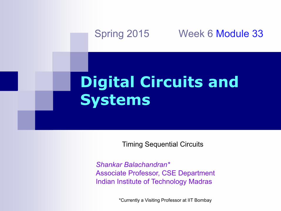
Shankar Balachandran*
Associate Professor, CSE Department
Indian Institute of Technology Madras
*Currently a Visiting Professor at IIT Bombay
Digital Circuits and Systems
Spring 2015 Week 6 Module 33
Timing Sequential Circuits

Analysis and Design of Sequential Logic Circuits 2
Sequential Circuit Timing
Once the functionality of a sequential network is designed,
its timing parameters must be determined. Timing problems
can be very subtle because timing parameters can vary with
device age and other operating conditions.

Analysis and Design of Sequential Logic Circuits 3
Global setup time (Tsu)
Global hold time (Th)
Maximum clock frequency
Clock skew.
These parameters are derived using the circuit (known) delays
described below.
tio – delay from input of IFL to output of OFL
tif – delay from circuit inputs of flip-flop inputs
tfo – delay from flip-flop outputs to circuit outputs
tff – delay from flip-flop outputs to flip-flop inputs
tc-q– clock to Q propagation delay of flip-flops
tsu – setup time of flip-flops
th – hold time of flip-flops
tc – clock delay; time required for clock to reach all flip-flops
Timing Parameters

Analysis and Design of Sequential Logic Circuits 4
X (at sequential circuit input)
Changes that occur at inputs can be delayed by as much as
maximum tif by the time they reach the flip-flop inputs. Hence,
we want to setup circuit inputs relative to clock edge appearing
at the flip-flops.
Similarly, hold time of the circuit inputs relative to the system
clock at the source is given by
max max minifu su cs t t tT
max min maxh if chT t t t
Global Setup and Hold Times
Tsu Th
th
tsu
CLK (at clock source) tc
CK (at FF clock input)
tif
tif
D (at FF input)

Analysis and Design of Sequential Logic Circuits 5
Maximum Clock Frequency
For an edge-triggered circuit: minimum clock period is,
Maximum Clock Frequency:
C Q ff sumax maxmax
clk t t tT
clk
clkT
f1
Comb.
logic
Λ
Qi Di
Qj Dj
CKi
CKj
tff
Λ
CLK
tsu
Tck (=Tclk)
CKi
Edge Triggering
tff
Dj
Qi
tC-Q

Analysis and Design of Sequential Logic Circuits 6
Timing Violations
The clock period (Tclk) has a lower bound of tff.max .
If the clock period is equal to (tff.max + tC-Q.max) then the
flip-flop state changes can violate setup times.
Remedy :
Use faster flip-flops (decrease tC-Q )
Use faster gates (decrease tff )
Use a slower clock (increase clock period, Tclk)
max maxmaxfC fl uc k Q st tT t

Analysis and Design of Sequential Logic Circuits 7
The previous discussion assumes that clock signals
arrive at all flip-flops simultaneously - this is not a good
assumption since it is not true in practice.
Because of different wire lengths over which the clock
signals travel and the load at the destination, there is a
slight difference in clock arrival times at different flip-flop
inputs.
Clock skew, tskew, is the difference in time between
triggering edges seen at different flip-flops. Clock skew
affects minimum Tclk.
Clock Skew

Analysis and Design of Sequential Logic Circuits 8
Therefore, for an edge-triggered circuit with clock skew,
Clock skew is a significant factor in determining the speed of high-
performance synchronous circuits. The larger the skew, the slower the circuit will operate.
max max max maxclk skew C Q ff suT t t t t
Max. Clock Frequency with Skew
tskew
Comb.
logic
Λ
Qi Di
Qj Dj
CKi
CKj
tff
Λ
CLK
tsu
Tck (=Tclk)
CKi tskew
CKj tC-Q
Qj tff
Di

Analysis and Design of Sequential Logic Circuits 10
For the circuit given below determine all the sequential
circuit timing parameters.
For a D flip-flop use: tsu = 2ns, th = 15ns and tC-Q = 20ns
For a NAND gate use: tp,max = 10ns and tp,min = 3ns
Timing Analysis Example

Analysis and Design of Sequential Logic Circuits 11
.
nstt
nstt
nstt
nstt
nstt
nstt
nandpc
nandpc
nandpff
nandpff
nandpif
nandpif
62
202
62
202
62
303
min,,min,
max,,max,
min,,min,
max,,max,
min,,min,
max,,max,
,max ,max ,min
,max ,min ,max
,max ,max ,max
,max
2 30 6 26
20 15 6 29
20 20 2 42
1/ 42 23.8
su su if c
h h if c
clk C Q ff su
clk
T t t t ns
T t t t ns
T t t t ns
f ns MHz
For a D flip-flop use: tsu = 2ns, th = 15ns, tC-Q = 20ns
For a NAND gate use: tp,max = 10ns, tp,min = 3ns

Analysis and Design of Sequential Logic Circuits 12
Sequential Systems Using Latches
Latches can be used to create sequential systems. However, since these
are level-triggered clocking must be done carefully – must ensure that state
changes only once per clock cycle.
Use narrow-width clock whose pulse width is less than the fastest possible path
through the combinational logic.
To guarantee correct next state, make sure that the clock period is longer than the
worst-case propagation delay through the combinational logic.
Comb.
logic Qi Di
Qj Dj
CKi
CKj
tff CLK
tw < tff.min+ tD-Q.min
> (tD-Q.max + tff.max+ tsu.max)
CLK

Analysis and Design of Sequential Logic Circuits 14
Clocking Frequency with Latches
Tclk
tskew
Comb.
logic Qi Di
Qj Dj
CKi
CKj
tff CLK
tsu
CKi
tD-Q
Q
j tff
Dj
tskew
CK
j
Di
max min max max maxclk skew w su D Q ff suT t t t t t t
tsu
tw

End of Week 6: Module 33
Thank You
Intro to State Machines 15