Embed Size (px)
Citation preview
Differential and Multistage Amplifiers
M2-3 DA & Multi-stage Amp, Sedra/Smith
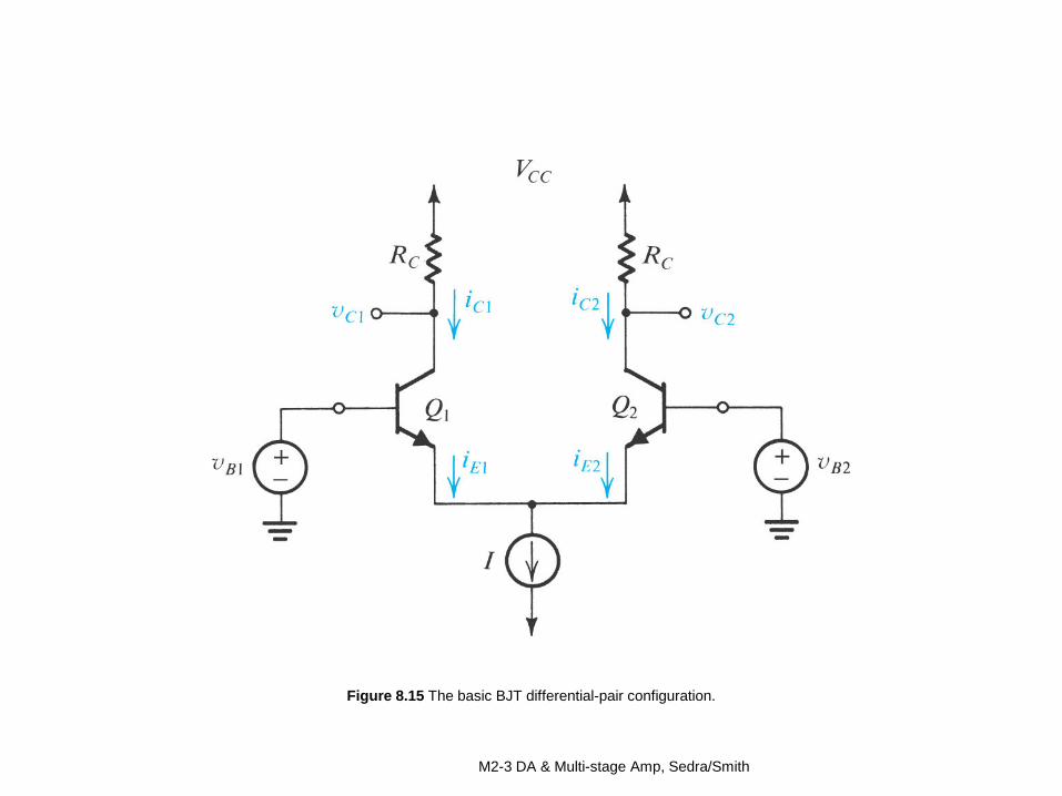
Figure 8.15 The basic BJT differential-pair configuration.
M2-3 DA & Multi-stage Amp, Sedra/Smith

M2-3 DA & Multi-stage Amp, Sedra/Smith

Figure E8.9
M2-3 DA & Multi-stage Amp, Sedra/Smith

M2-3 DA & Multi-stage Amp, Sedra/Smith

Figure 8.18 The transfer characteristics of the BJT differential pair (a) can be linearized (b) (i.e., the linear range of operation can be extended) by including resistances in the emitters.
M2-3 DA & Multi-stage Amp, Sedra/Smith

M2-3 DA & Multi-stage Amp, Sedra/Smith
M2-3 DA & Multi-stage Amp, Sedra/Smith
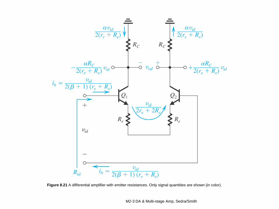
Figure 8.21 A differential amplifier with emitter resistances. Only signal quantities are shown (in color).
M2-3 DA & Multi-stage Amp, Sedra/Smith

Figure 8.22 Equivalence of the BJT differential amplifier in (a) to the two common-emitter amplifiers in (b). This equivalence applies only for differential input signals. Either of the two common-emitter amplifiers in (b) can be used to find the differential gain, differential input
resistance, frequency response, and so on, of the differential amplifier.
M2-3 DA & Multi-stage Amp, Sedra/Smith

Figure 8.23 The differential amplifier fed in a single-ended fashion.
M2-3 DA & Multi-stage Amp, Sedra/Smith
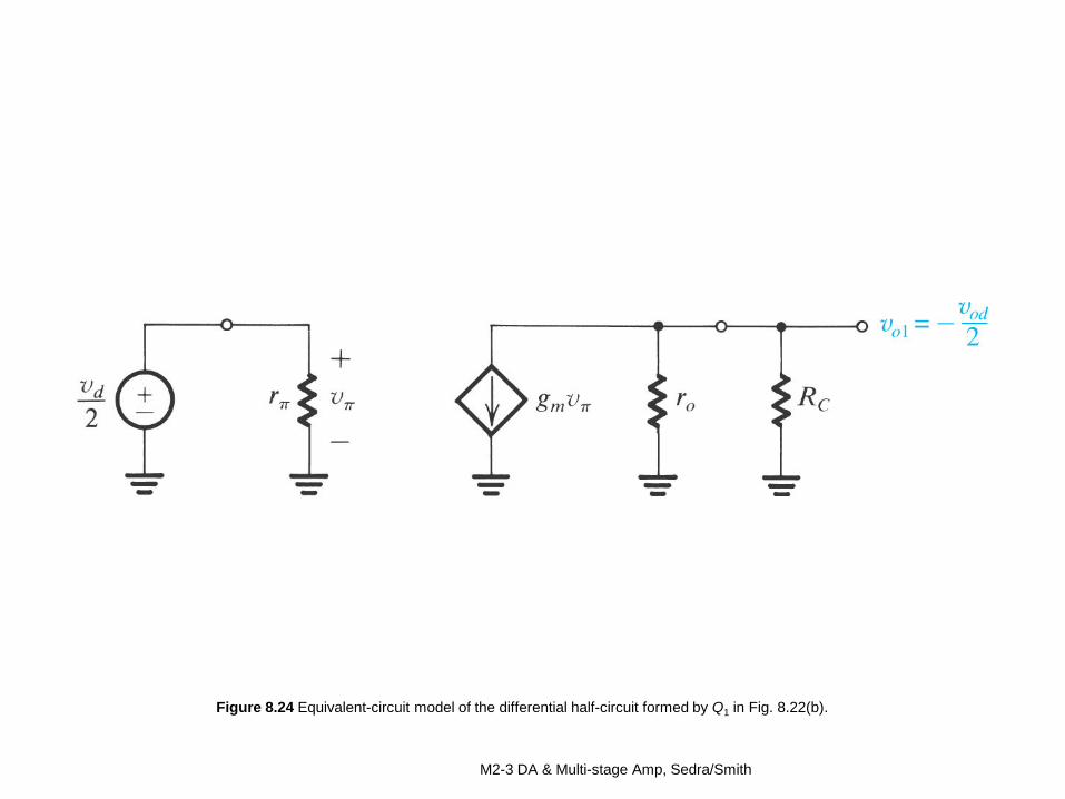
Figure 8.24 Equivalent-circuit model of the differential half-circuit formed by Q1 in Fig. 8.22(b).
M2-3 DA & Multi-stage Amp, Sedra/Smith

M2-3 DA & Multi-stage Amp, Sedra/Smith

Figure 8.26 (a) Definition of the input common-mode resistance Ricm . (b) The equivalent common-mode half-circuit.
M2-3 DA & Multi-stage Amp, Sedra/Smith

Figure 8.27 Circuit for Example 8.4.
M2-3 DA & Multi-stage Amp, Sedra/Smith
M2-3 DA & Multi-stage Amp, Sedra/Smith

Figure 8.30 A three-stage amplifier consisting of two differential-in, differential-out stages, A1 and A2, and a differential-in, single-ended-out stage A3.
M2-3 DA & Multi-stage Amp, Sedra/Smith

Figure 8.31 A simple but inefficient approach for differential to single-ended conversion.
M2-3 DA & Multi-stage Amp, Sedra/Smith
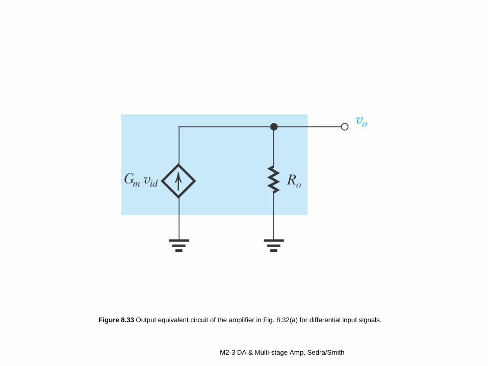
Figure 8.33 Output equivalent circuit of the amplifier in Fig. 8.32(a) for differential input signals.
M2-3 DA & Multi-stage Amp, Sedra/Smith
M2-3 DA & Multi-stage Amp, Sedra/Smith

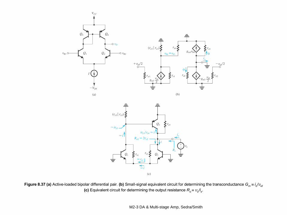
Figure 8.38 Analysis of the bipolar active-loaded differential amplifier to determine the common-mode gain.
M2-3 DA & Multi-stage Amp, Sedra/Smith
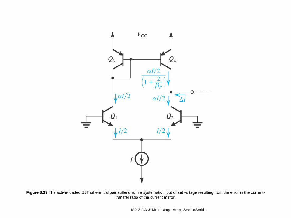
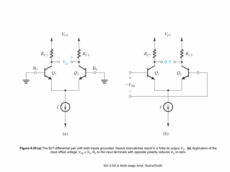
Figure 8.39 The active-loaded BJT differential pair suffers from a systematic input offset voltage resulting from the error in the current-transfer ratio of the current mirror.
M2-3 DA & Multi-stage Amp, Sedra/Smith
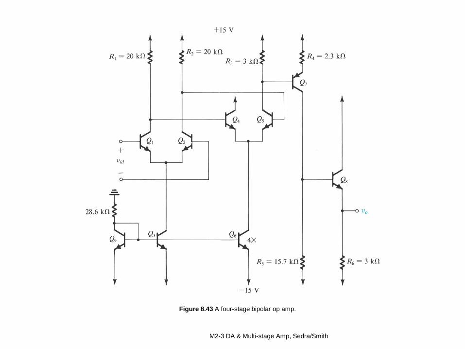
Figure 8.43 A four-stage bipolar op amp.
M2-3 DA & Multi-stage Amp, Sedra/Smith
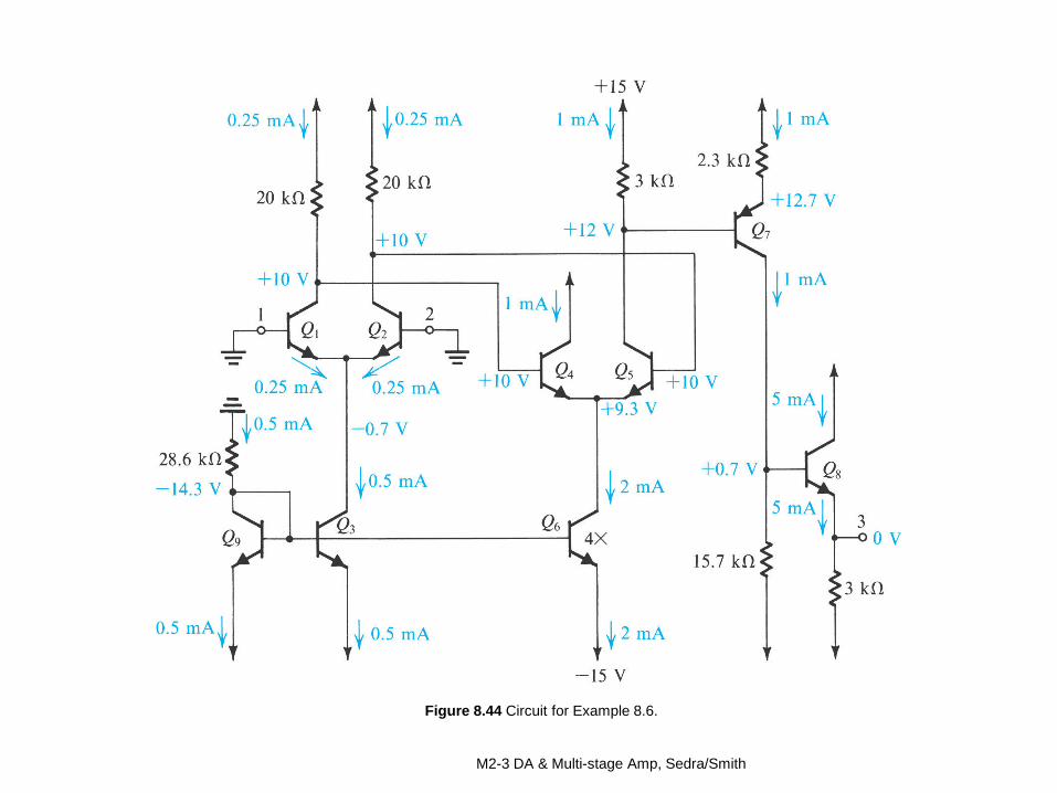
Figure 8.44 Circuit for Example 8.6.
M2-3 DA & Multi-stage Amp, Sedra/Smith

Figure 8.45 Equivalent circuit for calculating the gain of the input stage of the amplifier in Fig. 8.43.
M2-3 DA & Multi-stage Amp, Sedra/Smith
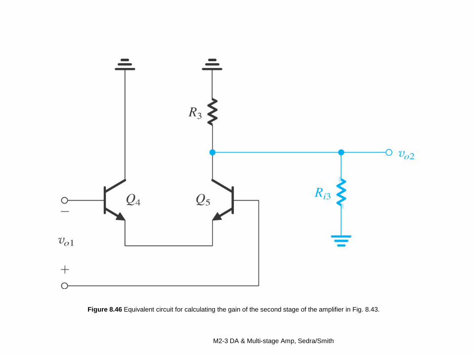
Figure 8.46 Equivalent circuit for calculating the gain of the second stage of the amplifier in Fig. 8.43.
M2-3 DA & Multi-stage Amp, Sedra/Smith

Figure 8.47 Equivalent circuit for evaluating the gain of the third stage in the amplifier circuit of Fig. 8.43.
M2-3 DA & Multi-stage Amp, Sedra/Smith
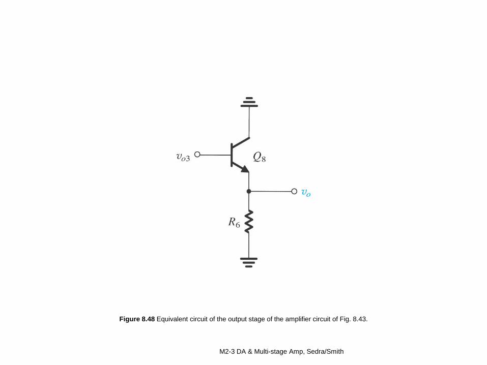
Figure 8.48 Equivalent circuit of the output stage of the amplifier circuit of Fig. 8.43.
M2-3 DA & Multi-stage Amp, Sedra/Smith

Figure 8.49 The circuit of the multistage amplifier of Fig. 8.43 prepared for small-signal analysis. Indicated are the signal currents throughout the amplifier and the input resistances of the four stages.
M2-3 DA & Multi-stage Amp, Sedra/Smith

Figure P8.54
M2-3 DA & Multi-stage Amp, Sedra/Smith
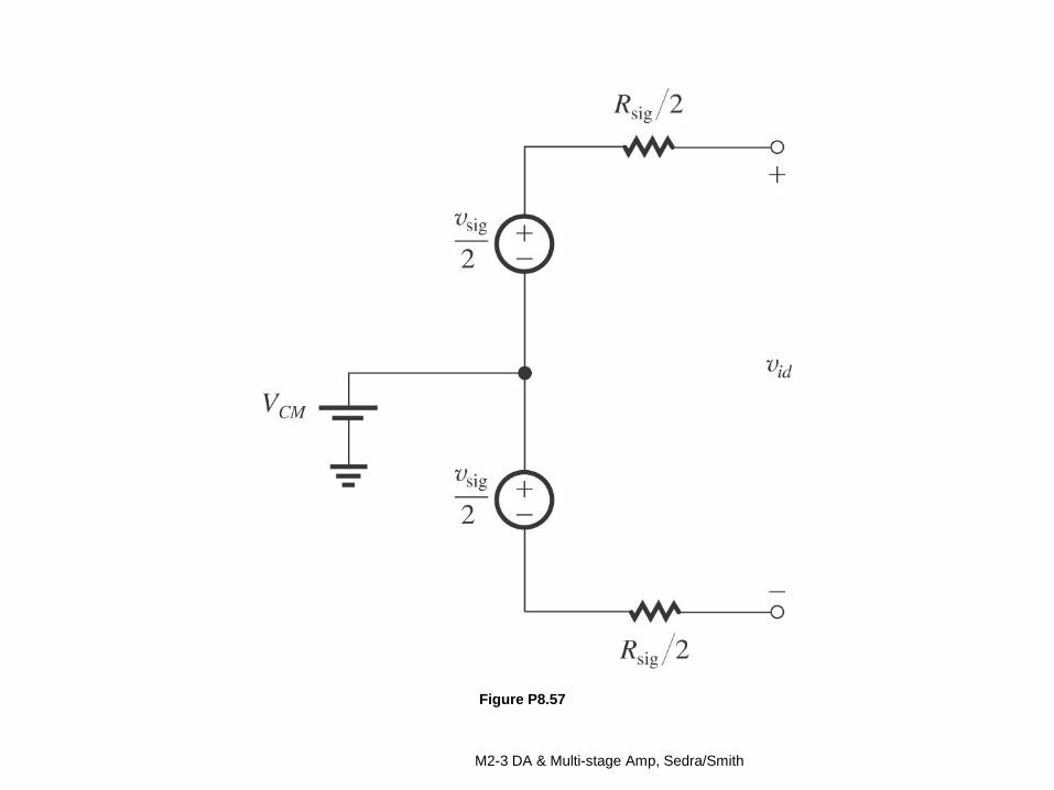
Figure P8.57
M2-3 DA & Multi-stage Amp, Sedra/Smith

Figure P8.59
M2-3 DA & Multi-stage Amp, Sedra/Smith
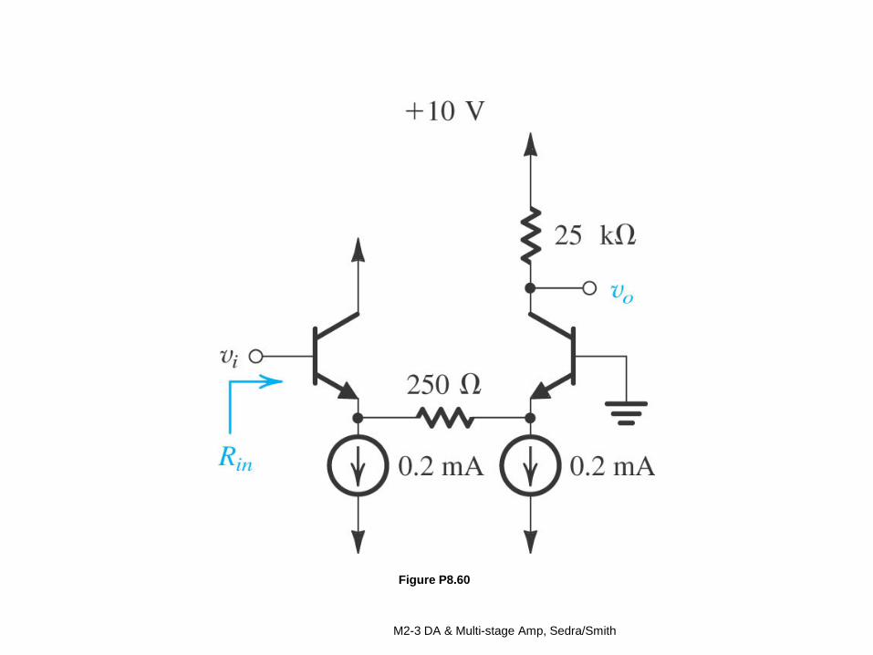
Figure P8.60
M2-3 DA & Multi-stage Amp, Sedra/Smith

Figure P8.61
M2-3 DA & Multi-stage Amp, Sedra/Smith

Figure P8.62
M2-3 DA & Multi-stage Amp, Sedra/Smith

Figure P8.63
M2-3 DA & Multi-stage Amp, Sedra/Smith
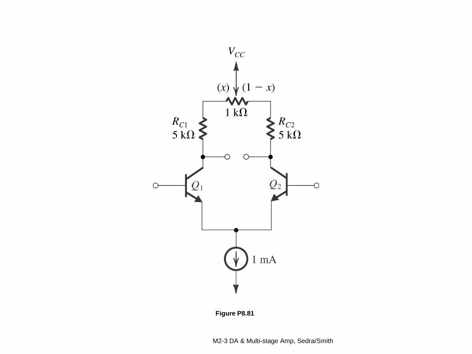
Figure P8.81
M2-3 DA & Multi-stage Amp, Sedra/Smith

Figure P8.98
M2-3 DA & Multi-stage Amp, Sedra/Smith
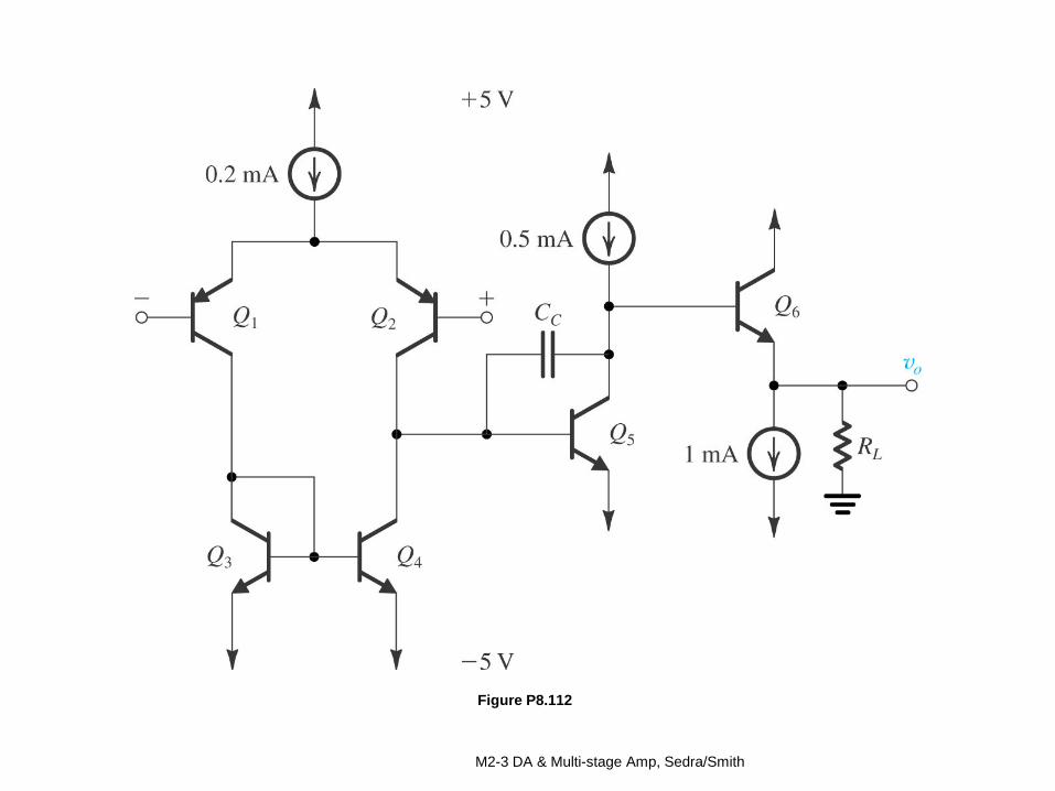
Figure P8.112
M2-3 DA & Multi-stage Amp, Sedra/Smith

Figure P8.118
M2-3 DA & Multi-stage Amp, Sedra/Smith

Figure P8.120
M2-3 DA & Multi-stage Amp, Sedra/Smith