Embed Size (px)
Citation preview

Differential Amplifier Circuits Based on Carbon Nanotube
Field Effect Transistors (CNTFETs)
by Matthew Chin and Dr. Stephen Kilpatrick
ARL-TR-5151 April 2010 Approved for public release; distribution unlimited.

NOTICES
Disclaimers The findings in this report are not to be construed as an official Department of the Army position unless so designated by other authorized documents. Citation of manufacturer’s or trade names does not constitute an official endorsement or approval of the use thereof. Destroy this report when it is no longer needed. Do not return it to the originator.

Army Research Laboratory Adelphi, MD 20783-1197
ARL-TR-5151 April 2010 Differential Amplifier Circuits Based on Carbon Nanotube
Field Effect Transistors (CNTFETs)
Dr. Stephen Kilpatrick
Sensors and Electron Devices Directorate, ARL
and
Matthew Chin Oregon State University
Corvallis, OR 97331-4501 Approved for public release; distribution unlimited.

ii
REPORT DOCUMENTATION PAGE Form Approved OMB No. 0704-0188
Public reporting burden for this collection of information is estimated to average 1 hour per response, including the time for reviewing instructions, searching existing data sources, gathering and maintaining the data needed, and completing and reviewing the collection information. Send comments regarding this burden estimate or any other aspect of this collection of information, including suggestions for reducing the burden, to Department of Defense, Washington Headquarters Services, Directorate for Information Operations and Reports (0704-0188), 1215 Jefferson Davis Highway, Suite 1204, Arlington, VA 22202-4302. Respondents should be aware that notwithstanding any other provision of law, no person shall be subject to any penalty for failing to comply with a collection of information if it does not display a currently valid OMB control number. PLEASE DO NOT RETURN YOUR FORM TO THE ABOVE ADDRESS.
1. REPORT DATE (DD-MM-YYYY)
April 2010 2. REPORT TYPE
Progress 3. DATES COVERED (From - To)
June to August 2008 4. TITLE AND SUBTITLE
Differential Amplifier Circuits Based on Carbon Nanotube Field Effect Transistors (CNTFETs)
5a. CONTRACT NUMBER
5b. GRANT NUMBER
5c. PROGRAM ELEMENT NUMBER
6. AUTHOR(S)
Matthew Chin and Dr. Stephen Kilpatrick 5d. PROJECT NUMBER
TO-SE-04/05 5e. TASK NUMBER
5f. WORK UNIT NUMBER
7. PERFORMING ORGANIZATION NAME(S) AND ADDRESS(ES)
U.S. Army Research Laboratory ATTN: RDRL-SER-L 2800 Powder Mill Road Adelphi, MD 20783-1197
8. PERFORMING ORGANIZATION REPORT NUMBER
ARL-TR-5151
9. SPONSORING/MONITORING AGENCY NAME(S) AND ADDRESS(ES)
10. SPONSOR/MONITOR’S ACRONYM(S) 11. SPONSOR/MONITOR'S REPORT NUMBER(S)
12. DISTRIBUTION/AVAILABILITY STATEMENT
Approved for public release; distribution unlimited
13. SUPPLEMENTARY NOTES
14. ABSTRACT
Carbon nanotube-based field effect transistors (CNTFETs) show potential in the area of integrated amperometric sensors due to their high sensitivity (<ppm) to analytes, fast response times (seconds to minutes), and large surface area-to-volume ratios. This research demonstrates the design, fabrication, and testing of a CNTFET-based differential amplifier with the goal of achieving a nominal gain of 20 dB. Differential amplifiers possess the benefits of low noise, low distortion, and small signal amplification making them ideal for sensor applications. Building upon early results, methods for improving circuit design and device fabrication are explored.
15. SUBJECT TERMS
Differential amplifier, sensor, amperometric, carbon nanotube, CNTFET, noise, signal-to-noise ratio
16. SECURITY CLASSIFICATION OF: 17. LIMITATION OF ABSTRACT
UU
18. NUMBER OF PAGES
22
19a. NAME OF RESPONSIBLE PERSON Dr. Stephen Kilpatrick
a. REPORT
Unclassified
b. ABSTRACT
Unclassified
c. THIS PAGE
Unclassified 19b. TELEPHONE NUMBER (Include area code) (301) 394-0071
Standard Form 298 (Rev. 8/98) Prescribed by ANSI Std. Z39.18

iii
Contents
List of Figures iv
List of Tables iv
1. Introduction and Background 1
2. CNTFET Device Characterization 2 2.1 Introduction .....................................................................................................................2
2.2 Device Structure and Fabrication ....................................................................................2
2.3 Experimental Setup and Procedure .................................................................................3
2.4 Results and Discussion ....................................................................................................5
2.5 Future Improvements and Current Progress ....................................................................8
3. Differential Amplifier Circuit Characterization 8 3.1 Introduction .....................................................................................................................8
3.2 Circuit Configuration ......................................................................................................9
3.3 Experimental Setup and Procedure .................................................................................9
3.4 Results and Discussion ..................................................................................................10
4. Conclusions 13
5. Next Steps 13
List of Symbols, Abbreviations, and Acronyms 15
Distribution List 17

iv
List of Figures
Figure 1. Typical IDS-VDS family of curves for a measured CNTFET. ..........................................4 Figure 2. Typical IDS-VGS family of curves for a measured CNTFET. ..........................................4 Figure 3. IDS-VGS plots before metallic CNT removal. ...................................................................7 Figure 4. IDS-VGS plots after metallic CNT removal. ......................................................................7 Figure 5. Schematic of the long-tail differential amplifier used for initial testing. ........................9 Figure 6. Experiment 1 results—plots the output voltage range to the difference between the
gate voltages. VGS2 = –10 to 0 V with VGS1 held at –10 V. ....................................................11 Figure 7. Experiment 2 results—plots the output voltage range to the difference between the
gate voltages. VGS2 = 15 to 0 V with VGS1 held at 15 V .........................................................11 Figure 8. Experiment 3 results—plots the output voltage range to the difference between the
gate voltages. VGS2 = –15 to 15 V with VGS1 held at –15 V ...................................................12 Figure 9. Experiment 4 results—plots the output voltage range to the difference between the
gate voltages. VGS2 = 1 V to –9 V with VGS1 held at 1 V. ......................................................12
List of Tables
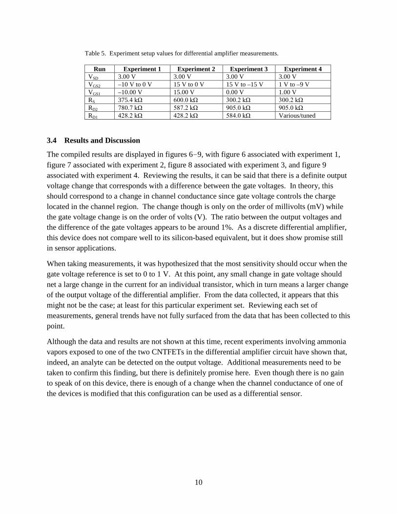
Table 1. Process flow description for the fabrication of a CNTFET. .............................................3 Table 2. Experiment setup values for the two primary measurements taken for CNTFETs. .........4 Table 3. Experiment setup values for additional measurements taken for CNTFETs. ...................5 Table 4. Measurement overview for CNTFETs on two samples and five structures/cells. ............6 Table 5. Experiment setup values for differential amplifier measurements. ................................10

1
1. Introduction and Background
Since their discovery, carbon nanotubes (CNTs) have been extensively studied for their great potential in a variety of applications. Sensors, interconnects, and specialty circuits are all key areas of interest for CNT-based devices. Several desirable properties that CNTs possess include a high thermal conductivity, high electrical mobility, high electrical current capacity, high tensile strength, small size, compatibility with current semiconductor fabrication processes, and ability to be functionalized.
The CNT-based field effect transistor (CNTFET) was demonstrated in 1998, and has opened the door to many avenues of research. Based on the semiconducting, single-walled carbon nanotube (SWNT), CNTFETs display similar behavior to their silicon (Si) metal-oxide-semiconductor FET (MOSFET) equivalents. An oxide film is placed in between a conductive gate and the SWNTs, which act as the channel of the transistor. Conductive metal contacts on either end of the SWNTs act as the source and drain. A bottom-gate transistor design is typically used, allowing for the SWNT channel to be exposed. This is convenient for sensor applications since the exposed CNT-based channel can be used to detect a variety of analytes via functionalization of the CNTs.
CNT-based sensors take advantage of the chemisorption of compounds onto its surface. The compounds that can be chemisorbed onto the CNT are determined by the functionalization of the CNT. In the case of a CNTFET with an exposed channel, the chemisorption of a particular compound changes the channel conductance of the CNTFET, and thus changes the source-drain current flowing through the device. The mechanism that causes the channel conductance change is still not yet confirmed, but there are a few dominant theories, including the adsorption of the compound affecting the dielectric constant of the CNTs and the charge transfer from the adsorbed compound causing a change in electrical conduction.
The motivation behind this research is to show proof-of-concept circuits for a CNT-based sensor that can eventually be integrated into a portable system carried by a U.S. Soldier. The circuits would make use of p-channel, depletion-mode transistors built out of SWNTs with metal contacts. Such sensors could potentially be used for detecting chemical and biological agents in the field with a minimal physical and energy footprint, such as an integrated device woven into the uniform or part of an electronics package carried by the Soldier. Further, this research lays the groundwork and provides a building block for a variety of other CNT-based circuits for analog and radio frequency (RF) applications.

2
2. CNTFET Device Characterization
2.1 Introduction
An important first step in the research was to characterize the current CNTFET devices that the U.S. Army Research Laboratory (ARL) produced in-house. This was done to gain a better understanding of the electrical characteristics and behavior of the devices. It also helped to dictate how and what applications they could potentially be used in as well as guide fabrication process changes that could potentially improve electrical performance in future CNTFET devices.
2.2 Device Structure and Fabrication
The devices tested were back-gate, depletion-mode, p-channel FETs with undoped CNT channels and titanium (Ti)-gold (Au) source/drain metal contacts. The n++ doped substrate comprised the common gate, and a 500-nm-thick silicon oxide (SiO2) layer acted as the gate insulator. Initial CNTFET device samples tested were fabricated using typical semiconductor fabrication processes including chemical vapor deposition (CVD) to grow the CNTs, e-beam evaporation to lay down source and drain contacts, and photolithography for patterning channel regions and contact regions. A full process flow for the creation of the initial devices is presented in table 1.

3
Table 1. Process flow description for the fabrication of a CNTFET.
1 AMD cleaning of substrate The n++ Si substrate is cleaned using an acetone, isopropyl alcohol (IPA), and deionized (DI) water rinse.
2 Thermal oxidation A thin layer of thermal oxide is grown on the wafer to form the gate insulator layer.
3 Photoresist spin Photoresist is spun on the top layer of the wafer to protect the gate oxide from the next etch step.
4 Buffered oxide etch A buffered hydrofluoric (HF) acid solution is used to strip the oxide from the wafer everywhere but from the top, which is protected by the photoresist.
5 Photoresist removal An acetone soak is used to remove the photoresist. 6 Catalyst deposition After another cleaning step, iron or nickel catalyst particles are
deposited on the gate oxide surface by dipping the wafer into a suspended catalyst solution.
7 CVD CNT growth CNTs are grown on the wafer using a furnace flowed with carbon species (methane and ethylene) along with hydrogen gas.
8 Photolithography – metal contacts
Photoresist is spun on, patterned with ultraviolet (UV) light, and then developed on the wafer top to create contacts.
9 Metal deposition Ti-Au is deposited on top of the photoresist patterned contacts using e-beam evaporation for electrical pads.
10 Liftoff The wafer is submerged in a photoresist remover, such as MicroChem’s Remover PG, for a period of time where the photoresist is lifted off, removing unwanted metal with it and leaving only the contacts.
11 AID cleaning of devices A final acetone/IPA/DI water rinse is performed on the completed device, which now possesses the following stack (bottom-up): Si n++ substrate: bottom gate SiO2: gate insulator CNTs: channel material Ti-Au metal: source and drain contact pads
2.3 Experimental Setup and Procedure
Approximately 150 CNTFET devices on 2 samples (5 structures) were electrically characterized using a Keithley 4200 Semiconductor Characterization System and a Micromanipulator probe station with standard coaxial probes. Multiple experiments were run, but predominantly, the drain-source current (IDS) was reviewed against changing drain-source voltage (VDS) and gate voltage (VGS).
Two families of curves were produced for each CNTFET device measured. A drain-source current versus drain-source voltage was plotted with stepped gate voltage values, and a drain-source current versus gate voltage was plotted with stepped drain-source voltage values. These two sets of curves provided a good basis of information on the electrical properties of the CNTFET devices produced at ARL. Table 2 lists the setup values for the two main experiments performed. Figures 1 and 2 are typical plots of the families of curves that were collected for each of the CNTFETs measured.

4
Table 2. Experiment setup values for the two primary measurements taken for CNTFETs.
IDS-VDS Curve Sweeps with Stepped VGS IDS-VGS Curve Sweeps with Stepped VDS VDS Start Value: 0.0 V VGS Start Value: –30.0 V VDS Stop Value: –2.0 V (on drain) VGS Stop Value: 20.0 V VDS Step Value: 0.025 V VGS Step Value: 1.0 V VGS Starting Step: –15.0 V VDS Starting Step: 0.0 V VGS Ending Step: 15.0 V VDS Ending Step: –1.0 V (on drain) VGS Step Size: 5.0 V VDS Step Size: 0.25 V Hysteresis: Not measured Hysteresis: Not measured
Figure 1. Typical IDS-VDS family of curves for a measured CNTFET.
Figure 2. Typical IDS-VGS family of curves for a measured CNTFET.

5
Additional experiments were performed to determine a few additional properties of the CNTFETs. The high-field experiments mimicked the conditions of the IDS-VDS measurements, but with the distinction of sweeping a much larger VDS voltage range. Instead of sweeping from 0 to –2 V, the drain-source voltage was swept from 0 to –20 V, and in a few cases, up to –30 V. High field measurements were taken to determine the current capacity of the CNT channel, and to see if metallic CNTs could be burned off, leaving only the semiconducting CNTs.
Initial testing revealed that the CNTFETs were not fully saturating at VDS = –2V. Experiments were performed pushing the drain-source voltage sweeps past 25 V to determine when, if ever, the CNTFETs entered saturation. Experiments to determine the extent of electrical field hysteresis were performed as well. Information was gained about the “memory” of these CNTFETs. Table 3 lists the setup values of these two secondary experiments.
Table 3. Experiment setup values for additional measurements taken for CNTFETs.
High-Field/Saturation Experiments Hysteresis Experiments VDS Start Value: 0.0 V VGS Start Value: –30.0 V VDS Stop Value: –20.0 V (on drain) VGS Stop Value: 20.0 V VDS Step Value: 0.250 V VGS Step Value: 1.0 V VGS Starting Step: –15.0 V VDS Starting Step: 0.0 V VGS Ending Step: 15.0 V VDS Ending Step: –1.0 V (on drain) VGS Step Size: 5.0 V VDS Step Size: 0.5 V Hysteresis: Not measured Hysteresis: Return sweep (On)
2.4 Results and Discussion
From the vast amounts of data compiled, there are several trends that can be seen in the CNTFETs tested. Of the 151 devices tested, 90 of those CNTFETs exhibited some type of gate-controlled behavior (defined as a change in the drain-source current with a change in the applied gate voltage). This would indicate that there are typical yield issues associated with the current device fabrication process, and this can be associated to many different causes. Table 4 provides a measurement overview regarding the devices tested.

6
Table 4. Measurement overview for CNTFETs on two samples and five structures/cells.
Sample Section CNT063A Q2 CNT071C Q1 CNT071C Q2 CNT071C Q3 CNT071C Q4 Ids range (Vds = 2V, Vgs = –15V)
–11.7 nA to –47.6 µA
–114 nA to –20.0 µA
–4.90 nA to –54.4 µA
–10.7 µA to –77.0 µA
–370 nA to –32.7 µA
Igs range (Vgs =–15V) ON
–1.35 nA to –1.94 nA
–49.1 nA to –357 nA
–82.5 nA to –97.6 nA
–13.1 µA to –105 µA
–42.3 nA to –59.2 nA
Ids range (Vgs = 15V) OFF
–721 fA to 3.75 nA
36.3 nA to 45.3 nA
30.6 nA to 37.8 nA
1.60 µA to 20.8 µA
37.2 nA to 56.9 nA
Ids:Igs ratio range (Vgs = –15V)
0.92 to 8.96 1.07 to 24.1 0.84 to 436 1.03 to 2.10 0.99 to 815
No. of devices that saturate (Ids-Vds)
0 1 0 0 4
No. of devices w/ consistent Ids-Vgs
18 4 13 0 17
No. of devices that turn off fully
0 3 3 0 5
No. of devices with transistor-like behavior
19 14 25 0 32
No. of devices measured
19/24 18/48 36/48 32/48 43/48
With the exception of 2 out of 151 CNTFETs measured, no other device could reach saturation when the drain-source voltage (VDS) was swept from 0 to –2 V. It appears that the majority of the devices operate exclusively in a pre-saturation state between this applied VDS range. From additional high-field experiments, this appears to be true for many devices out to VDS = –10 V. The I-V characteristics appear to be very linear, and it can be said with much certainty that the majority of the devices fabricated in this manner resemble gate-controlled resistors. Drain-source current (IDS) is typically directly proportional to VDS. The output resistance (r0) is given by VDS/ IDS, which remains fairly constant in most of the CNTFET devices tested. The output resistance appears to change though with respect to the gate voltage, with an increase in gate voltage directly related to a decrease in output resistance. Figure 1 portrays this typical result.
It also seems that very few of the CNTFET devices fully turn off (i.e., IDS = 0 A) even when a strong positive bias is applied to the gate. Only 11 out of the 151 devices measured exhibited the ability to completely turn off, as portrayed in figures 2 and 3. This issue stems from the fact that both semiconducting and metallic CNTs are grown during the CVD growth process. The high-field experiments revealed a solution to this problem though. The metallic CNTs could be burned off when high enough current was pushed through tubes. A high positive bias was applied to the gate (VGS = 15 V) to keep the semiconducting CNTs from conducting and burning out as well. This resulted in a drop in current throughput for a given CNTFET, but it provided a means to fully close the CNTFET channel to current. Figures 3 and 4 display the results of using higher VDS fields to remove metallic CNTs from the CNTFET channel region.

7
Figure 3. IDS-VGS plots before metallic CNT removal.
Figure 4. IDS-VGS plots after metallic CNT removal.
High-field measurements were also taken to determine the robustness of the CNTFET channels. For the vast majority of the devices tested, the drain-source voltage could be pushed up to –20 V before the CNTs started to burn off due to the current. Saturation of the IDS-VDS plots was reviewed as well at higher fields to determine if more devices would saturate if pushed to a higher voltage. This appears not to be the case, though. For devices that appeared to be saturating or trending to saturate at VDS = –2 V, those devices all appeared to saturate at VDS = –20 V. For devices that did not show any evidence of saturating, pushing VDS out to –0 V did not net any additional devices that could reach saturation.

8
2.5 Future Improvements and Current Progress
From the results, the CNTFET devices that are currently produced typically have a fairly linear IDS-VDS response (devices do not saturate), the IDS current is typically in the tens of µA or less, and intrinsically do not “turn off” when a relatively large positive bias is applied to the gate. There are several steps that can be taken to potentially improve the electrical performance of the CNTFET device.
Thinning the gate oxide thickness would provide a boost in gate control of the current through the CNT channel by increasing the gate capacitance. Moving to an oxide with a higher dielectric constant would also accomplish this. Changing the metal contact stack to metals that have a better matched work-function and possess better bonding with the CNTs would help create a better CNT-metal interface, promoting more ohmic contacts. Increasing the number of CNTs in the channel would help increase current throughput of the transistor. This could be accomplished through the use of a patterned catalyst for CNT growth, or through the use of a substrate such as quartz that better facilitates the growth of CNTs.
Progress has already been made recently with the fabrication of devices with a palladium (Pd)-based metal contact, which provides a superior CNT-metal interface compared to the Ti-Au metal contact used on the previously measured devices. This change was done in the hopes that the reduced electronic barrier at the interface would help reduce unwanted, non-ideal effects. Preliminary results indicate that although yield is down due to adhesion issues, samples that did come out show a marked increase in the number of devices that could potentially saturate (IDS vs. VDS curves). Additional testing will be needed to confirm the results.
3. Differential Amplifier Circuit Characterization
3.1 Introduction
The differential amplifier is a base component in many types of active circuits and it is the foundation for the majority of operational amplifier designs. Differential amplifiers are also used extensively in sensor applications due to their ability to help amplify small signals and increase the signal-to-noise ratio. It is for these reasons that this research is investigating the construction of CNTFET-based differential amplifier circuits. It seems to be a natural step to go from measuring and characterizing individual CNTFET devices to constructing and characterizing fundamental circuits, and reviewing their potential in a variety of applications.

9
3.2 Circuit Configuration
A simple long-tail differential amplifier using two electrically matched CNTFETs and three potentiometers was set up for the initial testing. The long-tail design was chosen for its simplicity to get initial results, while limiting any complications that might arise from the use of a current mirror or other, more complex current source circuit. A schematic of the circuit used is shown in figure 5.
Figure 5. Schematic of the long-tail differential amplifier used for initial testing.
3.3 Experimental Setup and Procedure
The circuit was set up as pictured in figure 5 with power supplies attached to VS, VGS1, and VGS. Voltmeters were hooked up to each of the power supplies to monitor the voltages. A fourth voltmeter was hooked up between the VOUT terminals to measure the output voltage. The resistors were tuned so that when VGS1 = VGS2, the output voltage (VOUT) read 0.0 V.
For the first measurements, VS and VGS1 were held constant while VGS2 was changed to simulate the analyte. Changing VGS2 changed the channel conductance, which is what the presence of an analyte would do. Multiple experiments were performed with VGS1 set to different bias values. Depending on the reference point (set by VGS1), the difference between VGS1 and VGS2 would cause varying output voltage responses.
Four initial sets of measurements were performed on the differential amplifier circuit. In all four cases, the source-drain voltage supplied (VS) was kept the same at 3 V. The gate reference voltage (VGS1) was changed for each of the four cases while VGS2 was swept. The resistance values were adjusted for each circuit to tune VOUT to 0 V when VGS1 = VGS2. A table with the values for each of the four sets of measurements is shown in table 5.
+ -
+ -
VGS2
RD
RD
CNTFET
CNTFET GG GG
DD DD
SS SS
VOUT
R
VS
VGS1
10
Table 5. Experiment setup values for differential amplifier measurements.
Run Experiment 1 Experiment 2 Experiment 3 Experiment 4 VSD 3.00 V 3.00 V 3.00 V 3.00 V VGS2 –10 V to 0 V 15 V to 0 V 15 V to –15 V 1 V to –9 V VGS1 –10.00 V 15.00 V 0.00 V 1.00 V RS 375.4 kΩ 600.0 kΩ 300.2 kΩ 300.2 kΩ RD2 780.7 kΩ 587.2 kΩ 905.0 kΩ 905.0 kΩ RD1 428.2 kΩ 428.2 kΩ 584.0 kΩ Various/tuned
3.4 Results and Discussion
The compiled results are displayed in figures 6–9, with figure 6 associated with experiment 1, figure 7 associated with experiment 2, figure 8 associated with experiment 3, and figure 9 associated with experiment 4. Reviewing the results, it can be said that there is a definite output voltage change that corresponds with a difference between the gate voltages. In theory, this should correspond to a change in channel conductance since gate voltage controls the charge located in the channel region. The change though is only on the order of millivolts (mV) while the gate voltage change is on the order of volts (V). The ratio between the output voltages and the difference of the gate voltages appears to be around 1%. As a discrete differential amplifier, this device does not compare well to its silicon-based equivalent, but it does show promise still in sensor applications.
When taking measurements, it was hypothesized that the most sensitivity should occur when the gate voltage reference is set to 0 to 1 V. At this point, any small change in gate voltage should net a large change in the current for an individual transistor, which in turn means a larger change of the output voltage of the differential amplifier. From the data collected, it appears that this might not be the case; at least for this particular experiment set. Reviewing each set of measurements, general trends have not fully surfaced from the data that has been collected to this point.
Although the data and results are not shown at this time, recent experiments involving ammonia vapors exposed to one of the two CNTFETs in the differential amplifier circuit have shown that, indeed, an analyte can be detected on the output voltage. Additional measurements need to be taken to confirm this finding, but there is definitely promise here. Even though there is no gain to speak of on this device, there is enough of a change when the channel conductance of one of the devices is modified that this configuration can be used as a differential sensor.

11
Differential Amplifier Performance
-0.12
-0.1
-0.08
-0.06
-0.04
-0.02
0
0.02
-12 -10 -8 -6 -4 -2 0
Vgs Difference (Vgs2-Vgs1) [V]
V_ou
t [V]
High End VoutLow End Vout
Figure 6. Experiment 1 results—plots the output voltage range to the difference between the gate voltages. VGS2 = –10 to 0 V with VGS1 held at –10 V.
Differential Amplifier Performance
0
0.02
0.04
0.06
0.08
0.1
0.12
0 2 4 6 8 10 12 14 16
Vgs Difference (Vgs2-Vgs1) [V]
V_ou
t [V]
High End VoutLow End Vout
Figure 7. Experiment 2 results—plots the output voltage range to the difference between the gate voltages. VGS2 = 15 to 0 V with VGS1 held at 15 V.

12
Output Voltage of CNT Differential Amplifier
-20
-10
0
10
20
30
40
50
60
70
80
-30.00 -25.00 -20.00 -15.00 -10.00 -5.00 0.00
Difference between Vgs2 and Vgs1 (V)
Out
put V
olta
ge (m
V)
High End of Range Low End of Range Figure 8. Experiment 3 results—plots the output voltage range to the difference between the gate voltages.
VGS2 = –15 to 15 V with VGS1 held at –15 V.
Differential Amplifier Sensitivity
-20.0E-3
-10.0E-3
000.0E+0
10.0E-3
20.0E-3
30.0E-3
40.0E-3
50.0E-3
60.0E-3
-10.0E+0 -9.0E+0 -8.0E+0 -7.0E+0 -6.0E+0 -5.0E+0 -4.0E+0 -3.0E+0 -2.0E+0 -1.0E+0 000.0E+0
Gate Voltage Difference (V)
Out
put V
olta
ge (V
)
Minimum Average Maximum
Figure 9. Experiment 4 results—plots the output voltage range to the difference between the gate voltages. VGS2 = 1 V to –9 V with VGS1 held at 1 V.

13
4. Conclusions
Measurements from 151 devices helped provide a good picture of the electrical characteristics for the CNTFETs that were produced thus far, and have provided valuable information for determining improvements that can be made to the device fabrication process. The majority of the CNTFETs currently fabricated typically behave like gate-controlled resistors, with drain-source current leakage occurring most likely due to the presence of metallic carbon nanotubes. Improvements to the fabrication process will be made in hopes of improving the performance of the CNTFETs, and pushing the electrical characteristics closer to that of a silicon-based MOSFET.
Initial differential amplifier measurements were made with a simplistic long-tail design. The initial experiments indicate that a change in the channel conductance is reflected in a change in the output voltage, but this change is not amplified as it typically is for silicon-based differential amplifier circuits. For every 1 V difference between the two gates, the output voltage changes on the order of millivolts. Substantially more data will need to be collected and additional experiments will need to be performed to get a better picture of CNTFET-based differential amplifier circuits.
5. Next Steps
The foundation of the differential amplifier circuit is the CNTFETs that are used. Improvements to the CNTFET device and additional characterization of these devices will be a priority. Some changes that will be made in the next devices to be fabricated include changing the contact metal from gold to palladium, which should improve the ohmic nature of the contacts. The gate oxide will also be thinned, which should help with gate control. Gate insulators with a higher dielectric constant such as titanium oxide or aluminum oxide will be integrated into future devices for the better gate control. Increasing the density of the semiconducting carbon nanotubes between the source and the drain (channel region) could be done to improve channel conductivity and current capacity. All of these proposed changes to the current process could potentially increase the performance of the current CNTFETs used.
Additional measurements on the differential amplifier circuit also need to be taken. More data should be collected using a more diverse set of gate voltage references. Gas sensing data using an actual analyte is currently being collected with more being taken to get an idea of how an analyte could potentially affect electrical performance. Also, alternative circuit designs for the differential amplifier should be taken into consideration. Using a current mirror or a different

14
constant current source circuit instead of a long-tail resistor could help improve the performance of the differential amplifier. Much of the initial data collected shows the potential of this circuit for sensor applications, but there is much more that can be done to improve our understanding of these CNTFET devices and their associated circuits.

15
List of Symbols, Abbreviations, and Acronyms
ARL U.S. Army Research Laboratory
Au gold
CNTFET CNT-based field effect transistor
CNTs carbon nanotubes
CVD chemical vapor deposition
DI deionized
FET field effect transistor
HF hydrofluoric
IPA isopropyl alcohol
MOSFET metal-oxide-semiconductor FET
Pd palladium
RF radio frequency
Si silicon
SiO2 silicon oxide
SWNT single-walled carbon nanotube
Ti titanium
UV ultraviolet

16
No. of Copies Organization 1 ADMNSTR ELECT DEFNS TECHL INFO CTR ATTN DTIC OCP 8725 JOHN J KINGMAN RD STE 0944 FT BELVOIR VA 22060-6218 1 CD OFC OF THE SECY OF DEFNS ATTN ODDRE (R&AT) THE PENTAGON WASHINGTON DC 20301-3080 1 US ARMY RSRCH DEV AND ENGRG CMND
ARMAMENT RSRCH DEV AND ENGRG CTR ARMAMENT ENGRG AND TECHNLGY CTR
ATTN AMSRD AAR AEF T J MATTS BLDG 305 ABERDEEN PROVING GROUND MD 21005-5001 1 PM TIMS, PROFILER (MMS-P) AN/TMQ-52 ATTN B GRIFFIES BUILDING 563 FT MONMOUTH NJ 07703 1 US ARMY INFO SYS ENGRG CMND ATTN AMSEL IE TD A RIVERA FT HUACHUCA AZ 85613-5300 1 COMMANDER US ARMY RDECOM ATTN AMSRD AMR W C MCCORKLE 5400 FOWLER RD REDSTONE ARSENAL AL 35898-5000
No. of Copies Organization 1 US GOVERNMENT PRINT OFF DEPOSITORY RECEIVING SECTION ATTN MAIL STOP IDAD J TATE PITOL ST NW WASHINGTON DC 20402 1 OREGON STATE UNIV SCHOL OF ELECT ENGRG AND COMPUTER SCI ATTN M. CHIN 1148 KELLEY ENGINEERING CENTER CORVALLIS OR 97331-4501 1 US ARMY RSRCH LAB ATTN RDRL CIM G T LANDFRIED BLDG 4600 ABERDEEN PROVING GROUND MD 21005-5066 15 US ARMY RSRCH LAB ATTN IMNE ALC HRR MAIL & RECORDS MGMT ATTN RDRL CIM L TECHL LIB ATTN RDRL CIM P TECHL PUB ATTN RDRL SE J PELLEGRINO ATTN RDRL SER E P AMIRTHARAJ ATTN RDRL SER E R DEL ROSARIO ATTN RDRL SER L B NICHOLS ATTN RDRL SER L B PIEKARSKI ATTN RDRL SER L C ANTON ATTN RDRL SER L M DUBEY ATTN RDRL SER L M ERVIN ATTN RDRL SER L S KILPATRICK ATTN RDRL SER M E ADLER ATTN RDRL SER U K KAPPRA ATTN RDRL SES E T KIPP ADELPHI MD 20783-1197 TOTAL: 24 (22 HCS, 1 CD, 1 ELECT)