Embed Size (px)
Citation preview

Diamonds at CHESS and BNL
report from meeting with BNL Instrumentation group working to produce thin diamond monocrystals for use as a fast electron multiplier
Richard Jones, University of Connecticutfor the
GlueX Photon Beam working group
GlueX collaboration meeting, Newport News, Jan. 29-31, 2009

GlueX collaboration meeting, Newport News, Jan. 29-31, 2009 2
Updates
report from meeting at BNL new sources for diamonds plans for CHESS run this Spring

GlueX collaboration meeting, Newport News, Jan. 29-31, 2009 3
Report from meeting at BNL Jan. 14, 2009: E. Aschenaur, J. Stewart, R. Jones met at
BNL with T. Rao, J. SmedleyJ. Smedley,, and others.
T. Rao group: diamond R&D for instrumentation diamond detectordiamond detector – rad-hard replacement for silicon detectors diamond multiplierdiamond multiplier – fast current amplifier for ERL source
Special requirements for diamond electronics: diamond is a large-gap semiconductordiamond is a large-gap semiconductor major problem – carriers get trapped in localized states in the gapmajor problem – carriers get trapped in localized states in the gap large gap – trapping lifetimes very long at room temperaturelarge gap – trapping lifetimes very long at room temperature requires extremely low impurity concentrations – requires extremely low impurity concentrations – type IIItype III also requires very low defect density –also requires very low defect density – large monocrystalslarge monocrystals multiplier application requires fast responsemultiplier application requires fast response – thin samples – thin samples

GlueX collaboration meeting, Newport News, Jan. 29-31, 2009 4
How the multiplier works
z
E
Vbias
incidentelectron
valence band
conduction band
0

GlueX collaboration meeting, Newport News, Jan. 29-31, 2009 5
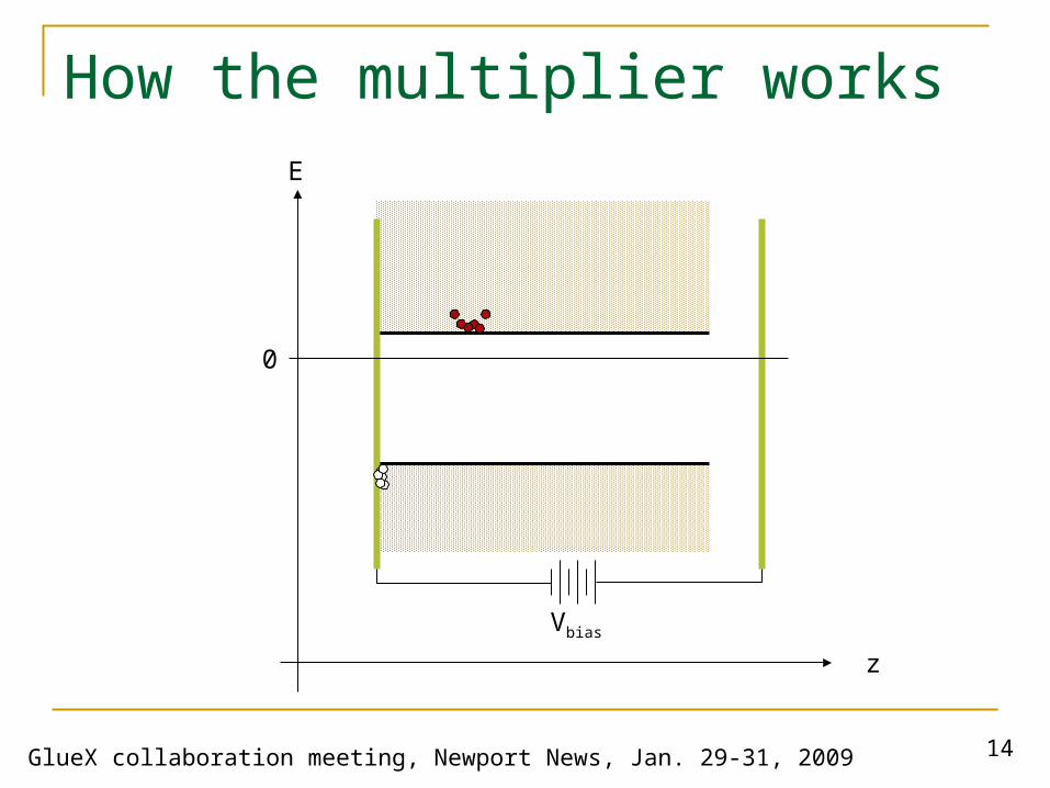
How the multiplier works
z
E
Vbias
incidentelectron
0
holes
electrons

GlueX collaboration meeting, Newport News, Jan. 29-31, 2009 6
How the multiplier works
z
E
Vbias
0

GlueX collaboration meeting, Newport News, Jan. 29-31, 2009 7
How the multiplier works
z
E
Vbias
0

GlueX collaboration meeting, Newport News, Jan. 29-31, 2009 8
How the multiplier works
z
E
Vbias
0

GlueX collaboration meeting, Newport News, Jan. 29-31, 2009 9
How the multiplier works
z
E
Vbias
0

GlueX collaboration meeting, Newport News, Jan. 29-31, 2009 10
How the multiplier works
z
E
Vbias
0

GlueX collaboration meeting, Newport News, Jan. 29-31, 2009 11
How the multiplier works
z
E
Vbias
0

GlueX collaboration meeting, Newport News, Jan. 29-31, 2009 12
How the multiplier works
z
E
Vbias
0

GlueX collaboration meeting, Newport News, Jan. 29-31, 2009 13
How the multiplier works
z
E
Vbias
0
GlueX collaboration meeting, Newport News, Jan. 29-31, 2009 14
How the multiplier works
z
E
Vbias
0

GlueX collaboration meeting, Newport News, Jan. 29-31, 2009 15
How the multiplier works
z
E
Vbias
0
GlueX collaboration meeting, Newport News, Jan. 29-31, 2009 16
How the multiplier works
z
E
Vbias
0

GlueX collaboration meeting, Newport News, Jan. 29-31, 2009 17
How the multiplier works
z
E
Vbias
0

GlueX collaboration meeting, Newport News, Jan. 29-31, 2009 18
How the multiplier works
z
E
Vbias
0

GlueX collaboration meeting, Newport News, Jan. 29-31, 2009 19
How the multiplier works
z
E
Vbias
0

GlueX collaboration meeting, Newport News, Jan. 29-31, 2009 20
How the multiplier works
z
E
Vbias
0

GlueX collaboration meeting, Newport News, Jan. 29-31, 2009 21
How the multiplier works
z
E
Vbias
0

GlueX collaboration meeting, Newport News, Jan. 29-31, 2009 22
How the multiplier works
z
E
Vbias
0

GlueX collaboration meeting, Newport News, Jan. 29-31, 2009 23
How the multiplier works
z
E
Vbias
0

GlueX collaboration meeting, Newport News, Jan. 29-31, 2009 24
How the multiplier works
z
E
Vbias
0

GlueX collaboration meeting, Newport News, Jan. 29-31, 2009 25
How the multiplier works
z
E
Vbias
0

GlueX collaboration meeting, Newport News, Jan. 29-31, 2009 26
How the multiplier works
z
E
Vbias
0

GlueX collaboration meeting, Newport News, Jan. 29-31, 2009 27
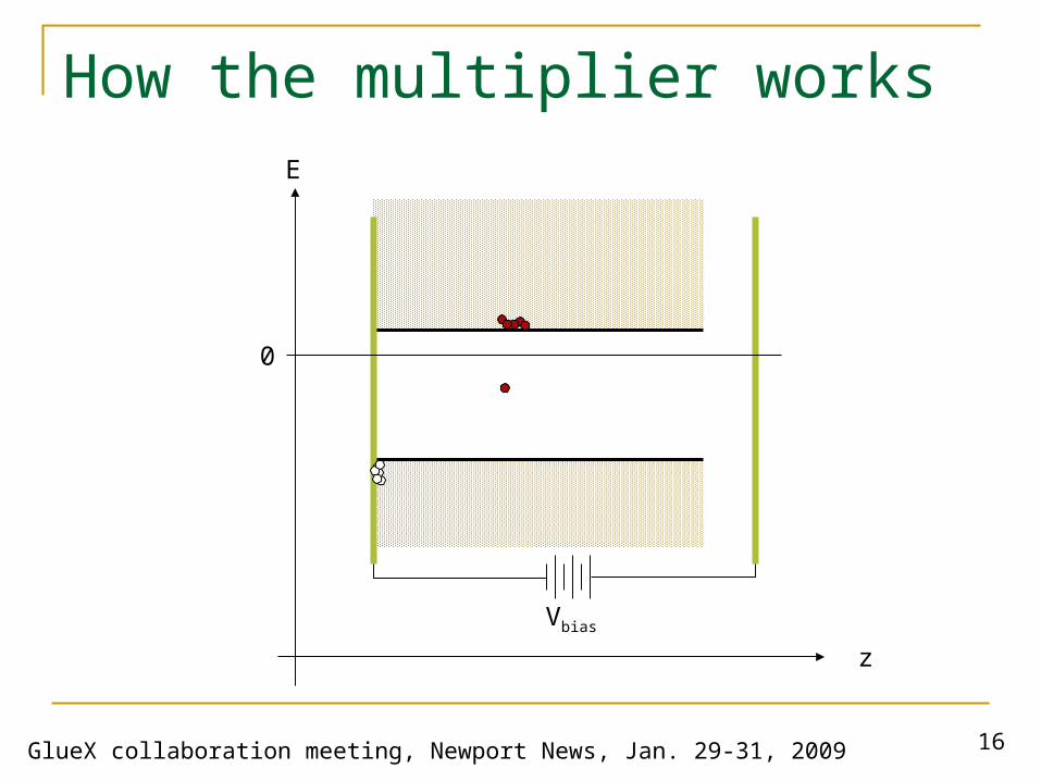
How the multiplier works
z
E
Vbias
0 free e- energyfor same k
traps
pulse broadenedby diffusion

GlueX collaboration meeting, Newport News, Jan. 29-31, 2009 28
Diamond multiplier requirements ERL source amplifier: pulse length ~few ps Preserve short pulses: < 30 microns thickness R&D goal for multiplier: 20-30 microns20-30 microns
Trapping a problem at high currents Requires very low impurity concentrations (ppb) Requires very perfect monocrystals – low defect density Only CVD monocrystals meet this requirement
CVD diamonds with ppb nitrogen now available from CVD diamonds with ppb nitrogen now available from Element Six, Sumitomo Electric, Apollo – Element Six, Sumitomo Electric, Apollo – type IIItype III

GlueX collaboration meeting, Newport News, Jan. 29-31, 2009 29
Diamond Thinning Lab @ BNL Review: known ways to mill diamond
1. lapping Known to work, used to mill diamonds for Hall B Often destroys the sample, low yield Y high cost
2. reactive ion etching
3. focused ion beam milling
4. electron cyclotron resonance etching
5. inductively coupled plasma etching
6.6. laser ablationlaser ablation
“they are generally slow and prohibitive processes if significant thickness reduction or large aspect ratio structures are required.” J. Smedley et.al., preprint
under active development by BNL groupunder active development by BNL group

GlueX collaboration meeting, Newport News, Jan. 29-31, 2009 30
Diamond Thinning Lab @ BNL Laser ablation: small-scale equivalent of dynamite
1x1 mm2 square region of CVD diamond scanned with 50 micron pitch, 266 nm light (4’th harmonic NdYAG), 30 ps pulses, focal spot size 27 microns rms, varying energy per pulse.

GlueX collaboration meeting, Newport News, Jan. 29-31, 2009 31
Diamond Thinning Lab @ BNL
Groove pattern left by ablation withsweeps separated by 50 microns
Opticalmicroscopeimages
SEM imageof surface
before ozone cleaning
after ozone cleaning
note: internaldamage atgrain boundariesof polycrystal

GlueX collaboration meeting, Newport News, Jan. 29-31, 2009 32
Diamond Thinning Lab @ BNLSame, but with 5 micron pitch between scans
optical microscope image(before cleaning)
atomic force microscope surface profiles
dark regions are damagezones at polycrystal boundaries,gray bands are amorphous carbon surface layer ~60 nm thick

GlueX collaboration meeting, Newport News, Jan. 29-31, 2009 33
Diamond Thinning Lab @ BNL
Same as before, but using laser with 20 ns pulses
Several variations were tried, results were not as good
Using 532 nmlaser light, instead of 266 nm
GlueX collaboration meeting, Newport News, Jan. 29-31, 2009 34
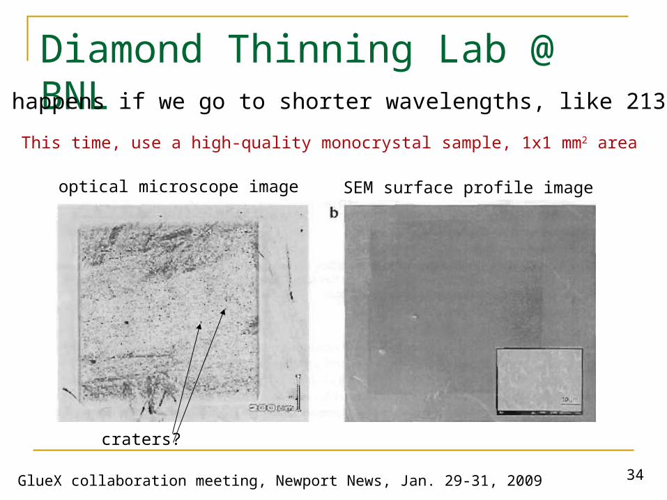
Diamond Thinning Lab @ BNLWhat happens if we go to shorter wavelengths, like 213 nm?
optical microscope image SEM surface profile image
This time, use a high-quality monocrystal sample, 1x1 mm2 area
craters?

GlueX collaboration meeting, Newport News, Jan. 29-31, 2009 35
Diamond Thinning Lab @ BNL
Normal surfaceroughness is p-p~ 0.1 microns
Craters are deeper, up to ~0.5 microns
Ablation depth1.5 microns(not a limit)
Edge slope: 10:1

GlueX collaboration meeting, Newport News, Jan. 29-31, 2009 36
Diamond Thinning Lab @ BNL Next steps being pursued at BNL
Conduct tests with new Excimer (193 nm) laser. Try reactive ion etching post-processing step to
smooth out remaining surface roughness. Improved electrode deposition tests. Correlate electron transfer with defect densities
in the crystal
Ablate a region of a diamond down to 20 microns.
and eventually …
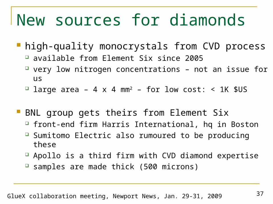
GlueX collaboration meeting, Newport News, Jan. 29-31, 2009 37
New sources for diamonds high-quality monocrystals from CVD process
available from Element Six since 2005 very low nitrogen concentrations – not an issue for us large area – 4 x 4 mm2 – for low cost: < 1K $US
BNL group gets theirs from Element Six front-end firm Harris International, hq in Boston Sumitomo Electric also rumoured to be producing these Apollo is a third firm with CVD diamond expertise samples are made thick (500 microns)

GlueX collaboration meeting, Newport News, Jan. 29-31, 2009 38
Plans for 2009 run at CHESS planned for April
BNL group agrees to loan us a type III CVD sample from their inventory to run whole-crystal rocking curve.
Hall B has a diamond for which the full radiation exposure map is available – in principle. We plan to map this diamond along both (2,2,0) axes.
collaboration with BNL on thinning potential for real cost savings! we need our own diamond inventory for studies have contact with Harris International, meeting planned once diamonds are in-hand, will pursue arrangements with the
BNL group to use their thinning facilites – ca. Fall 2009 manpower needed – UConn seeking funding for a postdoc