Embed Size (px)
Citation preview

This is an electronic reprint of the original article.This reprint may differ from the original in pagination and typographic detail.
Powered by TCPDF (www.tcpdf.org)
This material is protected by copyright and other intellectual property rights, and duplication or sale of all or part of any of the repository collections is not permitted, except that material may be duplicated by you for your research use or educational purposes in electronic or print form. You must obtain permission for any other use. Electronic or print copies may not be offered, whether for sale or otherwise to anyone who is not an authorised user.
Di Marco, A.; Maisi, Ville; Hekking, F.W.J.; Pekola, J.P.
Effect of photon-assisted Andreev reflection in the accuracy of a SINIS turnstile
Published in:PHYSICAL REVIEW B
DOI:10.1103/PhysRevB.92.094514
Published: 28/09/2015
Document VersionPublisher's PDF, also known as Version of record
Please cite the original version:Di Marco, A., Maisi, V., Hekking, F. W. J., & Pekola, J. (2015). Effect of photon-assisted Andreev reflection in theaccuracy of a SINIS turnstile. PHYSICAL REVIEW B, 92(9), 1-12. [094514]. DOI: 10.1103/PhysRevB.92.094514

PHYSICAL REVIEW B 92, 094514 (2015)
Effect of photon-assisted Andreev reflection in the accuracy of a SINIS turnstile
A. Di Marco,1,* V. F. Maisi,2,3,† F. W. J. Hekking,1 and J. P. Pekola3
1LPMMC-CNRS, Universite Grenoble-Alpes, 25 Avenue des Martyrs BP 166, F-38042 Grenoble Cedex, France2Centre for Metrology and Accreditation (MIKES), P.O. Box 9, FI-02151 Espoo, Finland
3Low Temperature Laboratory, Aalto University, P.O. Box 13500, FI-00076 Aalto, Finland(Received 15 July 2015; published 28 September 2015)
We consider a hybrid single-electron transistor constituted by a gate-controlled normal-metal island (N)connected to two voltage-biased superconducting leads (S) by means of two tunnel junctions (SINIS), operatedas a turnstile. We show that the exchange of photons between this system and the high-temperature electromagneticenvironment where it is embedded enhances Andreev reflection, thereby limiting the single-electron tunnelingaccuracy.
DOI: 10.1103/PhysRevB.92.094514 PACS number(s): 73.23.Hk, 74.78.Na, 85.25.−j, 74.55.+v
I. INTRODUCTION
The experimental realization of a quantum electric currentstandard is one of the scientific and technological challengesof the present time. This is a key goal in metrology becauseit would lead to a modern definition of ampere as well as tothe most accurate comparison of the fundamental constantsRK = h/e2 and KJ = 2e/h [1]. Among the devices proposedup to now [2–7], the hybrid SINIS single-electron transistor(SET) depicted in Fig. 1 is one of the most interestingcandidates [8]. Such a device is formed of a normal-metal(N) island joined to two superconducting (S) electrodes viatwo tunnel junctions with capacitances CS for the source(S) and CD for the drain (D). The entire structure is biasedwith a constant voltage VD − VS = V . The amount of electriccharge localized on the island is controlled using a gatepotential Vg(t), capacitively coupled to N by means of agate with capacitance Cg . Typically, the charging energy ofthe island EC = e2/2C� , with C� = CS + CD + Cg , governsthe tunneling processes in the SET, i.e., the system works inthe Coulomb blockade regime. Additional energy filtering isprovided by the two outer superconductors which protect thedevice against unwanted tunneling events. In this context, ifsingle-electron tunneling is the dominant process, a periodicVg(t) signal with frequency f generates an electric current I
through the SET which is equal to ef . In other words, theSET is a frequency-to-current converter. However, high-ordertunneling events occur in addition to the single-particle ones.They limit the conversion accuracy of this electronic turnstile,thereby acting as error sources. The main contribution tothe total error is usually provided by elastic and inelasticcotunneling [9,10] as well as Andreev reflection and Cooper-pair cotunneling [11,12]. From a theoretical point of view, ithas been shown that all these processes can be eliminatedefficiently, thereby reaching the metrological requirements[11]. Nevertheless, in real experiments the achievement of theaccuracy needed for the completion of the so-called quantum
*Present address: Department of Nanotechnology and Nanoscience(MC2), Chalmers University of Technology, SE-41298 Goteborg,Sweden.
†Present address: Solid State Physics Laboratory, ETH Zurich, CH-8093 Zurich, Switzerland.
SS N
VD =V/2Vg
Cg
CS CDsource island drain
VS = −V/2
FIG. 1. Hybrid SINIS single-electron transistor (SET). The blackparts stand for the insulating barriers of the tunnel junctions.
metrological triangle remains a difficult task. In particular, anoise-induced residual Andreev tunneling current affects theI -V characteristic of the SET turnstile, although the increase ofthe charging energy EC , with respect to the gap parameter � ofthe superconductors, leads to a decrease of Andreev reflectionprobability [12]. Such a two-electron current may be due to theeffect of the high-temperature electromagnetic environmentthe SINIS device is coupled with. The energy provided bysuch an external thermal bath to the SET via the exchangeof photons can promote tunneling of particles through thesingle junction [13–15]. In this paper, we show that, indeed,the environment-assisted Andreev reflection limits the turnstileaccuracy, unless it is properly taken care of.
II. ELECTRONIC TRANSPORT IN A SINIS TURNSTILE
In the Coulomb blockade regime, the electronic transportin the SINIS device of Fig. 1 is determined by the chargingenergy EC . For a symmetric device, CS = CD = C, assumingthat initially the excess electric charge localized on the islandis −ne, with n an integer, the energy cost to add (+N , in)or remove (−N , out) N extra electrons to or from the centralnormal-metal electrode is given by
Ein/outD (n,N ) ≡ ED
island(n ± N ) − EDisland(n)
= ECN2 ± 12eV N ± 2EC(n − ng)N, (1)
if the tunneling process occurs through the drain (D), and
Ein/outS (n,N ) ≡ ES
island(n ± N ) − ESisland(n)
= ECN2 ∓ 12eV N ± 2EC(n − ng)N, (2)
1098-0121/2015/92(9)/094514(12) 094514-1 ©2015 American Physical Society

DI MARCO, MAISI, HEKKING, AND PEKOLA PHYSICAL REVIEW B 92, 094514 (2015)
(a) (b) (c)
FIG. 2. (Color online) Close view of the overlapping region between the Coulomb diamonds for n = 0 and n = 1 obtained using(a) EC/� = 1, (b) EC/� = 0.6, and (c) EC/� = 2. Also shown are the single- (dashed blue lines) and two-particle (dashed red lines)thresholds and the optimal loop (solid black lines) at eV � � from ng = ng,1 to ng = ng,2.
when the insulating barrier of the source (S) is overcome.In Eqs. (1) and (2), the total energy of the island Ei
island(n ±N ), with i = S,D, is the difference between the electrostaticenergy due to the Coulomb interactions involving also theinduced charge, and the work done by all the voltage sources toincrease or decrease n with the tunneling of N particles throughone of the insulating layers; ng = CgVg/e is the gate-inducedcharge [16,17].
A. Single-electron tunneling
Due to the energy gap in the BCS density of states of asuperconductor, single-electron tunneling events (N = 1) areenergetically allowed above the gap, i.e., when the changesin energy Eqs. (1) and (2) are smaller than −�. On thecontrary, above −� the excess charge −ne of the islandremains fixed to its initial value. Per each n, the thresholdconditions E
in/outD (n,1) = −� and E
in/outS (n,1) = −� give rise
to four crossing lines in the plot of the total bias voltage V as afunction of the gate-induced charge ng . The four intersectionpoints between these lines are the edges of the so-calledCoulomb diamond, which is a stability region for the system.This means that no single-electron tunneling process can occurfor the values of V and ng within its area. Unlike the case of afully normal SET, NININ, the Coulomb diamonds for a SINISdevice corresponding to different n overlap. Specifically, whenEC ∼ �, the stability region for a given n shares two distinctportions of the V vs ng plane with the n + 1 and n − 1diamonds, i.e., in each overlapping area at most two differentvalues of n are stable. This feature is at the basis of thegeneration of a controlled and synchronized single-electroncurrent through the hybrid single-island structure of Fig. 1. Inthis regard, let us consider, for instance, the plot of Fig. 2(a)where a close view of the Coulomb diamonds corresponding ton = 0 and n = 1 and their shared part are shown. In principle,to have a cycle corresponding to a single-particle transfer fromthe source to the drain, ng has to move along a closed path inthe V vs ng plane which connects the diamonds where n = 0and n = 1 are stable. Owing to the presence of the overlappingregion, this kind of connection can be realized by avoiding thepart of the plane where both n = 0 and n = 1 are unstable.As a result, each single-electron tunneling event to/from thecentral island can be controlled by means of the gate potentialVg . During each cycle of ng along the working loop, thebias voltage V is usually kept fixed close to �/e. For this
optimal value, the superconducting energy gap � guaranteesan efficient suppression of thermally activated tunneling eventsand quasiparticle excitations as well as elastic and inelasticcotunneling processes [8,11]. A typical loop used in realexperiments with these features is shown in Fig. 2(a). Startingfrom ng = ng,1, the number of excess electrons localized onthe island, whose initial value is n = 0, remains constant untilthe threshold Sin(0,1), defined by the equation Ein
S (0,1) = −�,is crossed. At that point one electron can enter in the centralelectrode via the source junction and n passes from 0 to 1. Onceng = ng,2 is reached, the closed path is covered backward. Theextra electron on the island can tunnel out through the drainonly after overcoming the threshold Dout(1,1), given by theequation Eout
D (1,1) = −�. When ng is again equal to ng,1, theisland is back in its initial state and a new cycle can start.Since per each cycle exactly one electron is transferred fromthe source to the drain, driving ng from ng,1 to ng,2 and backto ng,1 with a signal with frequency f allows one to generatethe single-electron current I = ef .
B. Andreev reflection and higher-order processes
In addition to single-electron tunneling events, the currentflowing through a SINIS transistor is, in general, also affectedby the Andreev reflection, i.e., the transfer of two electronsper unit of time inside or outside the island [18,19]. Thissecond-order tunneling process is insensitive to the energybarrier provided by the superconducting gap. This meansthat the rate of the transitions n → n ± 2 can be relevantalthough the device is working at the optimal bias, eV � �.As a result, the Coulomb diamonds for the Andreev reflectionevents are obtained just imposing that the energies Eqs. (1)and (2) for N = 2 are smaller than zero. However, as shown inFigs. 2(b) and 2(c), the energy �, together with the chargingenergy EC , plays an important role in the determination ofthe two-electron tunneling probability. If the ratio EC/� issmaller than 1, the Andreev diamonds are contained withinthe single-particle stability regions. In this case, we seefrom Fig. 2(b) that the optimal loop crosses the two-particlethreshold Sin(0,2), given by the equation Ein
S (0,2) = 0, beforethe single-electron line Sin(0,1), while going from ng,1 tong,2. When ng is decreased back to ng,1, the closed pathovercomes Dout(1,1) after Dout(1,2), the line correspondingto Eout
D (1,2) = 0. It follows that, in this regime, the controlof single-electron tunneling is compromised by the Andreev
094514-2
EFFECT OF PHOTON-ASSISTED ANDREEV REFLECTION . . . PHYSICAL REVIEW B 92, 094514 (2015)
transitions 0 → 2 and 1 → −1. On the other hand, whenEC/� > 1, the single-particle diamonds are smaller than theones for Andreev reflection. Now, the two-particle thresholdscan be avoided, as shown in Fig. 2(c), thereby suppressing theprobability to increase/decrease the charge of the island by twoelectrons per each tunneling event.
However, higher-order processes, such as the cotunnelingof one electron and one Cooper pair [11], can occur whileng covers the loop of Fig. 2(c). They can limit the single-electron transfer accuracy even if EC/� > 1. In particular,the more the system stays in the overlapping region wheremore than one charge state is stable, the bigger the effectof unwanted transitions would be. To decrease the influenceof the higher-order error events, the signal ng(t), which isusually used to go from ng,1 to ng,2 and back to ng,1, is asquare wave. This choice guarantees that the time spent inbetween ng,1 and ng,2 is minimized. On the other hand, theperiod τ = 1/f of ng(t) has to be long enough in order for thesingle-particle tunneling processes to take place. If the numbern changes by one electron with the rate �1e, then the tunnelingerror or probability that the charge of the island remains thesame is ε ∼ exp(−�1e/2f ). In particular, the requirementε � εmetr = 10−8 has to be satisfied for the definition of thequantum current standard. This means that �1e � 109 s−1
because the trade-off between the missed tunneling discussedabove and the leakage by Cooper-pair–electron cotunnelinglimits the maximum operation frequency to f ∼ 60 MHz toachieve the metrologically accurate current I = ef ∼ 10 pAfor a single SINIS turnstile [11,20,21].
III. ENVIRONMENT-ASSISTED ANDREEV REFLECTION
A. Effect of the electromagnetic environmenton the electronic transport
As discussed in the previous section, the tunneling pro-cesses involving more than one electron may be reduced bybiasing the SINIS turnstile at the optimal value eV � �,considering EC/� > 1 and using for ng(t) a square-wave-likesignal which oscillates with frequency f between the twoinduced-gate charges ng,1 and ng,2 of Fig. 2(c). Under theseconditions, one expects to measure the current I = ef with arelatively high accuracy. In principle, it should be possible evento go below the relative error εmetr required by the metrologicalapplications. However, in real experiments, the achievement ofthe accuracy needed for the definition of the quantum currentstandard still remains a difficult task.
The coupling of the hybrid turnstile with its surroundinghigh-temperature electromagnetic environment may be a detri-mental source of error [13]. Indeed, the absorption/emissionof energy from/to such a thermal bath allows the tunnelingof electrons, even when overcoming the insulating barrier isenergetically forbidden for a well isolated SET. Nevertheless,the environment-assisted tunneling of quasiparticles can beefficiently suppressed using, for instance, an on-chip capaci-tively coupled ground plane [13] and/or by means of a highlyresistive transmission line [14,22]. The main contributionto the leakage current observed in the I -V characteristicis typically due to the Andreev reflection. Although largecharging energies, EC > �, should reduce the probability for
RTRT
V2Vg
Z1 Z2Zg
Cg
source island drain
−V2
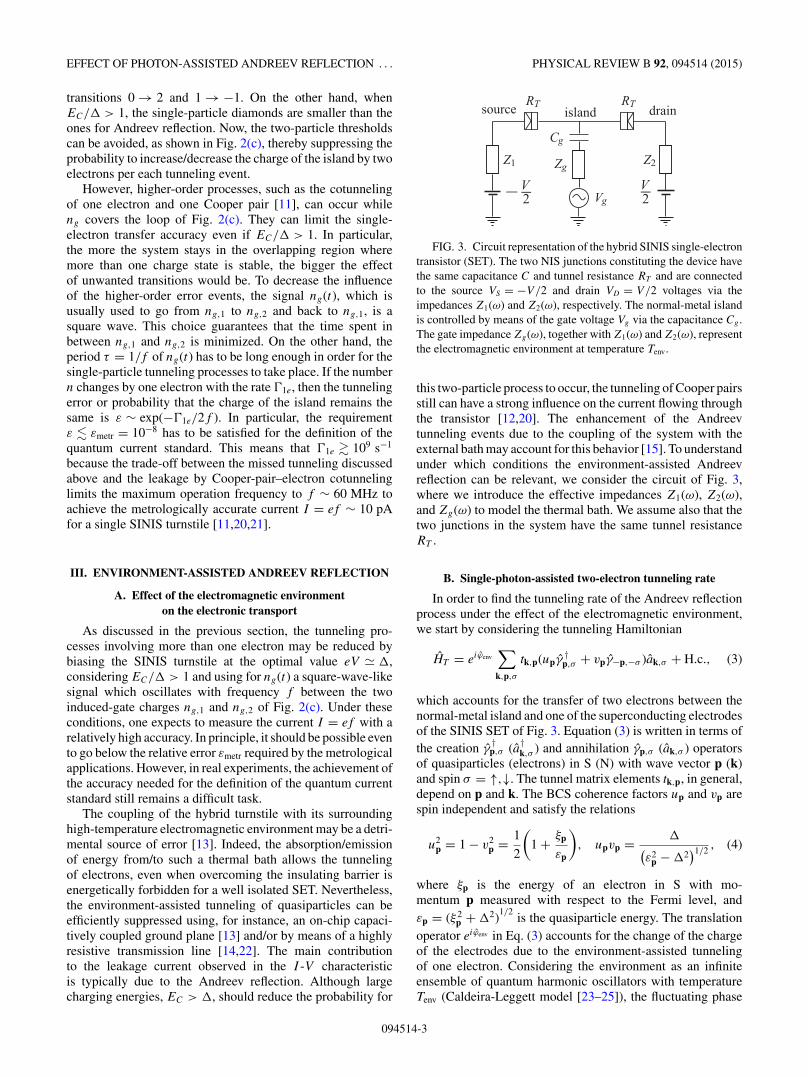
FIG. 3. Circuit representation of the hybrid SINIS single-electrontransistor (SET). The two NIS junctions constituting the device havethe same capacitance C and tunnel resistance RT and are connectedto the source VS = −V/2 and drain VD = V/2 voltages via theimpedances Z1(ω) and Z2(ω), respectively. The normal-metal islandis controlled by means of the gate voltage Vg via the capacitance Cg .The gate impedance Zg(ω), together with Z1(ω) and Z2(ω), representthe electromagnetic environment at temperature Tenv.
this two-particle process to occur, the tunneling of Cooper pairsstill can have a strong influence on the current flowing throughthe transistor [12,20]. The enhancement of the Andreevtunneling events due to the coupling of the system with theexternal bath may account for this behavior [15]. To understandunder which conditions the environment-assisted Andreevreflection can be relevant, we consider the circuit of Fig. 3,where we introduce the effective impedances Z1(ω), Z2(ω),and Zg(ω) to model the thermal bath. We assume also that thetwo junctions in the system have the same tunnel resistanceRT .
B. Single-photon-assisted two-electron tunneling rate
In order to find the tunneling rate of the Andreev reflectionprocess under the effect of the electromagnetic environment,we start by considering the tunneling Hamiltonian
HT = eiϕenv∑k,p,σ
tk,p(upγ†p,σ + vpγ−p,−σ )ak,σ + H.c., (3)
which accounts for the transfer of two electrons between thenormal-metal island and one of the superconducting electrodesof the SINIS SET of Fig. 3. Equation (3) is written in terms ofthe creation γ
†p,σ (a†
k,σ ) and annihilation γp,σ (ak,σ ) operatorsof quasiparticles (electrons) in S (N) with wave vector p (k)and spin σ = ↑,↓. The tunnel matrix elements tk,p, in general,depend on p and k. The BCS coherence factors up and vp arespin independent and satisfy the relations
u2p = 1 − v2
p = 1
2
(1 + ξp
εp
), upvp = �(
ε2p − �2
)1/2 , (4)
where ξp is the energy of an electron in S with mo-mentum p measured with respect to the Fermi level, andεp = (ξ 2
p + �2)1/2
is the quasiparticle energy. The translationoperator eiϕenv in Eq. (3) accounts for the change of the chargeof the electrodes due to the environment-assisted tunnelingof one electron. Considering the environment as an infiniteensemble of quantum harmonic oscillators with temperatureTenv (Caldeira-Leggett model [23–25]), the fluctuating phase
094514-3

DI MARCO, MAISI, HEKKING, AND PEKOLA PHYSICAL REVIEW B 92, 094514 (2015)
S
S
N
N
k1
k1
k2
k2 p
p
ωλ
hωλ
h
FIG. 4. Feynman diagrams of the two possible single-photonabsorption processes giving rise to the environment-assisted Andreevreflection.
ϕenv can be written as
ϕenv =∑
λ
ϕλ =∑
λ
ρλ(c†λ + cλ), (5)
where the phase ϕλ represents the position operator of the har-monic oscillator λ with mass Cλ and characteristic frequencyωλ = 1/
√LλCλ. The coupling term is ρλ = (e/�)
√�/2Cλωλ,
and the operators c†λ and cλ create and annihilate one photon
with energy �ωλ (see Appendix A). Hereafter, we assumethat the coupling of the SINIS with the environment is weak,meaning that at most a single photon is involved in theexchange of energy between the system and the thermal bath[14]. In other words, we consider the limit where ρλ 1 andthe series expansion of the charge translation operator Eq. (5)in HT can be truncated at the first order, i.e., eiϕenv � 1 + iϕenv.The validity of this assumption will be discussed in thefollowing.
Let us focus on the Andreev process 1 → −1, characterizedby the transfer of two electrons from the normal-metal islandto the superconducting drain electrode as a Cooper pair.According to perturbation theory in HT , the total probabilityamplitude to have such a second-order event in the system ofFig. 3 is given by
Aλk1,k2
=∑mλ
〈fλ|HT |mλ〉〈mλ|HT |iλ〉ζmλ
− ζiλ + iη, (6)
for fixed values of the environmental index λ, and of the initialwave vectors k1 and k2. Here, the initial state is
|iλ〉 = ∣∣1k1↑,1k2↓⟩N|npairs,0p〉S |nλ + 1〉env, (7)
with two electrons in N with opposite spin and momenta k1
and k2, npairs Cooper pairs and no quasiparticle excitations inS, and nλ + 1 photons with energy �ωλ in the environment.On the other hand, the final state is
|fλ〉 = ∣∣0k1↑,0k2↓⟩N|npairs + 1,0p〉S |nλ〉env, (8)
with an additional Cooper pair in S, two less electrons inN, and one less photon in the Caldeira-Leggett bath. Thetransition from the state (7) to the state (8) is determinedby all the possible intermediate virtual states |mλ〉 such thata quasiparticle with momentum p is created in S after theannihilation of one of the two electrons in N. As illustratedin Fig. 4, only one of the two tunneling electrons can absorbthe energy of the only available photon, in the weak couplinglimit. As a result, for a fixed wave vector p of the virtual
quasiparticle in S, only the four intermediate states
|1λ〉 = ∣∣1k1↑,0k2↓⟩N|npairs,1p〉S |nλ + 1〉env,
|2λ〉 = ∣∣1k1↑,0k2↓⟩N|npairs,1p〉S |nλ〉env,
(9)|3λ〉 = ∣∣0k1↑,1k2↓⟩N|npairs,1p〉S |nλ + 1〉env,
|4λ〉 = ∣∣0k1↑,1k2↓⟩N|npairs,1p〉S |nλ〉env,
can give a nonzero contribution to Aλk1,k2
. The differencebetween the energies ζmλ
of these virtual states and the energyζiλ − iη of the initial state |iλ〉 determines the amplitudeEq. (6). The imaginary part η = ��1→0/2 accounts for the life-time broadening of |iλ〉 due to the competing single-electrontunneling processes occurring with rate �1→0. According toperturbation theory in the tunneling Hamiltonian HT , thefirst-order rate, describing one electron going out of the islandthrough the drain, can be written as
�Dynes1→0 = 1
2π
�
�
RK
RT
∫ |EoutD (1,1)|
0
NDynesS (E/�)
�dE (10)
in terms of the Dynes density of states of a superconductor[26],
NDynesS (E/�) =
∣∣∣∣∣Re
[E/� + iγDynes√
(E/� + iγDynes)2 − 1
]∣∣∣∣∣, (11)
which depends on the phenomenological Dynes parameterγDynes. In Eq. (10), Eout
D (1,1) = 2EC(ng − 1/2) − eV/2 is theenergy cost that has to be paid by the voltage sources in orderfor the transition 1 → 0 to occur [see Eq. (1)]; RK = h/e2 isthe resistance quantum. The Dynes rate Eq. (10) is valid in thezero-temperature limit, kBTSINIS �, and takes into accountthe most relevant single-electron error sources, such as theenvironment.
Using Eqs. (7)–(9), the amplitude Eq. (6) reads as
Aλk1,k2
= it20
√fk1
√fk2ρλ
√nλ
∑p
(upvp)Sp,λ, (12)
for a low-temperature hybrid single-electron transistor,kBTSINIS �, and assuming constant tunneling matrix ele-ments, tk,p = t∗k,p = t0 (point tunnel junction). In Eq. (12),we introduced the Fermi-Dirac distribution function fk =[exp(ξk/kBTSINIS) + 1]−1 for the normal-metal electrons andthe sum of the intermediate-state denominators
Sp,λ ≡ 1
εcp − ξk1 + iη
+ 1
εcp − ξk2 − �ωλ + iη
+ 1
εcp − ξk2 + iη
+ 1
εcp − ξk1 − �ωλ + iη
. (13)
Here, εcp ≡ εp + Eout
D (1,1) is the virtual state energy and ξk isthe energy of an electron in N with momentum k measuredwith respect to the Fermi level. Summing over all the possibleinitial states and considering the spin degeneracy, one obtainsthe total rate
�envAR = 4π
�
∑k1,k2
∑λ
∣∣Aλk1,k2
∣∣2δ(ξ c
k1,k2+ �ωλ
), (14)
where ξ ck1,k2
≡ ξk1 + ξk2 − EoutD (1,2) is determined by the
energy cost EoutD (1,2) = 4ECng − eV needed for the second-
094514-4

EFFECT OF PHOTON-ASSISTED ANDREEV REFLECTION . . . PHYSICAL REVIEW B 92, 094514 (2015)
order transition 1 → −1 to occur [see Eq. (1)]. Theenvironment-assisted Andreev rate Eq. (14) is written in termsof the probability∣∣Aλ
k1,k2
∣∣2 = t40 fk1fk2ρ
2λnλ
∑p,p′
(upvp)(up′vp′)Sp,λS∗p′,λ.
Approximating the sums over k1, k2, p, and p′ by thecorresponding integrals, assuming that nλ is given by the Bose-Einstein distribution nBE(ωλ) = [exp(�ωλ/kBTenv) − 1]−1, andusing the properties of the Dirac delta function, Eq. (14) canbe written as
�envAR � 1
(2π )3
1
2�
(RK
RT
)2 ∫ +∞
−∞dξk1 dξk2
∫ +∞
−∞dξp dξp′
× (upvp)(up′vp′)fk1fk2nBE( − ξ c
k1,k2
)/( − ξ ck1,k2
)× (SpS
∗p′)
∑λ
ρ2λωλδ
(ξ c
k1,k2+ �ωλ
). (15)
Here, Sp and S∗p′ are Sp,λ and S∗
p′,λ evaluated for �ωλ = −ξ ck1,k2
.Owing to the fluctuation-dissipation theorem, the sum over λ inEq. (15) can be related to the effective impedance Re[Zeff(ω)]“seen” by the drain (see Appendixes A–C). Then, in the low-temperature limit kBTSINIS �, Eq. (15) can be recast in theform
�envAR � 1
(2π )3
�2
�RKN
(RK
RT
)2 ∫ 0
−∞dξk1 dξk2
∫ +∞
�
dεp dεp′
× (√ε2
p − �2√
ε2p′ − �2
)−1nBE
( − ξ ck1,k2
)/( − ξ ck1,k2
)× (SpS
∗p′) Re
[Zeff
(ξ c
k1,k2/�
)], (16)
using the BCS relation for upvp given in Eq. (4), and thequasiparticle energies εp and εp′ as integration variables. Inthis last formula, we also introduced the number of conductingchannels N of the junction [11,12]. The environment-assisted
Andreev rate Eq. (16) is valid in the single-photon regimeρλ 1, i.e., for small values of the effective impedance,Re[Zeff(ω)]/RK �/kBTenv [14]. Additionally, since weassumed that only the absorption process can occur, one hasto impose that ξ c
k1,k2� 0 in Eq. (14), namely, Eout
D (1,2) � 0.This means that Eq. (16) applies only for those values ofthe induced-gate charge ng equal to and larger than thetwo-particle threshold eV/4EC .
For the circuit depicted in Fig. 3, Re[Zeff(ω)] is equal tothe right-hand side of Eq. (B4). The latter is the sum of threeterms which are of the same order of magnitude for the typicalexperimental values of the capacitances C and Cg ∼ C, andof the impedances Z1(ω) ∼ Z2(ω) ∼ Zg(ω). Consequently,because of the symmetry of the circuit of Fig. 3 with respectto the gate, we focus hereafter on the case where the voltagefluctuation across CD is produced only by Zg(ω), consideringZ1(ω) and Z2(ω) as noiseless. In addition, we assume thatthe effect of Z1 and Z2 can be neglected with respect to CS
and CD , namely, Z1,2[EoutD (1,2)/�] �/Eout
D (1,2)CS,D . As aresult, setting δV1 = δV2 = 0 as well as Z1(ω) = Z2(ω) = 0,Eq. (B4) yields
Re[Zeff(ω)] ≈ R
(C�/Cg)2 + (2ωRC)2, (17)
for a purely resistive environment Zg(ω) = R and a symmetricturnstile ZCS
= ZCD= ZC .
In the particular case where Re[Zeff(ω)] can be approxi-mated with a frequency-independent resistance R, Eq. (16)becomes
�hTAR ≈ γ D
env�2
(2π )4
�
�N
(RK
RT
)2 ∫ 0
−∞dξk1 dξk2
∫ +∞
�
dεp dεp′
× (√ε2
p − �2√
ε2p′ − �2
)−1(SpS
∗p′)/
(ξ c
k1,k2
)2, (18)
(a) (b) (c)
FIG. 5. (Color online) Photon-assisted Andreev rates, given by the numerical evaluation of Eq. (16), as a function of the gate-inducedcharge ng with � = 210 μeV (aluminum), RT = 430 k�, Cg = 10−16 F, N = 100, and γDynes = 10−5. In (a), for each rate R = 1100 �
and EC/� = 1.4 with C = 0.86 × 10⁻¹⁶ F; the values of Tenv are 70 mK (red), 140 mK (blue), 780 mK (green), 1.5 K (orange), and 4.2 K(purple). In (b), for each curve Tenv = 1.5 K and EC/� = 1.4 with C = 0.86 × 10⁻¹⁶ F; the resistances R are 1100 � (red), 10 � (blue),0.1 � (green), and 0.001 � (orange). In both (a) and (b), the dashed black line is the Andreev rate valid in the absence of environment(see Ref. [11]). In (c), for fixed R = 1100 �, the curves with the same color are obtained using the same charging energy, EC/�: 1.4 withC = 0.86 × 10⁻¹⁶ F (red lines), 1.8 with C = 0.558 × 10⁻¹⁶ F (blue lines), and 2.5 with C = 0.262 × 10⁻¹⁶ F (green lines); the values ofTenv are 4.2 K (solid curves), 500 mK (dashed curves), and 100 mK (dotted-dashed curves). In all three panels, also shown are the single-and two-particle thresholds, 1/2 − �/4EC (light-blue vertical dotted lines) and �/4EC (light-red vertical dotted lines), respectively.
094514-5

DI MARCO, MAISI, HEKKING, AND PEKOLA PHYSICAL REVIEW B 92, 094514 (2015)
(a) (b)
(c) (d)
FIG. 6. (Color online) Plot of the ratio εacc as a function of the gate-induced charge ng with � = 210 μeV (aluminum), RT = 430 k�,Cg = 10−16 F, and N = 100. In (a), for each rate γDynes = 10−5, R = 10 � and EC/� = 1.4 with C = 0.86 × 10⁻¹⁶ F; the values of Tenv
are 70 mK (red), 140 mK (blue), 780 mK (green), 1.5 K (orange), and 4.2 K (purple). In (b), for each curve γDynes = 10−5, Tenv = 1.5 Kand EC/� = 1.4 with C = 0.86 × 10⁻¹⁶ F; the resistances R are 1100 � (red), 10 � (blue), 0.1 � (green), and 0.001 � (orange). In(c), for fixed γDynes = 10−5 and R = 10 �, the curves with the same color are obtained using the same charging energy, EC/�: 1.4 withC = 0.86 × 10⁻¹⁶ F (red lines), 1.8 with C = 0.558 × 10⁻¹⁶ F (blue lines), and 2.5 with C = 0.262 × 10⁻¹⁶ F (green lines); the values ofTenv are 1.5 K (solid curves), and 500 mK (dashed curves). In (d), the Dynes parameter γDynes is equal to 10−4 (solid lines) and 10−7 (dashedlines). The curves with the same color are obtained using the same charging energy, EC/�: 1.4 (red lines), 1.8 (blue lines), and 2.5 (greenlines). In all the four panels, the single- and two-particle thresholds, 1/2 − �/4EC (light blue vertical dotted lines) and �/4EC (light redvertical dotted lines), respectively, are also shown.
in the high-temperature limit, kBTenv � EoutD (1,2) =
4ECng − � with (1/4) � ng � (3/4), assuming thatthe system is working at the optimal point eV = �,and for large charging energy EC > �. In Eq. (18),we introduced the high-temperature Dynes parameterγ D
env = 2π (R/RK )(kBTenv/�) [13,14], which is the only termof �hT
AR which depends on R and Tenv.
C. Numerical results
Using Eq. (17), the numerical integration of Eq. (16)is relatively straightforward. Figure 5(a) shows the photon-assisted Andreev rate, Eq. (16), as a function of the gate-induced charge ng , for a single-electron transistor biased at theoptimal voltage, eV = �, and with charging energy EC > �.Each curve is obtained for different values of the temperatureof the environment Tenv. The other parameters are fixed tothe values of sample S3 of Ref. [12], as indicated in the
figure. We see that the probability to have the tunneling ofa Cooper pair can be different from zero also away from thetwo-particle tunneling threshold, unlike the case without anenvironment. In particular, the exchange of energy with thethermal bath in which the SET is embedded can make theAndreev reflection relevant even around the single-particlethreshold. As a result, although the boundary of the Coulombdiamond corresponding to the transition 1 → −1 is avoidedby means of the loop of Fig. 2(c), a Cooper pair can tunnelthrough the barrier of the drain, while ng goes back to ng,1,before crossing the 1 → 0 line. The decrease of Tenv leads tosmaller values of �env
AR [see Fig. 5(a)], as well as the use ofan electromagnetic environment with a smaller resistance R
[see Fig. 5(b)]. Whereas, in the latter case, the whole Andreevrate curve is shifted down proportionally to the ratio betweeninitial and final resistances, the modulus of the first derivativeof Eq. (16) for ng > �/4EC increases proportionally to Tenv
[see Fig. 5(a)].
094514-6

EFFECT OF PHOTON-ASSISTED ANDREEV REFLECTION . . . PHYSICAL REVIEW B 92, 094514 (2015)
The dependence of the photon-assisted Andreev rate,Eq. (16), on the charging energy EC is shown in Fig. 5(c).The increase of the ratio EC/� > 1 allows one to reduce theeffect of the two-particle tunneling on the total electric currentsustained by the SINIS turnstile. In particular, the lower isthe effective temperature of the environment with respect tothe critical temperature of the superconductor, the larger isthe reduction of �env
AR upon increasing EC/�. Notice that themain effect of the change of the charging energy EC is theshifting of the environment-assisted Andreev rate along theinduced-gate charge axis by the difference between the initialand final inverse ratios �/4EC .
Assuming that the number of electrons of the metallic islandof the circuit of Fig. 3 decreases because of the tunneling ofquasiparticles and Cooper pairs only, the total rate can bewritten as
�tot � �Dynes1→0 + 2�env
AR .
As a result, the error εacc ≡ 2�envAR/�
Dynes1→0 determines how
much the environment-assisted Andreev reflection affectsthe charge transport in the SINIS transistor. In particular,the condition εacc < 10−8 is required for the metrologicalapplications [1]. Figures 6(a)–6(c) show the ratio εacc obtainedfrom a numerical evaluation of Eqs. (16) and (10), as afunction of ng , when Eq. (17) holds. We see that εacc is anonmonotonic function of ng . Starting from the two-particlethreshold occurring for ng = �/4EC , this error first decreasesexponentially as ng is increased. Then, close to the single-particle threshold, it rises up again, reaching a local maximumvalue around ng = 1/2 − �/4EC . For larger ng it tendsexponentially to zero. Because of this kind of behavior, εacc
can be smaller than or of the order of 10−8 when �/4EC <
ng < 1/2 − �/4EC , and, at the same time, much larger thanthe value required by metrology around the single-particlethreshold. Consequently, the time spent by the signal usedto drive ng around ng = 1/2 − �/4EC has to be as smallas possible in order to minimize the environment-assistedAndreev reflection.
From the experimental point of view, the determination,with a relatively high accuracy, of the values of the effectiveparameters of the environment, R and Tenv, is a tough chal-lenge. The use of the Dynes parameter γDynes, which in generaldepends also on R and Tenv, is preferred because it can bedetermined from the measured current-voltage characteristicof the SINIS turnstile. In this regard, the high-temperaturetwo-particle tunneling rate Eq. (18) allows one to study thephoton-assisted Andreev reflection in terms of γDynes only. InFig. 6(d), we plot the error εacc obtained using Eq. (18) asa function of ng . We see that the Dynes parameter, whichtypically ranges from 10−4 to 10−7, strongly affects �hT
AR in therange �/4EC < ng < 1/2 − �/4EC . On the contrary, γDynes
plays a minor role in the reduction of εacc when ng is close tothe single-particle threshold.
IV. EFFECT OF A RESISTIVE TRANSMISSION LINE ONTHE PHOTON-ASSISTED ANDREEV RATE
The results presented in the previous section have beenobtained considering a SINIS turnstile directly connected to
RTRT
V2Vg
Z1 Z2Zg
Cg
source island drain
−V2
(1)(g)
(2)
FIG. 7. Circuit representation of the hybrid SINIS single-electrontransistor (SET) connected to the impedances of the electromagneticenvironment Z1(ω), Z2(ω), and Zg(ω) by means of three transmissionlines, (1), (2), and (g), respectively.
the external electromagnetic environment, as illustrated inFig. 3. Using Eq. (17), we have shown that the smaller are thetemperature Tenv and the resistance R of the external circuit,as well as the total capacitance C� , the lower is the Andreevtunneling rate Eq. (16) with respect to the single-particle one.In particular, we have seen that metrological accuracy may bereached for certain values of Tenv, R, and C� . However, inreal experiments, the control of these parameters is typicallylimited. In general, their tuning to the desired values can bea difficult task. As discussed in Ref. [14], the insertion ofcold and lossy transmission lines between the turnstile and theenvironment can help in overcoming this problem. One expectsthat such an indirect coupling allows a further reduction of theenvironment-assisted two-particle tunneling.
We therefore consider the circuit of Fig. 7 where the threeimpedances of the environment are connected to the SINISturnstile by means of three transmission lines. We assumethat the latter are noiseless, i.e., at zero temperature. Thenoise across the drain of a SINIS device in such an indirectconfiguration is derived in Appendix C. In this case, theeffective impedance Re[Zeff(ω)] appearing in Eq. (16) is givenby Eq. (C6). Let us assume again that Z1(ω) ∼ Z2(ω) ∼ Zg(ω)and C ∼ Cg as well as that the three transmission lines havelength � and are all described by the same parameters R0, C0,and L0, the resistance, the capacitance, and the inductance perunit length, respectively. Then, the three terms in the right-handside of Eq. (C6) contribute in a similar way to Re[Zeff(ω)].In particular, they have the same order of magnitude for largeR0 and �. On the basis of these considerations and giventhe symmetry of the circuit of Fig. 7, we assume that thedetrimental noise comes only from Zg(ω), i.e., the voltagenoises are δVg �= 0 and δV1 = δV2 = 0, neglecting the effectof Z1(ω) and Z2(ω) as well as of the transmission lines (1) and(2). As a result, the effective impedance “seen” by the drainreduces to
Re[Zeff(ω)] ≈ R|αg(ω)|2|Tg(ω)|2, (19)
094514-7

DI MARCO, MAISI, HEKKING, AND PEKOLA PHYSICAL REVIEW B 92, 094514 (2015)
(a) (b)
FIG. 8. (Color online) (a) Plot of the photon-assisted Andreev rate Eq. (16) and (b) of the corresponding ratio εacc as a function of thegate-induced charge ng . In (a), the solid and the dashed lines are obtained using Eqs. (19) and (21), respectively, setting z0 = c0 = r0 = 0 (redlines) and using z0 = 0.7 and c0 = 1 with r0 = 5 × 10³ (blue lines), r0 = 5 × 10⁴ (green lines), and r0 = 5 × 10⁵ (orange lines). In (b), theparameters for the plotted ratios are z0 = c0 = r0 = 0 (solid lines) and z0 = 0.7 and c0 = 1 with r0 = 5 × 10⁴ (dashed lines) and r0 = 5 × 10⁵
(dotted-dashed lines). The curves with the same color are obtained using the same charging energy, EC/�: 1.4 with C = 0.86 × 10⁻¹⁶ F (redlines), 1.8 with C = 0.558 × 10⁻¹⁶ F (blue lines), and 2.5 with C = 0.262 × 10⁻¹⁶ F (green lines). In both panels, we set � = 210 μeV(aluminum), RT = 430 k�, Cg = 10−16 F, N = 100, γDynes = 10−5, Tenv = 1.5 K, and R = 10 �. The single- and two-particle thresholds,1/2 − �/4EC (light-blue vertical dotted lines) and �/4EC (light-red vertical dotted lines), respectively, are also shown.
with
αg(ω) = −[
2ZCg
ZC
+ 1
2
ZCg
Z(g)∞
(λCg
+ 1)
+λg
(λCg
+ 1
λg + 1
)eiKg (ω)�Tg(ω)
]−1
, (20)
for Zg(ω) = R and under the condition Z1,2[EoutD (1,2)/�]
�/EoutD (1,2)CS,D . The effective impedance Eq. (19) tends to
the asymptotic expression
Re[Zeff(ω)] ≈ R
(Cg
2C
)2e−�
√2ωR0C0
1 + ωR0C2g/C0
, (21)
if the transmission line is highly resistive, R0 �L0E
outD (1,2)/�, and long enough, �
√2Eout
D (1,2)R0C0/� � 1,and when the resistance of the environment is small,R R0Cg/2C0 [14]. We see that Eq. (21) and in turnthe environment-assisted Andreev rate Eq. (16) decayexponentially in terms of � and R0.
In Fig. 8, we show the plots of the Andreev rates and theratios εacc resulting from the numerical integration of Eq. (16)with Re[Zeff(ω)] given by Eqs. (19) and (21). In both panels,we used the dimensionless parameters z0 = √
L0/C0/R, c0 =�C0/C, and r0 = �R0/R, whose values are chosen accordingto the analysis about the transmission function given inRef. [14] and in agreement with the currently achievableexperimental values of �, L0, C0, and R0. Similar results holdalso in the configuration obtained restoring the fluctuationsdue to Z1(ω) and Z2(ω) and treating Zg(ω) as a noiselessimpedance.
From Fig. 8(a) we see that the bigger is r0, the smaller is�env
AR. In other words, a long and highly resistive transmissionline allows for a reduction of the environment-assisted Cooper-pair tunneling. By comparing the solid and the dashed lines
obtained using Eqs. (19) and (21), respectively, we note thatthis decreasing is exponential-like. Eventually, the increase of� and/or R0 leads to a decrease of εacc below 10−8, even closeto the single-particle threshold [see Fig. 8(b)]. As a result,the use of a highly resistive and noiseless transmission lineallows one to filter out effectively the photon-assisted Andreevtunneling and, in particular, to reach the accuracy needed formetrological applications.
V. CONCLUSIONS
In this paper, we studied environment-assisted Cooper-pairtunneling in a SINIS turnstile working in the Coulomb block-ade regime. Specifically, we derived the Andreev reflection ratewhen only a single photon of the thermal bath is involved in theprocess. We found that the single-photon absorption enhancesthe two-electron tunneling from N to S. In particular, theprobability per unit of time to have Andreev events is differentfrom zero even for values of the induced-gate charge ng closeto the single-particle threshold 1/2 − �/4EC . As a result, thesingle-electron current, which is expected to be the dominantone in the device when ng follows the loop shown in Fig. 2(c),is also affected by the tunneling of Cooper pairs due to theenvironment. The influence of this source of error on the totalcurrent can be reduced by decreasing the effective resistanceR and temperature Tenv of the environment or, equivalently,the Dynes parameter γDynes. The achievement of metrologicalaccuracy is also possible by increasing the charging energy EC
with respect to the superconducting energy gap �. We finallyshow that using a cold and lossy transmission line to coupleindirectly the environment with the SINIS turnstile allowsone to reduce further the probability of having two-electrontunneling events, especially when ng crosses the single-particlethreshold while covering the optimal loop. Given the limitedcontrollability and tunability of R, Tenv, and C� [27,28],
094514-8

EFFECT OF PHOTON-ASSISTED ANDREEV REFLECTION . . . PHYSICAL REVIEW B 92, 094514 (2015)
the connection of the SINIS transistor to relatively long andhighly resistive transmission lines, for instance, in the formof chromium lines on the chip [22,29], seems to be the mostpromising way to produce experimentally a metrologicallyaccurate single-electron current.
ACKNOWLEDGMENTS
The authors thank D. V. Averin for useful discussions.Financial support from the Marie Curie Initial TrainingNetwork (ITN) Q-NET (Project No. 264034), from InstitutUniversitaire de France and from Aalto University’s ASCIvisiting professor program is gratefully acknowledged. Thework was partially supported by the Academy of Finlandthrough its LTQ (Project No. 250280) COE grant (VFM andJPP), and the National Doctoral Program in Nanoscience,NGS-NANO (VFM).
APPENDIX A: CALDEIRA-LEGGETT MODEL ANDFLUCTUATION-DISSIPATION THEOREM
According to the Caldeira-Leggett model, the impedanceZ(ω) of an electric circuit can be modeled as an ensemble ofinfinite quantum harmonic LC oscillators with the Hamiltonian
Henv =∑
λ
[Q2
λ
2Cλ
+ 1
2Cλω
2λ
(�
eϕλ
)2].
The charge Qλ and phase (�/e)ϕλ operators play the role of themomentum and position, respectively, of the particle/oscillatorλ with mass Cλ and characteristic frequency ω2
λ = 1/LλCλ.Each oscillator λ of the ensemble/environment affects boththe charge Q and phase ϕ of the circuit. In particular, thetotal phase fluctuation ϕenv of ϕ due to Z(ω) is given bythe superposition of all the phases of the oscillators of theenvironment, i.e., ϕenv = ∑
λ ϕλ. Since ϕλ is the positionoperator of a harmonic oscillator, ϕenv can be written as
ϕenv =∑
λ
ρλ(c†λ + cλ), (A1)
in terms of the creation c†λ and annihilation cλ operators of one
photon. In Eq. (A1), we introduced the coupling term ρλ =(e/�)
√�/2Cλωλ. In the Heisenberg picture, ϕenv depends
explicitly on time, with c†λ(t) = e+iωλt c
†λ and cλ(t) = e−iωλt cλ.
The first time derivative of Eq. (A1) gives the fluctuatingvoltage operator
Venv(t) = �
e
dϕenv(t)
dt= �
e
∑λ
ρλiωλ[c†λ(t) − cλ(t)], (A2)
whose mean value over the eigenstates of Henv is zero.On the other hand, the voltage-voltage correlation functionδVenv(t,0) ≡ 〈{Venv(t),Venv(0)}〉 is
δVenv(t,0) =(
�
e
)2 ∑λλ′
ρλρλ′(iωλ)(iωλ′)Cλ(t,0), (A3)
with
Cλ(t,0) ≡ 〈{[c†λ(t) − cλ(t)],[c†λ(0) − cλ(0)]}〉. (A4)
C1 C2
Cg
ΔV1 ΔVc ΔV2
Z1 Z2Zg
δ I1δ Ig
δ I2ΔVg
FIG. 9. Circuital scheme of a SINIS turnstile connected to anelectromagnetic environment which produces current noise.
The symbols {,} and 〈· · · 〉 in Eq. (A4) indicate the anticom-mutator and quantum mean value over the eigenstates of Henv,respectively. Assuming that the number of photons of theenvironment is infinite, the terms in Eq. (A3) which create ordestroy more than one photon can be neglected. Consequently,the correlation function δVenv(t,0) becomes
δVenv(t,0) �(
�
e
)2 ∑λ
ρ2λω
2λ(eiωλt + e−iωλt )(1 + 2nλ),
(A5)where nλ is the mean value of photons with frequency ωλ.The Fourier transform of Eq. (A5) gives the spectral densityfunction of the thermal bath,
[δVenv(t,0)]ω �(
�
e
)2 ∑λ
ρ2λω
2λ coth
(1
2
�ωλ
kBTenv
)
×2π [δ(ω − ωλ) + δ(ω + ωλ)]. (A6)
To obtain Eq. (A6) we assumed that nλ is given by the Bose-Einstein distribution function nBE(ωλ) = [exp(�ωλ/kBTenv) −1]−1, which satisfies the relation 1 + 2nBE(x) = coth(x/2).Tenv is the temperature of the environment.
On the other hand, assuming that the Fourier-transformedcorrelation function [δVenv(t,0)]ω satisfies the quantumfluctuation-dissipation relation,
[δVenv(t,0)]ω = 2�ω Re[Z(ω)] coth
(1
2
�ω
kBTenv
), (A7)
and comparing Eq. (A6) with Eq. (A7), we finally get theexpression
Re[Z(ω)] = RK
2
∑λ
ρ2λωλ[δ(ω − ωλ) + δ(ω + ωλ)], (A8)
which allows one to relate the macroscopic impedance Z(ω)with the microscopic quantities characterizing the environ-ment.
APPENDIX B: VOLTAGE FLUCTUATIONSACROSS THE DRAIN
In this Appendix, we consider the circuit of Fig. 9. Weproceed in the evaluation of the voltage noise δV = �Vc −�V2 across the capacitor C2 and of its correlation function.
094514-9

DI MARCO, MAISI, HEKKING, AND PEKOLA PHYSICAL REVIEW B 92, 094514 (2015)
The latter can refer, for instance, to the drain of the SINIStransistor.
We start by considering clockwise currents in the twomeshes of the circuit of Fig. 9. Then, assuming that theimpedances Z1, Z2, and Zg produce the current noises δI1,δI2, and δIg , respectively, the following equations
�I1 = δI1 − �V1
Z1= −�Vc − �V1
ZC1
,
�I2 = δI2 + �V2
Z2= �Vc − �V2
ZC2
,
�Ig = δIg + �Vg
Zg
= −�Vc − �Vg
ZCg
,
�Ig = �I1 − �I2,
hold. They can be rewritten as
ZC1δV1 = (ZC1 + Z1
)�V1 − Z1�Vc,
ZC2δV2 = −(ZC2 + Z2
)�V2 + Z2�Vc,
ZCgδVg = −(
ZCg+ Zg
)�Vg + Zg�Vc,
0 = −ZCgZc2�V1 − ZCg
Zc1�V2 − ZC1ZC2�Vg
+ (ZCg
ZC2 + ZCgZC1 + ZC1ZC2
)�Vc,
in terms of the voltage noises δV1 = Z1δI1, δV2 = Z2δI2, andδVg = ZgδIg . By solving this system of equations one can getthe unknown potentials �V1, �V2, �Vg , and �Vc. After somealgebra, the voltage drop δV reads as
δV = 1
Z (ω)[Z1(ω)δV1 + Z2(ω)δV2 − Z3(ω)δVg], (B1)
where we introduced the impedances
Z (ω) = Z3(ω)[Z2(ω) + ZC2 (ω)
]/ZC2 (ω)
+Z1(ω)[Z3(ω) + Z2(ω) + ZC2 (ω)
]/ZC2 (ω),
Z1(ω) = Zg(ω) + ZCg(ω), (B2)
Z2(ω) = Z1(ω) + ZC1 (ω) + Zg(ω) + ZCg(ω),
Z3(ω) = Z1(ω) + ZC1 (ω).
Here, ZCj(ω) = i/(ωCj ) is the impedance of the j th ca-
pacitor with j = 1,2,g. If δV1, δV2, and δVg satisfy thequantum fluctuation-dissipation theorem [see Eq. (A7)], thenthe voltage-voltage correlation function of δV is
[δV (t,0)]ω = 2�ω
∣∣∣∣Z1(ω)
Z (ω)
∣∣∣∣2
Re[Z1(ω)] coth
(1
2
�ω
kBT1
)
+ 2�ω
∣∣∣∣Z2(ω)
Z (ω)
∣∣∣∣2
Re[Z2(ω)] coth
(1
2
�ω
kBT2
)
+ 2�ω
∣∣∣∣Z3(ω)
Z (ω)
∣∣∣∣2
Re[Zg(ω)] coth
(1
2
�ω
kBTg
).
(B3)
In Eq. (B3), we introduced the temperatures T1, T2, and Tg
of the impedances Z1, Z2, and Zg , respectively. Similarlyto Appendix A, the function [δV (t,0)]ω can be related tothe microscopic properties of the environment acting on the
C1 C2
Cg
V1(0) ΔVc V2(0)
Z1 Z2Zg
δ I1δ Ig
δ I2
Vg(0)
xx
x
0
0
0
�1
�g
�2
(1)
(g)
(2)
FIG. 10. Circuital scheme of a SINIS turnstile connected to anoisy electromagnetic environment by means of transmission lines.
capacitance C2 by comparing Eqs. (A6) and (B3):
RK
2
∑λ
ρ2λωλδ(|ω| − ωλ)
=∣∣∣∣Z1(ω)
Z (ω)
∣∣∣∣2
Re[Z1(ω)] +∣∣∣∣Z2(ω)
Z (ω)
∣∣∣∣2
Re[Z2(ω)]
+∣∣∣∣Z3(ω)
Z (ω)
∣∣∣∣2
Re[Zg(ω)]. (B4)
To obtain Eq. (B4) we imposed that the temperature of theenvironment is uniform, T1 = T2 = Tg = Tenv.
APPENDIX C: VOLTAGE FLUCTUATIONS ACROSS THEDRAIN IN THE PRESENCE OF TRANSMISSION LINES
In this Appendix, we analyze the circuit of Fig. 10 wherethe transmission lines (1), (2), and (g) are inserted betweenthe capacitances of the turnstile C1, C2, and Cg and theeffective impedances Z1, Z2, and Zg which give rise to thecurrent noises δI1, δI2, and δIg , respectively. The j th line,with j = 1,2,g, has length �j and is characterized by theparameters R
(j )0 , C(j )
0 , and L(j )0 , the resistance, the capacitance,
and the inductance per unit length, respectively. As inAppendix B, we focus on the derivation of the voltage-voltagecorrelation function of the potential δV = �Vc − V2(0)across C2.
Imposing clockwise currents in the two main meshes of thecircuit of Fig. 10, one can write the system of equations
I1(�1) = δI1 − V1(�1)
Z1, I1(0) = −�Vc − V1(0)
ZC1
,
Ig(�g) = δIg + Vg(�g)
Zg
, Ig(0) = �Vc − Vg(0)
ZCg
,
I2(�2) = δI2 + V2(�2)
Z2, I2(0) = �Vc − V2(0)
ZC2
,
Ig(0) = I1(0) − I2(0), (C1)
094514-10

EFFECT OF PHOTON-ASSISTED ANDREEV REFLECTION . . . PHYSICAL REVIEW B 92, 094514 (2015)
where
Vj (x) = AjeiKj (ω)x + Bje
−iKj (ω)x,
Ij (x) = [AjeiKj (ω)x − Bje
−iKj (ω)x]/Z(j )∞ (ω) (C2)
are the voltage and the current at a given point x alongthe j th transmission line. In Eqs. (C2), we introduced thewave vector K2
j (ω) = ω2L(j )0 C
(j )0 + iωR
(j )0 C
(j )0 of the signal
propagating along the j th line, and the impedance Z(j )∞ (ω) =
i(R(j )0 − iωL
(j )0 )/Kj (ω) (see also Refs. [14,17]). The unknown
coefficients Aj and Bj and the potential drop �Vc are thesolutions of the system of equations presented in Eq. (C1).After some algebra, one can derive the voltage noise δV acrossC2:
δV = α1(ω)T1(ω)δV1 + αg(ω)Tg(ω)δVg + α2(ω)T2(ω)δV2.
(C3)
Here, δV1 = Z1δI1, δV2 = Z2δI2, and δVg = ZgδIg . InEq. (C3), we introduced the coefficients
α1,g(ω) = − F (ω)
ZC1,g(ω)Y (ω)
, α2(ω) = 1 − F (ω)
ZC2 (ω)Y (ω),
(C4)
with
F (ω) = 1
2(1 − λC2 ) + λ2
(λC2 + 1
λ2 + 1
)eiK2(ω)�2T2(ω),
Y (ω) = λC1 + 1
2Z(1)∞
− λ1
(λC1 + 1
λ1 + 1
)e−iK1(ω)�1
T1(ω)
ZC1 (ω)
+ λCg+ 1
2Z(g)∞
+ λg
(λCg
+ 1
λg + 1
)eiKg (ω)�g
Tg(ω)
ZCg(ω)
+ λC2 + 1
2Z(2)∞
+ λ2
(λC2 + 1
λ2 + 1
)eiK2(ω)�2
T2(ω)
ZC2 (ω), (C5)
where
T1(ω) = 1
2
(1 − λC1 )(λ1 + 1)
λ1λC1e−iK1(ω)�1 − eiK1(ω)�1
,
T2(ω) = 1
2
(1 − λC2 )(λ2 + 1)
e−iK2(ω)�2 − λ2λC2eiK2(ω)�2
,
Tg(ω) = 1
2
(1 − λCg)(λg + 1)
e−iKg (ω)�g − λgλCgeiKg (ω)�g
are the transmission functions, and
λj (ω) = Z(j )∞ (ω) − Zj (ω)
Z(j )∞ (ω) + Zj (ω)
, λCj(ω) = Z
(j )∞ (ω) − ZCj
(ω)
Z(j )∞ (ω) + ZCj
(ω)
the reflection coefficients [14].Assuming that δV1, δV2, and δVg satisfy the fluctuation-
dissipation theorem [see Eq. (A7)], and that Z1, Z2, and Zg
are at the same temperature, we can finally get the relationRK
2
∑λ
ρ2λωλδ(|ω| − ωλ) = |α1(ω)|2|T1(ω)|2 Re[Z1(ω)]
+|α2(ω)|2|T2(ω)|2 Re[Z2(ω)]
+|αg(ω)|2|Tg(ω)|2 Re[Zg(ω)]
(C6)
by means of Eq. (A6).
[1] J. Flowers, Science 306, 1324 (2004).[2] L. J. Geerligs, V. F. Anderegg, P. A. M. Holweg, J. E. Mooij,
H. Pothier, D. Esteve, C. Urbina, and M. H. Devoret, Phys. Rev.Lett. 64, 2691 (1990).
[3] H. Pothier, P. Lafarge, C. Urbina, D. Esteve, and M. H. Devoret,Europhys. Lett. 17, 249 (1992).
[4] S. V. Lotkhov, S. A. Bogoslovsky, A. B. Zorin, and J. Niemeyer,Appl. Phys. Lett. 78, 946 (2001).
[5] J. J. Vartiainen, M. Mottonen, J. P. Pekola, and A. Kemppinen,Appl. Phys. Lett. 90, 082102 (2007).
[6] M. D. Blumenthal, B. Kaestner, L. Li, S. Giblin, T. J. B. M.Janssen, M. Pepper, D. Anderson, G. Jones, and D. A. Ritchie,Nat. Phys. 3, 343 (2007).
[7] B. Kaestner, V. Kashcheyevs, G. Hein, K. Pierz, U. Siegner, andH. W. Schumacher, Appl. Phys. Lett. 92, 192106 (2008).
[8] J. P. Pekola, J. J. Vartiainen, M. Mottonen, O.-P. Saira, M.Meschke, and D. V. Averin, Nat. Phys. 4, 120 (2007).
[9] D. V. Averin and Y. V. Nazarov, Phys. Rev. Lett. 65, 2446(1990).
[10] D. V. Averin, A. N. Korotkov, A. J. Manninen, and J. P. Pekola,Phys. Rev. Lett. 78, 4821 (1997).
[11] D. V. Averin and J. P. Pekola, Phys. Rev. Lett. 101, 066801(2008).
[12] T. Aref, V. F. Maisi, M. V. Gustafsson, P. Delsing, and J. P.Pekola, Europhys. Lett. 96, 37008 (2011).
[13] J. P. Pekola, V. F. Maisi, S. Kafanov, N. Chekurov, A.Kemppinen, Y. A. Pashkin, O.-P. Saira, M. Mottonen, andJ. S. Tsai, Phys. Rev. Lett. 105, 026803 (2010).
[14] A. Di Marco, V. F. Maisi, J. P. Pekola, and F. W. J. Hekking,Phys. Rev. B 88, 174507 (2013).
[15] V. Bubanja, J. Low Temp. Phys. 175, 564 (2014).[16] M. Tinkham, Introduction to Superconductivity, 2nd ed. (Dover,
New York, 1996).[17] G.-L. Ingold and Y. V. Nazarov, in Single Charge Tunneling:
Coulomb Blockade Phenomena in Nanostructures, edited by H.Grabert and M. H. Devoret (Springer, Berlin, 1992), Chap. 2.
[18] A. F. Andreev, Zh. Eksp. Teor. Fiz. 46, 1823 (1964) [Sov. Phys.-JETP 19, 1228 (1964)].
[19] F. W. J. Hekking, L. I. Glazman, K. A. Matveev, and R. I.Shekhter, Phys. Rev. Lett. 70, 4138 (1993).
[20] A. Kemppinen, M. Meschke, M. Mottonen, D. V. Averin, andJ. P. Pekola, Eur. Phys. J.: Spec. Top. 172, 311 (2009).
094514-11

DI MARCO, MAISI, HEKKING, AND PEKOLA PHYSICAL REVIEW B 92, 094514 (2015)
[21] A. Kemppinen, S. Kafanov, Y. A. Pashkin, J. S. Tsai, D. V.Averin, and J. P. Pekola, Appl. Phys. Lett. 94, 172108 (2009).
[22] S. V. Lotkhov, A. Kemppinen, S. Kafanov, J. P. Pekola, andA. B. Zorin, Appl. Phys. Lett. 95, 112507 (2009).
[23] A. O. Caldeira and A. J. Leggett, Ann. Phys. 149, 374 (1983).[24] A. O. Caldeira and A. J. Leggett, Ann. Phys. 153, 445 (1984).[25] A. Leggett, S. Chakravarty, A. Dorsey, M. Fisher, A. Garg, and
W. Zwerger, Rev. Mod. Phys. 59, 1 (1987).
[26] R. C. Dynes, V. Narayanamurti, and J. P. Garno, Phys. Rev. Lett.41, 1509 (1978).
[27] J. M. Martinis and M. Nahum, Phys. Rev. B 48, 18316(1993).
[28] J. M. Hergenrother, J. G. Lu, M. T. Tuominen, D. C. Ralph, andM. Tinkham, Phys. Rev. B 51, 9407 (1995).
[29] O.-P. Saira, A. Kemppinen, V. F. Maisi, and J. P. Pekola,Phys. Rev. B 85, 012504 (2012).
094514-12


![Correlations in low-dimensional quantum gases · (2015),Ref.[1] (ii) GuillaumeLang, Frank Hekking and Anna Minguzzi, Dimensional crossover in a Fermigasandacross-dimensionalTomonaga-Luttingermodel,Phys](https://img.dokumen.tips/doc/110x75/5f03498f7e708231d40877ef/correlations-in-low-dimensional-quantum-gases-2015ref1-ii-guillaumelang.jpg)


