Embed Size (px)
Citation preview
Development of Prototype Hardware for Wireless Sensor Networks
KRISTOFFER LINDGREN
Master of Science Thesis Stockholm, Sweden 2009

2

Development of Prototype Hardware for Wireless Sensor Networks
Kristoffer Lindgren
Master of Science Thesis MMK 2009:37 MDA 331 KTH Industrial Engineering and Management
Machine Design SE-100 44 STOCKHOLM
I

Examensarbete MMK 2009:37 MDA 331
Development of Prototype Hardware for Wireless Sensor Networks
Kristoffer Lindgren
Godkänt
2009-04-15 Examinator
Mats Hanson Handledare
Magnus Persson Uppdragsgivare
Syntronic AB Kontaktperson
Magnus Söderlind
Sammanfattning
Detta examensarbete har innefattat att ta fram en utvecklingsplattform för protokoll till trådlösa sensornätverk. Utvecklingsplatformens hårdvara och mjukvara även skall vara en del av en prototyp till ett trådlöst sensornätverk, tillsammans med ett protokoll utvecklat i ett annat examensarbete. En stor del av arbetet är fokuserat kring hårdvara.
Arbetet har utförts på uppdrag från ett företag kallat Syntronic AB, som har potentiella kunder intresserade av att införskaffa trådlösa sensornätverk.
En litteraturstudie över trådlösa sensornätverk och dess protokollstack, kretskortsdesign samt regleringen av radiofrekvensbanden i Sverige har gjorts.
Tester som genomförts verifierar att hårdvaran har en konkurrenskraftig, låg, strömförbrukning och att hårdvaran fungerar som den ska. Resultaten visar också på att batterival har stor betydelse för livslängden hos enheter som rapporterar sensordata sällan, en gång i timmen, medan tungt belastade enheter som maximerar sin tillåtna användning av radiomediumet skulle behöva solceller eller dylikt för att ges en rimlig livslängd. Det har även visat sig att om det trådlösa nätverkets huvudenhet förses med ström från en dators USB-port så kan det behövas backup-batterier för att säkerställa dess funktion när datorn går ned i viloläge.
Räckvidden på radiokommunikationen bedöms som god för användning i trådlösa nätverk och överstiger 100 meter.
I syfte att jämföra hårdvaran utvecklad i detta arbete med befintliga enheter på marknaden har en uppskattning av massproduktionskostnad för komponenter och mönsterkort utförts. Kostnaden sett ur Syntronics synvinkel uppskattas vara betydligt lägre än för andra enheter med liknande prestanda och funktionalitet.
Den PC-applikation som tagits fram för presentation av sensordata fungerar tillfredsställande, men har ett fåtal buggar. Bland annat hänger sig programmet första gången det körs efter datorns uppstart, när en ny loggfil skapas. Detta händer dock enbart på vissa datorer.
II

Master of Science Thesis MMK 2009:37 MDA 331
Development of Prototype Hardware for Wireless Sensor Networks
Kristoffer Lindgren
Approved
2009-04-15 Examiner
Mats Hanson Supervisor
Magnus Persson Commissioner
Syntronic AB Contact person
Magnus Söderlind
Abstract
This master’s thesis project has involved developing a development platform for wireless sensor network protocols. The hardware and software developed are also going to be part of a prototype of a wireless sensor network, together with a protocol developed in another thesis. Focus in this thesis is put mainly on the development of the hardware.
Syntronic AB provided the task, as they have potential customers interested in wireless sensor networks.
A literature study was made regarding wireless sensor networks, the wireless sensor network protocol stack, circuit board design, and regulations regarding the frequency band usage in Sweden.
Tests were made to verify that the hardware has competitive, low, power consumption and that it functions as intended. The results also show that the choice of batteries has an impact on node lifetime for units who seldom, once per hour, report their sensor data. For units utilizing their maximum allowed transmission duty cycle, the lifetime would be much shorter, and solar cells or similar energy scavenging methods should be used to prolong their lifetime. It was also made obvious that the master unit of the network needs backup batteries, if its power is supplied by a PC’s USB port.
The range of the radio communication fulfils the requirements for use in wireless sensor networks, and exceeds 100 meter.
An evaluation of the mass production cost for components and the printed circuit board was made, and compared to present hardware units on the market. The cost is estimated to be far below the cost of other units with similar performance and functionality, from Syntronic’s point of view.
The PC application presenting sensor data from the network is functioning as intended. However, it has a few bugs. The program crashes on some computers, when a new log file is chosen and it is the first time the program has been used since the start-up of the PC.
III

ACKNOWLEDGEMENTS I would like to thank the employees and the other master thesis students at Syntronic AB’s Kista office for good support and enjoyable company. I would also like to thank my KTH supervisor for hints and tips along the way.
Special thanks go to my friend David Lindberg for helping me with the range tests, proofreading my report and cooking me dinner the times when I have had a busy schedule.
Last but not least I would like to thank my girlfriend Anny Nilsson and my family for supporting me throughout all of my studies, not only during this master thesis.
Kristoffer Lindgren
Stockholm, April 2009
IV
CONTENTS
1 Introduction ..................................................................................................................................... 1
1.1 Background and Purpose ......................................................................................................... 1
1.2 Problem Description ................................................................................................................ 1
1.3 Requirement Specifications ..................................................................................................... 3
1.4 Delimitations and Division of the Task ................................................................................... 4
1.5 Method ..................................................................................................................................... 5
2 Overview of Wireless Sensor Networks .......................................................................................... 6
2.1 Definition ................................................................................................................................. 6
2.2 History ..................................................................................................................................... 6
2.3 The Market .............................................................................................................................. 7
2.4 Functionality ............................................................................................................................ 7
3 Examples of Present Solutions ...................................................................................................... 14
3.1 Motes ..................................................................................................................................... 14
3.2 Zigbee, IEEE 802.15.4 .......................................................................................................... 14
3.3 Z-Wave .................................................................................................................................. 15
3.4 Complete Product Solutions .................................................................................................. 15
3.5 Why Develop a New Solution? ............................................................................................. 16
4 Theory regarding PCB design ....................................................................................................... 17
4.1 The IPC Standards ................................................................................................................. 17
4.2 Choice of Material ................................................................................................................. 18
4.3 Issues Connected to Layout ................................................................................................... 18
5 Radio Frequency Regulations ....................................................................................................... 22
6 Design of the PDP ......................................................................................................................... 23
6.1 Overview ............................................................................................................................... 23
6.2 Hardware ............................................................................................................................... 24
6.3 Software ................................................................................................................................. 29
7 Results ........................................................................................................................................... 36
7.1 Functionality .......................................................................................................................... 36
7.2 Node Current Consumption ................................................................................................... 43
V

7.3 Maximum Data Throughput .................................................................................................. 47
7.4 Cost ........................................................................................................................................ 48
8 Conclusion ..................................................................................................................................... 50
8.1 Discussion ............................................................................................................................. 50
8.2 Future Work .......................................................................................................................... 52
9 References ..................................................................................................................................... 53
Appendix A - Acronyms and Terminology............................................................................................58
Appendix B - Schematics.......................................................................................................................61
Appendix C - PCB Layout......................................................................................................................67
Appendix D - Used Software..................................................................................................................70
Appendix E - Test Reports......................................................................................................................72
VI
LIST OF FIGURES
Figure 1, WSN protocol stack ................................................................................................................. 8
Figure 2, Network structure ................................................................................................................... 23
Figure 3, The master unit ...................................................................................................................... 24
Figure 4, The nodes ............................................................................................................................... 24
Figure 5, PCB layer stack-up ................................................................................................................ 27
Figure 6, Conductor width, thickness and spacing. ............................................................................... 28
Figure 7, Basic user tab ......................................................................................................................... 30
Figure 8, Node list pop-up window ....................................................................................................... 31
Figure 9, Advanced user tab .................................................................................................................. 31
Figure 10, Application Specific Settings tab. ........................................................................................ 32
Figure 11, Background thread flowchart. .............................................................................................. 33
Figure 12, Data table display functionality flowchart ........................................................................... 34
Figure 13, Sensor data packet structure ................................................................................................. 34
Figure 14, Log file example .................................................................................................................. 35
Figure 15, 32.768kHz crystal oscillations ............................................................................................. 36
Figure 16, Anomalies in amplitude from the 32.768kHz crystal, as yellow lines. ................................ 37
Figure 17, 26MHz crystal oscillations................................................................................................... 38
Figure 18, spectrum analysis of the GFSK modulated CC1101 preamble ............................................ 38
Figure 19, Packet error rate and signal to noise ratio versus distance ................................................... 39
Figure 20, Packet error rate versus signal to noise ratio ........................................................................ 40
Figure 21, RSSI versus distance ............................................................................................................ 41
Figure 22, Sensor Network simulation - latest readings ........................................................................ 42
Figure 23, Sensor network simulation - node history ............................................................................ 43
Figure 24, Worst-case logical topology scenario .................................................................................. 47
VII

LIST OF TABLES
Table 1, Division of the task ................................................................................................................... 4
Table 2, examples of motes ................................................................................................................... 15
Table 3, comparison between some dielectric materials ....................................................................... 18
Table 4, Frequency bands between 0-1 GHz for generic use ................................................................ 22
Table 5, comparison of microcontrollers ............................................................................................... 25
Table 6, range measurement results ...................................................................................................... 39
Table 7, PER in the master unit-PC communication ............................................................................. 41
Table 8, Current consumption ............................................................................................................... 44
Table 9, Material costs .......................................................................................................................... 48
Table 10, Man-hours ............................................................................................................................. 48
Table 11, Mass production material costs ............................................................................................. 49
VIII

INTRODUCTION
1.1 Background and Purpose The company Syntronic AB has broad experience from different types of wireless networks, an area where a lot of research is done worldwide. Syntronic now wants to widen their knowledge in the area of low-budget wireless sensor networks (WSNs). The company has the idea to use wireless sensor networks for surveillance of temperature and humidity in the ground on palm oil farms or golf courses. As it is a large and somewhat economically questionable project, if done by employees, they decided to distribute the development on two master thesis students, the writer of this report, and F. Smitt, the writer to [1]. We decided to divide it into two separate thesis reports.
The incentive from the company’s point of view is of course the potential profit residing in the ability to offer such a solution to its customers. Mareca Hatler and Darryl Gurganious claims in their report WSN for Smart Crops from the research firm ON World that the market for so called “smart crops” are worth up to 75 billion dollars, if the farmers of the three most common crops were to implement WSNs to make their irrigation more efficient [2]. This is of course only a drop in the ocean of all the applications possible for a wireless sensor network and its varieties. More examples of uses of wireless sensor networks are made in chapter 2.
The purpose of this master’s thesis is to give Syntronic insight and knowledge in the area of ultra-low-power1 wireless sensor networks, incorporating the complexity, the possibilities and the competition. It should provide a conceptual idea and prototypes for Syntronic, so that they can evaluate if there is any potential profit in a further development.
There is also an environmental aspect to the purpose of this master’s thesis as there is a fresh water crisis in the world [2,3]. With better control over irrigation the crop/water ratio can be heightened and for instance the amount of water consumed can be lowered.
If Syntronic can offer a cheap and reliable product for lowering total fresh water usage in countries where there is a shortage, it will benefit the environment and the welfare in those areas, provided that the customers actually use the product to optimize irrigation.
1.2 Problem Description This thesis will provide a survey of different present solutions regarding both hardware and the protocol stack of WSNs. The actual task is to examine various present solutions in the area of WSN, and produce a hardware prototype and a PC application user interface, with focus on low production cost and low power consumption. More concretely, this could define this thesis as the process of making a development platform for wireless sensor network protocols. From this point and forward, the work will be referred to as developing PDP2 hardware and software. The PDP is to be used in the parallel master thesis by F. Smitt3 where a WSN protocol is developed. The work from that thesis is not part of the PDP, but put together, the PDP and the WSN protocol are meant to form a WSN prototype.
1 Giving a node lifetime of one or many years on any randomly selected fully charged pair of 1.5V alkaline AA-batteries present today. 2 Prototype/Development Platform 3 Together, these two theses are meant to form a WSN solution prototype.
1

Focus in this thesis is laid on the design of the Printed Circuit Boards, the PCBs, and the functionality of the hardware. A transceiver circuit called CC1101 and a ¼ whip SMA (SubMiniature version A) antenna should be used, specified and chosen by F. Smitt in [1]. Since the hardware developed in this thesis will not only act as a development platform for the protocol, but also as the actual hardware in the finished prototype, the cost for components and the manufacturing costs must be considered, as well as any regulations regarding the wireless communication. The
Distributing the task to develop a WSN prototype in two master theses gives a problem description that needs to be divided in two parts. One part considering aspects solely connected to this master thesis, and another part that consider aspects also related to the interaction between the two theses.
Issues to consider in this thesis that are not dependent on the other master thesis project are:
• Theoretical research in the area of PCB (Printed Circuit Board) design and standards. As the solution must be sellable to customers, it is imperative that the design does not diverge from present standards or violate any restrictions.
• Most parts of the component-choices. Aspects as cost, power consumption, size, pin layout, casing, and built-in functionality in the components must be considered.
• Most parts of the PCB design. Aspects such as EMI (Electromagnetic Interference), ESD (Electrostatic Discharge), crosstalk, return currents, PCB size, testability, manufacturability, flexibility, cost, and time requirements must be considered.
• Testing of the functionality of separate IC’s (Integrated Circuits) on the finished PCB and the communication between them, apart from the transceiver circuit.
Issues that in some way is connected to F. Smitt’s thesis:
• Theoretical research in the areas of WSN history, WSN protocol stack, present solutions, PCB design and RF (Radio Frequency) regulations are necessary to understand what can be required and expected from a WSN prototype solution.
• Component choices related to the wireless communication, as crystal oscillator and balun components. Without a proper choice of components, the functionality of the transceiver and the wireless communication might be severely degraded, and it will not be possible to develop any wireless networking functionality.
• PCB design related to the wireless communication. Routing of the balun and distances to ground plane and vias, as well as placement of the transceiver circuit and its oscillator crystal impacts the performance of the wireless communication.
• Provide a graphical user interface to the network. The WSN prototype will need an interface to the user. As it is not purely related to the protocol stack, it was decided this area could be covered in this thesis instead of in F. Smitts report, [1].
• Testing of parameters as current consumption, range, frequency spectrum, and overall usability should be tested on the prototype. This is to evaluate if the new solution can be considered a “good enough” competitive solution to be developed further and sold to customers.
2

1.3 Requirement Specifications The WSN prototype, consisting of the PDP from this master thesis and the WSN protocol from [1] should form an actual wireless network capable of communicating and forwarding data to the PC, with a possible range between nodes of 10-30 meters or more. Other than those, no requirements were given by Syntronic. Requirements for the PDP, put up by the writer of this report, are given below.
1.3.1 Hardware
Functional Requirements: The PDP hardware shall:
• Incorporate a master unit attached to a PC and at least one wireless unit, node. • Be able to transmit wireless data between the master unit and the node. The amount of data
can be considered “low” (5-10 bytes per node) , updating node data once per hour. • Be able to communicate with the PC, and thereby forward sensor data from the network. • Be prepared for, or incorporate, sensors for environmental sensing. • Not violate any regulations regarding transmit power, transmit duty cycle, or spurious
emissions during use of the radio frequency bands. • Incorporate a transceiver circuit called CC1101 (868 MHz band) and a ¼ whip SMA antenna
as specified by F. Smitt. The 868 MHz band has low utilization from other wireless sources, making it an attractive choice.
• Be usable by the protocol designer4 when developing the protocol.
Additional Aims: The PDP hardware should:
• Incorporate at least two nodes reachable by radio communication. • Have battery driven nodes, and have power consumption as low as determined possible. • Have a production cost as low as determined possible.
1.3.2 Graphical Interface and Software
Functional Requirements: The PDP software shall:
• Have a clear and intuitive interface. • Present sensor data obtained from the network in a table, with a choice of presenting a single
node and its history, or the latest readings from every node. Data of interest is: sensor data, battery status, network level, node ID, and time stamp for when the data was received.
• Be useable despite of any bugs or glitches. In the case of any bugs or glitches, these must not impact the usability of the software.
Additional Aims: The PDP software should:
• Be error-free. • Be utilizing a log file for storing past sensor data. • Have an interface presenting a node map showing the nodes and their positions. When the
user clicks on a node, data for that node should be presented.
4 Primarily F. Smitt.
3

1.4 Delimitations and Division of the Task
1.4.1 General Delimitations of the Task in Itself The task of developing a WSN prototype was distributed in two theses, as stated earlier. Because of the complexity of the task, some delimitations were defined. This was to make sure the amount of work was appropriate for the time span of two master’s theses (2 x 20 weeks). An evaluation elucidated that developing a fully functional wireless sensor network, ready for use at for example a golf course was too much work, counted in man-hours. The development of the PDP hardware was therefore narrowed down to comprising only a master unit connected to a PC, with an appropriate graphical PC application, and one or two router/slave nodes. A suitable wireless network protocol shall be used, developed by F. Smitt. The PDP should be designed to have functionality for outdoor use, in the meaning that no walls or other obstructive objects will be blocking the RF waves between nodes. All nodes positions on the golf course or on the palm oil farm are considered known and registered for use in the graphical PC applications node map. Their positions could be noted during deployment and then stored in a file read by the application. This mainly reduces the amount of work to be put on the protocol design in Smitt’s parallel thesis.
1.4.2 Division of the Task The WSN prototype development was divided as in Table 1. Apart from parts of chapters 7 - Results, the reports are separated. Some parts of the theory chapter in this thesis are also based on the same references as parts in F. Smitt’s thesis, the parts are, however, individually written.
Fredrik Smitt Kristoffer Lindgren Literature studies.
Evaluate present solutions, and decide the basic functionality of a new solution. This functionality might change somewhat during the further development of the solution.
Present a summary of the WSN protocol stack with focus on the upper layers, also incorporating routing-simulation tools and
operating systems.
Present a summary of the WSN protocol stack with focus on the lower layers, and
solutions on the market today.
Responsible for the design of the communication protocol, the function and the initialization of the network. This also incorporates choosing modulation technique.
Design the graphical application for interfacing with the network. (PDP software)
Specify and choose an RF-circuit. Specify and choose all hardware except the RF-circuit.
Specify and choose an antenna. Develop the hardware. (PDP Hardware) Choose modulation technique Produce code with register settings and basic
functions to the microcontroller necessary when developing a WSN protocol. (timer functions, SPI and UART functions etc.) (PDP Software)
Test radio communication related functionality.
Test the functionality of the MCU and the FTDI-chip (a USB chip from Future Technology Devices International).
Test the functionality of the graphical PC application.
Test power consumption in the nodes, transmit frequency spectrum, range, data forwarding.
Table 1, Division of the task
4

1.4.3 Delimitations Specifically for this Master Thesis The GUI (Graphical User Interface) shall show the sensor nodes’ identities and present sensor readings from their locations. These data can be real values or simulated data created in the nodes, depending on how much time there is for implementing sensors. The solution for bringing forth sensor data to the user is to be formed as an application showing sensor data in a table, enabling the user to show only the most recent data for each node or the entire history for any single node. The sensor data should be stored in a log file. During the time of the thesis, extra delimitations were added; the protocol in Smitt’s thesis was to be designed for a specific frequency band, therefore, the hardware could be adapted to this specific frequency band, instead of having a more advanced multi-frequency design. The master unit does not have to be active and logging data while the PC it is connected to is turned off.
As it is only a prototype, no aesthetically attractive or weather resistant casing will be necessary. No effort will be lain on to evaluate the impact weather conditions has on the PDP hardware.
Any estimation of cost for a further iteration of the WSN prototype (consisting of both a further iteration of the PDP and the WSN protocol from [1]) is not to be made, as it is unknown how much work is related to the protocol development. Neither will any estimation of a fully fledged WSN solution be done. This is simply because of the vast amount of time it would take to make a example valid for all applications and countries5.
The tests of the range of the radio transmissions was limited to only comprise primitive tests, where an indication of the range is given based on the RSSI (Received Signal Strength Indication) levels relative the noise floor and any data packets lost.
1.5 Method A pre-study was initially carried through to identify present solutions and to get a picture of how much work there is in successfully developing a prototype. The study was mainly carried through using the Samsök search engine provided by the KTH library, and the Google scholar search engine. Information regarding present mote solutions was found using the standard Google search engine, as well as through email correspondence with providers. The pre-study was also the base for a summary of the area of WSN, as asked for by Syntronic, as well as a way for the writer of this report to obtain understanding for the problem. Choices of hardware and software development environments were based on the pre-study. A part of the pre-study was also dedicated to getting knowledge about the chosen hardware and the software development environments. This information was found using the standard Google search engine.
The next step was to start developing the hardware, incorporating PCB schematics and PCB layout. The PCB layout was done in compliance with the IPC 2221A and IPC 2222 standards. Syntronic provided these documents. After the PCB was sent to manufacturing, code for the hardware was written. Syntronic personnel at the Syntronic headquarters in Gävle performed the mounting of the circuits on one master unit and two nodes. One additional master unit was finished at the Kista office, by a Syntronic employee and the writer of this report. Testing of the hardware and code was performed in parallel with the designing of the graphical PC application. Writing of this report was done concurrently with these activities, as well as afterwards. Employees at Syntronic reviewed all produced material and pointed out flaws and errors, as well as giving hints and tips about procedures. 5 Regarding type approvals etc.
5

2 OVERVIEW OF WIRELESS SENSOR NETWORKS
2.1 Definition ”A sensor network is a set of small autonomous systems, called sensor nodes which cooperate to solve at least one common application. Their tasks include some kind of perception of physical parameters.” [4] A wireless sensor network is a network consisting of battery driven, or by other means off-the-grid supplied (solar, vibrations) nodes (also named as motes) communicating with each other or with routers/base stations via radio. Sensor data from location gets forwarded to the user in some way, or to control units regulating functions. These nodes are characterized by cheapness, smallness, and low power consumption. A network can consist of up to thousands of nodes.
There are basically three different types of applications where wireless sensor networks are used, these are; critical conditions monitoring, periodic monitoring, and query based monitoring [5]. Critical conditions monitoring can be used for instance when controlling the water level of a dam or stress and strains on a bridge. Periodic monitoring is probably the most common application where for example the temperature in certain spots on a field of crops is sampled periodically to be displayed to a user in some way. Query based monitoring is when the user asks for sensor data and the nodes deliver it.
2.2 History Wireless Communication Networks Wireless communication networks have been present for nearly a century. The first networks where manually operated radio networks. According to [6], the first networks were American all amateur networks established even before World War I. A US military radio network was introduced in 1921 and in four years it had grown to 164 stations spread over the United States.
According to[6], the early communications networks had performance issues reminding of the power consumption concerns of today’s wireless sensor networks. An active battery-driven sensor node of today will quickly run out of power if it is actively sending or receiving data. At the beginning of the century, this resource was considered the radio station operator. If the operator were to handle too much traffic, it would result in operator burnouts, which lead to high message latency in the networks.
In the 1970’s, the first wireless computer network was born as the ALOHA system [6,7]. It was a network linking computer users on the Hawaiian Islands to the mainframe computer at the University of Hawaii.
The Institute of Electrical and Electronics Engineers started developing the now widely known 802.11 WLAN-standard in 1990, and it was released in 1997. The wireless computer networks of today use variations of the 802.11 standard.
Wireless Sensor Networks Contemporaneously with the development of the widely known WLAN standards, the University of California in Los Angeles worked on a project called Wireless Integrated Network Sensors, WINS. The project was initiated in 1993 and commercialized through the company Sensoria [6,8]. Other universities have followed in their footsteps, the PicoRadio program at University of California in Berkeley is an example, and they have been active since 1999 [6]. A PicoRadio network must fulfil
6

the following criteria; it must be robust, able to configure itself, be power efficient, and as simple as possible [9]. These criteria can be applied to any wireless sensor network of today. Other programs dedicated to the development of wireless sensor networks are the μAMPS program at MIT [10] and the WISENET organization in Sweden, with its headquarters at Uppsala university. The reliability of a single node in a wireless network, and node density in a certain area, can be calculated with equations given in [15]. In [38] equations to calculate ideal power consumption of nodes, as well as transmission delays are described.
2.3 The Market With the society’s demand for higher flexibility, efficiency and usability, a transition from wired networks to wireless networks comes naturally. This applies to most applications, not only sensor networks; one exception could be when highest possible communications quality is wanted, for instance in the process industry where very high accuracy motion control is performed or in nuclear plants where the security is ultra-high.
The benefits from wireless sensor networks are several. No wires, as in no cables, mean faster and cheaper installation, as well as the possibility to easily change the position of the nodes when the usage scenario changes. No wires also mean less need for service, since the communication medium is anything that permits radio waves to progress through them. Exceptions are when screening objects are placed between the transmitter and the receiver and when disturbances6 are introduced into the system. It will deteriorate or terminate the communication link.
A potential user of a wireless sensor network can be anything from a company to a single person or the military. The commercial interest comes from the easy installation and maintenance, which means higher profitability, efficiency, and flexibility. Upgrading or un-installation of a wireless network is also easier as no wires need to be replaced or removed. The private person benefits from wireless sensor networks through for example the “intelligent home” where heating and illumination of the house is automated and controlled based on whether people are home or not, and where in the house they currently are. The military gains benefits from wireless sensor networks in the shape of for example spared human lives. Very small, hardly detectable sensor nodes can be deployed from airplanes in locations where it would be dangerous to deploy men. This could be, for instance, areas with known hostile activities, where the military wishes to survey and monitor these activities.
Great profit lies in the commercial business. Wireless sensor networks are used in for example agriculture, process industry, security as well as health monitoring and monitoring parking lot spaces in cities [6, 8,11,12].
2.4 Functionality
2.4.1 Physical Characteristics of a Node All sensor network nodes consist of one, or more, radio circuits and a microcontroller unit, or an ASIC/FPGA (Application Specific Integrated Circuit/Field Programmable Gate Array) giving the necessary functionality. Since they are sensor network nodes they usually also have on-board sensors or are prepared for attachment of sensors. The purpose of the microcontroller is to do sensor readings and to make sure that the node is following the network protocol. It controls the periods of node sleep and wake-ups from sleep, and it also configure the radio circuit to function in accordance with the
6 For instance other wireless communication links on the same frequency band
7

protocol. To make a node more desirable, most developers try to make their nodes as small as possible. This makes for future nodes where the microcontroller unit is integrated with the radio circuit. These kinds of circuits are already on the market [13,14]. The size of the nodes of today varies from the size of a Swedish enkrona (the Swedish MULLE-node) to a battery pack of dual AA-batteries (Tmote Sky).
A node also usually contains an on-board power source such as a battery, to make it truly wireless. The antenna is another source for concerns, as the antenna design/choice to a wide extent determines the range and signal quality of the networks communications links. Some developers choose to make an on-board PCB-antenna, while others go with attachable SMx7-antennas.
2.4.2 The Sensor Network Communication Stack As with many other protocol stacks, a wireless sensor network communication stack deviate from the OSI reference model. The typical WSN stack has five layers [15,16]; Application layer, Transport layer, Network layer, Data link layer and Physical layer. The presentation layer and the session layer form the OSI reference model is absent. In some applications it may be interesting with a presentation layer for encryption of data, but the session layer might be considered superfluous, since in most cases nodes are more or less strictly controlled by the data link and network layers, with medium access scheduling and such. No “session” is needed to forward the sensor data to the master unit. It is also common practice that the layers in a protocol stack is designed to be stand-alone in respect to each other. This makes development and implementation easier [17]. In wireless sensor networks however, strive for more energy efficient and useful network protocols has led to cross-layered protocol designs [16,17]. This is visualized by giving the stack a third dimension, introducing planes [15]. There are three planes; The task management plane which deals with the nodes’ task of sensing, the mobility management plane which coordinate node interconnections and such, and the power management plane, taking care of the power consumption optimization. See Figure 1. The benefit of this approach can be for example a reduced overhead when sending data packets [16]. The network layer and the data link layer can for instance cooperate, by giving the MAC protocol access to the network routing. A brief summary of the five layers is given below;
Task management plane Application layer
Transport layer
Network layer Mobility management plane
Data link layer
Physical layer Power management plane
Figure 1, WSN protocol stack
7 SMA/SMB/SMC
8
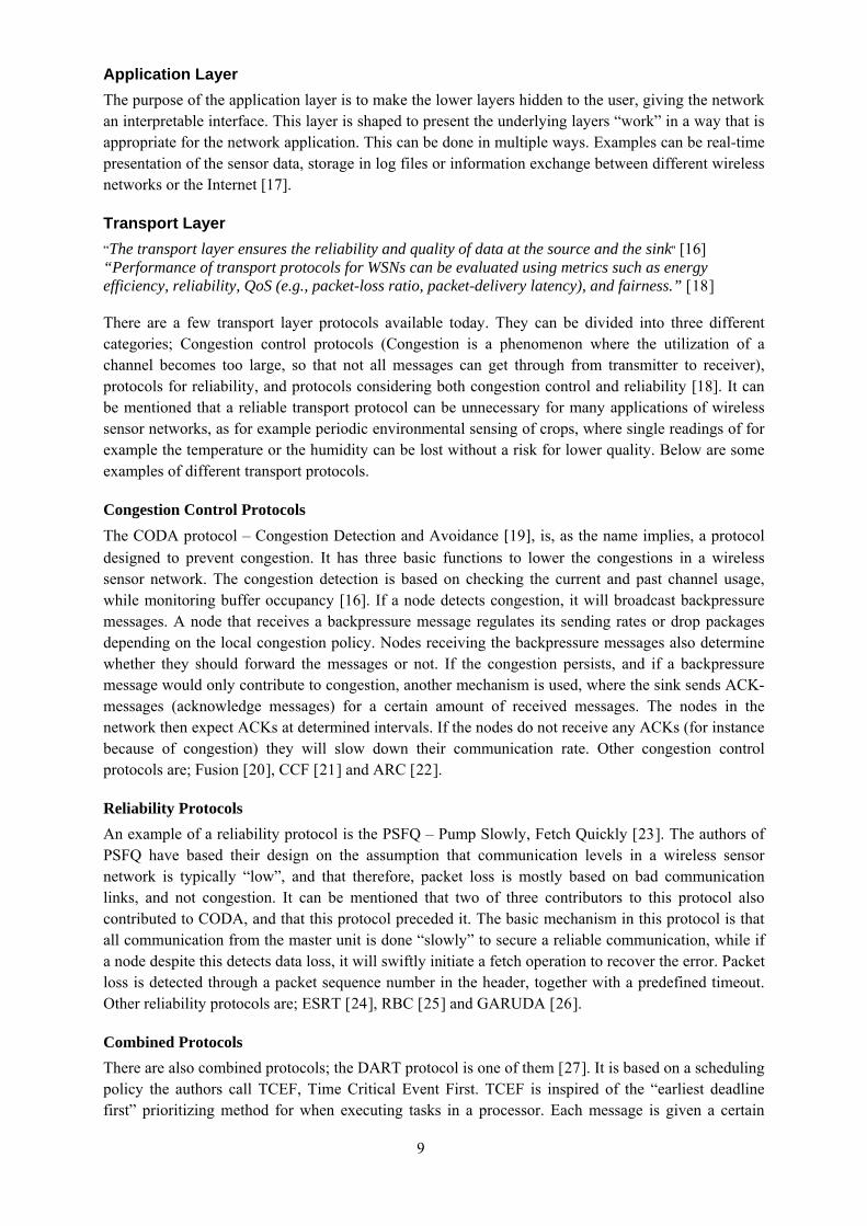
Application Layer The purpose of the application layer is to make the lower layers hidden to the user, giving the network an interpretable interface. This layer is shaped to present the underlying layers “work” in a way that is appropriate for the network application. This can be done in multiple ways. Examples can be real-time presentation of the sensor data, storage in log files or information exchange between different wireless networks or the Internet [17].
Transport Layer “The transport layer ensures the reliability and quality of data at the source and the sink” [16]
“Performance of transport protocols for WSNs can be evaluated using metrics such as energy efficiency, reliability, QoS (e.g., packet-loss ratio, packet-delivery latency), and fairness.” [18] There are a few transport layer protocols available today. They can be divided into three different categories; Congestion control protocols (Congestion is a phenomenon where the utilization of a channel becomes too large, so that not all messages can get through from transmitter to receiver), protocols for reliability, and protocols considering both congestion control and reliability [18]. It can be mentioned that a reliable transport protocol can be unnecessary for many applications of wireless sensor networks, as for example periodic environmental sensing of crops, where single readings of for example the temperature or the humidity can be lost without a risk for lower quality. Below are some examples of different transport protocols.
Congestion Control Protocols The CODA protocol – Congestion Detection and Avoidance [19], is, as the name implies, a protocol designed to prevent congestion. It has three basic functions to lower the congestions in a wireless sensor network. The congestion detection is based on checking the current and past channel usage, while monitoring buffer occupancy [16]. If a node detects congestion, it will broadcast backpressure messages. A node that receives a backpressure message regulates its sending rates or drop packages depending on the local congestion policy. Nodes receiving the backpressure messages also determine whether they should forward the messages or not. If the congestion persists, and if a backpressure message would only contribute to congestion, another mechanism is used, where the sink sends ACK-messages (acknowledge messages) for a certain amount of received messages. The nodes in the network then expect ACKs at determined intervals. If the nodes do not receive any ACKs (for instance because of congestion) they will slow down their communication rate. Other congestion control protocols are; Fusion [20], CCF [21] and ARC [22].
Reliability Protocols An example of a reliability protocol is the PSFQ – Pump Slowly, Fetch Quickly [23]. The authors of PSFQ have based their design on the assumption that communication levels in a wireless sensor network is typically “low”, and that therefore, packet loss is mostly based on bad communication links, and not congestion. It can be mentioned that two of three contributors to this protocol also contributed to CODA, and that this protocol preceded it. The basic mechanism in this protocol is that all communication from the master unit is done “slowly” to secure a reliable communication, while if a node despite this detects data loss, it will swiftly initiate a fetch operation to recover the error. Packet loss is detected through a packet sequence number in the header, together with a predefined timeout. Other reliability protocols are; ESRT [24], RBC [25] and GARUDA [26].
Combined Protocols There are also combined protocols; the DART protocol is one of them [27]. It is based on a scheduling policy the authors call TCEF, Time Critical Event First. TCEF is inspired of the “earliest deadline first” prioritizing method for when executing tasks in a processor. Each message is given a certain
9

deadline and a node will schedule its transmissions to best meet the deadlines. To prevent a global clock from being needed in the network, each node adds the “package-time” to the transmission. The congestion control is implemented at node level where each node checks its buffer levels and the average node transmission delay. The node transmission delay indicates how much traffic currently taking place. If congestion is detected, the node will set a congestion notification bit in the message header. The sink can then compute new update intervals from the nodes through checking message delays, and then broadcast the new intervals to the nodes. Other combined protocols are; PORT [28], DST [29] and STCP [30].
Network Layer The network layer is realised via a routing protocol. Routing techniques are tightly connected to logical network topology. The subject “routing” is very wide and the variety of different routing protocols is huge. The protocols can be divided and classified in different ways. One wireless mesh networks survey [17] divides them in four areas; Multi-radio routing, multi-path routing for load balancing and fault tolerance, hierarchical routing (clustering), and geographical routing. Other authors of routing articles [31,32] approach routing in a different way, dividing them into Pro-active and Re-active routing, and hybrids in between. Pro-active routing determines the routing paths in advance, before they are used, while re-active routing computes the routes at the time they are needed. Furthermore, the routing can be divided into; flat-based routing, hierarchical based routing and location-based routing, classified into multipath-based, query-based, negotiation-based, QoS-based (Quality of Service), and coherent-based routing techniques [31]. The two probably most prominent routing protocols in WSN context are LEACH – Low Energy Adaptive Clustering Hierarchy [33], and AODV– Ad hoc On demand Distant Vector Routing [34]. A good source when looking for other routing protocols is “Routing Techniques in Wireless Sensor Networks: a Survey” [31].
LEACH is, as the name states, a clustering routing protocol. It is self-organizing, and what makes LEACH special, is that it incorporates a mechanism for randomly rotating the cluster heads (the “base station” in the cluster). The cluster heads in a hierarchical network have a higher power consumption since they forward other nodes messages as well, and by rotating the task, the differences in power consumptions is levelled out. Each cluster also compress the sensor data (if data is the same etc) to lower the amount of data needed to send to the base station. In the cluster head shift phase, a CSMA (Carrier Sense Multiple Access) MAC is used and all nodes must have their receivers on. The cluster heads determines TDMA-schedules (Time Division Multiple Access) for their nodes to follow. The authors claim that a first node death will occur up to 8 times later than in a normal clustering hierarchy.
AODV has a totally different approach to routing. The authors call their proposal “a pure on-demand route acquisition system”. When a node wants to send data to a destination, it broadcasts a route request message. The receiving nodes rebroadcast the message as long as they are not the destination nodes. The destination node instead replies with a route reply message, and the route gets stored in tables in the nodes, and after that the discovered route is used. If a route is broken, decided by any node in the route, a new route request is broadcasted from the source node, if it still considers the connection being necessary. New nodes are discovered by them sending out “hello” messages. Nodes receiving these “hello” messages add the node ID to a table to include this neighbour. Because of the broadcasting nature of this protocol, it is neither energy efficient nor adapted to networks with low duty cycle radio transmissions.
10

Data Link Layer The data link layer consists of the MAC protocol, giving rules how the nodes can access the wireless medium. There are several different approaches to making a functional MAC protocol, and there are several MAC protocols specialized for use in wireless sensor networks.
Usually MAC protocols are designed to provide high data throughput and low latency [35], this does not apply on protocols for wireless sensor networks. Because of the wireless nature of the nodes, focus is laid on keeping power consumption low [16].
“…a good MAC protocol for the wireless sensor networks, considered the following attributes. The first is the energy efficiency. Another important attribute is the scalability to the change in network size, node density and topology. Some nodes may die over time; some new nodes may join later; some nodes may move to different locations. The network topology changes over time as well due to many reasons. A good MAC protocol should easily accommodate such network changes. Other important attributes include fairness, latency, throughput and bandwidth utilization.” [36] Depending on a networks application, the uses of certain MAC protocols are to be favoured. Some protocols are adapted to networks with many nodes and much or little data throughput, while others are adapted to smaller networks. There are mainly three different communications patterns MAC protocols are adapted to; “Local uni-/broadcast” [35,44], “nodes to sink report” [35,44] and “sink to node control dispatch” [44]. The use of ad hoc connectivity of nodes is also an aspect to consider. A network capable of ad hoc connection requires complex algorithms and much memory in each node, as well as higher power consumption.
Some of the problems MAC protocols designers consider are radio idle listening, collisions, protocol overhead and overhearing [35]. The biggest problem is considered being the idle listening, as it is a pure waste of energy [35,36]. This is because the radio circuit consumes large amounts of power when active. Synchronization-procedures are also necessary, since the microcontrollers oscillators drift relative each other and the nodes eventually get an offset in their conception of time, which impacts communication. Different protocols are more or less vulnerable to this phenomenon.
Modern WSN MAC protocols use mainly two different techniques, with some variants, for maintaining communications within the wireless sensor networks. These are “Low-power Listening” (LPL) and “Coordinate Sleep Schedules” (CSS) [35,36,37,38,39,40,41,42,44]. Low-power Listening is based on data transmissions with very long preamble and receivers who wake up in certain intervals to listen for preambles. The preamble is longer than the time span for the “sampling” of the radio medium, check interval, in which the nodes sleep, to ensure the receiver hears the preamble. Coordinate Sleep Schedules functions more like traditional TDMA, but with less strict timings due to the rather volatile characteristics of the communication sprung from the radio medium combined with separate drifting oscillators in each node. Naturally, LPL feels like a good choice for networks with very low activity, while CSS is less sensitive to the amount of traffic on the network.
A short introduction to a handful of MAC protocols present today is given below;
B-MAC – Berkeley MAC [37] This protocol utilizes Low-Power-Listening with eight different, eligible check intervals, combined with CSMA for effective collision avoidance [37]. The designers wanted to make the protocol as flexible as possible, giving it a very small core, with only link layer functionality. Other functionality is then added on top of the protocol, for instance RTS/CTS (Request To Send/Clear To Send) channel acquisition protocol or ACK-functionality [37] The B-MAC outperforms S-MAC [37,39] as well as T-MAC [39]. More on these two protocols further down.
11

WiseMAC - Wireless Sensor MAC [38] This is a protocol based on Low-Power Listening focusing on low-traffic networks. In WiseMAC, the access point/sink is the only initiator of communications. The trick to getting lower power consumption lies in that the access point learns the check intervals of the nodes, so it knows when to transmit data, and thereby lowering the need for a long preamble [38]. This is made possible via a modified ACK-package, also returning the time until the node next will sample the air for activity [39].
S-MAC – Sensor MAC [36,43] S-MAC applies coordinate sleep-schedules combined with RTS/CTS and message passing. In short, it functions as each node stores a table of its neighbours, creating sleeping schedules based on this table and then the nodes “find” appropriate sleeping schedules [36,44]. Each slot where a node is awake and active is 300 ms [44], and RTS/CTS is then used to exchange information between nodes [37]. As this solution requires that each node have a table of neighbouring nodes, it has an obvious limitation to how dense the network can be.
T-MAC – Timeout MAC [35] The authors of T-MAC compare it to S-MAC; they are somewhat similar, but with some modified functionality; variable/adaptive active time slots and FRTS, Future Request To Send. The protocol automatically adjust the nodes active timeslots based on how much data that will be sent. FRTS functions as if a node overhears a CTS signal, and have data to send but is not the one eligible to do it, it can transmit a FRTS, to let the receiving node know that it will have to extend its active time to receive data from the node transmitting the FRTS.
SCP-MAC – Scheduled Channel Polling MAC [39]
Scheduled Channel Polling MAC reminds mostly of a further iteration of Low-Power Listening, with scheduled polling of the radio medium. This shortens the preamble to a short “tone” to create a connection. This is established by scheduling data containing how a node plan to stay awake, added to the data packages, so a potential sender always know when the receiver will be active and polling for transmissions. SPC-MAC also uses two contention windows, one to check for activity before the “tone” and one to check for activity after the “tone”, before data can be sent.
SEA-MAC – Simple Energy Aware MAC [40] SEA-MAC’s authors have taken a slightly different approach than others when designing their MAC. It is based on a scenario where every node in the network only is active when it samples its sensors. All synchronization is started in the access point/base station, and then forwarded by nodes to lower levels in the network. This lowers energy consumption by nodes not having to poll the medium for transmissions, nor having to use tones or preambles. They only have to get synchronized when turned on, and every single node only uses one schedule.
Unnamed [42] The authors of SEA-MAC accompanied by two more people proposed an unnamed protocol in 2007. It uses a mechanism they call route partitioning, divided in two parts. Firstly an initialization phase, where nodes “speak freely” and report their existence, forwarded to the base unit. The base unit calculates the best routes for communications flow, and distribute the schedules to the nodes. Similar to SEA-MAC, the nodes only wake-up to sample data, which they add to the incoming data from other nodes, before forwarding to the base station. The schedules make sure only one route is active at a time.
Other MAC protocols are D-MAC [44], TRAMA [45], BMA [46], LMAC [47], Z-MAC [41], PAMAS [48], STEM [49], PMAC [50] and the very new ET-MAC [51].
12

Physical Layer “Communication between two nodes requires creating a physical link between two radios. The physical layer handles the communication across this physical link, which involves modulating and coding the data so that the intended receiver can optimally decode it in the presence of channel nonidealities and interference”[32]
The physical layer in a wireless sensor node has three aspects [6]; Cost of the physical component/components, power consumption of these components, and the regulations regarding the usage of different frequency bands in different countries. Another concern for the designer is how the signal is going to be modulated [16].
Typically, power consumption of a radio circuit and the transmission conditions are connected. Distance, frequency band and modulation, as well as interference of different kinds, all affect the power consumption [16]. A certain unit for measuring the performance of a physical layer has been proposed, the EPUB, Energy-Per-Useful-Bit [52].
The cost of a circuit can be easily influenced by how the designer chooses amongst different manufacturers. The manufacturers data sheets usually also gives good indications on how high power consumption the circuit has. What frequency bands the circuit utilizes impacts the power consumption of the circuit. Generally, a lower frequency leads to lower power consumption, but also a lower data transmission rate, so the time the radio circuit is transmitting is extended. Frequencies of common use are 433 MHz (EU), 868 (EU), 915 (US) and 2400 (ISM) MHz, and some modulation techniques used are PSK (Phase Shift Keying, for instance binary or quadrature), FSK (Frequency shift keying, for instance Gaussian or Binary) and ASK, Amplitude Shift Keying [6]. There are also several hybrid modulation techniques mixing the above methods.
2.4.3 Operating Systems The amount of scheduling potentially needed for the protocol of a wireless sensor network can be of great extent. Utilizing an operating system in the microcontroller is a way to lower the potential problems related to this scheduling. An operating system usually provides scheduling tools in addition to the basic timer functions of a microcontroller unit, making it possible to increase the dynamics and flexibility of the software. With an operating system, the option to use multiple threads of executing is also available. The possibility to use multi-threading further increases the software’s potential. Traditional code in a microcontroller is written as a single thread, where only interrupts change the flow of the program (when an interrupt occurs, the program counter is vectored to the interrupt vector, where it executes the interrupt routine before going back to the main program).
Two popular operating systems for wireless sensor networks are the TinyOS [53], and Contiki [54], the later developed by Swedish Adam Dunkels. These OS are extremely small to be able to fit into a microcontrollers flash memory, size typically in tenths of kilobytes [55], depending on functionality. The size of an operating system and the execution overhead associated with the scheduling are known drawbacks, and therefore, an evaluation should be done to determine whether an OS should be used or not. This is however considered being a part of F. Smitt’s thesis [1].
13
3 EXAMPLES OF PRESENT SOLUTIONS
3.1 Motes A mote is what could be considered as the physical hardware in the nodes. Wireless Sensor Networks are a fairly new technology, and a lot of research and development is being done across the world today. The online wiki SNM - The Sensor Network Museumtm [56] together with Tatiana Bokareva, PhD student at the School of Computer Science and Engineering, in Australia’s Mini Hardware Survey [57] and wikipedia.org [58] gives a good overview of the WSN mote-alternatives available today. These motes cannot be considered as COTS-alternatives (Commercial Of The Shelf) as they do not have any casing, they are designed for integration in product solutions. The majority of the motes mentioned there, and produced in the last years, are compliant with the ZigBee-standard. The most prominent motes, when searching the Internet, are those developed at Berkeley, University of California [59]. Their latest mote is called Telos. Telos is a complete solution with 802.15.4 compliance and onboard USB-connectivity and sensors. It has the size roughly as the battery pack of two AA-batteries. Telos is sold by Crossbow Technologies [60], a company specializing in sensors and now lately also in wireless sensor networks. Sentilla [61] (formerly known as moteIV) sells an, according to them, upgraded version of the Telos mote, called Tmote Sky. Another interesting contender is the low-cost Webee mote from Lucerne University of Applied Science. It mainly only has two disadvantages: The mote is very “naked” in the meaning that it has no other functionality than pure ZigBee and sleep-functionality. The other disadvantage is the antenna, it is an antenna specially adapted for use in Bluetooth headset units, where the human heads impact on the radio waves has been considered (it is adapted for frequencies 200 MHz higher than what ZigBee actually use). The pricing however is only €11,99 if 10000 motes are bought [62], compared to Crossbow’s Telos mote, which prising is set to $134 or $174 (with/without sensor suite) for customers in Europe [63]. Telos’ predecessor Mica2 has a cost of 1035 swedish kronor for between 10-24 units8. The Swedish agent for Crossbow Technologies is Amtele AB.
A comparison between a handful of motes is presented in Table 2. The pricing is somewhat inconsistent when it comes to quantities.
3.2 Zigbee, IEEE 802.15.4 Zigbee and IEEE 802.15.4 (a standard from Institute of Electrical and Electronics Engineers) together [64,65,66] form a standard for low-traffic wireless networks with requirements having low power consumption and being cheap. Zigbee is made up from the top layers of the communication stack, while the IEEE 802.15.4 defines the two lower layers, MAC- and physical layer. The Zigbee standard supports up to 65000 nodes, but in a master-node relationship, the master can only have 254 nodes. The absolute minimum hardware requirement for Zigbee is an 8-bit 4MHz microcontroller unit with 32kilobytes ROM (Read Only Memory) and 8kilobytes RAM (Random Access Memory). Zigbee utilizes cluster head rotation technique for levelling out the power consumption in the network, though these cluster heads are called mediation devices in Zigbee. Communication routes are established with AODV. IEEE 802.15.4 operates on three frequency bands; 868, 902-928, 2400-2483,5 MHz. The bit rate is dependent on what frequency band is used, 250kbps on the 2.4GHz band and 20kbps on the 868MHz band.
8 Price-offering from e-mail-correspondence with Crossbow/Amtele
14

Mote Sensors Radio band
MCU Power cons. sleep/-standby
Power cons. TX/RX active
PC-interface
Cost
Tmote Sky [67]
Humidity, light, temperature
2.4GHz MSP430 F1611
75,6 μW 82.8mW USB N/A9
Mica2 [68]
Available, off chip
868, 916 MHz
Atmega 128L
54μW [69]
117mW [69]
Off-chip base station
1035 SEK
Mulle [70]
Temperature, accelerometer
2.4GHz Renesas M16C/62
12 μW10 162.85mW Bluetooth €175
Sun SPOT [71]
Temperature, accelerometer, light
2.4GHz ARM920T + ATmega48
118 μW N/A USB €630 for 2 nodes + base station
WeBee [72]
N/A 2.4GHz 8051 MCU N/A N/A N/A €11,99
Table 2, examples of motes
3.3 Z-Wave Z-wave [73] is a wireless mesh network solution for home automation. Its basic function is to transmit control messages from a controller (a network can have several controllers) unit to one or more nodes of different uses in a home, for example lighting or movement detection. The nodes reply and/or execute different tasks depending on their functionality. The mesh-technology used in Z-wave is somewhat limited, as only certain nodes, called routing nodes, can forward messages to other nodes. These nodes store static routes to use when relaying messages, and they are required to always be “on”, which gives them a substantially shortened lifetime if they are battery driven. The maximum number of nodes in a Z-wave network is 232. The Z-wave solution utilizes a combined microcontroller and RF-circuit developed at Zensys [74]. Because of the nature and specialization of Z-wave (in-door use and communications always initiated in the controllers), it is not suited for the application in this thesis. Z-wave operates on different frequencies around the world. 868 MHz in Europe, and 900-921 MHz in other areas.
3.4 Complete Product Solutions There are currently a couple of solutions for monitoring indoor and outdoor environments, on the market and for research-purposes. Crossbow Technologies recently presented a total solution for monitoring crops of various kinds, called eKo [75].
eKo is a system for monitoring crops and wine yards etc. eKo incorporates wireless solar-powered nodes for connecting sensors, and a gateway enabling connectivity to the internet. Crossbow has made eKo reachable over the Internet, to provide freedom to the user. The eKo starter-kit is priced at $3359 for 3 wireless nodes, one radio base station and one gateway with a secure web interface [76, 77].
Commonwealth Scientific and Industrial Research Organisation, CSIRO, in Australia has also made a wireless sensor network based on their FLECK-family of wireless motes. According to their homepage [78] they have deployed their networks at two different locations at today’s date, one at
9 Sentilla has discontinued their line of Tmote Sky products (email reference) 10 The Mulle document does not give any clear information on the actual power consumption during sleep.
15

their laboratory in Brisbane, and one at a cattle farm in Belmont. CSIRO’s primary aim is to provide a tool for scientists and specialists, and not for the commercial farmer, as in the case with eKo.
Another wireless sensor network for environmental monitoring is SensiNet® from Sensicast Systems. Sensicast Systems’ SensiNet [79] solution has been out on the market since 2003. Sensicast offers different kinds of nodes depending on the planned usage of the system. The customer can get voltage sensors and input current monitors as well as temperature and humidity sensors. Sensicast focus mainly on information-intensive manufacturing processes [80].
Other actors on the market offering WSN-solutions are for example Honeywell, Siemens and Emerson. Honeywell uses technology from Crossbow; they have a partnership since 2006 [81]. Emerson offers a wide range of products, mainly based on 2.4Ghz and 900 MHz communications (IEEE 802.15.4) using the HART/WirelessHART-protocol, a standard approved by the IEC as recently as the 19th of September 2008 [82]. Emerson’s WSN solutions have their main fields of application in the process industry. One of the transmitters used Emerson’s solutions is the Rosmary Analytical Model 6081-P [83], they have a wide variety of wireless sensors though, for different applications.
3.5 Why Develop a New Solution? Fredrik Smitt and the writer of this report evaluated the present solutions found available on the market, and based on the specifications set up in the beginning of the thesis, the decision was to try and develop a totally new solution. See chapter 1.3 Requirement Specifications for the specifications. The available motes on the market was perceived as being either unnecessarily expensive or having too high a power consumption. Regarding the already complete or semi-complete solutions as eKo or Zigbee/802.15.4 (with the WeBee mote alternative), they are considered being fairly viable alternatives, but eKo being too expensive, and Zigbee/802.15.4 supposedly being a bit too complex and unnecessarily hard to implement for the application. Syntronic has also earlier been looking at Zigbee-solutions and considered them as too expensive alternatives for their applications [84]. It was estimated that it should be possible to design a “good-enough-solution” with lower cost and lower power consumption than the majority of the present alternatives on the market.
16

4 THEORY REGARDING PCB DESIGN
4.1 The IPC Standards “IPC Standards and Publications are designed to serve the public interest through eliminating misunderstandings between manufacturers and purchasers, facilitating interchangeability and improvement of products, and assisting the purchaser in selecting and obtaining with minimum delay the proper product for his particular need.”
With IPC’s many years of experience and knowledge, they have adapted these standards to simplify for both the manufacturer and the designer. They state that a standard should not contain anything that cannot be defended by data, and therefore one could assume that their standards are well established by empirical data and facts, and thereby do not violate any of the many basic rules applicable when developing a PCB. They have also shaped their standards to decrease the “time to market” for a product, focusing on the end product performance.
This makes appropriate IPC standards viable to apply when designing any PCB. The standards applicable when designing the PCB in this thesis are 2221A11 and 222211 [85,86]. IPC 2221 is a generic standard for designing printed circuit boards, with further six specializations for different types of circuit boards, where IPC 2222 mainly covers the physical properties and plastic deformation of rigid printed circuit boards, such as dielectric material and thickness, and drill hole characteristics.
IPC gives a number of aspects to consider when designing a PCB, these are;
• Environmental Conditions. How will the operational environment look like for the finished product, temperature, ventilation, vibrations etc.
• Maintainability/reparability. This incorporates component placement, circuit density and test points.
• Process allowances and limitations of manufacturing equipment. Conductor width and spacing, tolerances etc.
• Interfacing. Connectors, mounting holes and component placement. • Coating and marking requirements. • Will the product be assembled by hand or machine. • Board performance class; General electronic product, dedicated service electronic product, or
high reliability electronic product. • Materials selection, board material as well as conductor and plating materials. • ESD sensitivity.
Other aspects to consider before entering the PCB design stage are the end product requirements, and the number of PCB layers required, based on how many routes and vias will be needed, plus the presence of any high frequency signals.
Because of the wideness of the IPC standards, only the parts vital to this thesis have been considered. Parts of the standards related to the manufacturing process have been left out, as these tasks have been outsourced to Cogra and the component placement team in Sandviken.
11 They cost $93 and $80 for non-printable hardcopies on CD, with 50% discount given to members of IPC.
17

4.2 Choice of Material The material can be divided into two areas, dielectric and conducting material. The materials of the PCB are chosen based on the requirements of the product or prototype. Aspects to consider are; temperature, both for when soldering and later on also the operating temperature, electrical properties (for instance high speed signals need a dielectric with higher isolating properties), required mechanical strength and the density of the circuitry. The conductive pattern and the plating also have several purposes; Conduct electricity and electrical signals, act as a heat relief to components, and to prevent corrosion.
The different dielectrics can be divided into; Epoxies, Silicone Elastomers, Acrylics, Polyurethanes, Specialized acrylate-based adhesives, and other adhesives.
Some examples of dielectrics are; FR4 (Flame Retardant 4, the most common dielectric), multifunctional epoxy, high performance epoxy, bismalaimide triazine/epoxy, polyimide, cyanate ester. Table 3 shows a comparison between three dielectric materials. The dielectric constant is a measurement on how “good” the material is at storing electrical charge, relative to vacuum. Dielectric strength shows how high potential difference the material can withstand without breakdown. Breakdown is when the material starts to conduct despite its isolating characteristics.
Dielectric material FR4 Bismalaimide Triazine
Cyanate Ester
Dielectric constant εr 3.9 2.9 2.8 Electric strength (V/mm) 39.4 x 10³ 47.2 x 10³ 65 x 103
Table 3, comparison between some dielectric materials
The commonly used basic material for the conductive pattern on the PCB is copper, and depending on the manufacturing process and future use, different plating can be added. Gold plating can be used to give resistant board edge connectors as well as to protect underlying layers from oxidation. Gold can also be used as an etch-fluid resist. Nickel plating can optionally be placed under the gold plating to give extra hardness to the contacts. The nickel will then prevent the copper from diffusing into the gold, levelling the surface and giving less porous gold plating. Tin or a tin/lead alloy can be used as a etch resist instead of gold. It should be noted however that if the alloy contains more than 0.1% lead, it would not be RoHS-compliant, and the product it was used in would probably not be sellable in Europe.
4.3 Issues Connected to Layout There are several aspects to consider when designing a PCB. Limitations in manufacturing equipment and techniques give restrictions in how conductors and vias can be routed and placed on a PCB. Susceptibility to damage is another aspect, as well as electrical phenomena.
4.3.1 Manufacturing Aspects
Routing The viscosity of the etch fluid (etch fluid is used to remove copper from the parts of the PCB surface which is not wanted to be conductive) gives restrictions in how narrow the spacing can be between conductors on the PCB, and how sharp corners can be made in the routing. If spacing is too narrow or the corner is too sharp, the etch fluid will not be able to circulate efficiently in that area, and will not be able to completely remove the copper surface. This can lead to short circuits between conductors.
18

Conductor width is also a concern. A too narrow conductor will be very susceptible to damage when etching and mounting, as it simply has less copper “to spare” if any plastic deformation of the copper surface is made.
To ease the verification process of the circuit pattern, as well as giving a professional look, it is also common practice to route conductors in specific directions on different layers in the PCB.
When routing conductors from any components connector pad to a reference plane of any kind, for instance ground, it is also advisable to use a so called thermal relief or a fairly long conductor, to lower the amount of energy used when heating up the pad when soldering the component foot to the pad. If the energy is insufficient, there is a risk that small surface mounted components will let go of the pad and “rise up”, standing straight up from the PCB [87].
When making a prototype PCB it is also advisable to route as many test points as possible on conductors, to be able to measure voltage levels and signals during testing without having to touch the components’ legs.
Hole Size The minimum size of mounting holes and vias are of course restricted to how small a drill can be and still function as a drill. How narrow it can be made is also related to the depth of the hole. A 5:1 depth/width ratio is recommended. Under normal conditions, the absolute minimum can be considered being 0,2 mm diameter [88].
Board Size/Thickness The board size should be made as small as possible. Smaller boards are less susceptible to bending forces, and can also be considered being cheaper, as less material is used. Increased thickness gives stronger boards, but at a higher cost. “Standard” board thickness is between 0.8 mm to 2.4 mm, including copper layers. The most common thickness is 1.6 mm.
Component Placement When placing components it is important to consider how the components will be soldered to place. Components placed too close to each other can create difficulties during soldering, and will also make it harder to replace faulty components and rework any faulty routings. Making sure that no components are in the way for connectors is also important. To avoid misunderstandings and make any hand soldering of components more time efficient, it is also advisable to always mark any polarity of components on the components silkscreen, and try to keep a unified direction of the components with polarity.
4.3.2 Electrical and Physical Aspects
Routing and Component Placement Depending on design, component choices and requirements, the layout of the PCB can be of great importance to lower sensitivity to EMI, crosstalk, switching noise and transients in signals. IPC divides digital signals into 4 groups, depending on their susceptibility to error; Non-critical (data buses, address buses), Semi-critical (reset lines), Critical (clock lines) and Super-Critical (for example clocks for ADCs, Analogue Digital Converters). These classes determine how important it is to protect the signal lines from disturbances.
19
Crosstalk and EMI Aspects to consider when routing is line width, density (spacing), length and location of the signal lines. To avoid cross-talk between signal lines, the routing should be made as “airy” as possible, with as little parallel lines as possible. This contradicts the manufacturing aspect, where lines are said to go parallel for a more “professional look” and more lucid design. To protect extra sensitive signal lines, they can be routed on a layer between two ground planes. A signal line routed this way is called a stripline. The two ground planes will protect and contain the signal lines electrical and magnetic field lines, reducing EMI. Crosstalk between lines is also lowered with this technique. Presence of the ground planes will heighten the lines capacitance, while lowering the impedance, compared to a normal, outer layer line (microstrip). Striplines on the edge of the PCB board will have limited protection.
Temperature Line width impacts the temperature as well as the impedance and intrinsic capacitance of the conductor. If there are any requirements on max conductor temperature, the necessary line width and thickness can be determined with equation 1.
725.0 44,0maxmax )( ec TTk
IA−×
= [mil2] [1]
A is the necessary cross sectional area of the conductor [square mil], I is the current that will flow through the conductor [A], k is 0.048 for conductors at the outer layers, 0.024 for inner layers. Tcmax is the maximum safe operating temperature of the dielectric material in the PCB and Temax is the highest temperature the environment will attain in where the PCB will be operated [oC].
Intrinsic capacitance The impedance and intrinsic capacitance of a conductor can be calculated with equations 2,3,4 and 5. The two first equations are valid for outer layer conductors (microstrips), while the two latter ones are valid for conductors placed equidistantly between two ground planes (striplines), with a line width at least 2 times greater than the distance to one of the ground planes.
⎥⎦⎤
⎢⎣⎡
++=
twhZ
r 8.098.5ln
41,187
0 ε[Ohm] [2]
00 Z
cCrε
= [pF/inch] [3]
( )
r
twtH
Zε
⎥⎦⎤
⎢⎣⎡
++
= 8.029,1ln60
0 [Ohm] [4]
⎥⎦⎤
⎢⎣⎡
+
=
twH
C r
8.081.3ln
41,10
ε[pF/inch] [5]
20

Z0 is the impedance, C0 is the intrinsic capacitance, c is the speed of light, h is the dielectric thickness, w is the line width, t is the line thickness, εr is the relative permittivity of the dielectric and H is the distance between the stripline and one of the ground planes.
Intrinsic inductance Any conductor also has an intrinsic inductance; this inductance makes the conductor store a small amount of energy from the magnetic field induced by the current. This causes transients and switching noise in circuits utilizing higher frequency signals. To reduce transients, the power-ground loop should be minimized, and to reduce switching noise, decoupling capacitors have been used for decades [89]. (Making sure the power to ground loop area is small is also important, as it will function as an antenna. Minimizing the area minimizes the sensitivity to interference). There are various techniques for decoupling. The most common one is to place capacitors as close as possible to the power supply pins of each IC on the PCB. This technique works fine in circuits using frequencies up to 50 MHz [90]. Above that, it can be necessary to place other similar capacitors across the PCB and also utilizing distributed interplanar capacitance between a ground plane and a power plane [90].
Grouping Regarding component placement, it is recommended to place components in “groups” related to each other. Analogue and digital parts separated, and higher frequency digital parts placed closer to the board power supply. This will minimize their impact on the other groups. Separate ground planes can be utilized for different groups, as long as any signal lines are not connected between the groups. If that is the case, the return current path of the signal will be made unnecessarily long. By placing a capacitor between the ground planes in the immediate vicinity of the signal crossing, the problem can be mitigated, but it is still not recommended.
Hole Size Via holes increase the parasitic inductance in a circuit, it is therefore advisable to use as few vias as possible. The parasitic inductance is also related to the hole size and the pad size surrounding the hole. A smaller hole and pad size gives a smaller parasitic inductance.
Filterbalun [91] The filterbalun and matching network of a transceiver circuit serves many purposes related to the characteristics and functionality of the transceiver. Component choices and placement as well as conductor width and shape can give noticeable changes in the behaviour and quality of the radio communication. The main points when designing a balun can be summarized into a short list;
• Filter higher radio frequencies received by the antenna • Match the impedance of the transceiver pins with the antenna for high sensitivity during receiving,
and low power consumption during transmission. • Convert signals from balanced signals (at the transceiver IC) to unbalanced signals (at the
antenna), or vice versa. • Lower spurious emissions and harmonics, to fulfil any regulations regarding this. The filterbalun need to be adapted to the type of transceiver. Depending on model, the transceivers have different optimum output impedance, which then needs to be matched to 50 Ω at the antenna. The power consumption of a transceiver in TX-mode can be influenced by having different harmonics of the signal reflect back to the IC.
21

5 RADIO FREQUENCY REGULATIONS Swedish law defines a radio wave as an electromagnetic wave with a frequency between 9 kHz and 3000 GHz [92]. This spectrum of radiofrequencies is divided into radio bands, which have regulations regarding the usage of them. The regulations differ in the world depending on where you are located. Because of these differences in regulations, only the Swedish PTS (Post & Telestyrelsen) and European ETSI (European Telecommunications Standards Institute) have been considered in this thesis. They are to a large extent based on the worldwide ITU (International Telecommunications Union) standards for radio communications.
Usage of a frequency band usually requires a permit. There are, however, exceptions to this liability when using UWB (Ultra Wide Band) radio transmitters, as long as the transmitter output radiated power does not exceed some certain values12 [93]. Table 4 shows frequency bands between 0-1GHz dedicated for generic use [94,95]. 2,4 GHz - 2,4835 GHz can also be utilized in addition to these frequencies as long as the transmitter output power is below 100mW [96]. The later frequency band is part of the ISM-bands (certain frequency bands useable for Industrial, Scientific and Medical purposes), and it is accepted as a free to use frequency band all over the world, as long as the transmit power limit regulation is not violated.
Frequencies (MHz) Max duty cycle related to radiated power
Max carrier signal radiated power, ERP
Channel spacing
26,957 - 27,283 <10mW No specific 40,660 - 40,700 <10mW No specific
138,200 - 138,450 ≤ 1% <10mW No specific 433,050 – 434,790 ≤ 10% @ < 10mW or
≤ 100% @ ≤ 1mW No specific
863,000 – 870,000 ≤ 0.1% or LBT + AFA <25mW 25, 50, 100, 200 kHz 868,000 – 868,600 ≤ 1% or LBT + AFA <25mW No specific 868,700 – 869,200 ≤ 0.1% or LBT + AFA <25mW No specific 869,400 – 869,650 ≤ 10% or LBT + AFA <500mW ≤ 25kHz for 1 or
more channels 869,700 – 870,000 No restriction <5mW No specific
Table 4, Frequency bands between 0-1 GHz for generic use
12 0-1,6 GHz: EIRP (Equivalent Isotropically Radiated Power) = -90 dBm/MHz, peak isotropically radiated power = -50dBm/50MHz 1,6-3,4GHz: EIRP = -85dBm/Mhz, peak isotropically radiated power = -45dBm/50Mhz These values are valid when measuring with 1MHz bandwidth and an integration time of 1 ms. The peak isotropical radiated power is determined with a bandwith of 50MHz. If a narrower bandwidth of x MHz is used, the value should be reduced by 20log(50/x) dB[93].
22
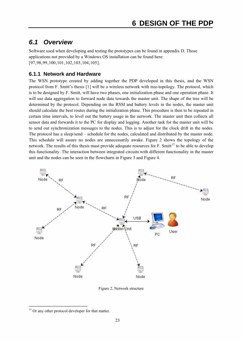
6 DESIGN OF THE PDP
6.1 Overview Software used when developing and testing the prototypes can be found in appendix D. Those applications not provided by a Windows OS installation can be found here: [97,98,99,100,101,102,103,104,105].
6.1.1 Network and Hardware The WSN prototype created by adding together the PDP developed in this thesis, and the WSN protocol from F. Smitt’s thesis [1] will be a wireless network with tree-topology. The protocol, which is to be designed by F. Smitt, will have two phases, one initialization phase and one operation phase. It will use data aggregation to forward node data towards the master unit. The shape of the tree will be determined by the protocol. Depending on the RSSI and battery levels in the nodes, the master unit should calculate the best routes during the initialization phase. This procedure is then to be repeated in certain time intervals, to level out the battery usage in the network. The master unit then collects all sensor data and forwards it to the PC for display and logging. Another task for the master unit will be to send out synchronization messages to the nodes. This is to adjust for the clock drift in the nodes. The protocol has a sleep/send – schedule for the nodes, calculated and distributed by the master node. This schedule will assure no nodes are unnecessarily awake. Figure 2 shows the topology of the network. The results of this thesis must provide adequate resources for F. Smitt13 to be able to develop this functionality. The interaction between integrated circuits with different functionality in the master unit and the nodes can be seen in the flowcharts in Figure 3 and Figure 4.
RF
Figure 2, Network structure
13 Or any other protocol developer for that matter.
23

Figure 3, The master unit
Figure 4, The nodes
6.1.2 Software
MCU The MCU software in this thesis is delimited to abstract the configuration and register settings portion of programming the MCU, so the protocol developer can concentrate on the protocol design and programming.
PC The main purpose of the PC software is to present sensor data from the network. This is accomplished by storing valid sensor data in a log file together with sensor ID, time stamp and battery status. The data is then presented in a table in the program. The software graphical interface and the code structure is also prepared for any protocol related code blocks that might be necessary to execute on the PC because of limitations in the microcontroller of the master unit.
6.2 Hardware
6.2.1 Choosing Hardware
6.2.1.1 MCU The microcontroller unit is the core of both the nodes and the master unit. It coordinates the data flow and execution chain, and can give a time perception to the system. Without an MCU or any similar IC it wouldn’t be possible to give the system the flexibility and dynamics needed to configure, control and maintain a wireless sensor network.
24

Specifying and Choosing the MCU When choosing an MCU, there are several properties to consider, depending on the application. For microcontrollers in wireless sensor networks, the most significant ones are;
- Power consumption and VCC range. Because of the wireless nature of the nodes, the power consumption should be as low as possible.
- Sleep modes. To further lower the power consumption, it is favourable to let the microcontroller enter a semi-functional state where it consumes even less power, without turning it of.
- I/O-ports + supported communication methods (SPI/UART etc). - Size of RAM/ROM. The protocol software will require a certain amount of RAM and ROM to
function. The chosen MCU should without doubt be able to handle the protocol software developed by F. Smitt. (“Enough, but less than ZigBee”). As it is a prototype it is better to go with “too much” RAM and ROM instead of risking having to little.
- Price. The price should be as low as possible to keep the cost of the PDP hardware low. - Performance can also be of importance, since faster execution should mean a shorter active
time. This aspect can be considered a minor problem though since the radio circuit will be the most time consuming circuit.
Since this is a master thesis, giving a limited amount of time for development, some other aspects also come in to consideration:
- Experience of the MCU from before. - Available expertise from employees at Syntronic AB and the tutor at KTH. - Software Development Environment/Kit.
Most of the motes developed the last couple of years has been using either a MSP430 from Texas Instruments, or an ATmega128 from Atmel [106]. For the shortest possible development time, a MCU from ATMEL is used. Syntronic AB’s employees are experienced on the ATmega-series of microcontrollers, and the software development tools are free of charge. A comparison between different microcontrollers available from Farnell is done in Table 5.
ATMEGA64L-8MU [107]
ATmega128L-8AU [108]
ATmega645V-8AU [109]
ATmega1281-16AU [110]
MSP430f156 [111]
Power cons. / VCC range
N/A 2.7-5.5 V
5.5 mA @ 4Mhz/3V 2.7-5.5 V
0.55mA @ 1Mhz/2V 1.8-5.5V
14mA @ 8Mhz/5V 2.7-5.5V
0.33mA @ 1Mhz/2.2V 1.8-3.6V
Sleep modes
ADC noise reduction, power save, power down, idle, stand-by, extended stand-by.
ADC noise reduction, power save, power down, idle, stand-by, extended stand-by.
ADC noise reduction, power save, power down, idle, stand-by.
ADC noise reduction, power save, power down, idle, stand-by, extended stand-by.
Five “low-power modes”
RAM/ROM 64KB Flash 2KB EEPROM 4KB SRAM
128KB Flash 4KB EEPROM 4KB SRAM
64KB Flash 2KB EEPROM 4KB SRAM
128KB Flash 4KB EEPROM 8KB SRAM
24KB+256KB Flash 1KB RAM
Price 91,97 SEK 208,27 SEK 99,13 SEK 118,48 SEK 146,12 SEK Experience Intermediate Intermediate Intermediate Intermediate None
Table 5, comparison of microcontrollers
25

The ATmega645V-8AU [109] The Atmega645V-8AU was considered the best alternative for the solution in this thesis. It has low power consumption, is fairly cheap and has the necessary functionality. Its functionality for having an external crystal oscillator to control one of its timers is optimized for low frequency crystals (quartz crystals, 32768 Hz), making it able to sleep for up to almost 8 seconds without waking up, using maximum prescaler. The VCC range where it can function at as low as 1.8V is also beneficial, as battery voltage level will drop with age, and two serial alkaline 1.5V batteries will “quickly” go lower than 2.7V. For high reliability during runtime it has a watchdog timer and brown out detection. A drawback with this MCU is that it might be unnecessarily powerful for the nodes in the network while it is not powerful enough for the master unit. Smitt’s thesis [1] will show.
6.2.1.2 Interface to the PC – The FT232R As the WSN prototype will have a connection to a PC, it is also necessary to somehow forward information from the WSN to the PC. A common method for doing this is with UART/RS232 communication via the PC’s serial port. Today, however, it is getting more and more common that computers do not come equipped with serial ports, they simply have USB-ports instead. The master unit should therefore be connected to the PC via USB. Writing drivers to USB is considered being complicated; therefore the company FTDI has created a series of USB converter ICs, capable of converting different communication standards to USB, while providing Windows-drivers enabling the converter to act like a serial port.
The chosen microcontroller ATmega645V-8AU provides functionality for communicating via UART/USART, SPI and I2C. The FTDI FT232R functions as a converter from UART to USB1.1/2.0 and is a suitable choice of IC for giving the PDP’s master unit USB connectivity. It has a built in voltage regulator to convert the 5V USB supply voltage to a lower 3.3V. This simplifies the design of the printed circuit board, as the chosen transceiver circuits max supply voltage is 3.9V. Other beneficial functions with the FT232R are handshake signals for the UART communication and LED indication for active communication. The handshake signals can be used to control how often the chip forwards data packets via USB, and also to ensure that no data is sent to the chip while its buffer is full.
The FT232R with the best pinout-option was determined to be the FT232RL [112].
6.2.1.3 The CC1101 [113] What transceiver circuit and antenna to employ was determined by F. Smitt in [1] and provided to the writer of this report. The CC1101 is a very cheap and competent transceiver circuit with many options and functionalities for the protocol software designer to utilize. It has good sensitivity and fast initialization times and switching times between modes, which shortens the time the transceiver uses power without being functional. This is a great advantage over many other transceivers (for instance the nRF905), since the time slots the nodes will have to be active can be made much shorter. It has a wide range of extra functionality beneficial for the designer of the protocol. Another beneficial function is the whitening of the data transmitted. Data transmitted is XOR-ed with a PN9-sequence, to give the data a more balanced send pattern of 1’s and 0’s transmitted. A de-whitener is required in the receiver to interpret the data. In addition to all this, Texas Instruments provide a reference design of the filterbalun, guaranteed to fulfil ETSI regulations regarding spurious emissions. Frequency ranges of the circuit are; 300-348 MHz, 387-464 MHz and 779-928 MHz.
A ¼-whip SMA-connected antenna was also provided. See F. Smitt’s thesis report for more information [1].
26

6.2.2 Hardware Design To make the PCB design as quick and cheap as possible, the master and node PCBs was integrated into a single design. The components mounted on the PCBs then determined the functionality of the circuit board. The time for routing was thereby shortened, and the manufacturing costs of the PCBs was also expected to be lower than if two different PCBs were to be manufactured.
As with any other PCB design, a schematic was made before PCB layout, showing all necessary connections and components. The schematic was then used to make the PCB layout. Because of the nature of the PCB, where master and node share the same layout, the schematic shows a hybrid master-node. The schematics can be found in appendix B.
A 4 layer PCB was made, with a stack-up as in Figure 5. It is probable that a two-layered design could have been used, however it is easier to route a 4-layered board and therefore this was preferred. You also get separate ground and power planes which can be considered good effects of this choice. The top layer has in addition to the conductive copper layer also a pastemask, soldermask and a silkscreen, for easier mounting of the components. Appendix C shows the copper patterns of the different layers and the silkscreen. The manufacturing was first meant to be done in China for lower manufacturing cost, however the delivery cost would exceed this reduction in cost, and so the circuit boards were instead manufactured at Cogra Pro AB in Sweden.
Primary routing layer. 0,035mmFR4 dielectric. 0,23 mmGround plane. 0,017mmFR4 dielectric. 1,036 mmPower plane. 0,017mm
Secondary routing layer. 0,035mmFR4 dielectric. 0,23 mm
Figure 5, PCB layer stack-up
The primary design characteristics of the PCB are;
• The top layer acts as primary signal routing layer. • Grounded copper fill on the top layer, with vias connecting to the ground plane below. • Pin-headers for connection to external sensors and programming devices, as well as any future
expansion cards. • Multiple test-points for testing purposes as well as for any future modifications. • Divided VCC-plane. The transceiver has a separate VCC-plane in the power-layer, connected to
the other plane with a ferrite bead and a capacitor. This is in accordance with reference design provided from Texas Instruments.
• Powered circuits have been placed in a way so any return currents to the power supply should have a small impact on sensitive circuits’ performances.
• Vias have been designed as through-hole to make for cheap manufacturing, and has to the greatest extent been placed to minimize any impact from parasitic inductance.
• Thermal relieves have been placed around vias, to lower the amount of thermal energy dissipated from component pads when preheating them before soldering.
• Trace thickness and width have been adapted for a microstrip impedance in the balun close to 50Ω, see Figure 6. The impedance was calculated with the software RFsim99.
27

• Facing the radio balun away from the rest of the circuits lowers any interference from USB/UART/SPI communication. The design of the balun was made in accordance with reference designs provided by Texas Instruments.
• Crystal oscillators have been placed as close to the circuits as possible. • Decoupling of the VCC to the circuits has been made, in accordance with the reference designs
provided by the manufacturers. • No conductor corner angles are narrower than 90o, and everywhere possible, they have been
routed as 45 o. • FR4, Flame Retardant 4, is used as dielectric material between layers. • 10kΩ pull-up resistors have been used where necessary. • Jumper to choose JTAG power supply or battery power supply while programming the MCU via
the JTAG debugger. • The FTDI-chip is configured and routed as a USB 1.1 device, to be connectable to older PCs. • A low-power 32.768 kHz crystal oscillator is employed to enable MCU sleep and timer-based
wake-up on interrupt. • To enable measuring battery voltage level in the nodes, a conductor was routed to an ADC port,
passing a 1/3 voltage divider. With the internal 1.1 V reference voltage it is possible to read battery voltages below 3.3V.
Employees at Syntronic Kista reviewed all work14. Mounting of components on one master unit and two nodes were done at Syntronic Gävle. Magnus Söderlind and the writer of this report soldered one additional master unit at the Kista office. To enable extra functionality in the transceiver, two smaller modifications were made on the finished PCB. Pins GDO0 and GD02 on the transceiver was connected to pins PINB6 and PINB7 on the MCU to enable external interrupts from GDO0 and GDO2. A faulty routing of the CTS# between the ATmega and the FT232R was also discovered during the testing of the hardware. It was corrected on the concerned circuit boards in the Syntronic Kista Electronics lab. Because of the four-layer design, the distance between the ground plane and the radio balun differ from that of the reference design. This should only impact the impedance matching.
Thickness: 0,035mm
Balun conductor width: 0,3mm
Spacing: min. 0,2mmWidth: min. 0,2mm
Figure 6, Conductor width, thickness and spacing.
14 Schematic reviewed by Magnus Söderlind, Carl-Johan Ohlson, Johan Waldebäck. Component choices reviewed by Magnus Söderlind. PCB design reviewed by Magnus Söderlind and Carl-Johan Ohlson.
28

6.3 Software
6.3.1 Choosing Programming Language and IDE An integrated development environment, IDE, is an application that unifies most parts related to developing software. It can comprise a code editor, a compiler and a debugger, easily utilized through its’ user interface. In this thesis, two IDEs must be chosen, one for developing the MCU software, and one for developing the PC software.
ATMEL provides free IDE software for developing C/C++ code to their microcontroller units. The graphical PC-software development leaves more options since there are various programming languages available to create graphical applications in. There are a couple of aspects to consider when choosing, since it is a master’s thesis, giving limited resources and time;
• Easiness in use • Price for using the IDE • Earlier experience • Possible support from employees and KTH supervisor. Based on these aspects, C#.NET was chosen as the best language and environment to develop the graphical application in. Syntronic already has license for using Visual Studio 2005 with the .NET framework, and many employees got experience from programming in the IDE, implying good support if problems would arise. The programming language C# was chosen on the basis of it being more similar to C/C++ than any other language used with .NET.
6.3.2 Software Design
6.3.2.1 MCU Software The functionality of the MCU software written in this thesis was delimited to what closely could be called abstraction layer type functions and initialization functions, for the protocol developer to use when designing the communication protocol software. This incorporates setting configuration registers and preparing interrupt service routines. As node and master functionality differs, they have different sets of functions and settings.
Master Functions • Pin direction settings • Power management configuration • Initialization and configuration of peripherals • Timer handling functions • UART communication functions • Probable useful interrupt service routines (UART received, Timer overflow)
Node Functions • Pin direction settings • Power management configuration • Initialization and configuration of peripherals • Timer handling functions • ADC handling functions • Probable useful interrupt service routines (ADC conversion complete, Timer overflow)
29

6.3.2.2 PC Software The application designed in this thesis, a part of the PDP and also to the future WSN prototype, is named Sensor Mesh GUI. It is a graphical application providing a clear and fairly intuitive control panel for managing the network and retrieving and presenting logged data from it, saved in a log file at a location of choice. It is prepared for future application specific modifications, and has empty code blocks and user interface-buttons reserved for any network protocol related programming, if the protocol designer would need the calculating power of the PC for determining routes or similar tasks.
The Interface The Interface of Sensor Mesh GUI is divided into three different tabs; Basic user, Advanced user, and Application specific settings. The Application specific settings tab is reserved for future functionality, and comprises only examples of what functionality could be implemented in the network and the Sensor Mesh GUI. The application specific tab is shown in Figure 10.
Basic User Tab The basic user tab presents sensor data from the WSN. It gives the user the option to show the latest reading from every node in the network, or all readings from any specific node. It also shows the status of the WSN and if the COM port is active. If the history of a specific node is of interest, clicking on the radio button “node history” will bring up a pop-up window showing all node IDs that have been logged so far. A node of interest is chosen and clicking “OK” dismisses the pop-up. Figure 7 and Figure 8 shows examples of the appearance. Faked sensor data is shown in these two pictures, used for when debugging the application.
Figure 7, Basic user tab
30
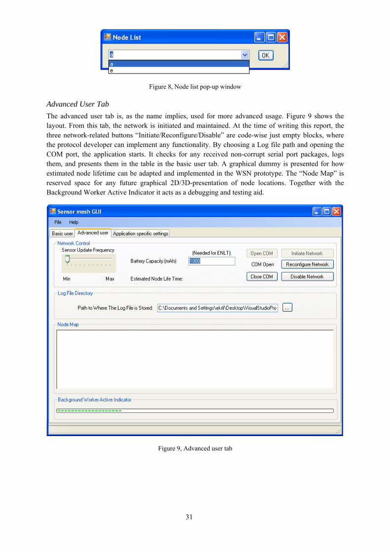
Figure 8, Node list pop-up window
Advanced User Tab The advanced user tab is, as the name implies, used for more advanced usage. Figure 9 shows the layout. From this tab, the network is initiated and maintained. At the time of writing this report, the three network-related buttons “Initiate/Reconfigure/Disable” are code-wise just empty blocks, where the protocol developer can implement any functionality. By choosing a Log file path and opening the COM port, the application starts. It checks for any received non-corrupt serial port packages, logs them, and presents them in the table in the basic user tab. A graphical dummy is presented for how estimated node lifetime can be adapted and implemented in the WSN prototype. The “Node Map” is reserved space for any future graphical 2D/3D-presentation of node locations. Together with the Background Worker Active Indicator it acts as a debugging and testing aid.
Figure 9, Advanced user tab
31
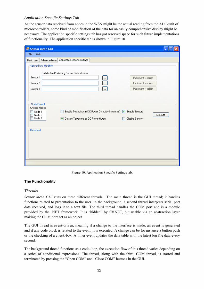
Application Specific Settings Tab As the sensor data received from nodes in the WSN might be the actual reading from the ADC-unit of microcontrollers, some kind of modification of the data for an easily comprehensive display might be necessary. The application specific settings tab has got reserved space for such future implementations of functionality. The application specific tab is shown in Figure 10.
Figure 10, Application Specific Settings tab.
The Functionality
Threads Sensor Mesh GUI runs on three different threads. The main thread is the GUI thread; it handles functions related to presentation to the user. In the background, a second thread interprets serial port data received, and logs it to a text file. The third thread handles the COM port and is a module provided by the .NET framework. It is “hidden” by C#.NET, but usable via an abstraction layer making the COM port act as an object.
The GUI thread is event-driven, meaning if a change to the interface is made, an event is generated and if any code block is related to the event, it is executed. A change can be for instance a button push or the checking of a check-box. A timer event updates the data table with the latest log file data every second.
The background thread functions as a code-loop, the execution flow of this thread varies depending on a series of conditional expressions. The thread, along with the third, COM thread, is started and terminated by pressing the “Open COM” and “Close COM” buttons in the GUI.
32
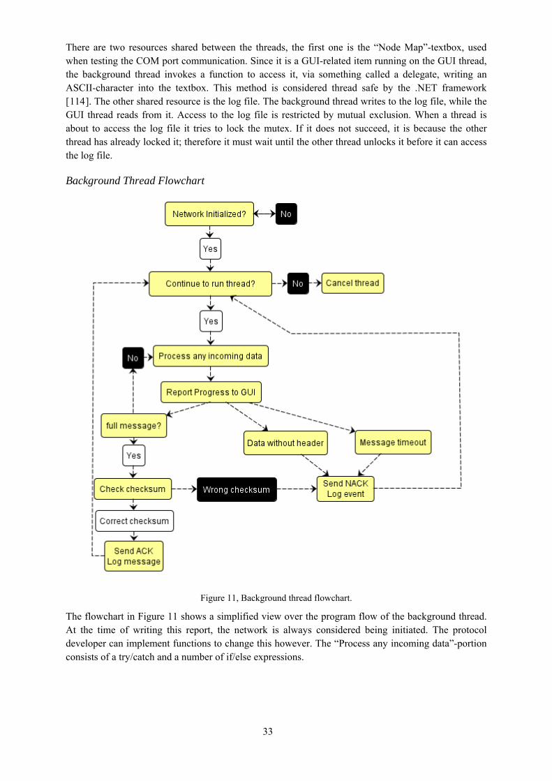
There are two resources shared between the threads, the first one is the “Node Map”-textbox, used when testing the COM port communication. Since it is a GUI-related item running on the GUI thread, the background thread invokes a function to access it, via something called a delegate, writing an ASCII-character into the textbox. This method is considered thread safe by the .NET framework [114]. The other shared resource is the log file. The background thread writes to the log file, while the GUI thread reads from it. Access to the log file is restricted by mutual exclusion. When a thread is about to access the log file it tries to lock the mutex. If it does not succeed, it is because the other thread has already locked it; therefore it must wait until the other thread unlocks it before it can access the log file.
Background Thread Flowchart
Figure 11, Background thread flowchart.
The flowchart in Figure 11 shows a simplified view over the program flow of the background thread. At the time of writing this report, the network is always considered being initiated. The protocol developer can implement functions to change this however. The “Process any incoming data”-portion consists of a try/catch and a number of if/else expressions.
33

Data Table Display Functionality Flowchart
Figure 12, Data table display functionality flowchart
Every second, the GUI thread refresh the data table displaying the sensor node data fetched so far and logged in the log file. The “Node History” display option in the GUI is not made available before the Node ID List has been created and fully updated by the “Latest Readings”. Figure 12 shows the flowchart.
Serial Port Communication To make the forwarding of sensor data from the WSN to the PC error free, all communication carrying such information is preceded by a header byte, and the last byte also contains checksum-like information. Any information exchanged during network initialization or reconfiguration will not necessarily be required to follow this pattern, since it is the area of the protocol designer. A sensor data packet is comprised of eight bytes. Figure 13 shows the packet structure. The checksum byte is created by adding together the value of all data bytes (node ID, battery level, sensor data and network level) and dividing them by the packet length. Only one byte is reserved per ADC value, while the ADC outputs a 10 bit value. The effect of this is a lower resolution of the values sampled.
Figure 13, Sensor data packet structure
34

Logged Data Correct sensor data packets are stored in the log file with a time stamp as hh:mm:ss yyyy-mm-dd. Erroneous communication is also logged. If the checksum of a full received message is wrong, “checksum error” will be logged. If communication timed out, “serial com. timed out” will be logged, and if data without a header was received, “got data w/o header” will be logged. All logging is done on a new row. Figure 14 shows an example of the log file. At the time the writer of the report called the checksum error a “CRC error” (Cyclic Redundancy Check) with the ambition of making a more advanced error check. To make a lucid example, only standard ASCII-characters have been used when stating the example. In the first successful log, “d” is the header byte, “a” is the node ID, followed by the battery level “n” and three sensor data bytes “i” “e” and “l”. The network level is “s” and the checksum is comfortably enough, in this case, a simple “O”.
Figure 14, Log file example
35

7 RESULTS
7.1 Functionality All separate IC’s on the master unit and the nodes are functioning. SPI, UART, Sensor-enable signal, 32.768 kHz external crystal oscillator and AD-converters have been tested. See test reports (1-10) in appendix E.
7.1.2 Accuracy in Crystal Oscillator Frequencies The theory study on wireless sensor network protocols gave the insight that the TX/RX and awake/sleep scheduling is of extreme importance to the power consumption of the network. A tighter scheduling with better timing can cut of several percents of the consumption. Therefore it is important that the external oscillator crystal frequency does not deviate from the expected, as it is meant to be used as a timer input. Figure 15 shows the 32.768 kHz oscillator crystals frequency. The low number of digits provided by the oscilloscope however gives an insecure result. The result of 32.8 kHz cannot really tell how accurate the crystal is, only that it is not very inaccurate as in several percent error. It was discovered that when the MCU enters or exits power savings mode, there is a disturbance on the oscillator signal. The amplitude of the oscillation rises significantly. The reason for this is unknown at the time of writing this report. The anomaly has not yet given any impact on the predictability of the crystal. Figure 16 shows the anomaly as thin peaks. The MCU was programmed to go to power save immediately after waking up15, running in a while(1)-loop, hence giving the periodical anomaly. See test reports (13,14) in appendix E for more information on the performing of the tests.
Figure 15, 32.768kHz crystal oscillations 15 From a timer compare match Interrupt. The Atmega645’s timer2 module is active during power-save mode.
36

Figure 16, Anomalies in amplitude from the 32.768kHz crystal, seen as thin peaks.
Similarly to the importance of having an accurate low-power oscillator crystal to use for time scheduling in the MCU, the transceiver also requires an accurate oscillator crystal for error free functionality. The minimum and maximum crystal oscillator frequency to the transceiver is 26 MHz and 27 MHz respectively [113]. Figure 17 shows the 26 MHz crystals frequency. It is slightly lower than 26Mhz, only 25,91 MHz. Given only two significant digits however, this would be rounded to 26 MHz. To heighten the frequency, a lighter load capacitance can be used.
It should be noted that the oscilloscope probes might influence the frequencies of these crystals as well. The lower oscillator crystal frequency has not given any noticeable impact on the functionality of the transceiver.
7.1.3 Transmit Frequency Spectrum The characteristics of the transmit frequency spectrum is also of importance. If the PCB design is bad, the conversion from balanced square signals at the transceiver outputs to an unbalanced sine wave at the antenna might be unsuccessful. The frequency band used by the protocol developed in F. Smitt’s parallel thesis employs the 868-868.6 MHz band and GFSK (Gaussian Frequency Shift Keying) modulation. Figure 18 shows a frequency spectrum visualization of a continuously transmitted preamble, test report (11) in appendix E. The peak frequency is at 868.29 MHz, close to the center frequency of the band. The picture shows an “average” signal where both the zeros and the ones in the preamble can be seen. This is because the oscilloscope is too “slow” to detect individual data bits, and therefore shows an average value. The frequency differences between the peaks in the picture are 20kHz (called deviation in the datasheet) and the total bandwidth-usage is slightly higher than 125kHz. (It is hard to see in the picture, it was measured on the oscilloscope). The peak amplitude
37

given in the picture is not a direct measurement of the transmitter signal strength, it varies with the reception between the node and the oscilloscope.
The balun of the PCB is adapted for frequencies 779-928 MHz. If other frequency-spans (i.e. 300-348 MHz or 387-464) were to be utilized, a remake of the balun would be necessary, requiring new PCB design.
Figure 17, 26MHz crystal oscillations
Figure 18, spectrum analysis of the GFSK modulated CC1101 preamble
38
7.1.4 Radio Communication Range and PER One the purposes of a wireless communication link are to eliminate the costs of the wires. Inherently, the range of the wireless link is of interest. Primary tests of the range of a communication link between a node and a master unit have been done, see test report (15) in appendix E. The results are shown in Table 6 and visualized in Figure 19,Figure 20 and Figure 21.
Range (m) RSSI (dBm) Noisefloor (dBm) S/N ratio PER (%) Packets sent 25 -74 -107 33 0,3 6000 50 -83 -107 2316 0,3 5000 75 -87 -107 20 1,0 8000 100 -87 -107 2116 0,5 8000 125 -90 -108 18 0,4 3000 150 -93 -106 13 2,6 3000
Table 6, range measurement results
0,3% 0,3%
1,0%
0,5% 0,4%
2,6%33
2320 21
18
13
0
5
10
15
20
25
30
35
0,0%
0,5%
1,0%
1,5%
2,0%
2,5%
3,0%
0 50 100 150 200
S/N ratio
PER
Distance (m)
PER
Signal to noise (dB)
Figure 19, Packet error rate and signal to noise ratio versus distance
Because of the high value of strict and tight time scheduling in a WSN, the packer error rate, PER, in the communication links should be kept low, to reduce the amount of re-transmissions. The transceivers in the test were configured for 0dB output, 38.4kBaud, and 20kHz deviation. Four packets per transmission were sent. As seen in Figure 19, the PER does not exceed one percent until between 125 and 150 m17. Because of limitations in the chosen geographical location of the test, no longer distances than 150m could be tested. The PER rises exponentially with distance. This is expected, since the radio waves propagate in three dimensions through the air18. At 75 meter, there is a slight dip in the S/N ratio, and a higher PER. The S/N ratio dip can be explained by radio waves reflected in the snow. Depending on the distance between the transmitter and the receiver19, the reflected signal will enhance or weaken the total received signal strength [115]. The higher PER could indicate that the
16 Rounding of averaged figures gives this result 17 One percent is the PER of the CC1101, according to its datasheet. 18 Not spherically, but in a circular “band” out from the antenna. 19 Also depending on height above ground, wavelength and electrical data for the soil.
39

actual S/N dip is larger than it appears20. Figure 20 shows how the PER is related to the S/N ratio. As expected, a lower ratio gives a higher error percentage. The PER trendline in the figure is an approximation of the relationship. Figure 21 shows how the RSSI decreases with distance. The non-linearity is as earlier stated probably related to the ground reflections of radio waves. These results give an indication of the performance of the communication links in the PDP. As long as the distance between communicating parts are shorter than 125 meter21 and the S/N ratio is high enough (based on the trendline inFigure 20 it should be 17 or higher), the PER should be lower than 1%. The noisefloor of an environment in room temperature can be estimated with equation 6 [115]. B is the channel bandwidth listened to in the receiver.
)(log10174 10 Bn +−=ν [6]
0,0%
0,5%
1,0%
1,5%
2,0%
2,5%
3,0%
010203040
PER
S/N ratio (dBm)
PER
PER Trendline
Figure 20, Packet error rate versus signal to noise ratio
The range figures measured in the test gives the understanding that a network of these nodes could cover a distance of several hundred meters in only a few levels of the network. This gives the ability to relay data long distances from for instance the palm oil field to the office, where the master unit is. In the actual intended application22 of the WSN however, it is doubtful if these long-range communication links are actually necessary, as the user probably is interested in having data presented more densely, with nodes placed closer together.
20 All RSSI and noisefloor values from every packet could not be stored in the master unit MCU, because of the small RAM. Values were stored only every hundred packets. 21 And no obstacles are between the two. 22 I.e. on a golf course or on a palm oil field etc.
40

-95
-90
-85
-80
-75
-70
0 50 100 150 200
RSSI (dBm)
distance (m)
Figure 21, RSSI versus distance
The majority of the MCU software used when testing the frequency spectrum and RF range were written by F. Smitt. The writer of this report did however predefine a majority of the MCU register settings used by him, so he could focus on developing the WSN protocol.
It was discovered that when two units are placed too close to each other, their communication quality is decreased and unpredictable. The RSSI levels vary very much (35±25 dBm) when they are closer than approximately 0.5 meters. One theory is that this is due to the receiver getting saturated at –14dBm. It could also be because of hard-to-predict radio behaviour in the close vicinity to the transmitting antenna, the so-called near field.
7.1.5 Network to PC communication and Data Presentation The forwarding of data between the master unit and Sensor Mesh GUI was also tested, see test report 16 in appendix E. The test incorporated one node and the master unit, attached to a PC running the Sensor Mesh GUI software. To investigate the necessity of a CRC-check in the master unit-PC communication, the test was run without it, to see how many messages got corrupted. The node simulated a network consisting of four nodes, in three network levels, employing data aggregation to forward node data to the master unit. The sensor data sent from the node was static, to determine the amount of faulty packages. The radio communication was configured as in the range test, test report 15, appendix E. The test was 2 hours and 10 minutes long and divided into two parts. The first part was 1 hour and 20 minutes long and logged data while the OS (Windows XP) was in active mode. The second part was 50 minutes long. The OS was then in “power-save” mode. The results can be seen in Table 7.
Windows XP mode Duration Sensor data packets received and logged
Faulty packets PER (%)
Active 80 minutes 3571 5 0,14 Power save 50 minutes 2135 90 4,2
Table 7, PER in the master unit-PC communication
The results show a distinct difference in PER between when Windows XP is active and when it is in power save. In active mode the PER is lower than in the radio communication, and could therefore be regarded as sufficient. When the OS enters power save mode, however, the PER rises. This could very well be because of the strict power-consumption regulations incorporated in the USB communication standard. The master unit is USB-powered, and its functionality will be decreased when the USB-host in the PC enters, or tries to enter USB-suspend mode. This is a known problem especially for many USB-powered WLAN dongles [116]. Another possible reason for the increasing errors could be the
41
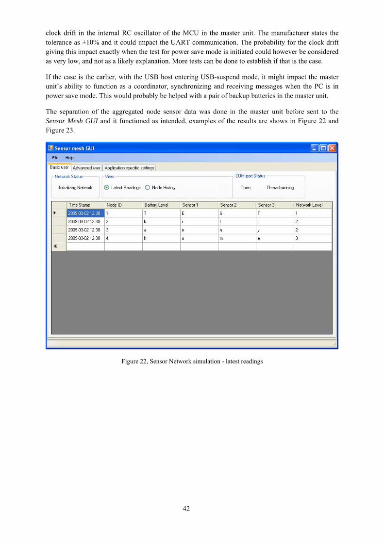
clock drift in the internal RC oscillator of the MCU in the master unit. The manufacturer states the tolerance as ±10% and it could impact the UART communication. The probability for the clock drift giving this impact exactly when the test for power save mode is initiated could however be considered as very low, and not as a likely explanation. More tests can be done to establish if that is the case.
If the case is the earlier, with the USB host entering USB-suspend mode, it might impact the master unit’s ability to function as a coordinator, synchronizing and receiving messages when the PC is in power save mode. This would probably be helped with a pair of backup batteries in the master unit.
The separation of the aggregated node sensor data was done in the master unit before sent to the Sensor Mesh GUI and it functioned as intended, examples of the results are shows in Figure 22 and Figure 23.
Figure 22, Sensor Network simulation - latest readings
42

Figure 23, Sensor network simulation - node history
7.2 Node Current Consumption
7.2.1 Results The theoretical current consumption has been calculated based on values from the MCU and Transceiver datasheets [109,113]. Components and additional functionalities in the MCU23 with lesser impact on the current consumption have not been considered in the calculations, as they will be turned on and off depending on the situation. The actual consumption was measured in test 12, see the test report in appendix E.
Table 8 shows the current consumption of a node during different operational conditions. The actual current consumption of the node is higher than the theoretical values. The greatest difference in current consumption, relative to the theoretical values, is seen when the transceiver is either transmitting or receiving. One possible reason for this is that the design of the filterbalun does not perfectly follow the reference design. The distance to the ground plane is shorter, and therefore it could degrade the impedance matching, which leads to a higher current consumption. The fact that no peripheral units current consumption has been taken into consideration in the theoretical values also give a difference. These current consumption figures should be a good platform for a low power WSN protocol. A simplified scenario is given in chapter 7.2.2 Simplified Lifetime Scenario, and a worst-case scenario is given in chapter 7.2.3 Worst-case Lifetime Scenario.
23 I.e. SPI and timer functionality etc.
43

Operational conditions. All measurements where done in room temperature (20-25 oC).
Measured current consumption
Measured power consumption
Theoretical current consumption (MCU + Radio)
MCU active 1Mhz, radio sleep @ 2.9V
0,6 mA 1,74 mW 0.55mA + 0.5 μA
MCU active 1Mhz, radio active, no TX/RX @ 2.9V
2,4 mA 6,96 mW 0.55 mA + 1.7 mA
MCU active 1Mhz, radio transmitting @ 3.0V, 2.6V, 1.9V and 0dB.
20.91mA, 19.45mA, 16.80mA
62,7 mW, 50,6 mW, 31,92 mW
0.55 mA + 16.8 mA, N/A, N/A
MCU active 1Mhz, radio receiving @ 3.0V, 2.6V, 1.9V, 38.4 kBaud.
21.35mA, 19.83mA, 17.07mA
64,1 mW, 51,6 mW, 32,4 mW
0.55 mA + 14.6 mA, N/A, N/A
MCU sleep, radio sleep @ 3.0V 9μA 27 μW 7,5μA + 0.5 μA
Table 8, Current consumption
7.2.2 Simplified Lifetime Scenario Assume a data rate of 38.4kBaud with GFSK modulation, a transmission overhead of 32 bit preamble followed by 2 x 16 bit sync words, 8 length bits, 8 address bits and an 16 bit CRC after the data. This is a possible setup with the CC1101 [113]. Most other configuration of the transceiver will have a higher baud rate and/or less overhead, giving less consumed power during transmission24. Depending on the amount of data sent, the TX/RX time can be calculated, along with the current consumption. In the simplest case, with only one node, sending 8 bits nodeID, 8 bits battery level, 24 bits sensor data and 8 bits network level, the total amount of bits in a transmission would be 144 bits. With 1% packet error rate the average would be 145,44 bits. GFSK modulation gives one symbol (baud) per bit, this means it will take 3,79 ms to transmit an average packet. If the time during start-up and shut down of the transceiver can be averaged to 1 ms (721+88+0,1 μs) [113] the total time of the transmission procedure would be 4,79 ms. Given a period time between transmissions of 1 hour, the average transmit current consumption can be calculated with equation 7. At 3V battery supply voltage; TTransmission = 0,00479 s, TTotal = 3600 s, ITransmitting = 20,9 mA. This gives an average of 2,78*10-5 mA due to transmission.
( ) sionToTransmisAverageDuengTransmittitotal
ontransmissi IIT
=×T
Due to any possible differences in frequencies and clock drift in the 32.768 kHz oscillator crystals [117], the master would also have to broadcast synchronization messages within certain intervals. The period of these synchronization messages would depend on the maximum deviation in crystal frequencies among the nodes, the clock drift, the length of the preamble of a transmission, the baud rate, and the amount of bits in a preamble the receiver must receive to accept it as a preamble, as well
[mA] [7]
24 Doubled baud rates will not double the current consumption [113].
44

as any differences in execution time in the separate nodes before enabling their transceiver after wakeup. As this is an extremely simple scenario, the synchronization period can be estimated to once every minute. With the present low frequency crystal having typically ±20 ppm tolerance, the maximum drift between the master and the node should be 60*40=240 µs during that time span. The master would only need to send one data byte, for the node to interpret it as a synchronization message. This would make the packet 104 bits long, and it would take in average 2,74 ms to receive it, if 1% packet error rate is considered. To be on the safe side, the transceiver can be put in active receiver mode a little bit earlier than necessary, say 1 ms. They can also drift the other direction, where the transmission comes later than expected. Add another 1 ms for this. In addition, the start up and initialization would take 1 ms, as when transmitting. Total time would be 5,74 ms. The average synchronization current consumption can now be calculated with equation 8. At 3V supply voltage; Tsync = 0,00574 s, nsync = 60 times/hour, Ttotal = 3600 s, IReceiving = 21,4 mA. This gives an average of 2,29*10-3 mA due to synchronization.
( ) ToSyncAverageDueceivingTotal
syncsync II
TT
n =×× Re
The average power consumption during the rest of the cycle, when sleeping, can be calculated with equation [9]. At 3V battery supply voltage; ISleep = 0,009 mA. This gives an average of 8,999*10-3 mA.
ToSleepAverageDueSleepTotal
syncsynconTransmissiTotal IIT
TnTT=×
×−−
These averages added together give the total average current consumption in the node, equation [10]. It would be 0,0113 mA.
geTotalAveraToSleepAverageDueToSyncAverageDuesionToTransmisAverageDue IIII =++
Depending on the characteristics of the battery, the lifetime of the node can be calculated. The easiest battery to consider might be the primary alkaline or lithium variants, with close to linear discharge curves down to approximately 0.8-0.9V and low self-discharge rates compared to other battery types. As it is still a simple scenario, the self-discharge25 of the battery is neglected to begin with, as well as the lower current consumption of the nodes when they are supplied a lower voltage. If the voltage decrease is linear, and self-discharge is neglected, equation 11 can be used to calculate the node lifetime. The batteries are connected in series. UICMin = 1.8V in the nodes developed in this solution, so the non-linearity in the discharge rate below 0.8-0.9V will not have any impact on the calculation. If the battery capacity is 2400 mAh and the initial supply voltage is 3V (2 alkaline AA batteries), the lifetime would be 84993 hours = 3541 days = 9,7 years.
[ ][ ] LifetimemAI
mAhcapacityBattery
UU
geTotalAveraNewBattery
ICMin =×⎟⎟⎠
⎞⎜⎜⎝
⎛−1
With a lifetime of a node of 9,7 years the self-discharge of the alkaline battery will most probably have a substantial impact on the lifetime of the node (many manufacturers state that their alkaline batteries have a shelf life of between 5-7 years). A conclusion of this is that in extreme cases where almost no traffic in the network is present, the lifetime of the nodes would be more dependant of choosing
[mA] [8]
[mA] [9]
[mA] [10]
[hours] [11]
25 The amount of charge in the battery is reduced over time, even if the battery can be considered not used.
45

batteries with low self-discharge than the actual current consumption of the hardware. Primary26 lithium batteries however are considered having lower self-discharge rates than alkaline batteries, and according to [118] they can have a shelf life27 of 10 years, making them a viable alternative if non-rechargeable batteries are preferred. Energizer sells primary lithium batteries with a shelf life of 15 years [119] where the shelf life is defined as having 90% capacity left.
In reality, with several nodes in a network, more data would be transmitted, consuming more power, and the choice of batteries would also impact the node lifetime greatly28. It is tempting to start to speculate in these kinds of matters, this would however force the writer of this report to intrude on the area of protocol design, which is not a part of this thesis.
It is easy to see however, that the power consumption during transmission of sensor data hardly has any impact on the calculated lifetime. The most important parts are the synchronization messages and the consumption during sleep. (That is - accurate oscillator crystals with small clock drift and components with low power consumption during sleep are very important for the lifetime). Adding more nodes and network levels to the network will of course increase the power consumption during the sensor data transmission procedure. Having a network with as few levels as possible, with a hierarchy with as few nodes as possible under each “higher” node in the hierarchy should keep the consumption as levelled as possible amongst the nodes. Having a master unit with long-range capabilities can keep the amount of levels low. Having individual nodes with long-range capabilities can however create scenarios where a few nodes are “hierarchical parents” to a great number of nodes, and therefore their power consumption will be higher.
Another aspect that can be considered is the battery recovery effect [6]. This effect prolongs battery life, appearing when the battery usage is “bursty”.
7.2.3 Worst-case lifetime scenario A worst case scenario would be where a node has 1% duty cycle of its transmissions and 1% duty cycle on incoming transmissions (if the incoming transmissions are more than 1% it would not be possible to retransmit all the data, and a backlog would occur. This is more related to the protocol part of a WSN and is therefore not considered). One example of a scenario where a node handles great amounts of data can be seen in Figure 24.
To account for clock drifts in nodes the receiver would have to be active listening longer than the time it is actually receiving data. The initialization of the node after exiting power save mode would also have to be considered. To be consistent, the estimations of these times, from 7.2.2 Simplified Lifetime Scenario, should be used. When transmitting the active duty cycle would be 4,79/3,79 = 1,26%. Likewise the active duty cycle when receiving would be 5,74/2,74 = 2,09%. Equations 12 and 11 give an estimation of the worst-case scenario lifetime. If the battery capacity is 2400 mAh and the initial supply voltage is 3V (two alkaline AA-batteries), the lifetime would be 1334 hours = 55 days. In this case it is made obvious that some kind of on-board recharging or energy scavenging functionality would be necessary to give the node a more reasonable lifetime.
geTotalAveraSleepceivingngTransmitti I
III=
−−×+×+×
100)09,226,1100(09,226,1 Re
[12]
26 Non-rechargable 27 When the battery only has 85-90% capacity left due to self-discharge, varying amongst manufacturers. 28Choosing batteries where not a part of this thesis, and therefore no further investigations in that matter has been done.
46
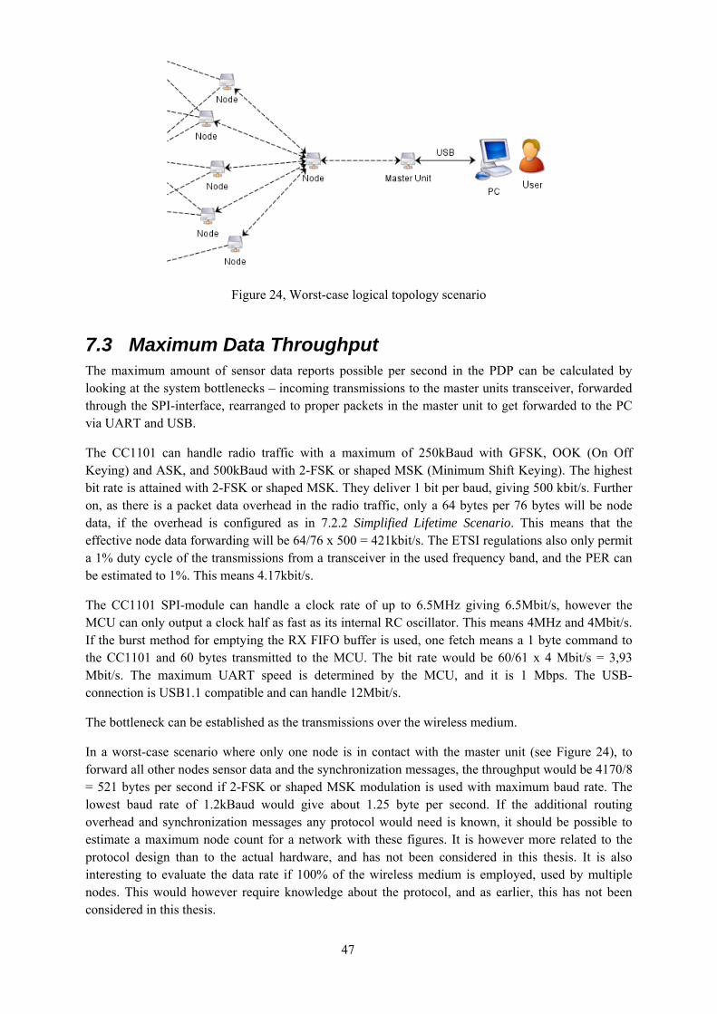
Figure 24, Worst-case logical topology scenario
7.3 Maximum Data Throughput The maximum amount of sensor data reports possible per second in the PDP can be calculated by looking at the system bottlenecks – incoming transmissions to the master units transceiver, forwarded through the SPI-interface, rearranged to proper packets in the master unit to get forwarded to the PC via UART and USB.
The CC1101 can handle radio traffic with a maximum of 250kBaud with GFSK, OOK (On Off Keying) and ASK, and 500kBaud with 2-FSK or shaped MSK (Minimum Shift Keying). The highest bit rate is attained with 2-FSK or shaped MSK. They deliver 1 bit per baud, giving 500 kbit/s. Further on, as there is a packet data overhead in the radio traffic, only a 64 bytes per 76 bytes will be node data, if the overhead is configured as in 7.2.2 Simplified Lifetime Scenario. This means that the effective node data forwarding will be 64/76 x 500 = 421kbit/s. The ETSI regulations also only permit a 1% duty cycle of the transmissions from a transceiver in the used frequency band, and the PER can be estimated to 1%. This means 4.17kbit/s.
The CC1101 SPI-module can handle a clock rate of up to 6.5MHz giving 6.5Mbit/s, however the MCU can only output a clock half as fast as its internal RC oscillator. This means 4MHz and 4Mbit/s. If the burst method for emptying the RX FIFO buffer is used, one fetch means a 1 byte command to the CC1101 and 60 bytes transmitted to the MCU. The bit rate would be 60/61 x 4 Mbit/s = 3,93 Mbit/s. The maximum UART speed is determined by the MCU, and it is 1 Mbps. The USB-connection is USB1.1 compatible and can handle 12Mbit/s.
The bottleneck can be established as the transmissions over the wireless medium.
In a worst-case scenario where only one node is in contact with the master unit (see Figure 24), to forward all other nodes sensor data and the synchronization messages, the throughput would be 4170/8 = 521 bytes per second if 2-FSK or shaped MSK modulation is used with maximum baud rate. The lowest baud rate of 1.2kBaud would give about 1.25 byte per second. If the additional routing overhead and synchronization messages any protocol would need is known, it should be possible to estimate a maximum node count for a network with these figures. It is however more related to the protocol design than to the actual hardware, and has not been considered in this thesis. It is also interesting to evaluate the data rate if 100% of the wireless medium is employed, used by multiple nodes. This would however require knowledge about the protocol, and as earlier, this has not been considered in this thesis.
47

7.4 Cost
7.4.1 Cost for Developing the PDP Hardware in this Thesis Table 9 and Table 10 shows the costs for designing and producing five prototype units; two master units and three nodes. The man hours required for the PDP hardware also accounts for the time needed to specify and chose circuits, as well as learning how to use the PCB design application. The numbers are meant to give an idea of how many resources a development of a WSN prototype requires. The prices include a pair of alkaline AA-batteries in the nodes.
Components PCB Total Cost/Master Unit (SEK, incl. VAT)
403 920 1323
Cost/Node (SEK, incl. VAT)
392 920 1312
Table 9, Material costs
Man hour Student hours
Syntronic Employee hours
Hardware 250 8,2 Software (PC) 100 0 Software (Protocol + misc. MCU functions)
N/A + 20
0
Table 10, Man-hours
The cost for the testing equipment and the software development tools has not been accounted for in this summary, as they would be expenses for the company even if no development had been done. Designing a casing for the nodes would also add some cost to the development. (The 3,5” diskette box used for one of the master units was free, but not very attractive!).
48

7.4.2 Mass Production Cost Provided that at least 10000 units29 are manufactured the component cost per unit would be 262 SEK for a master unit and 243 SEK for a regular node. Alkaline AA-batteries included. The cost of the components is based on Farnell prices the 5th of Mars 2009. A further iteration of the PCB, with smaller size (at least 1/4th of the size), cheaper plating (the prototypes has gold plating on the pads) and specialized design for the masters and the nodes would make the greatest difference in price. Employees at Syntronic’s Kista office estimate that the cost could go down to as low as 200 SEK per piece. If the SMA antenna with its connector is replaced by a PCB-antenna, the cost of the components would decrease further with about 80 SEK, with a degraded range of the communication as a consequence (The degradation has not been evaluated due to a lack of time).
The cost for mounting the components has not been considered in this example, as it would be done in a machine and no research has been done in that area. Man-hours for further development of the PDP is estimated to 150-200 hours for the hardware and 100-200 hours for the software, if skilled and experienced engineers are employed. Additional expenses may arise due to type approvals and testing. The competitiveness is discussed in chapter 8 - Conclusion, and the estimated mass production cost (10000+ units) is presented in Table 11.
Components PCB Total Cost/Master Unit (SEK, incl. VAT)
182 20030 382
Cost/Node (SEK, incl. VAT)
163 20030 363
Table 11, Mass production material costs
29 Nodes and master units added together 30 Estimation done by Syntronic Employees
49
8 CONCLUSION
8.1 Discussion
8.1.1 General Discussion The hardware developed in this thesis has been inspired by already existent motes, mainly the ones developed at the University of Berkeley, LA. They are equipped with an MCU and a transceiver, and have onboard USB-support. This thesis has further iterated the concept with USB-support only on the master unit, to lower the manufacturing cost and the power consumption, and it is also equipped with a MOSFET smart switch to control the power supply to sensors, so they do not consume power when the nodes are asleep. The functionality of the PC software was based on requirements from Syntronic.
The PDP hardware developed in this thesis has several advantages, as well as drawbacks, to already existent solutions. Seen from Syntronic’s point of view, it has a lower cost and it also have lower power consumption than most available motes, and no present known mote is better in both aspects. Another strength is the fast and competent support Syntronic will be able to give their customers since they have access to all the development documents and original schematics. They have the possibility to modify the PC and MCU software without having to contact any supplier. The platform should suit perfectly for customer-specific product solutions where the protocol and the PC software can be tailor made for its application. The actual frequency band used can also be considered an advantage. Compared to for instance the 2.4GHz band the 868 MHz band has a lower utilization. The 2.4GHz band is crowded with for instance ZigBee, Bluetooth and WLAN communication.
A further iteration of the PDP should without hesitation be able to compete on a global market, provided Syntronic has the resources to market it. Potential customers may already be interested in Malaysia31. The question is if the money and time spent on a further development is worth it. It might be cheaper in the end to just buy any semi-finished solution, especially considering the dependency of the completion of the protocol.
The biggest drawback is probably the lack of compatibility to the ZigBee/IEEE 802.4.15 - protocol stack. ZigBee/IEEE 802.4.15 can operate on the 868MHz band, but the standard utilizes BPSK-modulation in that channel [120], which the CC1101-transceiver does not support32. The MCUs used also lacks the RAM required for running the ZigBee software. In the event of that no protocol is finished in the parallel thesis by Fredrik Smitt, and no further efforts are to be made from Syntronic in the area, the future iteration of the prototype can be modified with for instance an Atmega1281V-8AU MCU and an 802.4.15-compliant transceiver. The Atmega1281-8AU has the same footprint and pinout as the Atmega645V-8AU used in this thesis, but has more RAM and a higher cost. 802.4.15-compliant transceivers are also more expensive relative to the CC1101 as of the 9th of Mars 2009. Examples of Farnell’s ZigBee-compliant devices can be found here [121]. Syntronic would in this case most certainly make greater profit from integrating WeBee motes in their solutions instead of developing new hardware.
Since the beginning of this thesis, Z-wave has also released an “outdoor-variant” of their solution. As Syntronic already has experience from Z-wave they might be interested in looking at it, although, they still only support 232 nodes and their protocol is inefficient from power consumption point-of-view. 31 Email correspondence between David Näslund, Magnus Söderlind, Syntronic Kista and Lee Siak Hong, General manager Syntronic Malaysia 32 Further on, IEEE 802.4.15 standards maximum bit rate in the 868 MHz band is limited to 20kbps. The CC1101 can handle 250kbps with GFSK or 500kbps with 2-FSK.
50

The results of the simplified lifetime scenario shows that in very small networks where very little data is sent very seldom (for instance in household use, where a light-switch unit turn on and of the light) it is more important with low self-discharge of the batteries than optimizing low power consumption. Further on the results of the worst-case scenario shows that it is necessary to implement some kind of energy scavenging (for instance solar cells) to prolong the node lifetime in nodes handling larger amounts of data. Both results point in the direction where power consumption might not be the most critical characteristic of a node, as long as it is low enough to be supplied by any kind of energy scavenging device.
8.1.2 Follow-up on Requirements Most if not all of the functional requirements setup in the initial phase has been met. It is unclear if any regulations regarding spurious emissions are violated, due to the lack of necessary test equipment at Syntronic’s office. The requirement of a clear and intuitive graphical user interface on the PC is fulfilled from Syntronic’s point of view; it is however a matter of personal opinion and maybe the end-customer finds it un-intuitive. The future might tell.
If the additional aims to make a prototype having an “as low power consumption and cost as determined possible” are fulfilled is open for discussion. As it is a master thesis project, the cost for employing an engineer to do the same work has been cut, and that is a huge saving for the company. However, the production cost33 of the PDP hardware can be considered being high from Syntronics point of view compared to at least two already present solutions (Mica2 and WeBee). With greater quantities and smaller, purpose-specific PCBs for nodes and master units the cost of the PCBs can be lowered. Based on the amount of free space on the PCB the size of the PCBs can be reduced to at least 25% if smaller components are used and a more skilled PCB designer do the routing. The PCBs can also be manufactured in China for lower manufacturing costs, as long as the manufactured volumes are large enough to cover for the shipping costs34. The cost per node/master unit will probably never be lower than that of the WeBee, but the cost per unit can be made far lower than buying any of the other present solutions, all costing more than 1000 SEK.
The Mulle probably35 has lower power consumption than this prototype during sleep36. Compared to the other motes in Table 2 except the Mulle, the prototype developed in this thesis cut 50-75% of the power consumption during sleep. During RX/TX the consumption is 20-60% lower.
As one mote solution (WeBee) has a lower price than will be possible to achieve with this solution, and another solution (Mulle) a probable lower power consumption, this particular prototype in this thesis can be considered a compromise between the two, making an “as low as possible” cost and power consumption solution, based on the requirements.
The aim to make error free PC software can be considered non-fulfilled. It has several minor bugs and limitations that can be corrected, for instance the node list when choosing to display node history, it appears twice. The node history radio button also seems bugged and it might be related to the previous bug.
It was realized fairly early in the thesis that a node map was going to be one of the later things to implement, and the aim was left unengaged in the end.
33 Components and PCB manufacturing 34 Email correspondence with Lily Chen, Syntronic China Office 35 The information given by the suppliers are limited and unclear. 36 It is however expensive and the Bluetooth technology gives limitations on the usability of a network based on the platform, so it is still not a good option.
51

8.2 Future Work Future work can be divided into two areas; Future work regarding the work done in this thesis, and future work and recommendations regarding any further iterations of the prototype. Future work related to the PDP produced in this thesis:
• More advanced testing of radio transmission range and validating that the spurious emissions from the transceiver circuit do not exceed ETSIs regulations. (Syntronic Kista does not have the testing equipment necessary for these kinds of tests)
• Fine-tuning the oscillator crystals by testing their frequencies at different load capacitances. • Do long-term tests of the crystals to determine their actual clock drift. • There is a bug when choosing nodes in the node list – the list appears twice. • Test the nodes with real, external sensors, not just the built-in transceiver thermometer.
Future work and recommendations if iterating the concept, provided that an evaluation has shown that there is any profitability in it:
• Equip the master unit with a mechanism for rechargeable backup batteries to enable its functionality when the computer is turned of. This could also eliminate any potential problems when the PC enters power save mode.
• With a flash memory stick on the master unit, sensor data could be logged while Sensor Mesh GUI is turned off. With the previously mentioned backup batteries, data could be logged even when the PC is turned off.
• Upgrade the MCU of the master unit so it can calculate the routes for larger networks than is possible today.
• Regarding the MCU of the nodes; it should be possible to find MCUs with fewer pinouts, and thereby smaller size. Also do tests to check if any of the pull-ups can be removed or given a higher resistance. Depending on volumes, maybe ASICs can be considered.
• The manufacturing cost of the hardware can be lowered if the PCB design is optimized. Designing a PCB-antenna instead of a ¼ whip SMA antenna should lower the cost significantly, however, this would probably lower the range of the wireless communication. Texas instruments provide reference designs of various PCB-antennas.
• By making sure the impedance matching of the antenna is guaranteed to be correct in further iterations of the hardware, it might be possible to lower the power consumption when receiving and transmitting.
• Enable choosing COM-port used for communication in Sensor Mesh GUI. • As of now, only the battery level ADC route employs voltage division. To eliminate the need for
voltage division in the sensor units, they could be in the PCB design as well. • Re-write the PC application to not only log and display incoming node data, but to also show
diagrams on the data history of different nodes. In addition to this, the “node map”-space reserved for the debugging in the advanced tab could be replaced by a real node map, showing the latest readings or the average readings from any time span.
• Introduce some sort of energy scavenging in the nodes, maybe solar cells together with rechargeable the batteries.
• Make specialized PCBs for the master units and the nodes. This will cut the manufacturing costs for both of them, during mass production.
• Design casings and sensor circuitry. Make sure the casing can shield the hardware from the environment.
• Evaluate energy scavenging methods.
52
9 REFERENCES
53
[1] Prel. title: Research and Development of a Wireless Sensor Network Protocol, F. Smitt, (2009)
[2] Wireless Sensor Networks for Smart Crops, http://onworld.com/smartcrops/index.html (September, 2008)
[3] Water Crisis – Wikipedia the free encyclopedia, http://en.wikipedia.org/wiki/Water_crisis (September, 2008)
[4] Sensornetworks, T. Haenselmann (2006) Available at http://www.informatik.uni-mannheim.de/~haensel/sn_book/sensor_networks.pdf (October 2008)
[5] HPEQ- A Hierarchical Periodic Event Driven and Query Based Wireless Sensor Network Protocol, A. Boukerche, R.W.N. Pazzi, R.B. Aranjo, university of Ottawa, The IEEE Conference on Local Computer Networks (2005)
[6] Wireless Sensor Networks, ISBN 0-8493-1823-8, E.H. Callaway Jr., Published by Auerbach publications – A CRC Press Company (2004)
[7] ALOHA Packet Broadcasting: A Retrospect, R. Binder, N. Abramson, F. Kuo, A. Okinaka, D. Wax, available at http://research.microsoft.com/~gbell/Computer_Structures_Principles_and_Examples/csp0432.htm (December, 2008)
[8] Wireless integrated network sensors, ISSN 0001-0782, G.J. Pottie, W.J. Kaiser, Published by ACM (2000)
[9] Performance Analysis and Optimisation of a 2.4GHz,Multi-Hop, Wireless Self-Configurable Network, R. Stutz, U.C Berkeley, Projet de diplôme en électronique (2003)
[10] μAMPS Home, http://www-mtl.mit.edu/researchgroups/icsystems/uamps/ (November 21, 2008)
[11] Handbook of Sensor Networks: Compact Wireless and Wired Sensing Systems, page 3 chapter 1, ISBN 0-8493-1968-4 M. Ilyas, I. Mahgoub, Published by CRC Press LLC (2005)
[12] Wireless Sensors to Modernize Parking, http://www.wi-fiplanet.com/columns/article.php/3696701 (September, 2008)
[13] Atmel Products – Microcontrollers – MCU wireless solutions, http://www.atmel.com/products/zigbee/default.asp (November 21, 2008)
[14] Low Power Wireless RF Solutions, ZigBee, RFID, RF/IF – TI.com, http://focus.ti.com/analog/docs/rfifcomponentshome.tsp?familyId=367&contentType=4&DCMP=TIHomeTracking&HQS=Other+OT+home_p_rf_if (November 21, 2008)
[15] A Survey on Sensor Networks, I.F. Akyildiz, W. Su, Y. Sankarasubramaniam, E. Cayirci, Georgia Institute of Technology, In IEEE Communications Magazine (2002)
[16] Wireless sensor network survey, J. Yick, B. Mukherjee, D. Ghosal, In Computer Networks Volume 52, Issue 12, 22 August 2008, pages 2292-2330. Published by Elsevier B.V. (2008)
[17] Wireless mesh networks: a survey, I.F. Akyildiz, X. Wang, W. Wang, In Computer Networks Volume 47, Issue 4, 15 March 2005, pages 445-487. Published by Elsevier Science B.V. (2004)
[18] A Survey of Transport Protocols for Wireless Sensor Networks, C. Wang and K. Sohraby, University of Arkansas and B. Li, The Hong Kong University of Science and Technology and M. Daneshmand, AT&T Labs Research and Y. Hu, South China Agricultural University, In IEEE Network Volume 20, Issue 3, May-June 2006, pages 34–40 (2006)
[19] CODA: Congestion Detection and Avoidance in Sensor Networks, C-Y. Wan, S.B. Eisenman, and A.T. Campbell, In proceedings of the 1st international conference on Embedded networked sensor systems (2003)
[20] Mitigating Congestion in Wireless Sensor Networks, B. Hull, K. Jamieson, and H. Balakrishnan, In proceedings of the 2nd international conference on Embedded networked sensor systems (2004)
[21] Congestion Control and Fairness for Many-to-One Routing in Sensor Networks, C.T. Ee and R. Bajcsy In proceedings of the 2nd international conference on Embedded networked sensor systems (2004)
[22] A Transmission Control Scheme for Media Access in Sensor Networks, A. Woo, D.E. Culler, In proceedings of the 7th annual international conference on Mobile computing and networking (2004)

54
[23] PSFQ: A Reliable Transport Protocol for Wireless Sensor Networks, C-Y. Wan, A.T. Campbell, L.
Krishnamurthy, In proceedings of the 1st ACM international workshop on Wireless sensor networks and applications (2002)
[24] ESRT: Event-to- Sink Reliable Transport in Wireless Sensor Networks, Y. Sankarasubramaniam, Ö.B. Akan, I.F. Akyildiz, In proceedings of the 4th ACM international symposium on Mobile ad hoc networking & computing (2003)
[25] Reliable Bursty Convergecast in Wireless Sensor Networks, H. Zhang, A. Arora. Y-R. Choi, M.G. Gouda, In proceedings of the 6th ACM international symposium on Mobile ad hoc networking and computing (2005)
[26] A Scalable Approach for Reliable Downstream Data Delivery in Wireless Sensor Networks, S-J. Park, R. Vedantham, R. Sivakumar, I.F. Akyildiz, In proceedings of the 5th ACM international symposium on Mobile ad hoc networking and computing (2004)
[27] Delay aware reliable transport in wireless sensor networks, V.C. Gungor, Ö.B. Akan, In International Journal of Communication Systems Volume 20, Issue 10, October 2007, pages 1155–1177. (2007)
[28] PORT: a price-oriented reliable transport protocol for wireless sensor network, Y. Zhou, M.R Lyu, J. Liu, H. Wang, In proceedings of the 16th IEEE International Symposium on Software Reliability Engineering (2005)
[29] Delay sensitive transport in wireless sensor networks, V.C. Gungor, Ö.B. Akan, In 2006 International Symposium on Computer Networks, pages 116-122. (2006)
[30] STCP: A Generic Transport Layer Protocol for Wireless Sensor Networks, Y. G. Iyer, S. Gandham, S. Venkatesan, In proceedings of the 14th International Conference on Computer Communications and Networks, pages 449-454. (2005)
[31] Routing Techniques in Wireless Sensor Networks: a Survey, J.N. Al-Karaki, The Hashemite University and A.E. Kamal, Iowa State University, In IEEE Wireless Communications, Volume 11, Issue 6, Dec. 2004, pages 6-28. (2004)
[32] Energy Aware Routing for Low Energy Ad Hoc Sensor Networks, R.C. Shah, J.M. Rabaey, University of California, Berkeley, In IEEE Wireless Communications and Networking Conference, Volume 1, pages 350-355. (2002)
[33] Energy-efficient communication protocols for wireless microsensor networks, W.R. Heinzelman, A. Chandrakasan, H. Balakrishnan, In proceedings of the 33rd Hawaii International Conference on System Sciences, Volume 8. (2000)
[34] Ad-hoc On-demand Distant Vector Routing, I.D. Chakeres, E.M. Belding-Royer, In Proceedings of the second IEEE Workshop on Mobile Computing Systems and Applications, pages 90-100. (1999)
[35] An Adaptive Energy Efficient MAC Protocol for Wireless Sensor Networks, T. van Dam, K. Langendoen, In proceedings of the 1st international conference on Embedded networked sensor systems, pages 171-180 (2003)
[36] An energy-efficient MAC protocol for wireless sensor networks, W. Ye, J. Heidemann, D. Estrin, In proceedings of INFOCOM 2002. The Twenty-First Annual Joint Conference of the IEEE Computer and Communications Societies, Volume 3, pages 1567-1576. (2002)
[37] Versatile low power media access for wireless sensor networks, J. Polastre, J. Hill, D. Culler, In proceedings of the 2nd international conference on Embedded networked sensor systems, pages 95-107 (2004)
[38] Low power MAC protocols for infrastructure wireless sensor networks, A. El-Hoiyi, J.D. Decotignie, J. Hernandez, In proceedings of the Fifth European Wireless Conference (2004)
[39] Ultra-Low Duty Cycle MAC with Scheduled Channel Polling, W. Ye, F. Silva, J. Heidemann, In proceedings of the 4th international conference on Embedded networked sensor systems, pages 321-334 (2006)
[40] SEA-MAC: A Simple Energy Aware MAC Protocol for Wireless Sensor Networks for Environmental Monitoring, M. Erazo, Y. Qian, ISWPC’07. 2nd International Symposium on Wireless Pervasive Computing (2007)

55
[41] Z-MAC: a Hybrid MAC for Wireless Sensor Networks, A. Warrier, J. Min, I. Rhee, In proceedings of the
3rd international conference on Embedded networked sensor systems, pages 90-101 (2005)
[42] Analysis and Design of a MAC Protocol for Wireless Sensor Network with Periodic Monitoring Applications. M.A. Erazo, Y. Qian, K. Lu, D. Rodriguez, IEEE Military Communications Conference 2007, pages 1-7 (2007)
[43] Medium access control with coordinated adaptive sleeping for wireless sensor networks, W. Ye, J. Heidemann, D. Estrin, IEEE/ACM Transactions on Networking, Volume 12 , Issue 3 (June 2004), pages 493-506 (2004)
[44] An adaptive energy-efficient and low-latency MAC for data gathering in sensor networks, G. Lu, B. Krishnamachari, C. Raghavendra, In proceedings of the 18th International Parallel and Distributed Processing Symposium (2004)
[45] Energyefficient, collision-free medium access control for wireless sensor networks, V. Rajendran, K. Obraczka, J.J. Garcia-Luna-Aceves, In proceedings of the 1st international conference on Embedded networked sensor systems, pages 181-192 (2006)
[46] A bit-map-assisted energy-efficient MAC scheme for wireless sensor networks, J. Li and G. Lazarou, In proceedings of the 3rd international symposium on Information processing in sensor networks, pages 55-60 (2004)
[47] A lightweight medium access protocol (LMAC) for wireless sensor networks, L. van Hoesel, P. Havinga, In 1st International Workshop on Networked Sensing Systems, pages 205-208 (2004)
[48] PAMAS: Power aware multi-access protocol with signaling for ad hoc networks, S. Singh, C.S. Raghavendra, ACM SIGCOMM Computer Communication Review, Volume 28 , Issue 3 (July 1998), pages: 5-26 (1998)
[49] STEM: Topology Management for Energy Efficient Sensor Networks, C. Schurgers, V. Tsiatsis, and M. B. Srivastava, In the IEEE Aerospace Conference Proceedings, Volume 3, pages 1099-1108 (2002)
[50] PMAC: An Adaptive Energy-Efficient MAC Protocol for Wireless Sensor Networks, T. Zheng, S. Radhakrishnan, V. Sarangan, In proceedings of the 19th IEEE International Parallel and Distributed Processing Symposium (IPDPS'05), Workshop 12, Volume 13 (2005)
[51] ET-MAC: An Energy-Efficient and High Throughput MAC Protocol for Wireless Sensor Networks, H.S. Aghdasi, M. Abbaspour, From 6th annual Communication Networks and Services Research Conference, pages 526-532 (2008)
[52] The energy-per-useful-bit metric for evaluating and optimizing sensor network physical layers, J. Ammer, J. Rabaey, From 3rd Annual IEEE Communications Society on Sensor and Ad Hoc Communications and Networks, Volume 2, pages 695-700 (2006)
[53] TinyOS Community Forum || An open-source OS for the networked, http://www.tinyos.net/ (October 8, 2008)
[54] The Contiki Operating System – Home, http://www.sics.se/contiki/ (October 8, 2008)
[55] The Contiki Operating System – About Contiki, http://www.sics.se/contiki/about-contiki.html (October 8, 2008)
[56] The Sensor Network Museum : Main - Home Page browse, http://www.btnode.ethz.ch/Projects/SensorNetworkMuseum (October 6, 2008)
[57] Mini hardware survey, http://www.cse.unsw.edu.au/~sensar/hardware/hardware_survey.html (October 6, 2008)
[58] Sensor Node, Wikipedia, the free encyclopedia, http://en.wikipedia.org/wiki/Sensor_node (October 7, 2008)
[59] University of California, Berkeley, http://berkeley.edu/ (October 6, 2008)
[60] Crossbow Technology, http://www.xbow.com (October 6, 2008)
[61] Sentilla | Energy Management Solutions, http://www.sentilla.com (October 7, 2008)
[62] Webee flyer, http://www.btnode.ethz.ch/pub/uploads/Projects/webee_flyer.pdf (October 6, 2008)
[63] Crossbow Technology:TelosB, http://www.xbow.com/Products/productdetails.aspx?sid=252( September 26, 2008)

56
[64] ZigBee/IEEE 802.15.4 Summary, Sinem Coleri Ergen (2004)
[65] Low Power Consumption Features of the IEEE 802.15.4/ZigBee LR-WPAN Standard, Ed Callaway, Technical Report, (2003)
[66] Part 15.4: Wireless Medium Access Control (MAC) and Physical Layer (PHY) Specifications for Low-Rate Wireless Personal Area Networks (WPANs). (IEEE Std 802.15.4a™-2007).
[67] Tmote Sky datasheet, http://www.btnode.ethz.ch/pub/uploads/Projects/tmote_sky_datasheet.pdf (October 7, 2008)
[68] Mica2 datasheet, http://www.xbow.com/Products/Product_pdf_files/Wireless_pdf/MICA2_Datasheet.pdf (October 7, 2008)
[69] The Sensor Network Museum : Projects - Mica 2 browse, http://www.btnode.ethz.ch/Projects/Mica2 (October 7, 2008)
[70] The Mulle – A Bluetooth-equipped sensor node, http://www.csee.ltu.se/~jench/mulle.html (October 7, 2008)
[71] SunSPOTWorld - Project Sun SPOT Products, http://sunspotworld.com/products/ (October 7, 2008)
[72] Webee Flyer, http://www.btnode.ethz.ch/pub/uploads/Projects/webee_flyer.pdf (October 7, 2008)
[73] Z-Wave Developer's Kit ver. 4.23
[74] Zensys – Zensys, http://www.zen-sys.com/modules/Zensys/ (October 6, 2008)
[75] Crossbow Technology : Eko : eKo – Technology, http://www.xbow.com/Eko/eko_technology1.aspx (September 26, 2008)
[76] Crossbow Technology : Eko : eKo – Shopping, http://www.xbow.com/Eko/eko_shopping.aspx (September 26, 2008)
[77] Crossbow_eKo_Wireless_Crop_Monitoring, http://www.xbow.com/General_Info/Info_pdf_files/Crossbow_eKo_Wireless_Crop_Monitoring.pdf (September 26, 2008)
[78] Wireless Sensor Networks, http://www.sensornets.csiro.au/ (October 6, 2008)
[79] Sensicast: SensiNet Overview, http://www.sensicast.com/products.php (September 25, 2008)
[80] A Mote in the Eye of the Wireless Universe?, http://www.wi-fiplanet.com/columns/article.php/3698386 (October 7, 2008)
[81] Honeywell New Release, http://content.honeywell.com/sensing/pressreleases/2006/wireless.pdf (October 7, 2008)
[82] WirelessHART Specification Recognized by International Standards Body, http://www.hartcomm2.org/mainpage_articles/wirelessHART_approved_by_IEC.html (October 7, 2008)
[83] Rosemount Analytical – 6081 Smart Wireless Transmitter, http://www.emersonprocess.com/raihome/liquid/products/model_6081.asp (October 7, 2008)
[84] David Näslund, Oral communication, Syntronic AB, Kista Office (Autumn, 2008)
[85] IPC 2221A Generic Standard on Printed Board Design (2003)
[86] IPC 2222 Sectional Design Standard for Rigid Organic Printed Boards (1998)
[87] C-J. Ohlson, Oral communication, Syntronic AB, Kista Office (October, 2008)
[88] A. Ek, Oral communication, Syntronic AB, Gävle Office, telephone contact (October, 2008)
[89] Decoupling, http://www.hottconsultants.com/techtips/decoupling.html (December 19, 2008)
[90] Henry Ott Consultants homepage, www.hottconsultants.com (October, 2008)
[91] Texas Instruments Design note DN017 - CC11xx 868/915 MHz RF Matching, A. Andersen, C. Seem, F. Storvik
[92] SFS Lag (2003:389) om elektronisk kommunikation, http://www.riksdagen.se/webbnav/index.aspx?nid=3911&dok_id=SFS2003:389&rm=2003&bet=2003:389 (February 9, 2009)
[93] PTSFS 2007:4: 6 kap §12

57
[94] PTSFS 2007:4: 6 kap §1
[95] Draft ETSI EN 300 220-1 V2.2.1 (2008-04)
[96] PTSFS 2007:4: 5 kap §1
[97] CADInt.se, http://www.cadint.se/products.asp (January 21, 2009)
[98] Date Sheets, http://www.101science.com/rfdesign.htm (January 21, 2009)
[99] Atmel Products – Tools & Software, http://www.atmel.com/dyn/products/tools_card.asp?tool_id=2725 (November, 2008)
[100] Sourceforge.net: WinAVR, http://sourceforge.net/projects/winavr (November, 2008)
[101] KernelPro.com –Home – virtual serial port driver – USB over network, http://www.kernelpro.com/ (November, 2008)
[102] Microsoft Visual Studio on MSDN, http://msdn.microsoft.com/sv-se/vstudio/default(en-us).aspx (September, 2008)
[103] FTDI Utilities, http://www.ftdichip.com/Resources/Utilities.htm#Mprog (February 12, 2009)
[104] NI LabVIEW - The Software That Powers Virtual Instrumentation - Products and Services - National Instruments, http://www.ni.com/labview/ (February 12, 2009)
[105] Realterm 1.13 Freeware Download... http://www.sourcecodeonline.com/details/realterm.html (February 12, 2009)
[106] Individually checked at the webpage The Sensor Network Museum, http://www.btnode.ethz.ch/Projects/SensorNetworkMuseum (October 8, 2008)
[107] ATmega64L datasheet, http://www.atmel.com/dyn/resources/prod_documents/2490S.pdf (October 8, 2008)
[108] ATmega128L datasheet, http://www.atmel.com/dyn/resources/prod_documents/2467S.pdf (October 8, 2008)
[109] ATmega645V datasheet, http://www.atmel.com/dyn/resources/prod_documents/doc2570.pdf (October 8, 2008)
[110] ATmega1281 datasheet, http://www.atmel.com/dyn/resources/prod_documents/doc2549.PDF (October 8, 2008)
[111] MSP430f156 datasheet, http://focus.ti.com/lit/ds/symlink/msp430f156.pdf (October 8, 2008)
[112] FT232R datasheet, http://www.ftdichip.com/Documents/DataSheets/DS_FT232R.pdf (October 4, 2008)
[113] CC1101 datasheet, http://focus.ti.com/lit/ds/symlink/cc1101.pdf (September, 2008)
[114] Control.Invoke Method (Delegate, Object[]) (System.Windows.Forms), http://msdn.microsoft.com/en-us/library/a1hetckb.aspx (Mars 2009)
[115] Design Note DN018, Range Measurements in an Open Field Environment, TI, T-I. Kvaksrud (2008)
[116] A. Jacobson, Oral communication, Syntronic AB, Kista Office (Mars 2, 2009)
[117] LF A103S – RAKON datasheet, http://www.farnell.com/datasheets/64638.pdf (October, 2008)
[118] Battery Performance Characteristics, http://www.mpoweruk.com/performance.htm (April, 2009)
[119] Energizer L91 Datasheet, http:// data.energizer.com/PDFs/l91.pdf (April, 2009)
[120] Modulation and Code Mapping Scheme for High Rate Transmission in 868MHz, Manjeet Singh, Zhongding Lei, Francois Chin and Y.S. Kwok, Conference Record of the Thirty-Ninth Asilomar Conference on Signals, Systems and Computers, pages 601-605 (2005)
[121] RF / IF Transmitters & Receivers | Farnell Sverige, http://se.farnell.com/jsp/search/browse.jsp?N=500014+1002571&Ntk=gensearch_001&Ntt=zigbee&Ntx= (Mars 9, 2009)

58
APPENDIX A
Acronyms and terminology
Abbreviations ACK Acknowledged ADC Analogue to Digital Converter AFA Adaptive Frequency Agility ASIC Application Specific Integrated Circuit ASK Amplitude Shift Keying – a modulation technique ASCII American Standard Code for Information Interchange C/C++/C# Programming languages COTS Commercial off-the-shelf CSMA Carrier Sense Multiple Access CSS Coordinated Sleep Schedules CRC Cyclic Redundancy Check CTS Clear To Send EEPROM Electronically Erasable Programmable Read Only Memory EIRP Equivalent Isotropically Radiated Power EMI ElectroMagnetic Interference ERP Effective Radiated Power ESD ElectroStatic Discharge ETSI European Telecommunications Standards Institute FPGA Field Programmable Gate Array FR4 Flame Retardant 4, a dielectric material used in PCBs FSK Frequency Shift Keying – a modulation technique FTDI Future Technology Devices International GFSK Gaussian Frequency Shift Keying – a modulation technique GND Ground GUI Graphical User Interface IC Integrated Circuit I2C Inter-Integrated Circuit – a kind of communication bus between ICs IDE Integrated Development/Design Environment IEEE Institute of Electrical and Electronics Engineers IPC Institute for Printed Circuits ISM Industrial Scientific and Medical – specific radio frequency bands ITU International Telecommunication Union JTAG Joint Test Action Group LBT Listen Before Transmit LPL Low Power Listening MAC Media Access Control MHz Megahertz, Unit for frequency. Million oscillations per second MSK Minimum Shift Keying – a modulation technique OOK On-Off Keying – a modulation technique OS Operating System PCB Printed Circuit Board QoS Quality of Service

59
PDP Prototype/Development Platform PER Packet Error Rate PSK Phase Shift Keying PTS Post- och Telestyrelsen PTSFS Post- och Telestyrelsens Författningssamling RAM Random Access Memory RF Radio Frequency RISC Reduced Instruction Set Computing RoHS Restriction of Hazardous Substances – a set of regulations ROM Read Only Memory RSSI Received Signal Strength Indication RTS Request To Send RX Receive SFS Sveriges Författningssamling SMA/SMB/SMC SubMiniature version A/B/C – antenna connectors SPI Serial Peripherals Interface – a kind of communication bus between ICs SRAM Static Random Access Memory TCP/IP Transmission Control Protocol / Internet Protocol TDMA Time Division Multiple Access – a scheduling method TX Transmission UART Universal Asynchronous Receiver/Transmitter – a kind of communication bus
between ICs USB Universal Serial Bus UWB Ultra Wide Band VCC/VDD Positive supply voltage WINS Wireless Integrated Network Sensors WSN Wireless Sensor Network Phrases and their meanings in this thesis COM port A serial port. Crosstalk When two conductors influence each other. Flooding When every node in the network broadcasts a message to all nodes in range,
after receiving it. The network gets “flooded” by the message. Master unit The ultimate control unit in a wireless sensor network. Usually it has some
kind of interface to another media. Mote The physical hardware units used when implementing nodes and routers in a
wireless sensor network. Network level How many wireless communication “hops” a node is from its master. Node A usually battery driven unit, communicating wirelessly with other nodes, a
routing unit or master unit. Parasitic inductance “Unwanted” inductance in a component (capacitance or resistor) or in a
conductor or a via hole. Permittivity How a dielectric material and an electric field affects each other Pin A metal surface or leg on an IC, acting as an interface to it. Different pins
have different functions, depending on IC. Port A collection of pins acting as a grouped interface for for instance
communication uses. PN9 sequence 9-bit Pseudo-random number.

60
Return currents The current flowing from an IC’s GND-pins back to the origin of the supplied
current. Router unit A node-like unit but with the extra task to control the communication in node-
node or node-master communication. Also called “cluster head”. Serial port A nine pin communication port on a PC. The standard is getting old and is
replaced by USB-ports on modern computers, which can look like serial ports on the PC with the right software.
Spurious emission A transmitted radio frequency not in the frequency band of in which the actual radio communication is taking place.
Whitening When a transmitter balances the amount of ones and zeroes transmitted, to keep the average transmitted power low on a certain frequency when using FSK modulation.

61
APPENDIX B
Schematics
The schematics of the hybrid master-node design. All different pages in the schematics are connected together, via ports.

62
Pin headers schematics page.
MCU related schematics page, part 1

63
MCU related schematics page part 2

64
Transceiver related schematics page, part 1
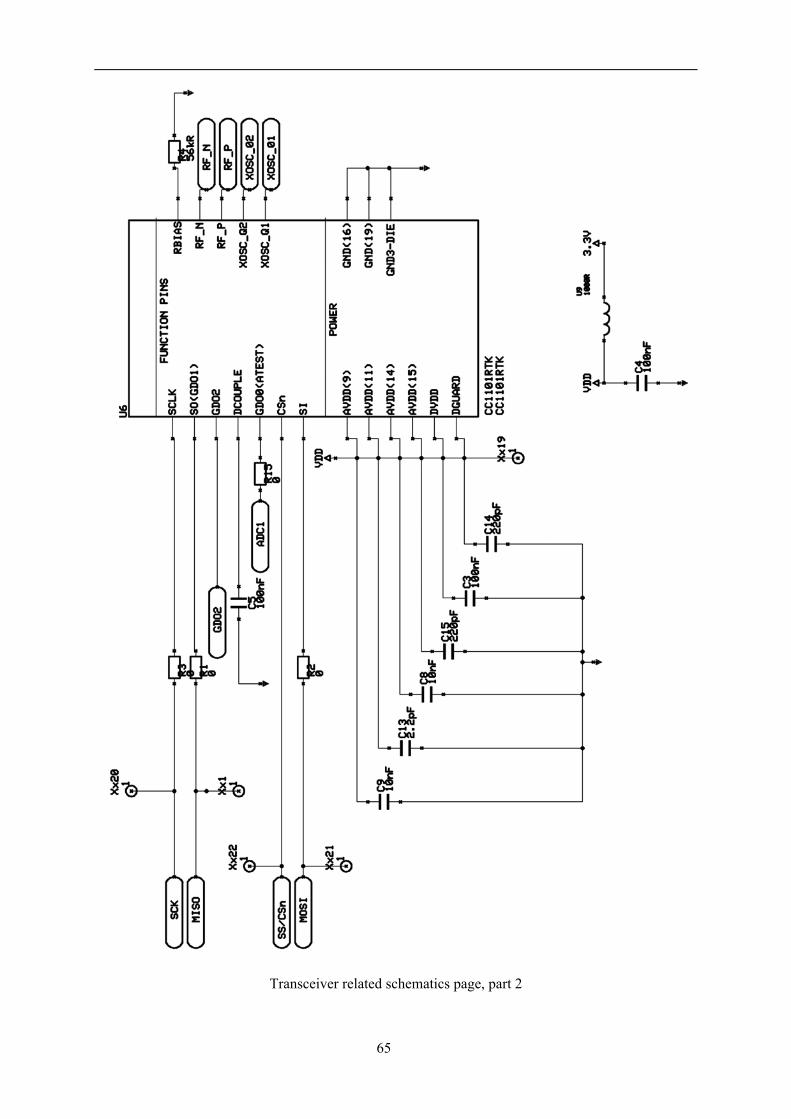
65
Transceiver related schematics page, part 2

66
FT232R and USB power supply related schematics page

67
APPENDIX C
PCB Layout
PCB copper layout of the different layers. Copper is visualized by black color. Drilled through holes are grey.
The top layer, primary routing layer.
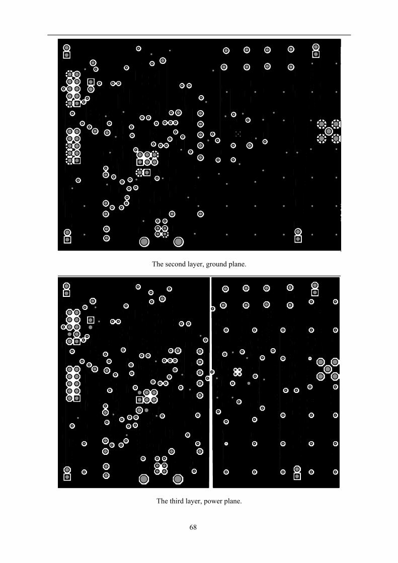
68
The second layer, ground plane.
The third layer, power plane.

69
The fourth layer, secondary routing layer.
PCB silkscreen.
70
APPENDIX D
Used Software
CADInt PCB CADInt PCB [97] is an application used when designing printed circuit boards. CADInt PCB provide tools to create schematics and layout for printed circuit boards with a maximum of 32 layers, depending on license agreements. It also provides tools to create footprints and 3D-shapes of components, to ease the development of circuit boards with restrictions in size and shape.
RFsim99 RFsim99 [98] is a freeware application used when calculating and simulating electrical properties of circuits, primarily RF designs.
AVR Studio AVR Studio [99] is freeware provided by Atmel, for writing code and programming their microcontrollers. It provides tools for software simulation as well as JTAG-debugging and In-System Programming. Version 4.13 build 557 was used in this thesis, since the newest version did not function properly with the JTAG debugger tool.
WinAVR WinAVR [100] is a set of free development tools for Atmel AVR RISC-microprocessors. It contains a compiler for C/C++, used by AVR Studio.
Advanced virtual COM port Advanced virtual COM port [101] is a utility providing the user possibilities to simulate COM ports on his or hers computer. It can also share COM ports over a LAN or the Internet. In this thesis, Advanced virtual COM port is used to create two virtual COM ports, connected to each other. This makes it possible for two applications to communicate with each other via these COM ports, without any external components.
Hyperterminal Hyperterminal is an application provided with windows OS. It provides possibilities to communicate via COM port or TCP/IP. In this thesis it is used to simulate the network master unit, sending and receiving data to and from the graphical application.
Visual Studio 2005 Visual Studio [102] is an IDE for programming Windows applications and web applications. Visual studio supports programming languages through service packs. Any programming language with a service pack for visual studio can be used. Functionalities of visual studio important for this thesis are the editor, the compiler and the simulator. It also has a drag-and-drop feature for designing graphical user interfaces, that auto-generates code depending on the characteristics of the elements used.
71
MProg MProg [103] is an application provided by FTDI for accessing their ICs via the USB-interface. It gives the user an option to reconfigure output pins on the chip and to rename it. In this thesis it is used during the testing of the master unit-PC communication.
LabView LabView [104] is a multi-purpose software tool for presenting test data from external testing equipment, or for modeling and designing control algorithms via a graphical interface.
Realterm Realterm [105] is an application similar to Hyperterminal, although it has more functionality and display options. It is for instance possible to choose how received data is to be represented on the screen. It is used in this thesis during the testing of the radio communication.

72
APPENDIX E
Test Reports
Test 1, test of GPIO on nodes and master units Date and time: 9/12-08 Place: Syntronic’s office in Kista Attendees: Fredrik Smitt, Magnus Söderlind (Kristoffer absent because of illness) Test leader: Fredrik Smitt Purpose of the test: Test the MCU’s basic I/O functionality Description of the test: Two LEDS were switched on and of in certain sequences Equipment: DC power supply box, JTAG ICE mkII
Results: The LEDs were blinking. Suggestions for further testing: Test 2, test of the ADC on the nodes Date and time: 10/12-08 Place: Syntronic’s office in Kista Attendees: Kristoffer Lindgren Test leader: Kristoffer Lindgren Purpose of the test: Test if the ADC was funtioning correctly Description of the test: Do an ADC conversion of an ADC-pin, when VCC is put on the pin and when it is not. Switch LEDs on/off depending on the value read. Equipment: DC power supply box
Results: The LEDs did not indicate any voltage difference Suggestions for further testing: Do another test when the JTAG debugger is available. Test 3, test of SensorEnable (U18) on the nodes Date and time: 10/12-08 Place: Syntronic’s office in Kista Attendees: Kristoffer Lindgren, Fredrik Smitt Test leader: Kristoffer Lindgren Purpose of the test: Test if the MOSFET smart switch (U18) functions properly. Description of the test: The MCU is programmed to toggle pin PA6, named SensorEnable, controlling the smart switch. The smart switch controls the power supply to the sensor headers.

73
Equipment: DC power supply box, fluke. Results: The smart switch is functioning as intended. Suggestions for further testing: Test 4, test of Timer2 on nodes and master units Date and time: 10/12-08 Place: Syntronic’s office in Kista Attendees: Kristoffer Lindgren, Fredrik Smitt, Magnus Söderlind Test leader: Kristoffer Lindgren Purpose of the test: Determine whether the timer2 can be run on the external oscillator crystal (32768 kHz). Test Compare Match interrupt. Description of the test: The MCU is programmed to blink two LEDs depending on certain values of the timer2 counter and compate match registers. Different prescalers are used. Equipment: DC power supply box Results: The LEDs are blinking, a timer2 tick can be identified when the LED blinks are offset by 1 tick when a prescaler of 1024 is used. Suggestions for further testing: Test 5, test of Watchdog on nodes and master units Date and time: 10/12-08 Place: Syntronic’s office in Kista Attendees: Kristoffer Lindgren Test leader: Kristoffer Lindgren Purpose of the test: Determine if the watchdog resets the MCU as intended Description of the test: The MCU is programmed to turn on two LEDs after initialization of the MCU and the watchdog, and then do nothing. Equipment: DC power supply box Results: The LEDs are blinking, indicating that the watchdog resets the MCU. (the LEDs are turned of during the initialization, and then turned on until the watchdog resets the MCU). Suggestions for further testing: Test 6, test 2 of the ADC on the nodes Date and time: 11/12-08 Place: Syntronic’s office in Kista Attendees: Kristoffer Lindgren Test leader: Kristoffer Lindgren Purpose of the test: Do another test to see if the ADC is working. Description of the test: VCC are put on and off the ADC pins. Depending on the value of the conversion, different LEDs are lit.

74
Equipment: Power supply box Results: The battery level indication is functioning, the other ADC pins must employ voltage division to funtion properly. Suggestions for further testing: Test 7, test of UART on the master units Date and time: 10/12-08 Place: Syntronic’s office in Kista Attendees: Kristoffer Lindgren Test leader: Kristoffer Lindgren Purpose of the test: Test if the MCU and the FTDI-chip is configured correctly for UART communication. Description of the test: The MCU is programmed to transmit a byte of information to the FTDI, to be shown in hyperterminalen via the emulated serial port interface. The TX line and the USB lines are examined with a oscilloscope. Equipment: Agilent Technologies MS06034A Results: There is a bitstream sent by the MCU, with stopbit. However no communication on the USB is detected. Suggestions for further testing: Change the settings and try again. Test 8, test of UART on the master units Date and time: 11/12-08 Place: Syntronic’s office in Kista Attendees: Kristoffer Lindgren Test leader: Kristoffer Lindgren Purpose of the test: Do another test too see if the MCU and the FTDI-chip is configured correctly for UART communication. Description of the test: The MCU is programmed to transmit a byte of information to the FTDI, to be shown in hyperterminalen via the emulated serial port interface. The TX line and the USB lines are examined with a oscilloscope. Equipment: Agilent Technologies MS06034A Results: There is a bitstream sent by the MCU, with stopbit. Hyperterminalen shows the correct characters. The error in test 7 was due to a fuse, dividing the internal RC oscillator by 8.
Suggestions for further testing: Test 9, test of Sleep on the nodes Date and time: 12/12-08 Place: Syntronic’s office in Kista Attendees: Kristoffer Lindgren Test leader: Kristoffer Lindgren Purpose of the test: The purpose is to the MCUs power-save function, with wake-up on the timer2 compare match interrupt.

75
Description of the test: The MCU is programmed to blink LEDs depening on the state of the MCU. An eternal while-loop is run where the MCU enters power-save mode, where it wakes up due to timer2 compare match interrupts, driven by the external oscillator crystal. The compare match interrupts are changed over time to see if the blinking is changed. One of the LEDs are only lit if the timer2 compare match interrupt service routine has been executed. Equipment: Results: The MCU appears to sleep and wake-up as intended. Suggestions for further testing: Test 10, test of SPI on the nodes and the master units Date and time: 12/12-08 Place: Syntronic’s office in Kista Attendees: Fredrik Smitt, Kristoffer Lindgren Test leader: Fredrik Smitt Purpose of the test: Test if the SPI-communication works. Description of the test: Program the MCU to GND CS/SS and wait for a ready-signal from the transceiver (MISO pulled low) then send a command and wait for answer. Equipment: DC power supply box, Agilent Technologies MS06034A Results: The transceiver answers. Suggestions for further testing:
Test 11, Examining a transmitted signals frequency spectrum Date and time: 6/2-09 Place: Syntronic’s office in Kista Attendees: Fredrik Smitt, Kristoffer Lindgren Test leader: Kristoffer Lindgren Purpose of the test: Examine what frequencies the transceiver transmits on. (the balun design differ some to the reference design) Description of the test: One of the nodes are programmed to send a preamble (01010101 etc.) A spectrum analyzer equipped with an antenna intended for the interesting frequency bands (around 868 MHz) sends the spectrum analysis results to a computer via GPIB. It is plotted on the PC in LabView. Equipment: HP8561E spectrum analyzer. Computer with Labview, with a co called “front panel” specialized for the spectrum analyzer used. Results: The node was transmitting on ~868,3 MHz (868,29 was the center frequency). 125kHz bandwidth, 20kHz between the tops. Suggestions for further testing: Test 12, examining current consumption in TX/RX and power-save Date and time: 10/2-09 Place: Syntronic’s office in Kista Attendees: Fredrik Smitt, Kristoffer Lindgren Test leader: Fredrik Smitt

76
Purpose of the test: The purpose is to determine the current and power consumption in the nodes.. Description of the test: The node is connected to a Fluke (8842A). The current consumption in the different states of the node is measured. TX is done with 0dB gain (10dB is maximum for the transceiver). The voltages 3.0V, 2.6V and 1.9V where examined during TX/RX, but the power-save was only examined with 3.0V. Equipment: Fluke 8842A. Results: 3.0V : TX = 20.91mA RX = 21.35mA 2.6V : TX = 19.45mA RX = 19.83mA 1.9V : TX = 16.80mA RX = 17.07mA Sleep @ 3.0V = 6 uA, but the Fluke had an offset of -3 uA => 9 uA. Suggestions for further testing: Test 13, test of the 32.768kHz oscillator crystal Date and time: 13/2-09 Place: Syntronic’s office in Kista Attendees: Kristoffer Lindgren, Fredrik Smitt Test leader: Kristoffer Lindgren Purpose of the test: Determine the accuracy of the 32.768 kHz oscillator crystal. (the capacitive load has not been adjusted, only chosen based on recommended values from the manufacturers of the crystal and the MCU). Description of the test: The frequency was examined with an oscilloscope. Equipment: Agilent Technologies MS06034A oscilloscope Results: The oscilloscope shows 32.8 kHz, with a Peak-Peak voltage of 838 mV. It is noticed that every time the MCU wakes up (or enters power-save) an anomaly in amplitude of the signal from the oscillator crystals arises. (in this case it happens every 62.4 ms) Suggestions for further testing: Test 14, test of the 26MHz oscillator crystal Date and time: 13/2-09 Place: Syntronic’s office in Kista Attendees: Kristoffer Lindgren, Fredrik Smitt Test leader: Kristoffer Lindgren Purpose of the test: Determine the accuracy of the 26 MHz oscillator crystal. (the capacitive load has not been adjusted, only chosen based on recommended values from the manufacturers of the crystal and the transceiver). Description of the test: The frequency was examined with an oscilloscope. Equipment: Agilent Technologies MS06034A oscilloscope. Results: The oscilloscope shows 25,91MHz, with a Peak-Peak voltage of 414 mV. Suggestions for further testing:
77
Test 15, test of range in nod->master unit-communication Date and time: 23/2-09 Place: Kevinge strand (-2 oC, 10 cm thick
layer of snow) Attendees: Kristoffer Lindgren, David Lindberg Test leader: Kristoffer Lindgren Purpose of the test: Examine the relationship between distance, RSSI, noisefloor and PER. Description of the test: The node was programmed to send 1000 data packets with a certain data, with a fix pause between the packets. After 1000 packets, a different kind of packet was sent. Every time reset was pressed on the node, this was done. The Master unit logged the RSSI and noisefloor values for every hundred received packet containing the right data. It also counted how many “bad” packets it received. This was done until the node started sending the different kind of packet. The receiving of this different kind of packet triggered a report of RSSI and noisefloor values to the PC. The tests was done at 25,50,75,100,115,125,140 and 150 meters, however the tests at 115 and 140 meter deviated extremely much from the others, so they were discarded. The node and the master unit were “pointed towards each other” with vertical antennas and the gain was 0dB. The node’s (transmitter) height over ground was 190 cm and the receiver’s height was 20 cm. 38.4kBaud GFSK modulation was used, with 1 byte data. Equipment: Laptop with RealTerm, garbage sack to put the laptop on, wooden branch as a stand for the master unit, a home-made single legged support for the node, made of plastic pipe, 50m measuring tape. Results: The RSSI was lowered with distance, while the PER got higher. As expected.
25m - 6000 packets AverageRSSI: -73,9 = -74 AverageNF: -106,6 = -107 S/N: 32,8 = 33 AverageReceivedPackets: 998,3 = 998 75m - 8000 packets AverageRSSI: -86,8 = -87 AverageNF: -106,9 = -107 S/N: 20,2 = 20 AverageReceivedPackets: 991,1 = 991 125m - 3000 packets AverageRSSI: -90,1 = -90 AverageNF: -108,0 = -108 S/N: 17,9 = 18 AverageReceivedPackets: 996,7 = 997
50m - 5000 packets AverageRSSI: -83,3 = -83 AverageNF: -106,6 = -107 S/N: 23,4 = 23 AverageReceivedPackets: 997,6 = 998 100m - 8000 packets AverageRSSI: -86,4 = -87 AverageNF: -107,3 = -107 S/N: 20,9 = 21 AverageReceivedPackets: 995,9 = 996 150m - 3000 packets AverageRSSI: -93,1 = -93 AverageNF: -106,3 = -106 S/N: 13,2 = 13 AverageReceivedPackets: 975,3 = 975
Suggestions for further testing: Test in a warmer climate. Other soil conditions would also be interesting, to see how the ground reflections interfere.
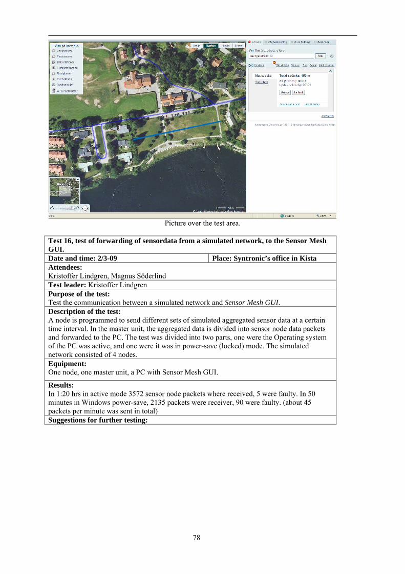
78
Picture over the test area.
Test 16, test of forwarding of sensordata from a simulated network, to the Sensor Mesh GUI. Date and time: 2/3-09 Place: Syntronic’s office in Kista Attendees: Kristoffer Lindgren, Magnus Söderlind Test leader: Kristoffer Lindgren Purpose of the test: Test the communication between a simulated network and Sensor Mesh GUI. Description of the test: A node is programmed to send different sets of simulated aggregated sensor data at a certain time interval. In the master unit, the aggregated data is divided into sensor node data packets and forwarded to the PC. The test was divided into two parts, one were the Operating system of the PC was active, and one were it was in power-save (locked) mode. The simulated network consisted of 4 nodes. Equipment: One node, one master unit, a PC with Sensor Mesh GUI.
Results: In 1:20 hrs in active mode 3572 sensor node packets where received, 5 were faulty. In 50 minutes in Windows power-save, 2135 packets were receiver, 90 were faulty. (about 45 packets per minute was sent in total) Suggestions for further testing: