Embed Size (px)
Citation preview
University of Central Florida University of Central Florida
STARS STARS
Electronic Theses and Dissertations, 2004-2019
2013
Development Of Polymer Derived Sialcn Ceramic And Its Development Of Polymer Derived Sialcn Ceramic And Its
Applications For High-temperature Sensors Applications For High-temperature Sensors
Gang Shao University of Central Florida
Part of the Materials Science and Engineering Commons
Find similar works at: https://stars.library.ucf.edu/etd
University of Central Florida Libraries http://library.ucf.edu
This Doctoral Dissertation (Open Access) is brought to you for free and open access by STARS. It has been accepted
for inclusion in Electronic Theses and Dissertations, 2004-2019 by an authorized administrator of STARS. For more
information, please contact [email protected].
STARS Citation STARS Citation Shao, Gang, "Development Of Polymer Derived Sialcn Ceramic And Its Applications For High-temperature Sensors" (2013). Electronic Theses and Dissertations, 2004-2019. 2690. https://stars.library.ucf.edu/etd/2690

DEVELOPMENT OF POLYMER DERIVED SIALCN CERAMIC
AND ITS APPLICATIONS FOR HIGH-TEMPERATURE
SENSORS
by
GANG SHAO
B.S. Zhengzhou University, China, 2006
M.S. Zhengzhou University, China, 2009
A dissertation submitted in partial fulfillment of the requirements
for the degree of Doctor of Philosophy
in the Department of Materials Science and Engineering
in the College of Engineering and Computer Science
at the University of Central Florida,
Orlando, Florida
Summer Term
2013
Major Professor: Linan An

ii
©2013 Gang Shao

iii
ABSTRACT
Polymer-derived ceramic (PDC) is the name for a class of materials synthesized
by thermal decomposition of polymeric precursors which excellent thermomechanical
properties, such as high thermal stability, high oxidation/corrosion resistance and high
temperature multifunctionalities. Direct polymer-to-ceramic processing routes of
PDCs allow easier fabrication into various components/devices with complex
shapes/structures. Due to these unique properties, PDCs are considered as promising
candidates for making high-temperature sensors for harsh environment applications,
including high temperatures, high stress, corrosive species and/or radiation.
The SiAlCN ceramics were synthesized using the liquid precursor of
polysilazane (HTT1800) and aluminum-sec-tri-butoxide (ASB) as starting materials
and dicumyl peroxide (DP) as thermal initiator. The as-received SiAlCN ceramics
have very good thermal-mechanical properties and no detectable weight loss and large
scale crystallization. Solid-state NMR indicates that SiAlCN ceramics have the SiN4,
SiO4, SiCN3, and AlN5/AlN6 units. Raman spectra reveals that SiAlCN ceramics
contain “free carbon” phase with two specific Raman peaks of “D” band and “G”
band at 1350 cm1
and 1600 cm1
, respectively. The “free carbon” becomes more and
more ordered with increasing the pyrolysis temperature. EPR results show that the
defects in SiAlCN ceramics are carbon-related with a g-factor of 2.0016±0.0006.
Meanwhile, the defect concentration decreases with increasing sintered temperature,
which is consistent with the results obtained from Raman spectra.
iv
Electric and dielectric properties of SiAlCN ceramics were characterized. The
D.C. conductivity of SiAlCN ceramics increases with increasing sintered temperature
and the activation energy is about 5.1 eV which higher than that of SiCN ceramics
due to the presence of oxygen. The temperature dependent conductivity indicates that
the conducting mechanism is a semiconducting band-gap model and follows the
Arrhenius equation with two different sections of activation energy of 0.57 eVand
0.23 eV, respectively. The temperature dependent conductivity makes SiAlCN
ceramics suit able for high temperature sensor applications. The dielectric properties
were carried out by the Agilent 4298A LRC meter. The results reveal an increase in
both dielectric constant and loss with increasing temperature (both pyrolysis and
tested). Dielectric loss is dominated by the increasing of conductivity of SiAlCN
ceramics at high sintered temperatures.
SiAlCN ceramic sensors were fabricated by using the micro-machining method.
High temperature wire bonding issues were solved by the integrity embedded method
(IEM). It’s found that the micro-machining method is a promising and cost-effective
way to fabricate PDC high temperature sensors. Moreover IEM is a good method to
solve the high temperature wire bonding problems with clear bonding interface
between the SiAlCN sensor head and Pt wires. The Wheatstone bridge circuit is well
designed by considering the resistance relationship between the matching resistor and
the SiAlCN sensor resistor. It was found that the maximum sensitivity can be
achieved when the resistance of matching resistor is equal to that of the SiAlCN

v
sensor. The as-received SiAlCN ceramic sensor was tested up to 600 C with the
relative output voltage changing from -3.932 V to 1.153 V. The results indicate that
the relationship between output voltage and test temperature is nonlinear. The tested
sensor output voltage agrees well with the simulated results. The durability test was
carried out at 510 C for more than two hours. It was found that the output voltage
remained constant for the first 30 min and then decreased gradually afterward by 0.02,
0.04 and 0.07 V for 1, 1.5 and 2 hours.

vi
ACKNOWLEDGMENTS
I would like to express my great gratitude to my advisor, Professor Linan An, for
his continuous encouragement and thoughtful guidance during my study at University
of Central Florida.
I would like to thank Professor Lee Chow, Professor Jiyu Fang, Professor
Chengying Xu, and Professor Weiwei Deng to contribute their time as my committee
members and all the valuable advices.
I would like to express my thank to Dr. Nina Orlovskaya, Dr. Yi Liao, Dr.
Chengying Xu, Dr. Lei Zhai, Dr. Zhongyang Chen for their help with the facilities
and results analysis.
I would like to thank Dr. Likai Song, Dr. Zhehong Gan and Mr. Lu Yu for EPR
and NMR test and analysis at National High Field Magentic Lab at Florida State
University.
I would like to acknowledge to Ms. Lujiao Yang, Dr. Yaohan Chen, Dr. Hongyu
Gong, Dr. Hongliang Xu, Dr. Wenge Li, Dr. Jianhua Zou, Ms. Xueping Yang, Mr.
Jinling Liu, Mr. Renan Gongora, Mr. Zhilin Xie, Ms. Zhen Shi, Dr. Feng Gao, Mr.
Douglas Freese, Mr. Anthony Spagnola for the help with my experiments and data
analysis.
I would like to give my specific thank to my families, my wife, Jingjing Wang,
my mother, Quanzhi Wang, my father, Yudong Shao, my sister, Xiuli Shao and my
brother, Feng Shao, for their encouragement and support all the time.
vii
TABLE OF CONTENTS
LIST OF FIGURES.............................................................................................................. ix
LIST OF TABLES ..............................................................................................................xiv
LIST OF ACRONYMS/ABBREVIATIONS ....................................................................... xv
CHAPTER ONE: INTRODUCTION .................................................................................... 1
1.1 Motivation ................................................................................................................... 1
1.2 Outline of dissertation.................................................................................................. 2
CHAPTER TWO: LITERATURE REVIEW ......................................................................... 3
2.1 Polymer-derived ceramics............................................................................................ 3
2.1.1 Polymeric precursors ............................................................................................ 4
2.1.2 Fabrication capability of polymer-derived ceramics............................................... 8
2.1.3 Microstructure of polymer-derived ceramics ....................................................... 11
2.1.4 Properties of polymer-derived ceramics .............................................................. 15
2.2 Background of high temperature sensors .................................................................... 28
References: ..................................................................................................................... 30
CHAPTER THREE: SiAlCN CERAMICS PREPARATION AND CHARACTERIZATION
........................................................................................................................................... 46
3.1 SiAlCN ceramics preparation..................................................................................... 46
3.1.1 Raw materials ..................................................................................................... 46
3.1.2 Experimental procedure ...................................................................................... 48
3.2 SiAlCN ceramics characterization, results and discussion .......................................... 50
3.2.1 Solid-state NMR ................................................................................................. 50
3.2.2 X-ray diffraction (XRD) ..................................................................................... 53
3.2.3 Electron paramagnetic resonance spectroscopy (EPR) ......................................... 54
3.2.4 Raman Spectroscopy ........................................................................................... 57
References: ..................................................................................................................... 62
CHAPTER FOUR: ELECTRIC AND DIELECTRIC PROPERTIES OF SiAlCN
CERAMICS ........................................................................................................................ 65
4.1 Experimental procedure ............................................................................................. 66

viii
4.2 Results and discussion ............................................................................................... 67
4.2.1 Electric properties of SiAlCN ceramics ............................................................... 67
4.2.2 Dielectric properties of SiAlCN ceramics ............................................................ 78
References: ..................................................................................................................... 89
CHAPER FIVE: HIGH TEMPERATURE SENSOR FABRICATION AND
CHARACTERIZATION ..................................................................................................... 90
5.1 Polymer derived SiAlCN sensor fabrication ............................................................... 91
5.2 Wheatstone bridge circuit design and analysis ............................................................ 93
5.3 SiAlCN ceramic sensor test and results discussion ................................................... 102
References: ................................................................................................................... 107
CHAPTER SIX: CONCLUSION ...................................................................................... 110
APPENDIX –A: CERAMIC NANOCOMPOSITES REINFORCED WITH HIGH VOLUME
FRACTION OF CARBON NANOFIBERS....................................................................... 113
APPENDIX- B: FABRICATION OF NANO-SCALED POLYMER DERIVED SIALCN
CERAMIC COMPONENTS USING FOCUSED ION BEAM .......................................... 131
ix
LIST OF FIGURES
Figure 2.1 Basic fabrication processing of PDCs. ........................................................... 4
Figure 2.2 Synthesis methods for polycarbosilazanes by using chlorosilanes as starting
materials5. .............................................................................................................. 5
Figure 2.3 Simplified general formula of the molecular structure of the Si-based
preceramic precursors6. .......................................................................................... 6
Figure 2.4 Main classes of preceramic polymer precursors for the fabrication of Si-based
PDCs6. ................................................................................................................... 6
Figure 2.5 Synthesis routes of polyaluminasilazanes starting from (CH3)3Al and
(CH3)2AlNH211
. ...................................................................................................... 7
Figure 2.6 Synthesis of polyaluminasilazanes by means of hydroalumination and
dehydrocoupling reactions12
. .................................................................................. 8
Figure 2.7 Fabrication methods of polymer-derived ceramics. ........................................ 9
Figure 2.8 3-D SiCN ceramic microstructures fabricated by nanostereolithography; (a)
schematically designed woodpile structure (b) polymeric structure without filler (c)
ceramic structure without filler & (d) ceramic structure with 20 wt% Si filler (e)
ceramic structure with 30 wt% Si filler (f) ceramic structure with 40 wt% Si filler,
and other 3-D microstructrues with 40wt% Si filler, (g) micro tube (h)
microcruciform. (Each inset is the top-view of the structure) 34
. ............................ 10
Figure 2.9 SiCN electrostatic actuator; (a) schematic drawn (b) assembled on a alumina
substrate15
. ........................................................................................................... 11
Figure 2.10 Schematic structure model of PDCs. ......................................................... 12
Figure 2.11 Raman spectroscopy of Si-SiCN mixture with the volume ratio of 1:1 (a). (b)
Plot of VSi/VSiCN as a function of normalized ISi/ICK44
. ........................................... 14
Figure 2.12 Thermal gravimetric analysis (TGA) of polymer-derived SiCN, SiBCN and
silicon nitride71
..................................................................................................... 17
Figure 2.13 Changes in the strain rate of SiBCN ceramic with time in three stage. At
1500oC and 75MPa
72. ........................................................................................... 17

x
Figure 2.14 A plot of the square of the oxide scale thickness as a function of annealing
time for both SiCN and SiAlCN at 1200C in dry air.[42] .................................... 18
Figure 2.15 SEM micrograph of the surface of (a) SiCN, (b) SiAlCN at 1400C for 300h
in 50%H2O-50%O2 environment83
........................................................................ 19
Figure 2.16 Model of carbon redistribution and continuous network formation of PPS
and PMS91
............................................................................................................ 20
Figure 2.17 Electric conductivity of SiCN ceramic depending on the annealing
temperature and time60
. ........................................................................................ 21
Figure 2.18 Temperature dependent conductivity of SiCNO ceramic up to 1300oC
93. ... 22
Figure 2.19 Electric conductivity of SiCNO ceramic varied with O/N ratio at room
temperature93
. ...................................................................................................... 22
Figure 2.20 The piezoresistive effect of SiCN ceramics (a) resistance change versus test
pressures (b) schematic drawing of conduction mechanism 95
. Insert figure is the
plot of guager factor versus tested pressure........................................................... 23
Figure 2.21 Polarization mechanisms in dielectric materials96
. ..................................... 25
Figure 2.22 ɛr, ɛrʹ and tanδ as a function of ω for cases with negligible contribution of s
due to carrier migration96
. .................................................................................... 26
Figure 2.23 Schematic diagram of ɛr-ɛrʹ relation for cases with only one relaxation time
τo96
. ...................................................................................................................... 27
Figure 3.1 The molecular formula of HTT1800. ........................................................... 47
Figure 3.2 The molecular formula of ASB. .................................................................. 47
Figure 3.3 The molecular formula of DP. ..................................................................... 47
Figure 3.4 Preparation procedure of SiAlCN ceramics. ................................................ 48
Figure 3.5 A schematic drawing of the sintering procedure of SiAlCN ceramics. ......... 49
Figure 3.6 29
Si solid-state NMR of SiAlCN ceramics sintered at 1000 C with different
ASB concentrations of 1, 5 and 10 wt% . ............................................................. 51
Figure 3.7 27
Al solid-state NMR of SiAlCN ceramics sintered at 1000 C with different
ASB concentration of 1, 5 and 10 wt% . ............................................................... 52

xi
Figure 3.8 XRD pattern of 10ASB2DP-SiAlCN ceramics sintered at 1400, 1500 C. ... 53
Figure 3.9 EPR spectra of SiAlCN ceramics sintered at 1000 C with different ASB
concentration of 1, 5 and 10wt%. ......................................................................... 55
Figure 3.10 EPR spectra of 10ASB2DP SiAlCN ceramics sintered at different
temperatures. ....................................................................................................... 56
Figure 3.11 Spin concentration of 10ASB2DP SiAlCN ceramics sintered at various
temperatures. ....................................................................................................... 56
Figure 3.12 Raman spectra of 10ASB-SiAlCN ceramics sintered at different
temperatures. ....................................................................................................... 58
Figure 3.13 D and G peak position of Raman spectra of 10ASB2DP SiAlCN ceramics
sintered at different temperatures.......................................................................... 59
Figure 3.14 FWHM of Raman spectra of 10ASB2DP SiAlCN ceramics sintered at
different temperature. ........................................................................................... 59
Figure 3.15 Intensity ratio of D and G (ID/IG) of Raman spectra of 10ASB2DP SiAlCN
ceramics sintered at different temperatures. .......................................................... 60
Figure 4.1 I-V curves and the curve fitting of SiAlCN ceramics sintered at different
temperature (a) 1000 C, (b) 1100 C, (c) 1200 C, (d) 1300 C, (e) 1400 C........ 67
Figure 4.2 Conductivity of SiAlCN ceramics sintered at different temperatures. ........... 68
Figure4.3 Schematic illustration of electric field concentration in SiAlCN system. ....... 69
Figure 4.4 Complex impedance analysis of SiAlCN ceramic sintered at different
temperatures (a) 1000 C, (b) 1200 C and (c) 1400 C. ....................................... 72
Figure 4.5 Plot of ln (conductivity) VS 1/T of SiAlCN and SiCN ceramics. ................. 73
Figure 4.6 XPS results of SiAlCN ceramics sintered at 1000 C. .................................. 74
Figure 4.7 Temperature dependent conductivity of SiAlCN and SiCN ceramics. .......... 75
Figure 4.8 Plot of ln (conductivity) VS 1/T of SiAlCN at different test temperatures. ... 77
Figure 4.9 Frequency dependence of dielectric constants for SiAlCN ceramics sintered at
different temperatures. ......................................................................................... 79

xii
Figure 4.10 Frequency dependence of dielectric loss of SiAlCN ceramics sintered at
different temperatures. ......................................................................................... 80
Figure 4.11 Dielectric constants of SiAlCN ceramics at specific frequency and various
sintered temperatures. .......................................................................................... 81
Figure 4.12 Dielectric loss of SiAlCN ceramics at specific frequency and various
sintered temperatures. .......................................................................................... 81
Figure 4.13 Schematic illustration of established space charge within SiAlCN system (a)
without electric field (b) with electric field ........................................................... 82
Figure 4.14 Dielectric loss of SiAlCN ceramics at specific frequencies and different
sintered temperatures. .......................................................................................... 84
Figure 4.15 Dielectric loss of SiAlCN ceramics at specific frequency and different
sintered temperatures. .......................................................................................... 85
Figure 4.16 Temperature dependent dielectric constant of SiAlCN ceramics sintered at
1000C. ............................................................................................................... 87
Figure 4.17 Temperature dependent dielectric loss of SiAlCN ceramics sintered at
1000C. ............................................................................................................... 87
Figure 4.18 Complex impendence analysis of SiAlCN ceramics at different tested
temperatures (a) 200 oC (b) 300
oC (c) 400
oC. ..................................................... 88
Figure 5.1 (a) SiAlCN ceramic sensor fabrication procedure and (b) optical image of
sensor. ................................................................................................................. 92
Figure 5.2 SEM images of Pt wire bonding of the ceramic sensor head. ....................... 93
Figure 5.3 A schematic drawing of a typical Wheatstone bridge circuit. ....................... 94
Figure 5.4 The sensor resistance changes with temperature (the imbedded plot shows the
high temperature range). ...................................................................................... 95
Figure 5.5 The plot of sensor resistance (ln(1/R) with inverse of the measured
temperature (T 1
). ................................................................................................ 96
Figure 5.6 Linear fitting of sensor resistance (ln(1/R)) versus measured temperature (T 1
)
at high temperature range. .................................................................................... 96
Figure 5.7 Plot of dR/dT VS test temperatures. ............................................................ 99
xiii
Figure 5.8 F(R3) changes with normalized R3/Rx at different sensor resistance Rx. .......... 99
Figure 5.9 Maximum F(R3) change with different sensor resistances Rx. ...................... 100
Figure 5.10 The maximum sensitivity dV/dT at different temperatures (Vin = 5 V). .... 100
Figure 5.11 Simulated sensitivity dV/dT at various test temperatures (R3=30 MΩ Vin =
5V). ................................................................................................................... 101
Figure 5.12 Calculated sensor output voltage versus temperature (R3=30 MΩ, Vin= 5 V,
R1=R2). .............................................................................................................. 102
Figure5.13 SiAlCN sensor test set up and Wheatstone bridge circuit. ......................... 103
Figure5.14 SiAlCN ceramic sensor output voltage and thermal couple reading VS time.
.......................................................................................................................... 104
Figure 5.15 SiAlCN ceramic sensor output voltage (simulated and tested results)....... 105
Figure5.16 Durability test of SiAlCN ceramic sensor. ................................................ 106
xiv
LIST OF TABLES
Table 2.1 Properties of polymer derived SiCN and other high-temperature materials. ... 19
Table 3.1 Composition design of SiAlCN ceramics ...................................................... 49
Table 3.2 Carbon cluster size (La) of 10ASB2DP SiAlCN ceramics sintered at different
temperatures ........................................................................................................ 61
Table 4.1 Conductivities of SiAlCN and SiCN sintered at various temperatures. .......... 68
Table 4.2 Dielectric constants and loss of SiAlCN ceramics at different sintered
temperatures and frequencies. .............................................................................. 80
Table 4.3 Slops of the linear fit of logarithm of the imaginary part of the dielectric
constant and the logarithm of frequency of 10ASB2DP-SiAlCN ceramics. ........... 85
xv
LIST OF ACRONYMS/ABBREVIATIONS
ASB Aluminum tri-sec-butoxide
CVD Chemical vapor deposition
DP Dicumyl peroxide
EELS Electron Energy Loss Spectroscopy
FIB Focused iron beam
IEM Integrity embed method
MEMS Micro-electro-mechanical systems
NMR Nuclear magnetic resonance
PDC Polymer Derived Ceramics
SAXS Small Angle X-ray Scattering
SEM Scanning electron microscopy
TEM Transformation Electron Microscopic
TGA Thermogravimetric analysis
XRD X-ray diffraction

1
CHAPTER ONE: INTRODUCTION
1.1 Motivation
Temperatures must be monitored to prevent damage of devices and improve
their performance in high temperature and harsh environments, such as gas
turbines, nuclear reactors, high speed vehicles and automotives. Therefore, robust
sensors are highly desired in the harsh environment of high temperature, high
pressure, oxidation, radiation and corrosive species. Sensors that can be applied in
these hostile applications must satisfy two features: firstly, the sensor materials
must survive at these environments; secondly, the materials must maintain
specific properties by means of sensoring. Most of the current available materials
are excluded by these two requirements. Currently, several techniques are under
development for such applications. However, present electronics technologies are
limited to silicon-based technology, which has a limited operating temperature
range of a few hundred degrees Celsius and is not suitable for high temperature
sensing applications. Another possible option is using the refractory materials,
such as silicon carbide and/or silicon nitride. However, these type of sensors are
very restricted by limited fabrication methods, high cost, and a limited operation
temperature range (typically < 800 C), especially if the environment involves
corrosive atmospheres as well.
Recently, polymer-derived ceramics (PDCs) have been considered as suitable
materials for making high-temperature microelectromechanical systems

2
(MEMS)/micro-sensors, because PDCs exhibit excellent thermomechanical
properties, such as high thermal stability, high oxidation/corrosion resistance and
high temperature multifunctionalities. In addition, the direct polymer-to-ceramic
processing route of PDCs makes it much easier to be fabricated into various
components/devices with complex shapes/structures.
The overall objective of this dissertation is to develop a suitable micro-scaled
temperature sensor which can fulfill the requirements of operating in high
temperature and harsh environment for online, real-time temperature measuring
and health monitoring.
1.2 Outline of dissertation
The dissertation is organized by the following parts:
Chapter 2 is the literature review of the background of polymer derived
ceramics and their unique properties suitable for high temperature application.
The fabrication and characterization of SiAlCN ceramics is discussed in Chapter 3.
Chapter 4 focuses on the electric and dielectric properties of SiAlCN ceramics.
Chapter 5 includes the SiAlCN ceramic sensor fabrication and characterization.
Chapter 6 contains the general conclusions of this dissertation. Additionally,
Appendix I and Appendix II illustrated the nanofabrication capability of SiAlCN
ceramics by using focused iron beam (FIB) and the application of SiAlCN
ceramics in forming carbon nanofiber reinforced ceramic nanocomposites.
3
CHAPTER TWO: LITERATURE REVIEW
This chapter is separated into two main sections (1) background information of
polymer-derived ceramics (PDCs) and (2) high temperature sensors. The first part
includes preceramic precursors, fabrication and processing techniques,
microstructures and properties of PDCs. The second part discusses different high
temperature sensors, materials/devices, including resistance temperature detectors,
thermistors and PDCs sensors.
2.1 Polymer-derived ceramics
Polymer-derived ceramics (PDCs) are a class of materials synthesized by thermal
decomposition of polymeric precursors. The basic processing of PDCs is illustrated in
Figure 2.1, including the following steps: (i) synthesis of precursors from starting
chemicals, (ii) crosslinkage of the precursor into an infusible preceramic network, and
(iii) pyrolysis of the preceramic network into ceramics. PDCs provide advantages,
such as, flexible fabrication capability, low sintering temperature and excellent
oxidation and creep resistance compared to the traditional powder route ceramics.
After pyrolysis, the ceramics are predominately amorphous and this structure can be
retained even up to high temperatures. Further increasing temperature may lead to
crystallization of the amorphous structure to form polycrystalline ceramics. The
majority of researches on PDCs have been focused on amorphous state.

4
Figure 2.1 Basic fabrication processing of PDCs.
2.1.1 Polymeric precursors
PDCs have attracted great attention in these last few decades due to their
promising high temperature harsh environment applications. Many types of PDCs
have been discovered and can be classified into three main types, based on the
number of the components in the system, (1) binary systems of SiC, and Si3N4, (2)
ternary systems of SiCN, SiCO and BCN as well as (3) quaternary and multinary
systems of SiAlCN, SiCNO, SiBCN and SiAlBCN, SiBCNO and so on.
One key issue for developing polymer-derived ceramics (PDCs) is to
synthesize precursors, the starting material, to obtain PDCs. Composition,
microstructure and the properties of PDCs are all influenced by the starting material
used. In the 1960’s, the first publications that use the fabrication of polymer-derived
ceramics were reported by Ainger1 and Chantrell
2. After that several research groups
worked on synthesis PDCs. However, PDCs were not fully recognized until Yajima3
and Fritz4 synthesized SiC and Si3N4 ceramic fibers, crucial in the fields of aerospace,
military and energy propulsion.
Organosilicon polymers are the most widely used stating materials due to their
well know chemistry, reaction-controlled thermolysis and polymerized function sites
including the following functional groups: Si-H, Si-Cl, Si-C=C. The synthesis of
preceramic percursors are commonly utilizes chlorosilanes RxSiCl4-x (x=0-3) for use

5
as starting materials. Normally through two kinds of methods of ammonolysis
reactions with ammonia or aminolysis with different amines5 we can obtain the
desired chlorosilane, as illustrated in Figure 2.2. Various types of precursors were
synthesized by using silicon-based polymers, such as, polysilanes, polysilazanes,
polysiloxanes, polycarbosilanes, polyborosilazanes and polyaluminasilazanes.
Figure 2.2 Synthesis methods for polycarbosilazanes by using chlorosilanes as
starting materials5.
Most recently, Colombo and his co-workers summarized a simplified general
formula of Si-based precursor as shown in Figure 2.36. As we can see there are two
important parameters of this general formula: the backbone group X and the
functional group R1 and R
2. The type of Si-based polymeric precursor is determined
by the backbone group X, for example, if X = Si then we obtain poly(organosilanes);
if X = O then we obtain poly(organosiloxanes); if X = B then we obtain poly
(organoborosilazanes); if X = CH2 then we obtain poly(organocarosilanes) and if X=
NH then we obtain poly(organosilazanes). More and more combinations are
illustrated in Figure 2.46. The functional group R
1 and R
2 (either hydrogen, aliphatic
or aromatic side groups) are highly related to composition, microstructure and
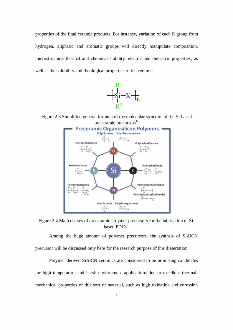
6
properties of the final ceramic products. For instance, variation of each R group from
hydrogen, aliphatic and aromatic groups will directly manipulate composition,
microstructure, thermal and chemical stability, electric and dielectric properties, as
well as the solubility and rheological properties of the ceramic.
Figure 2.3 Simplified general formula of the molecular structure of the Si-based
preceramic precursors6.
Figure 2.4 Main classes of preceramic polymer precursors for the fabrication of Si-
based PDCs6.
Among the huge amount of polymer precursors, the synthsis of SiAlCN
precursor will be discussed only here for the research purpose of this dissertation.
Polymer derived SiAlCN ceramics are considered to be promising candidates
for high temperature and harsh environment applications due to excellent thermal-
mechanical properties of this sort of material, such as high oxidation and corrosion

7
resistance, high temperature stability and multifunctionality. Several SiAlCN
precursors were reported such as, {[(Me3Si)2N]2AlNH2}27, (Et2AlNH2)3
8,
(CH3)2AlNH29
and (Al(OCH(CH3)2)310
. The high yield SiAlCN precursor was
synthesized by reacting the polysilazane [CH3HNH]n either with (CH3)3Al or
(CH3)2AlNH2 reported by Seyferth and co-workers9
as shown in Figure 2.5. With
respect to synthesis, they also found that the (CH3)2AlNH2 is a better choice than
(CH3)3Al due to the lower alkylating activity and presence of crosslinkable Al-NH2
groups. Berger11
prepared polyaluminasilazanes from polysilazanes and
polysilylcarbodiimides by means of hydroalumination of vinyl substituents at Si and
subsequent dehydrocoupling of N-H reactive sites, as demonstrated in Figure 2.6. The
detailed polymer-to-ceramic evolution during the pyrolysis was investigated by
Dhamne and co-workers12
.
Figure 2.5 Synthesis routes of polyaluminasilazanes starting from (CH3)3Al and
(CH3)2AlNH211
.

8
Figure 2.6 Synthesis of polyaluminasilazanes by means of hydroalumination and
dehydrocoupling reactions12
.
2.1.2 Fabrication capability of polymer-derived ceramics
One unique advantage of PDCs is its flexible processing capability for making
ceramic components/devices with complex and inconvenient shapes due to the
intermediate state of the liquid polymer, which the traditional ceramic-powder route
cannot. A variety of ceramic component/devices, such as high-temperature ceramic
fibers, ceramic matrix composites, micro-electro-mechanical systems (MEMS) and
micro-sensors, have been fabricated by using PDC processing. These
components/devices are particularly important for applications in harsh environments
with high temperature and corrosion.
The as-synthesized liquid polymeric precursor can be easily shaped into various
complex structures/components. These shaping techniques could be casting
(micro/nano casting13-15
, tape casting16
and freeze casting17
), machining18
, lithography
(soft lithography19-21
and microstereolithography22
), coating (spraying coating23
, dip
coating24,25
, spin coating26
and chemical vapor deposition27
), fiber drawing28,29
and

9
direct writing30
as well as fabrication of composites31-33
. A schematic drawing of the
fabrication techniques was included in Figure 2.7.
Figure 2.7 Fabrication methods of polymer-derived ceramics.
Pham and co-workers34
fabricated 3-D SiCN ceramic nanostructures with a
resolution of 210nm, and found the addition of Si-nanoparticle fillers may greatly
reduce shrinkage to get integrated features as shown in Figure 2.8.
20 m
Fibers
40 m
Composites
541 nm
Coating
1 m
Nanostructures
1 cm
Bulk components
200 m
MEMS
Polymer precursor route:
Organics to ceramics
20 m
FibersFibers
40 m
CompositesComposites
541 nm
CoatingCoating
1 m
NanostructuresNanostructures
1 cm
Bulk componentsBulk components
200 m
MEMSMEMS
Polymer precursor route:
Organics to ceramics

10
Figure 2.8 3-D SiCN ceramic microstructures fabricated by nanostereolithography; (a)
schematically designed woodpile structure (b) polymeric structure without filler (c)
ceramic structure without filler & (d) ceramic structure with 20 wt% Si filler (e)
ceramic structure with 30 wt% Si filler (f) ceramic structure with 40 wt% Si filler, and
other 3-D microstructrues with 40wt% Si filler, (g) micro tube (h) microcruciform.
(Each inset is the top-view of the structure) 34
.
The flexibility of fabrication of micro-electro-mechanical systems (MEMS) and
micro sensor/actuator/transducer of PDCs has allowed increased investigations by
other research groups. Liew and co-workers 15,35-38
at the University of Colorado at
Boulder USA, fabricated a series of SiCON MEMS devices by using preceramic

11
polymers and photolithography methods. They prepared a vertical electrostatic
actuator which consisted a four-flexured SiCN structure mounted onto a alumina
substrate with metal pads and wiring shown in Figure 2.9. The thickness of SiCN was
40 μm and suspended 3μm above the electrode and a deflection of 370nm was
detected coresponding to the input voltage of 200V.
Figure 2.9 SiCN electrostatic actuator; (a) schematic drawn (b) assembled on a
alumina substrate15
.
2.1.3 Microstructure of polymer-derived ceramics
Amorphous PDCs possess very complex structures different from
conventional crystalline and amorphous structures. While the exactly structures of
PDCs are not known very well which depends on the composition of the precursor,
pyrolysis conditions and annealing temperatures. As stated earlier, PDCs are
composed of an amorphous matrix made of SiCxN4-x (x can be 0, 1, 2, 3 and 4) units
and free carbon phase which forms nano-sized clusters. In addition, the materials
contain a fairly large amount of carbon dangling bonds, which are either in the matrix
or on the surface of the carbon nanoclusters. The schematic structure model of PDCs
(a) (b)
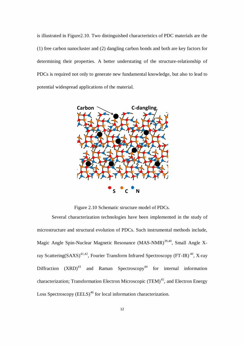
12
is illustrated in Figure2.10. Two distinguished characteristics of PDC materials are the
(1) free carbon nanocluster and (2) dangling carbon bonds and both are key factors for
determining their properties. A better understating of the structure-relationship of
PDCs is required not only to generate new fundamental knowledge, but also to lead to
potential widespread applications of the material.
Figure 2.10 Schematic structure model of PDCs.
Several characterization technologies have been implemented in the study of
microstructure and structural evolution of PDCs. Such instrumental methods include,
Magic Angle Spin-Nuclear Magnetic Resonance (MAS-NMR)39,40
, Small Angle X-
ray Scattering(SAXS)41,42
, Fourier Transform Infrared Spectroscopy (FT-IR) 40
, X-ray
Diffraction (XRD)43
and Raman Spectroscopy44
for internal information
characterization; Transformation Electron Microscopic (TEM)45
, and Electron Energy
Loss Spectroscopy (EELS)46
for local information characterization.
Carbon
cluster
S
i
C N
C-dangling
bond

13
As mentioned above, the microstructure of PDCs includes two main parts, the
amorphous matrix and free carbon cluster, therefore, the structural characterization
and evolution of PDCs will be discussed in this section with respect to these two parts.
Raman spectroscopy is a powerful and nondestructive tool for the initial
examination of carbon materials. As of today, the Raman spectroscopy is widely used
to characterization the structure evolution of free carbon in PDCs47-50
. Two major
Raman peaks of free carbon are observed in PDCs; the first peak corresponding to the
D bond at approximately 1350 cm-1
and the second peak corresponding to the G bond
at approximately 1582 cm-1
as well as the D’- and G’ bonds located at ~ 1620 cm-1
and 2700 cm-1
, respectively50
. The G bond is caused by in-plane bond stretching of
sp2 carbon, which is very important for the electric properties of PDC. Another
important parameter that needs to be considered is the intensity ratio between D bond
and G bond (ID/IG). This ratio can be used to calculate the free carbon cluster size.
Due to the crucial role that free carbon plays in the determination of the
properties of PDCs quantitative measurement must be done in order to reveal the
concentration of free carbon. This quantitative analysis of free carbon content in SiCN
system can be revealed by Raman spectroscopy reported by Jiang and co-workers44
.
They used silicon powder as an external reference, as shown in Figure 2.11 (a). A
linear relationship between the volume ratio of silicon powder, SiCN powder
(VSi/VSiCN) and normalized intensity ratio of (ISi/ICK) was found. Therefore, the free
carbon concentration was achieved as the slope of the plot of VSi/VSiCN versus ISi/ICK,
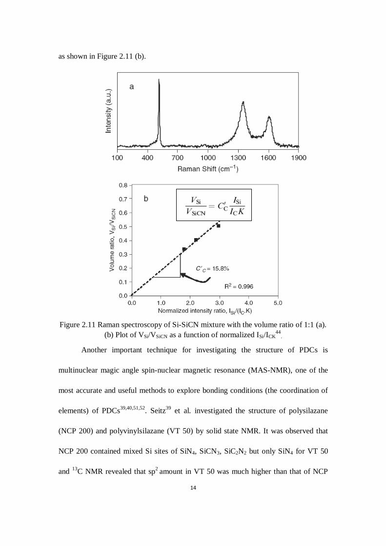
14
as shown in Figure 2.11 (b).
Figure 2.11 Raman spectroscopy of Si-SiCN mixture with the volume ratio of 1:1 (a).
(b) Plot of VSi/VSiCN as a function of normalized ISi/ICK44
.
Another important technique for investigating the structure of PDCs is
multinuclear magic angle spin-nuclear magnetic resonance (MAS-NMR), one of the
most accurate and useful methods to explore bonding conditions (the coordination of
elements) of PDCs39,40,51,52
. Seitz39
et al. investigated the structure of polysilazane
(NCP 200) and polyvinylsilazane (VT 50) by solid state NMR. It was observed that
NCP 200 contained mixed Si sites of SiN4, SiCN3, SiC2N2 but only SiN4 for VT 50
and 13
C NMR revealed that sp2
amount in VT 50 was much higher than that of NCP

15
200. Widgeon52
and colleges used high-resolution NMR to reveal the structure of
SiCO-PDC which consisted of a SiCxO4-x network and a sp2 hybrid free carbon
nanodomain. At the same time, the oxygen-rich SiCxO4-x units were expected to be
more concentrated in the interior of this network while the carbon-rich units were
expected to be localized at the interface of free carbon nanodomains.
Electron paramagnetic resonance (EPR) is yet another widely used technique
to characterize the structure of PDC. EPR was used to determine the type of defects
and their concentration in PDCs40,53-55
. Sergey54
and co-workers found that the EPR
signals of SiCN ceramics corresponded to dangling sp2 hybridized carbon within the
temperature range of 4 to 300K with g factor of 2.0027. Decreasing line width was
noticed with increasing pyrolysis temperature. Yee55
et al. characterized the SiBN and
SiBCN system using EPR spectrum and revealed that the EPR signals of SiBN were
very weak and in contrast, that of SiBCN were much stronger. They believed that
because the later one introduced carbon in the network. The trend of intensity of EPR
according to pyrolysis temperatures varied case by case due to precursor
differences53,55
.
2.1.4 Properties of polymer-derived ceramics
Numerous publications reported about different properties of PDCs, such as
mechanical properties56-59
, electric properties60-62
, thermal-mechanical properties63-66
,
optical67,68
and magnetic properties69,70
. In this section, only the thermal-mechanical,

16
electric and dielectric properties will be discussed for high temperature sensor
applications.
2.1.4.1 Thermal-mechanical properties of PDCs
PDCs possess excellent thermal-mechanical properties of high
oxidation/corrosion resistance, high temperature stability, high creep resistance. These
excellent high temperature properties make PDCs promising candidates for the high
temperature harsh environment applications. Ralf71
and co-workers developed a
SiBCN ceramic with very high temperature stability. They did not find any serious
thermal decomposition up to 2000oC which high than that of SiCN and Si3N4
ceramics and suggested application exceed to 1500oC, as shown in Figure 2.12. The
materials did not show large-scale crystallization up to 1600-1700oC. Long time
durability is another important feature for high temperature applications. The high
temperature experiment had been carried out on polymer derived ceramics72-74
and the
results revealed that the SiBCN ceramics had a negligible strain rate at the
temperature as high as 1500oC (Figure 2.13).
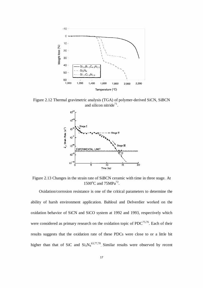
17
Figure 2.12 Thermal gravimetric analysis (TGA) of polymer-derived SiCN, SiBCN
and silicon nitride71
.
Figure 2.13 Changes in the strain rate of SiBCN ceramic with time in three stage. At
1500oC and 75MPa
72.
Oxidation/corrosion resistance is one of the critical parameters to determine the
ability of harsh environment application. Bahloul and Delverdier worked on the
oxidation behavior of SiCN and SiCO system at 1992 and 1993, respectively which
were considered as primary research on the oxidation topic of PDC75,76
. Each of their
results suggests that the oxidation rate of these PDCs were close to or a little bit
higher than that of SiC and Si3N463,77,78
. Similar results were observed by recent

18
researchers64,79
and even for the B-doped PDC80
. Most recently, Wang and An
revealed that the Al-doped SiCN ceramics had a higher oxidation resistance than that
of the above mentioned ceramics66,81-85
. They found that the oxidation thickness of
SiAlCN was much smaller than that of SiCN at the same oxidation time with the
tested temperature of 1200oC. And after 100 hours the oxidation thickness of SiAlCN
tended to achieve steady state, in contrast, that of SiCN kept increasing, as shown in
Figure 1.14. It was reported that SiAlCN ceramics had excellent corrosion resistance
than SiCN ceramics which were comparable with SiC and Si3N483
, as illustrated of the
SEM images in Figure 2.15. The properties of polymer derived ceramics and other
high-temperature materials are compared in Table 2.1. It shows that polymer derived
ceramics have much better oxidation resistance than others. The oxidation/corrosion
is one of the most important problems to limit the high temperature applications of
materials. Due to the high oxidation/corrosion resistant of SiAlCN ceramics, they are
good candidates for high temperature and harsh environment applications.
Figure 2.14 A plot of the square of the oxide scale thickness as a function of
annealing time for both SiCN and SiAlCN at 1200C in dry air.[42]

19
Figure 2.15 SEM micrograph of the surface of (a) SiCN, (b) SiAlCN at 1400C for
300h in 50%H2O-50%O2 environment83
.
Table 2.1 Properties of polymer derived SiCN and other high-temperature
materials.
SiCN SiC Si3N4
Density (g/cm3) (annealed @ 1000C) 2.2 3.17 3.19
Young’s modulus (GPa) 92 400 320
Poisson’s ratio 0.18 0.14 0.24
CTE (106/K) 3 3.8 2.5
Strength (MPa) ~500-
1000 ~400 ~700
Hardness (GPa) 15-20 30 28
Fracture toughness (MPam1/2
) 2-3.5 4-6 5-8
Thermal shock FOM* 1800-
3600 350 880
Oxidation rate (10-18
m2/s, @ 1400C) 0.47 16.4
77# 6.2
78#
Corrosion rate (10-6
g/cm2hr, @ 1400C
in water vapor) 0.98 6.4
86# 6.2
18#
* Thermal shock FOM = strength/(E.CTE)
# The lowest values reported for SiC and Si3N4 tested at the same conditions.
2.1.4.2 Electric properties of PDCs
Previous studies have shown that polymer derived ceramics are one kind of
amorphous semiconductors and their electric conductivities can be tailored within a
large range up to 15 orders of magnitude (typically from ~10-10
to ~1 (ohm*cm)-1
) by
varying the polymeric precursor, pyrolysis temperature and atmosphere as well as the
annealing temperature and time36,60,87-90
. For example, PDCs behave more like a
20
insulator at low pyrolysis temperature < 600oC, and semiconductor at middle
temperatures < 1200~1400oC, when goes to high sintered temperature > 1400
oC,
they are can be described as metal semiconductors. Researchers also found that free
carbon plays an important role to determine the electric properties of PDCs47,89
. The
free carbon will form a continuous network and contribute the overall conductivity of
the PDCs when increasing the pyrolysis temperature. However, these formation
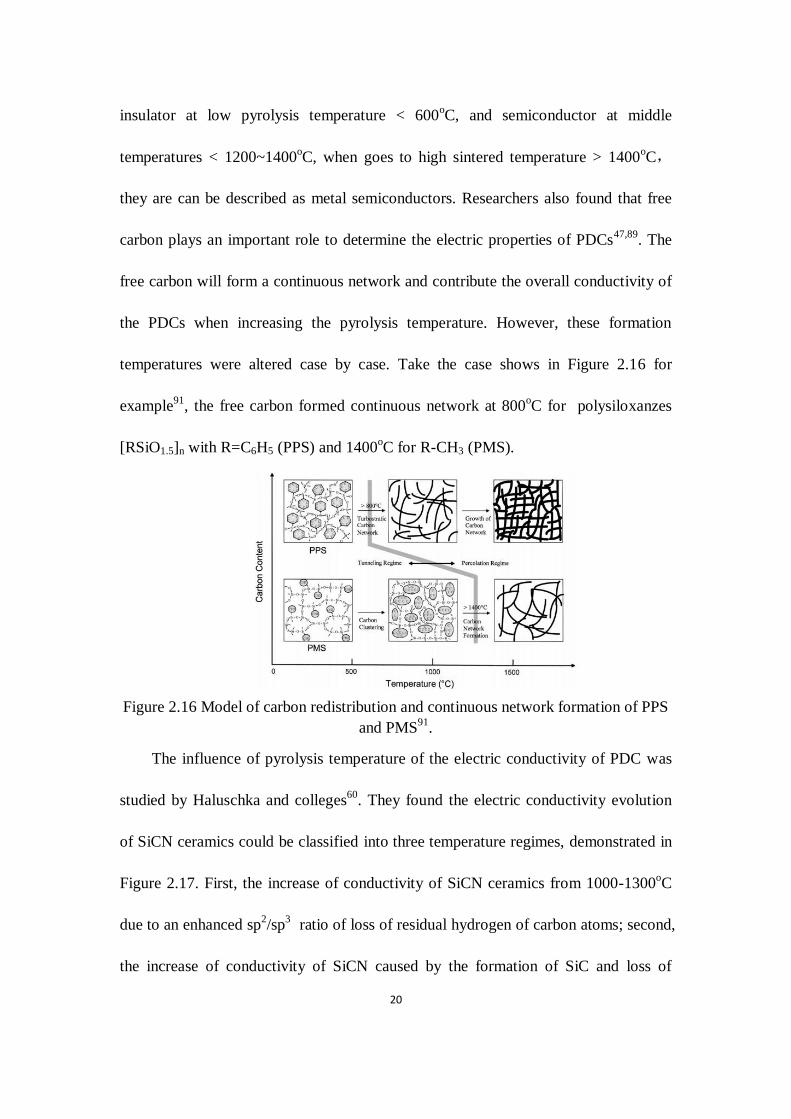
temperatures were altered case by case. Take the case shows in Figure 2.16 for
example91
, the free carbon formed continuous network at 800oC for polysiloxanzes
[RSiO1.5]n with R=C6H5 (PPS) and 1400oC for R-CH3 (PMS).
Figure 2.16 Model of carbon redistribution and continuous network formation of PPS
and PMS91
.
The influence of pyrolysis temperature of the electric conductivity of PDC was
studied by Haluschka and colleges60
. They found the electric conductivity evolution
of SiCN ceramics could be classified into three temperature regimes, demonstrated in
Figure 2.17. First, the increase of conductivity of SiCN ceramics from 1000-1300oC
due to an enhanced sp2/sp
3 ratio of loss of residual hydrogen of carbon atoms; second,
the increase of conductivity of SiCN caused by the formation of SiC and loss of

21
nitrogen of amorphous matrix between 1300 and 1600oC; third, the electric
conductivity was contributed by nitrogen doped SiC.
Figure 2.17 Electric conductivity of SiCN ceramic depending on the annealing
temperature and time60
.
Researchers tested the temperature dependence conductivity properties in order
to understand the conduction mechanism of amorphous PDCs 60,88,92
. The mechanisms
were found and is probable that three dimension variable range hopping (Mott’s law)
with a linear relationship between the conductivity of T1/4
(Equation 2.1, T is testing
temperature), band-gap semiconducting mechanism which follows Arrhenius law
with a linear relationship of conductivity and inverse test temperature (Equation 2.2)
as well as the band tail hopping mechanism. Most recently, Ryu and colleges93
found
the semiconducting behavior of SiCNO ceramics are able to sustain temperatures up
to 1300oC which is the highest one among all reported ceramic materials. The
conducting mechanism of these materials was variable range hopping and the electric
conductivity was highly depending on the O/N ratio, as shown in Figure 2.18 and
Figure 2.19.

22
14
00 exp
T
T
Eq. (2-1)
0 expE
kT
Eq. (2-2)
Currently, Zhang et al. discovered a super high piezoresistivity effect of SiCN
ceramic with a gauge factor as high as 1000~400094
which is much higher than that of
any existing ceramics (Figure 2.20 (a)). The mechanism was due to the formation of
tunneling percolation effect of free carbon as shown in Figure 2.20 (b)95
.
Figure 2.19 Electric conductivity of
SiCNO ceramic varied with O/N ratio
at room temperature93
.
Figure 2.18 Temperature
dependent conductivity of SiCNO
ceramic up to 1300oC
93.
(a) (b)

23
Figure 2.20 The piezoresistive effect of SiCN ceramics (a) resistance change versus
test pressures (b) schematic drawing of conduction mechanism 95
. Insert figure is the
plot of guager factor versus tested pressure.
2.1.4.3 Dielectric properties of PDCs
A brief summary of the background of dielectric theory will first be addressed
because it is not as mature as classical theories of electricity and mechanics.
Dielectrics are a class of materials that can respond to an external electric
stimulation with a polarization and have been widely used in industries as capacitors,
resonators and energy storage devices. The polarization P is proportional to the
electric field E.
0P E Eq. (2-3)
where χ is a constant, named dielectric susceptibility and ɛo is the dielectric constant
in vacuum (8.85×10¹²
F/m).
The dielectric constant is a measure of the polarization capability of a material.
The definition of complex dielectric constant is
(b)

24
* 'jr r Eq.(2-4)
where j is the image unit; ɛr and ɛʹ are the real part and image part of the dielectric
constant, respectively. Meanwhile, the dielectric loss is defined as
'
tan r
r
Eq. (2-5)
where δ is loss angle.
Polarization is one of the most important parameters to understand in
dielectrics. Generally, there are five polarization mechanisms for a dielectric material,
as shown in Figure2.2196
.
1) Electronic polarization: electric field induced displacement of the outer electron
cloud with respect to the inner positive nuclei. The response time is usually
~1014
-1016
s.
2) Atomic or ionic polarization: The distance between the positive charged atoms
and negative charged atoms can be changed by an electric field. The response
time is ~1012
-1013
s.
3) Orientational polarization: If there are dipoles in a material, the electric field
generates a torque on each dipole, which causes dipoles aligned along the electric
field direction. The response time is ~100-10
9s (which highly dependents on
temperature).

25
4) Hopping polarization: localized charges (ions and vacancies, or electrons and
holes) can hop from one site to the neighboring site under an electric field. The
response time is ~102
-105
s (which highly dependents on temperature).
5) Space charge polarization: The mobile or trapped charges (positive and negative
charged) can be separated by an electric field. The response time is ~102-10
1s.
(highly dependents on temperature).
Figure 2.21 Polarization mechanisms in dielectric materials96
.
The Debye theroy is the most well-known and useful theroy for understanding
dielectric phenoment of materials. The Debye equation is described as following and
the schematic drawn is illustrited in Figure 2.22.
* '
0
j1 j
rsr r r
Eq. (2-6) (1)
2 2
01 j
rs rr r
Eq. (2-6) (2)
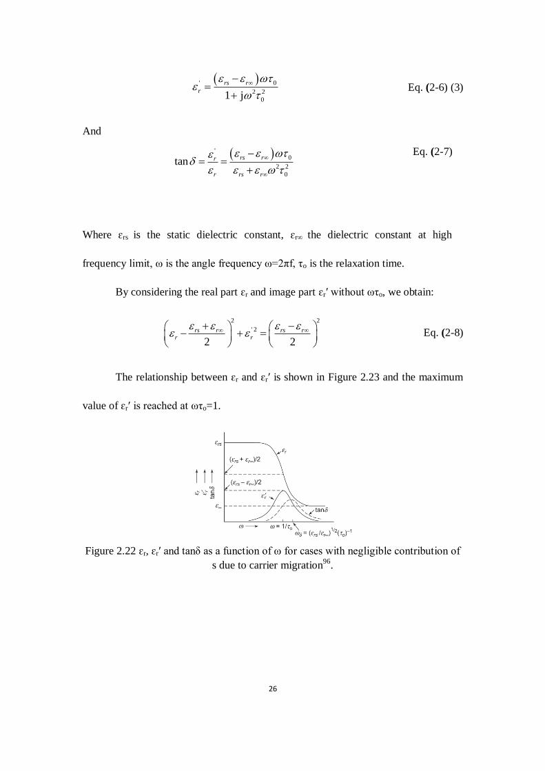
26
0'
2 2
01 j
rs r
r
Eq. (2-6) (3)
And
'0
2 2
0
tanrs rr
r rs r
Eq. (2-7)
Where ɛrs is the static dielectric constant, ɛr∞ the dielectric constant at high
frequency limit, ω is the angle frequency ω=2πf, τo is the relaxation time.
By considering the real part ɛr and image part ɛrʹ without ωτo, we obtain:
2 2
' 2
2 2
rs r rs rr r
Eq. (2-8)
The relationship between ɛr and ɛrʹ is shown in Figure 2.23 and the maximum
value of ɛrʹ is reached at ωτo=1.
Figure 2.22 ɛr, ɛrʹ and tanδ as a function of ω for cases with negligible contribution of
s due to carrier migration96
.

27
Figure 2.23 Schematic diagram of ɛr-ɛrʹ relation for cases with only one relaxation
time τo96
.
The state of art of dielectric properties of polymer derived ceramics.
The studies of dielectric properties of PDCs are very limited. Jiang97
characterized the dielectric constant and loss of SiCN ceramics and found that the
SiCN owned a very high dielectric constant and loss due to the high defect
concentration and free carbon content. Similar results were also found by Yu98
and
Li99
in SiCTi and SiBCN system, respectively. Recently, Ren and colleges100,101
used
a dielectric resonator cavity method measured the dielectric properties of SiBCN
ceramic at microwave frequency and high temperature. The dielectric constant and
loss increased with increasing test temperature.
Due to the unique properties of flexible near net sharp fabrication capability,
high oxidation/corrosion resistance, high temperature stability and multifunction
properties, polymer derived ceramics are considered promising candidates for high
temperature and harsh environment applications.
28
2.2 Background of high temperature sensors
Turbine engines can be found in power generation systems, aerospace
propulsion, and automotives and are important to the functionality of such systems.
The working condition of turbine engine system is very hostile include high
temperatures (500-1400C), high pressures (200-600 psi), and corrosive environments
(oxidizing conditions, gaseous alkali, and water vapors). Online, real-time
temperature and pressure monitoring of the inert environment of turbine engines can
further improve the performance and reliability, reduce the pollution and improve the
turbine engines design. Robust sensors are highly desired to measure and monitor the
temperature and pressure in these harsh environments. However, fabrication of such
sensors presents a huge technical challenge. The major hurdle is that the sensors must
survive harsh environments, including high temperatures, high stress, corrosive
species and/or radiation. In addition, the sensor materials must maintain specific
properties at high temperatures in order to provide means for sensing; and they must
do so in an easy-to-microfabricate way in order to lower costs.
Currently, several techniques are under development for such applications.
High temperature metal based resistance temperature detector (RTD), such as Pt. This
kind of sensor is very expensive and plagued with problems of self heating, long
response time and bad oxidation/corrosion resistance as well as limited working
temperature <550oC for most applications. Optical-based non-contact technology is a
popular method in determining these parameters. However, it has been shown to lack

29
the necessary accuracy for good measurement and typically break down over
time102,103
. Another promising technique to measure these parameters without
disturbing the work environment is using miniature sensors. Silicon carbide (SiC) and
silicon nitride (Si3N4)-based ceramic microsensors are being investigated for high-
temperature and harsh environment applications104-108
. However, these sensors are
very restricted by limited fabrication methods, high cost, and a limited operation
temperature range (typically < 800oC).
Most recently, polymer derived ceramics have attracted a great deal of
attention for making high temperature sensors due to their excellent high temperature
properties. Leo and colleges109
proposed a hybrid SiCN high temperature pressure
sensor by embedding piezoresistive chromium strain gauge between two thin SiCN
membranes. Seo and co-workers110
demonstrated a fabrication method of PDCs thin
films for high temperature heat flux sensor application. However, these “PDC sensors”
are all at a early stages of development and are currently at the conceptual level; no
real sensors have been fabricated and characterized at the current moment.

30
References:
1. Herbert, F. W. A. a. J. M. 168-182 (Academic press, New York, 1960).
2. Popper, P. G. C. a. P. (ed P. Popper) 87-103 (Academic Press, New York,
1965).
3. Yajima, S., Hasegawa, Y., Okamura, K. & Matsuzawa, T. Development of
high tensile strength silicon carbide fibre using an organosilicon polymer
precursor. Nature 273, 525-527 (1978).
4. Fritz, G. & Raabe, B. Bildung siliciumorganischer Verbindungen. V. Die
Thermische Zersetzung von Si(CH3)4 und Si(C2H5)4. Zeitschrift für
anorganische und allgemeine Chemie 286, 149-167 (1956).
5. Seyferth, D. a. W., G. H. 354 (Wiley Interscience. New York, 1986).
6. Colombo, P., Mera, G., Riedel, R. & Soraru, G. D. Polymer-Derived Ceramics:
40 Years of Research and Innovation in Advanced Ceramics. Journal of the
American Ceramic Society 93, 1805-1837 (2010).
7. Paciorek, K. J. L. et al. Reactions of tris[bis(trimethylsilyl)amino]aluminum
with ammonia and pyrolysis studies. Chemistry of Materials 3, 82-87 (1991).
8. Czekaj, C. L. et al. Preparation of Silicon Carbide/Aluminum Nitride
Ceramics Using Organometallic Precursors. Journal of the American Ceramic
Society 73, 352-357 (1990).
9. Boury, B. & Seyferth, D. Preparation of Si/C/Al/N ceramics by pyrolysis of
polyaluminasilazanes. Applied Organometallic Chemistry 13, 431-440 (1999).

31
10. Dhamne, A. et al. Polymer-ceramic conversion of liquid polyaluminasilazanes
for SiAlCN ceramics. Journal of the American Ceramic Society 88, 2415-2419
(2005).
11. Berger, F., Weinmann, M., Aldinger, F. & Muller, K. Solid-state NMR studies
of the preparation of Si-Al-C-N ceramics from aluminum-modified
polysilazanes and polysilylcarbodiimides. Chemistry of Materials 16, 919-929
(2004).
12. Dhamne, A. et al. Polymer–Ceramic Conversion of Liquid
Polyaluminasilazanes for SiAlCN Ceramics. Journal of the American Ceramic
Society 88, 2415-2419 (2005).
13. Melcher, R., Cromme, P., Scheffler, M. & Greil, P. Centrifugal Casting of
Thin-Walled Ceramic Tubes from Preceramic Polymers. Journal of the
American Ceramic Society 86, 1211-1213 (2003).
14. Liu, X., Li, Y.-L. & Hou, F. Fabrication of SiOC Ceramic Microparts and
Patterned Structures from Polysiloxanes via Liquid Cast and Pyrolysis. Journal
of the American Ceramic Society 92, 49-53 (2009).
15. Liu, Y. et al. Application of microforging to SiCN MEMS fabrication. Sensors
and Actuators A: Physical 95, 143-151 (2002).
16. Cromme, P., Scheffler, M. & Greil, P. Ceramic Tapes from Preceramic
Polymers. Advanced Engineering Materials 4, 873-877 (2002).

32
17. Yoon, B.-H., Lee, E.-J., Kim, H.-E. & Koh, Y.-H. Highly Aligned Porous
Silicon Carbide Ceramics by Freezing Polycarbosilane/Camphene Solution.
Journal of the American Ceramic Society 90, 1753-1759 (2007).
18. Rocha, R. M. d., Greil, P., Bressiani, J. C. & Bressiani, A. H. d. A. Complex-
shaped ceramic composites obtained by machining compact polymer-filler
mixtures. Materials Research 8, 191-196 (2005).
19. Lee, H.-J., Yoon, T.-H. & Kim, D.-P. Nano-sized patterns derived from a
SiCN preceramic polymer: Fabrication and their characterization. Journal of
Physics and Chemistry of Solids 69, 2131-2136 (2008).
20. Yang, H., Deschatelets, P., Brittain, S. T. & Whitesides, G. M. Fabrication of
High Performance Ceramic Microstructures from a Polymeric Precursor Using
Soft Lithography. Advanced Materials 13, 54-58 (2001).
21. Liew, L. A. et al. Fabrication of SiCN MEMS by photopolymerization of pre-
ceramic polymer. Sensors and Actuators a-Physical 95, 120-134 (2002).
22. Bertsch, A., Lorenz, H. & Renaud, P. 3D microfabrication by combining
microstereolithography and thick resist UV lithography. Sensors and
Actuators A: Physical 73, 14-23 (1999).
23. Goerke, O., Feike, E., Heine, T., Trampert, A. & Schubert, H. Ceramic
coatings processed by spraying of siloxane precursors (polymer-spraying).
Journal of the European Ceramic Society 24, 2141-2147 (2004).

33
24. Günthner, M. et al. Advanced coatings on the basis of Si(C)N precursors for
protection of steel against oxidation. Journal of the European Ceramic Society
29, 2061-2068 (2009).
25. Wang, Y. M. et al. Preparation, characterization and infrared emissivity
properties of polymer derived coating formed on 304 steel. Surface and
Coatings Technology 206, 3772-3776 (2012).
26. Colombo, P., Paulson, T. E. & Pantano, C. G. Synthesis of Silicon Carbide
Thin Films with Polycarbosilane (PCS). Journal of the American Ceramic
Society 80, 2333-2340 (1997).
27. Smirnova, T. P. et al. SiCN alloys obtained by remote plasma chemical vapour
deposition from novel precursors. Thin Solid Films 429, 144-151 (2003).
28. Bunsell, A. R. & Piant, A. A review of the development of three generations
of small diameter silicon carbide fibres. J Mater Sci 41, 823-839 (2006).
29. Okamura, K., Shimoo, T., Suzuya, K. & Suzuki, K. SiC-Based Ceramic Fibers
Prepared via Organic-to-Inorganic Conversion Process-A Review. Journal of
the Ceramic Society of Japan 114, 445-454 (2006).
30. Hongxu, D. et al. Near-Field Electrospray Microprinting of Polymer-Derived
Ceramics. Microelectromechanical Systems, Journal of 22, 1-3 (2013).
31. An, L. et al. Carbon-Nanotube-Reinforced Polymer-Derived Ceramic
Composites. Advanced Materials 16, 2036-2040 (2004).

34
32. Shao, G., Zhao, G., Yang, F., Xu, C. & An, L. Ceramic nanocomposites
reinforced with a high volume fraction of carbon nanofibers. Materials Letters
68, 108-111 (2012).
33. Jones, R., Szweda, A. & Petrak, D. Polymer derived ceramic matrix
composites. Composites Part A: Applied Science and Manufacturing 30, 569-
575 (1999).
34. Pham, T. A. et al. Three-Dimensional SiCN Ceramic Microstructures via
Nano-Stereolithography of Inorganic Polymer Photoresists. Advanced
Functional Materials 16, 1235-1241 (2006).
35. Liew, L. A. et al. Fabrication of SiCN ceramic MEMS using injectable
polymer-precursor technique. Sensors and Actuators a-Physical 89, 64-70
(2001).
36. Liew, L. A. et al. Processing and characterization of silicon carbon-nitride
ceramics: application of electrical properties towards MEMS thermal actuators.
Sensors and Actuators a-Physical 103, 171-181 (2003).
37. Liew, L. A. et al. Ceramic MEMS - New materials, innovative processing and
future applications. American Ceramic Society Bulletin 80, 25-30 (2001).
38. Liew, L.-A. et al. Fabrication of SiCN MEMS by photopolymerization of pre-
ceramic polymer. Sensors and Actuators A: Physical 95, 120-134 (2002).
35
39. Seitz, J., Bill, J., Egger, N. & Aldinger, F. Structural investigations of Si/C/N-
ceramics from polysilazane precursors by nuclear magnetic resonance. Journal
of the European Ceramic Society 16, 885-891 (1996).
40. Trassl, S., Suttor, D., Motz, G., Rossler, E. & Ziegler, G. Structural
characterisation of silicon carbonitride ceramics derived from polymeric
precursors. Journal of the European Ceramic Society 20, 215-225 (2000).
41. S. Schempp, J. D., P. Lamparter, J. Bill, F. Aldinger. Study of the Atomic
Structure and Phase Separation in Amorphous Si-C-N Ceramics by X-Ray and
Neutron Diffraction. Zeitschrift für Naturforschung A 53a, 127-133 (1998).
42. Dürr, J., Lamparter, P., Bill, J., Steeb, S. & Aldinger, F. An X-ray and neutron
scattering investigation of precursor derived Si24C43N33 ceramics. Journal of
Non-Crystalline Solids 232, 155-161 (1998).
43. Dasgupta, K. & Sathiyamoorthy, D. Disordered carbon - its preparation,
structure, and characterisation. Materials Science and Technology 19, 995-
1002 (2003).
44. Jiang, T., Wang, Y. S., Wang, Y. G., Orlovskaya, N. & An, L. N. Quantitative
Raman Analysis of Free Carbon in Polymer-Derived Ceramics. Journal of the
American Ceramic Society 92, 2455-2458 (2009).
45. Stormer, H., Kleebe, H. J. & Ziegler, G. Metastable SiCN glass matrices
studied by energy-filtered electron diffraction pattern analysis. Journal of Non-
Crystalline Solids 353, 2867-2877 (2007).
36
46. Gregori, G., Kleebe, H. J., Brequel, H., Enzo, S. & Ziegler, G. Microstructure
evolution of precursors-derived SiCN ceramics upon thermal treatment
between 1000 and 1400 degrees C. Journal of Non-Crystalline Solids 351,
1393-1402 (2005).
47. Trassl, S., Motz, G., Rössler, E. & Ziegler, G. Characterization of the Free-
Carbon Phase in Precursor-Derived Si-C-N Ceramics: I, Spectroscopic
Methods. Journal of the American Ceramic Society 85, 239-244 (2002).
48. Saha, A., Raj, R., Williamson, D. L. & Kleebe, H. J. Characterization of
Nanodomains in Polymer-Derived SiCN Ceramics Employing Multiple
Techniques. Journal of the American Ceramic Society 88, 232-234 (2005).
49. Ferrari, A. C. et al. Raman Spectrum of Graphene and Graphene Layers.
Physical Review Letters 97, 187401 (2006).
50. Mera, G., Tamayo, A., Nguyen, H., Sen, S. & Riedel, R. Nanodomain
Structure of Carbon-Rich Silicon Carbonitride Polymer-Derived Ceramics.
Journal of the American Ceramic Society 93, 1169-1175 (2010).
51. Trimmel, G. et al. Solid State NMR and TG/MS Study on the Transformation
of Methyl Groups During Pyrolysis of Preceramic Precursors to SiOC Glasses.
Journal of Sol-Gel Science and Technology 26, 279-283 (2003).
52. Widgeon, S. J. et al. 29Si and 13C Solid-State NMR Spectroscopic Study of
Nanometer-Scale Structure and Mass Fractal Characteristics of Amorphous
37
Polymer Derived Silicon Oxycarbide Ceramics. Chemistry of Materials 22,
6221-6228 (2010).
53. Berger, F., Müller, A., Aldinger, F. & Müller, K. Solid-state NMR
Investigations on Si-B-C-N Ceramics derived from Boron-Modified
Poly(allylmethylsilazane). Zeitschrift für anorganische und allgemeine
Chemie 631, 355-363 (2005).
54. Andronenko, S. I., Stiharu, I. & Misra, S. K. Synthesis and characterization of
polyureasilazane derived SiCN ceramics. Journal of Applied Physics 99,
113907-113905 (2006).
55. Sehlleier, Y. H., Akdogan, Y., Verhoeven, A., Roduner, E. & Jansen, M. EPR
Studies of SiBNC Preceramic Polymers and Ceramic Employing Isotope
Labeling. Chemistry of Materials 20, 7563-7569 (2008).
56. Sorarù, G. D., Mercadini, M., Maschio, R. D., Taulelle, F. & Babonneau, F.
Si-Al-O-N Fibers from Polymeric Precursor: Synthesis, Structural, and
Mechanical Characterization. Journal of the American Ceramic Society 76,
2595-2600 (1993).
57. Galusek, D., Riley, F. L. & Riedel, R. Nanoindentation of a Polymer-Derived
Amorphous Silicon Carbonitride Ceramic. Journal of the American Ceramic
Society 84, 1164-1166 (2001).
38
58. Moysan, C., Riedel, R., Harshe, R., Rouxel, T. & Augereau, F. Mechanical
characterization of a polysiloxane-derived SiOC glass. Journal of the
European Ceramic Society 27, 397-403 (2007).
59. Moraes, K. V. & Interrante, L. V. Processing, Fracture Toughness, and
Vickers Hardness of Allylhydridopolycarbosilane-Derived Silicon Carbide.
Journal of the American Ceramic Society 86, 342-346 (2003).
60. Haluschka, C., Engel, C. & Riedel, R. Silicon carbonitride ceramics derived
from polysilazanes Part II. Investigation of electrical properties. Journal of the
European Ceramic Society 20, 1365-1374 (2000).
61. Galusek, D. et al. In-situ carbon content adjustment in polysilazane derived
amorphous SiCN bulk ceramics. Journal of the European Ceramic Society 19,
1911-1921 (1999).
62. Ramakrishnan, P. A. et al. Silicoboron-carbonitride ceramics: A class of high-
temperature, dopable electronic materials. Applied Physics Letters 78, 3076-
3078 (2001).
63. Chollon, G. Oxidation behaviour of ceramic fibres from the Si–C–N–O system
and related sub-systems. Journal of the European Ceramic Society 20, 1959-
1974 (2000).
64. Modena, S., Sorarù, G. D., Blum, Y. & Raj, R. Passive Oxidation of an
Effluent System: The Case of Polymer-Derived SiCO. Journal of the
American Ceramic Society 88, 339-345 (2005).
39
65. Baldus, P., Jansen, M. & Sporn, D. Ceramic Fibers for Matrix Composites in
High-Temperature Engine Applications. Science 285, 699-703,
doi:10.1126/science.285.5428.699 (1999).
66. Wang, Y. et al. Silicoaluminum carbonitride ceramic resist to
oxidation/corrosion in water vapor. Journal of Materials Research 21, 1625-
1628 (2006).
67. Zhang, Y., Quaranta, A. & Domenico Soraru, G. Synthesis and luminescent
properties of novel Eu2+-doped silicon oxycarbide glasses. Optical Materials
24, 601-605 (2004).
68. Pivin, J. C., Jimenez De Castro, M. & Sendova-Vassileva, M. Optical
activation of Er ions by Si nanocrystals in films synthesized by sol–gel
chemistry and ion implantation. Journal of Materials Science: Materials in
Electronics 14, 661-664 (2003).
69. Haubler, M. et al. Hyperbranched Poly(ferrocenylene)s Containing Groups 14
and 15 Elements: Syntheses, Optical and Thermal Properties, and Pyrolytic
Transformations into Nanostructured Magnetoceramics. J Inorg Organomet
Polym 15, 67-81 (2005).
70. Sun, Q. et al. Nanocluster-Containing Mesoporous Magnetoceramics from
Hyperbranched Organometallic Polymer Precursors†. Chemistry of Materials
12, 2617-2624 (2000).

40
71. Riedel, R. et al. A silicoboron carbonitride ceramic stable to 2,000oC. Nature
382, 796-798 (1996).
72. Riedel, R., Ruwisch, L., An, L. & Raj, R. Amorphous silicoboron carbonitride
ceramics with anomalously high resistance to creep. J. Am. Ceram. Soc 81,
3341-3344 (1998).
73. Riedel, R., Ruswisch, L. M., An, L. N. & Raj, R. Amorphous silicoboron
carbonitride ceramic with very high viscosity at temperatures above 1500
degrees C. Journal of the American Ceramic Society 81, 3341-3344 (1998).
74. An, L. A., Riedel, R., Konetschny, C., Kleebe, H. J. & Raj, R. Newtonian
viscosity of amorphous silicon carbonitride at high temperature. Journal of the
American Ceramic Society 81, 1349-1352 (1998).
75. Bahloul, D., Pereira, M. & Goursat, P. Silicon Carbonitride Derived from an
Organometallic Precursor - Influence of the Microstructure on the Oxidation
Behavior. Ceramics International 18, 1-9 (1992).
76. Delverdier, O., Monthioux, M., Mocaer, D. & Pailler, R. Thermal behavior of
polymer-derived ceramics. I. Si-C and Si-C-O systems from both commercial
and new polycarbosilane (PCS) precursors. Journal of the European Ceramic
Society 12, 27-41 (1993).
77. Jacobson, N. S. Corrosion of Silicon-Based Ceramics in Combustion
Environments. Journal of the American Ceramic Society 76, 3-28 (1993).

41
78. Tressler, R. E. in Corrosion of Advanced Ceramics Vol. 267 NATO Science
Series E: (closed) (ed KlausG Nickel) Ch. 1, 3-23 (Springer Netherlands,
1994).
79. Varga, T. et al. Thermodynamically Stable SixOyCz Polymer-Like
Amorphous Ceramics. Journal of the American Ceramic Society 90, 3213-
3219 (2007).
80. Butchereit, E., Nickel, K. G. & Müller, A. Precursor-Derived Si-B-C-N
Ceramics: Oxidation Kinetics. Journal of the American Ceramic Society 84,
2184-2188 (2001).
81. An, L. et al. Silicoaluminum Carbonitride with Anomalously High Resistance
to Oxidation and Hot Corrosion. Advanced Engineering Materials 6, 337-340
(2004).
82. An, L. N. et al. Silicoaluminum carbonitride with anomalously high resistance
to oxidation and hot corrosion. Advanced Engineering Materials 6, 337-340
(2004).
83. Wang, Y., Fei, W. & An, L. Oxidation/Corrosion of Polymer-Derived SiAlCN
Ceramics in Water Vapor. Journal of the American Ceramic Society 89, 1079-
1082 (2006).
84. Wang, Y. G. et al. Oxidation of polymer-derived SiAlCN ceramics. Journal of
the American Ceramic Society 88, 3075-3080 (2005).

42
85. Wang, Y. G., Fan, Y., Zhang, L. G., Zhang, W. G. & An, L. A. Polymer-
derived SiAlCN ceramics resist oxidation at 1400 degrees C. Scripta
Materialia 55, 295-297 (2006).
86. Greil, P. Polymer derived engineering ceramics. Advanced Engineering
Materials 2, 339-348 (2000).
87. Cordelair, J. & Greil, P. Electrical conductivity measurements as a microprobe
for structure transitions in polysiloxane derived Si-O-C ceramics. Journal of
the European Ceramic Society 20, 1947-1957 (2000).
88. Hermann, A. M. et al. Structure and electronic transport properties of Si-(B)-
C-N ceramics. Journal of the American Ceramic Society 84, 2260-2264 (2001).
89. Trassl, S., Puchinger, M., Rossler, E. & Ziegler, G. Electrical properties of
amorphous SiCxNyHz-ceramics derived from polyvinylsilazane. Journal of
the European Ceramic Society 23, 781-789 (2003).
90. Wang, Y. S. et al. Effect of Thermal Initiator Concentration on the Electrical
Behavior of Polymer-Derived Amorphous Silicon Carbonitrides. Journal of
the American Ceramic Society 91, 3971-3975 (2008).
91. Cordelair, J. & Greil, P. Electrical conductivity measurements as a microprobe
for structure transitions in polysiloxane derived Si–O–C ceramics. Journal of
the European Ceramic Society 20, 1947-1957 (2000).

43
92. Wang, Y., Jiang, T., Zhang, L. & An, L. Electron Transport in Polymer-
Derived Amorphous Silicon Oxycarbonitride Ceramics. Journal of the
American Ceramic Society 92, 1603-1606 (2009).
93. Ryu, H.-Y., Wang, Q. & Raj, R. Ultrahigh-Temperature Semiconductors
Made from Polymer-Derived Ceramics. Journal of the American Ceramic
Society 93, 1668-1676 (2010).
94. Zhang, L. et al. A Silicon Carbonitride Ceramic with Anomalously High
Piezoresistivity. Journal of the American Ceramic Society 91, 1346-1349
(2008).
95. Wang, Y. et al. Effect of Thermal Initiator Concentration on the Electrical
Behavior of Polymer-Derived Amorphous Silicon Carbonitrides. Journal of
the American Ceramic Society 91, 3971-3975 (2008).
96. Kao, K. C. Dielectric phenomena in solids. (Elsevier Academic Press, 2004).
97 Jiang, T. Electric properties and microstructures of amorphous SiCN ceramics
derived from polymer precursors. Ph.D dissertation, University of Central
Florida (2009).
98. Yu, Z., Min, H., Zhan, J. & Yang, L. Preparation and dielectric properties of
polymer-derived SiCTi ceramics. Ceramics International 39, 3999-4007
(2013).
44
99. Li, X., Zhang, L., Yin, X. & Yu, Z. Mechanical and dielectric properties of
porous Si3N4–SiC(BN) ceramic. Journal of Alloys and Compounds 490, 40-
43 (2010).
100. Xinhua, R., Tao, J., Yiguang, W., An, L. & Xun, G. in Wireless and
Microwave Technology Conference, 2009. WAMICON '09. IEEE 10th
Annual. 1-4.
101. Xinhua, R., Ebadi, S., Yaohan, C., Linan, A. & Xun, G. Characterization of
SiCN Ceramic Material Dielectric Properties at High Temperatures for Harsh
Environment Sensing Applications. Microwave Theory and Techniques, IEEE
Transactions on 61, 960-971 (2013).
102. BHATTACHARYA et al. Characterization of Yb2O3 based optical
temperature sensor for high temperature applications. Vol. 134 (Elsevier,
2007).
103. Lutz, S. S. et al. Remote temperature-measurement instrumentation for a
heated rotating turbine disk. (1988).
104. Batha, H. & Carroll, P. Unicrystalline Silicon Carbide Thermistor. Component
Parts, IEEE Transactions on 11, 129-134 (1964).
105. Casady, J. B., Dillard, W. C., Johnson, R. W. & Rao, U. A hybrid 6H-SiC
temperature sensor operational from 25°C to 500°C. Components,
Packaging, and Manufacturing Technology, Part A, IEEE Transactions on 19,
416-422 (1996).

45
106. de Vasconcelos, E. A., Khan, S. A., Zhang, W. Y., Uchida, H. & Katsube, T.
Highly sensitive thermistors based on high-purity polycrystalline cubic silicon
carbide. Sensors and Actuators A: Physical 83, 167-171 (2000).
107. Yang, J. A Silicon Carbide Wireless Temperature Sensing System for High
Temperature Applications. Sensors 13, 1884-1901 (2013).
108. Smietana, M., Bock, W. J. & Mikulic, P. Temperature sensitivity of silicon
nitride nanocoated long-period gratings working in various surrounding media.
Measurement Science and Technology 22, 115203 (2011).
109. Leo, A., Andronenko, S., Stiharu, I. & Bhat, R. B. Characterization of Thick
and Thin Film SiCN for Pressure Sensing at High Temperatures. Sensors 10,
1338-1354 (2010).
110. Seo, D. et al. Fabrication and electrical properties of polymer-derived ceramic
(PDC) thin films for high-temperature heat flux sensors. Sensors and
Actuators A: Physical 165, 250-255 (2011).
46
CHAPTER THREE: SiAlCN CERAMICS PREPARATION AND
CHARACTERIZATION
In this chapter, the process for fabricating polymer-derived SiAlCN ceramics
is described. The as-received ceramics are characterized by using the XRD, EPR,
Raman and NMR spectroscopy methods in order to get better understanding of the
structure-property relationships. It is found that SiAlCN ceramics are no detectable
weight loss and large scale crystallization after heat treatment at 1500 C. A
significant number of defects were observed in amorphous ceramics, which were
carbon related defects. With increasing pyrolysis temperature, the concentration of
defects increased until a maximum number was obtained at 1000 C. After this
temperature a decrease of defects was observed. Raman spectra revealed that “free
carbon” became more ordered with increasing pyrolysis temperature. NMR results
indicated that the main units were SiN4 and SiCN3; presence of SiO4 and the Al
coordination complexess of AlN5 and AlN6. These results are helpful to understand
the electric and dielectric properties of SiAlCN ceramics.
3.1 SiAlCN ceramics preparation
3.1.1 Raw materials
Commercially available liquid polysilazane (HTT1800, KiON Corp, Columbus,
OH) was used as main precursor and the Aluminum-tri-sec-butoxide (ASB, Sigma-
Aldrich, USA) as the Al source. Dicumyl Peroxide (DP, Sigma-Aldrich, USA) was
used as the thermal initiator. HTT1800 as received is a clear and dilute liquid, ASB is
47
a clear and sticky liquid and DP is a white solid crystal. The molecular formulas of
HTT1800, ASB and DP are shown in Fig 3.1, Figure 3.2 and Figure 3.3, respectively.
Figure 3.1 The molecular formula of HTT1800.
Figure 3.2 The molecular formula of ASB.
Figure 3.3 The molecular formula of DP.

48
3.1.2 Experimental procedure
Figure 3.4 Preparation procedure of SiAlCN ceramics.
The detail experimental procedure chart is shown in Figure3.4 and described
as following (10ASB, 2DP sample was used as an example):
(1) A mixture of HTT1800 and ASB was heated at 120 C for 24 hours with
magnetic stirring.
(2) The mixture in step (1) was cooled to room temperature, at which point 2
wt% DP was added under ultrasonic untill the solid all dissolved.
(3) The mixture in step (2) was allowed to crosslink by heating at a
temperature of150 C for 24 hours with the protection of N2.
(4) Cross-linked solid obtained from step (3) was ground to a fine powder
using a high energy ball milling method for 30min.

49
(5) The powder obtained from step (4) was compressed into thin discs (Φ12.5
mm4~6 mm) using a hydraulic laboratory press (4 tons for 4 min).
(6) The thin discs obtained in step (5) were pyrolyzed at 1000C for 4 hours
with the procedure shown in Figure 3.5.
0 200 400 600 800 1000 1200
0
200
400
600
800
1000
1200
Tem
pera
ture (C
)
Time (min)
200 C
350 C
3 C/min
1000 C
5 C/min
5 C/min
5 C/min
Figure 3.5 A schematic drawing of the sintering procedure of SiAlCN ceramics.
SiAlCN ceramics were heat treated at high temperature of 1100, 1200, 1300,
1400 and 1500 C By using the same sintering procedure shown in Figure3.5. The
other two compositions of 5ASB2DP and 1ASB2DP were prepared for comparison
and the composition design is listed in Table 3.1.
Table 3.1 Composition design of SiAlCN ceramics
HTT1800 (wt%) ASB (wt%) DP (wt%)
10ASB2DP 88 10 2
5ASB2DP 93 5 2
1ASB2DP 97 1 2

50
3.2 SiAlCN ceramics characterization, results and discussion
3.2.1 Solid-state NMR
Solid-state nuclear magnetic resonance spectroscopy has been demonstrated be
one of the most powerful and accurate techniques that can be used to investigate the
local environment and atomic coordination of polymer-derived ceramics.
In this study, 27
Al and 29
Si solid state magic angle spinning (MAS) NMR
experiments were carried out on a Chemagnetics 300 MHz Infinity spectrometer at
Larmor frequencies of 78.2 and 59.6 MHz for 27
Al and 29
Si, respectively. A standard
CP/MAS probe with a 7.5 mm pencil rotor system was used. The sample spin rate of
10 kHz was used for both 29
Si and 27
Al. All 27
Al and 29
Si spectra acquired utilized a
standard single pulse sequence with a tip angle of about 45 degrees and a recycle
delay time of 0.5s 27
Al and 10s (29
Si) with accumulation numbers varying between
several hundred to 30,000 scans. The 27
Al chemical shifts were referenced to
Al(H2O)63+
(1M Aluminum nitrate) and the 29
Si chemical shifts were referenced to
tetrakis(trimethylsilyl)silane (TTMS).

51
200 100 0 -100 -200 -300 -400
29Si solid-state NMR
1ASB2DP
5ASB2DP
10ASB2DP
-107ppm-SiO4
-50ppm-SiN4
-34ppm-SiCN3
Chemical shift (ppm)
Figure 3.6 29
Si solid-state NMR of SiAlCN ceramics sintered at 1000 C with
different ASB concentrations of 1, 5 and 10 wt% .
Figure 3.6 shows the 29
Si solid-state NMR spectra of SiAlCN ceramics sintered
at 1000 C with different ASB concentration of 1, 5 and 10 wt%. As can be seen from
this figure, three main peaks were found at about 107, 50 and 34 ppm for all these
three compositions, corresponding to SiO4, SiN4 and SiCN3, respectively1-4
. The
presence of fairly large amount of SiO4 units should be caused by our processing of
high energy ball milling. In this step, oxygen was imported into our sample for
lacking of effective protection. The SiCN3 and SiN4 units should be formed from the
SiC2N2 and SiCHN2 with the reaction of N-H and Si-H group, as shown in Eq. (3-1),
Eq. (3-2) and Eq. (3-3)5-7
.
3 2 3 3CH + NSiC N Si N+NH ( ) Eq. (3-1)
Eq. (3-2)
Eq. (3-3)

52
200 100 0 -100 -200
50ppm AlN5
27Al solid-state NMR
Chemical shift (ppm)
1ASB2DP
5ASB2DP
10ASB2DP
5ppm AlN6
Figure 3.7 27
Al solid-state NMR of SiAlCN ceramics sintered at 1000 C with
different ASB concentration of 1, 5 and 10 wt% .
The 27
Al solid-state NMR of SiAlCN ceramics sintered at 1000 C with different
ASB concentration of 1, 5 and 10 wt% are shown in Figure 3.7. It was found that
there is only one main peak at 51 ppm for aluminum with 5-coodinates (AlN5).
However, at the same time a small shoulder at high field is caused by the aluminum
with 6-coordinates (AlN6) at about 5 ppm. The Al-N was formed by the reaction of
Al-O bands in ASB with N-H bonds in HTT1800, as shown in Eq. (3-4), which has
been demonstrated a favorable reaction8-10
.
Eq. (3-4)
It is found that the relative peak intensity of SiCN3 (34 ppm) and SiN4 (50
ppm) decreased with increasing ASB concentration from 1 wt% to 10 wt% in Figure
3.6. That is to say that more ASB concentration contributes to formation of Al-N
shown in Eq. (3-4). It means that the ASB hold N well in the final ceramic.

53
3.2.2 X-ray diffraction (XRD)
X-ray scattering techniques are a family of non-destructive analytical techniques
which reveal information about the crystal structure, chemical composition, and
physical properties of materials and thin films. In this study, XRD was applied to
characterize the crystallization behavior of SiAlCN ceramics by Rigaku D/MAX X-
ray Diffractometer (XRD Rigaku, Tokyo, Japan) with a monochromatic Cu-Kα
radiation and a wavelength of 0.154 nm.
20 30 40 50 60 70
2 ()
1500 C
1400 C
Figure 3.8 XRD pattern of 10ASB2DP-SiAlCN ceramics sintered at 1400, 1500 C.
Figure 3.8 shows the XRD pattern of 10ASB2DP SiAlCN ceramics sintered at
1400 and 1500 C. It can be seen that the majority phase is amorphous for both
samples sintered temperature of 1400 and 1500 C. Slightly crystallization of β-SiC
was found for the sample sintered at 1500oC. That maybe due to the carbothermal

54
reaction between silicon nitride and carbon with the production of silicon carbide and
nitrogen, as shown in Eq. (3-5).
3 4 2Si N (s)+3C (s) 3SiC (s)+2N (g) Eq. (3-5)
The SiAlCN ceramics was mainly amorphous at the temperature 1500 C which
is higher than that of without Al doping PDC, due to the presence of the Al.
Researchers believe that Al will dissolve into the silicon nitride and cause higher
crystallization temperature of SiAlCN ceramics.
3.2.3 Electron paramagnetic resonance spectroscopy (EPR)
The electron paramagnetic resonance spectroscopy is a powerful tool to
determine the unpaired electron spins or named dangling bonds in materials by
knowing their defect concentration and status of distribution. This technique is usually
applied to indentify the defect species and concentration of PDCs. The X-band (9.7
GHz) EPR spectra of the various SiAlCN ceramics at room temperatures were
recorded on a Bruker ESP 300E (Bruker, Germany) spectrometer equipped with a
Bruker ER 035 M NMR gaussmeter and a Hewlett-Packard HP 5350B microwave
frequency counter at the National High Magnetic Field Laboratory (NHMFL) in
Tallahassee.
The X-band EPR spectra of SiAlCN ceramics sintered at 1000 C was obtained
for samples that contained with different ASB concentrations (1, 5 and 10 wt%).
SiAlCN ceramics (10 wt.% ASB) sintered at different temperatures from 1000 ºC to

55
1500 ºC with an internal of 100 ºC are shown in Figure 9 and Figure 10, respectively.
The g-factor of 2.0016±0.0006 could be seen from the center position of first integrity
of the spectra for all samples. This result indicates that the defects in SiAlCN
ceramics are carbon-related unpaired electrons, so called “carbon dangling bonds”
and these are the only unpaired electrons in our system not originating from silicon (g
= 2.005) nor carbon in matrix phase (g = 2.0032). As we can see from Figure 3.11, the
spin concentration of 10wt% ASB SiAlCN ceramics first increased from 600 C to
1000 C to achieve the maximum value and then continually decreased afterward. It
reveals that the free carbon gradually formed by increasing the pyrolysis temperature
and totally formed at 1000 C and with continually increasing temperature the free
carbon tends to become order and order. These results were confirmed by the Raman
spectra analysis later on.
3400 3450 3500 3550
Field (G)
1ASB2DP
5ASB2DP
10ASB2DP
Figure 3.9 EPR spectra of SiAlCN ceramics sintered at 1000 C with different ASB
concentration of 1, 5 and 10wt%.

56
3350 3400 3450 3500 3550 3600 3350 3400 3450 3500 3550 3600
3350 3400 3450 3500 3550 3600 3350 3400 3450 3500 3550 3600
Field (G)
800
Field (G)
1000
Field (G)
1100
Field (G)
1500
Figure 3.10 EPR spectra of 10ASB2DP SiAlCN ceramics sintered at different
temperatures.
600 800 1000 1200 1400 1600
Sp
ecif
ic s
pin
co
ncen
tra
tio
n
Temperature (C)
10ASB2DP
Figure 3.11 Spin concentration of 10ASB2DP SiAlCN ceramics sintered at various
temperatures.

57
3.2.4 Raman Spectroscopy
Raman spectroscopy is a useful tool to obtain the structure-properties
information of molecular non-destructively, by considering their vibrational
transitions. Raman spectroscopy is widely used in detecting the free carbon structure
of PDCs, recently. In this study, the Renishaw inVia Raman microscopy was used
(Renishaw Inc., Gloucestershire, UK), with a 532 nm line of silicon-solid laser
excitation source and a 50 objective lens. Twenty-five Raman spectra were obtained
for each sample by a 10 μm10 μm mapping acquisition for minimizing the
measuring error.
Researchers that work on the field of PDCs conclude that the “free carbon” will
be formed during the pyrolysis of PDCs and it plays an important role in the
determination of properties of PDCs. Such properties include high temperature
thermal stability and electric properties1,6,11,12
. In this study, Raman spectroscopy was
used to characterize the “free carbon” in order to help to understand the intrinsic
science of electric properties variation within SiAlCN ceramics.

58
800 1000 1200 1400 1600 1800 2000
1500
1400
1300
1200
1000
Wavenumbers (cm1
)
1100
Figure 3.12 Raman spectra of 10ASB-SiAlCN ceramics sintered at different
temperatures.
Figure 3.12 contains the Raman spectra of 10ASB-SiAlCN ceramics sintered at
different temperatures from 1000~1500 C with the interval of 100 C. All the curves
show two Reman peaks of D bond at ~1350 cm1
and G band at ~ 1600 cm1
, which
are the signs of the presence of “free carbon”13-16
. The D band is due to the breathing
modes of sp2 atoms in rings and G band is stemmed from in-plane bond stretching of
sp2 carbon.
In order to obtain a accurate quantitative analysis of Raman spectra, the suitable
curve fit should be applied. In this study, the Lorentzian function for D peaks and the
Breit-Wigner-Fano function for G peaks were used to accomplish the curve fit for all
Raman spectra. The Breit–Wigner–Fano function (BWF) obeys the following
equation17
:
59
2
0 0
2
0
1 2( ) /( )
1 2( ) /
I QI
Eq. (3-6)
Where I0 is the peak intensity, ω0 is the peak position, Г is assumed as the full
width at half maximum (FWHM) and Q1
is the BWF coupling coefficient. The
Lorentzian line shape is recovered in the limit Q1
→ 0.
1000 1100 1200 1300 1400 1500
1350
1550
1600
G
D
Bo
nd
po
siti
on
(cm
1)
Temperaturature (C)
Figure 3.13 D and G peak position of Raman spectra of 10ASB2DP SiAlCN ceramics
sintered at different temperatures.
1000 1100 1200 1300 1400 1500
40
60
80
140
160
180
FW
HM
(cm
1)
Temperaturature (C)
G
D
Figure 3.14 FWHM of Raman spectra of 10ASB2DP SiAlCN ceramics sintered at
different temperature.

60
1000 1100 1200 1300 1400 1500
1.1
1.2
1.3
1.4
1.5
1.6
1.7
1.8
1.9
Temperaturature (C)
I D/I
G
Figure 3.15 Intensity ratio of D and G (ID/IG) of Raman spectra of 10ASB2DP
SiAlCN ceramics sintered at different temperatures.
The D and G peak position, FWHM and intensity ratio of D and G peak of free
carbon are achieved by the abovementioned curve fitting; results are shown in Figure
3.13, Figure 3.14 and Figure 3.15, respectively. The D and G peak position in Figure
3.13 both display an up-shift, from 1348 cm1
to 1357 cm1
for D peak and from 1575
cm1
to 1611 cm1
for G peak with increasing the sintering temperature. The up-shift
of D peaks is a sign of increasing of ordered three-fold aromatic rings and the up-shift
of G peak is caused by the formation of nanocrystalline carbon. At the same time, the
FWHM decreases for both D and G peak with increasing the pyrolysis temperature as
shown in Figure 3.14. The up-shift of D and G peak position and reduce of FWHM
are all the signs of the free carbon becoming more and more ordered during the post-
heat treatment15,16
. The intensity ratio of D and G peak, ID/IG, is shown in Figure 3.15.
This ratio of ID/IG can be used to calculate the carbon-cluster size, which is well
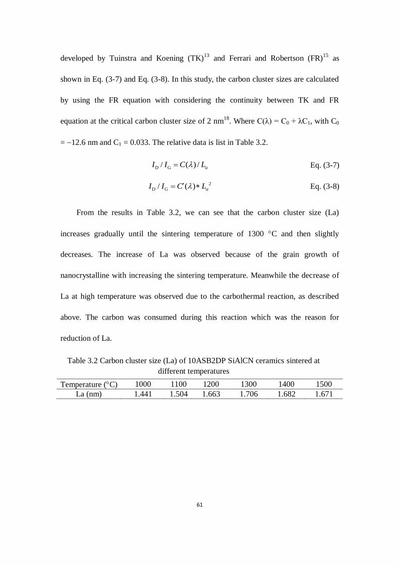
61
developed by Tuinstra and Koening (TK)13
and Ferrari and Robertson (FR)15
as
shown in Eq. (3-7) and Eq. (3-8). In this study, the carbon cluster sizes are calculated
by using the FR equation with considering the continuity between TK and FR
equation at the critical carbon cluster size of 2 nm18
. Where C(λ) = C0 + λC1, with C0
= 12.6 nm and C1 = 0.033. The relative data is list in Table 3.2.
D G/ ( ) / aI I C L Eq. (3-7)
2
D G/ ( ) aI I C L Eq. (3-8)
From the results in Table 3.2, we can see that the carbon cluster size (La)
increases gradually until the sintering temperature of 1300 C and then slightly
decreases. The increase of La was observed because of the grain growth of
nanocrystalline with increasing the sintering temperature. Meanwhile the decrease of
La at high temperature was observed due to the carbothermal reaction, as described
above. The carbon was consumed during this reaction which was the reason for
reduction of La.
Table 3.2 Carbon cluster size (La) of 10ASB2DP SiAlCN ceramics sintered at
different temperatures
Temperature (C) 1000 1100 1200 1300 1400 1500
La (nm) 1.441 1.504 1.663 1.706 1.682 1.671

62
References:
1. Trassl, S., et al., Structural characterisation of silicon carbonitride ceramics
derived from polymeric precursors. Journal of the European Ceramic Society,
2000. 20(2): p. 215-225.
2. Seitz, J., et al., Structural investigations of Si/C/N-ceramics from polysilazane
precursors by nuclear magnetic resonance. Journal of the European Ceramic
Society, 1996. 16(8): p. 885-891.
3. Dhamne, A., et al., Polymer-ceramic conversion of liquid
polyaluminasilazanes for SiAlCN ceramics. Journal of the American Ceramic
Society, 2005. 88(9): p. 2415-2419.
4. Li, Y.L., et al., Thermal cross-linking and pyrolytic conversion of
poly(ureamethylvinyl)silazanes to silicon-based ceramics. Applied
Organometallic Chemistry, 2001. 15(10): p. 820-832.
5. Brodie, N., J.P. Majoral, and J.P. Disson, An Nmr-Study of the Step-by-Step
Pyrolysis of a Polysilazane Precursor of Silicon-Nitride. Inorganic Chemistry,
1993. 32(21): p. 4646-4649.
6. Sarkar, S., et al., Structural Evolution of Polymer-Derived Amorphous SiBCN
Ceramics at High Temperature. Journal of Physical Chemistry C, 2011.
115(50): p. 24993-25000.
7. Chen, Y., et al., Self-assembled carbon-silicon carbonitride nanocomposites:
highperformance anode materials for lithium-ion batteries. Journal of
Materials Chemistry, 2011. 21(45): p. 18186-18190.

63
8. Seyferth, D., G. Brodt, and B. Boury, Polymeric aluminasilazane precursors
for aluminosilicon nitride. Journal of Materials Science Letters, 1996. 15(4): p.
348-349.
9. Boury, B. and D. Seyferth, Preparation of Si/C/Al/N ceramics by pyrolysis of
polyaluminasilazanes. Applied Organometallic Chemistry, 1999. 13(6): p.
431-440.
10. Berger, F., et al., Solid-state NMR studies of the preparation of Si-Al-C-N
ceramics from aluminum-modified polysilazanes and polysilylcarbodiimides.
Chemistry of Materials, 2004. 16(5): p. 919-929.
11. Wang, Y.S., et al., Effect of Thermal Initiator Concentration on the Electrical
Behavior of Polymer-Derived Amorphous Silicon Carbonitrides. Journal of
the American Ceramic Society, 2008. 91(12): p. 3971-3975.
12. Trassl, S., et al., Electrical properties of amorphous SiCxNyHz-ceramics
derived from polyvinylsilazane. Journal of the European Ceramic Society,
2003. 23(5): p. 781-789.
13. Tuinstra, F. and J.L. Koenig, Raman Spectrum of Graphite. Journal of
Chemical Physics, 1970. 53(3): p. 1126-&.
14. Sadezky, A., et al., Raman micro spectroscopy of soot and related
carbonaceous materials: Spectral analysis and structural information. Carbon,
2005. 43(8): p. 1731-1742.
64
15. Ferrari, A.C. and J. Robertson, Interpretation of Raman spectra of disordered
and amorphous carbon. Physical Review B, 2000. 61(20): p. 14095-14107.
16. Ferrari, A.C. and J. Robertson, Resonant Raman spectroscopy of disordered,
amorphous, and diamondlike carbon. Physical Review B, 2001. 64(7).
17. Ferreira, E.H.M., et al., Evolution of the Raman spectra from single-, few-,
and many-layer graphene with increasing disorder. Physical Review B, 2010.
82(12).
18. Zickler, G.A., et al., A reconsideration of the relationship between the
crystallite size L-a of carbons determined by X-ray diffraction and Raman
spectroscopy. Carbon, 2006. 44(15): p. 3239-3246.

65
CHAPTER FOUR: ELECTRIC AND DIELECTRIC PROPERTIES
OF SiAlCN CERAMICS
The electric properties are considered one of the most important properties of
PDCs because they reveal a better and deeper understanding of the intrinsic science of
PDC. Previous studies indicate the semiconductor behavior can be sustained to very
high temperatures (such as ~1300 C), which is much higher than that of any existing
ceramics (< 800 C). This unique property makes the PDCs good candidates for high
temperature applications. The electric properties of different PDCs systems are
reported, such as SiCN, SiOCN and SiBCN, but there are virtually no publications
about the electric properties of SiAlCN. The dielectric property is another important
function widely used for sensing applications. The dielectric property studies of PDC
are very limited and there are no open reports about the dielectric property of SiAlCN
ceramics to the best of the author’s knowledge.
In this chapter, the electric and dielectric properties of SiAlCN ceramics were
characterized and the possible mechanisms were discussed. It was observed that both
the conductivity and dielectric constant increased dramatically with increasing
temperature (both sintered and test temperature), which indicates that SiAlCN
ceramics are well suited for high temperature sensor applications. The “electric field
concentration” model was proposed and this model is consistent with the
experimental data. The temperature dependent conductivity shows that the conducting
mechanism of SiAlCN ceramics follows the Arrhenius equation. The huge dielectric

66
constant is caused by the space charge effect, which was confirmed by the
impendence analysis and the high loss observed from the SiAlCN ceramics exposed
to high temperature (both sintered and test temperature), were caused by the
increasing of conductivity of the materials.
4.1 Experimental procedure
The cylinder SiAlCN ceramics samples, as received and obtained using the
procedure described in Chapter 3, were further heat treated at 800 °C for 2 hours in air
to remove the carbon deposited on to the surface during pyrolysis. Then, the two
surfaces of the SiAlCN ceramics were polished by 15, 9 and 6 m diamond plate
respectively. The polished samples were cleaned by ultrasonic for 5 min in acetone
and dried at 120 C for 1 hour. Finally, the conducting silver paste (SPI) was applied
on both sides as the electrode. The D.C. conductivities were calculated from the I-V
curves achieved by KEITHLEY 2400. The dielectric properties were characterized by
using the Agilent 4298A with the frequency of 20-2 MHz.

67
4.2 Results and discussion
4.2.1 Electric properties of SiAlCN ceramics
Figure 4.1 I-V curves and the curve fitting of SiAlCN ceramics sintered at different
temperature (a) 1000 C, (b) 1100 C, (c) 1200 C, (d) 1300 C, (e) 1400 C.
The D.C. conductivity of SiAlCN ceramic samples were calculated by knowing
the slop of I-V curve. Figure 4.1 (a)-(e) show the I-V curves and curve fitting results
with 10ASB2DP SiAlCN ceramic samples sintered at various temperatures of 1000,

68
1100, 1200, 1300, and 1400 C, respectively. From the results in Figure 4.1, we can
see that the I-V curves are all in perfect linear relation indicating SiAlCN ceramics
follow the Ohm’s law. The conductivities of SiAlCN ceramics sintered at various
temperatures are listed in Table 4.1 and plotted in Figure 4.2, and the relative data of
SiCN are shown and plotted too for comparison.
Table 4.1 Conductivities of SiAlCN and SiCN sintered at various temperatures.
Activation
energy (eV)
SiAlCN
Temperature (C)
1000 1100 1200 1300 1400
5.1 Conductivity
(Ohm*cm)1
4.14E10 1.16E09 1.33E08 2.03E07 3.31E06
SiCN*
Temperature (C)
1000 1100 1200 1300 1350
3.41 Conductivity
(Ohm*cm)1
2.06E09 1.46E08 1.21E07 7.69E07 1.50E06
*: Yaohan Chen “STRUCTURE AND PROPERTIES OF POLYMER-
DERIVED SiBCN CERAMICS” University of Central Florida, PhD dissertation
(2012).
1000 1100 1200 1300 1400
0.0
5.0x10⁻⁷
1.0x10⁻⁶
1.5x10⁻⁶
2.0x10⁻⁶
2.5x10⁻⁶
3.0x10⁻⁶
3.5x10⁻⁶
Temperature (C)
Co
nd
ucti
vit
y (
Oh
mc
m)
1
SiAlCN
SiCN *
Figure 4.2 Conductivity of SiAlCN ceramics sintered at different temperatures.

69
The results in Table 4.1 and Figure 4.2 reveal that the conductivity of SiAlCN
increases with increasing pyrolysis temperature and the difference is about four orders
of magnitude. The observation begs the question; why does the conductivity increase
with increasing the pyrolysis temperature dramatically? In order to answer this
question, let’s take a look at the basic structure of the PDCs. There are mainly two
components of the PDC one is amorphous matrix SiCxN1-x (0<x< 4), the other is free
carbon and the former one is low conductive matrix and the later one is high
conductive phase. This structure is similar with the composite with a low conductivity
matrix and a high conductivity dispersed particles, first reported by Maxiwell1. Most
recently, L. Woo and co-works found that the conductivity was improved greatly in
the CNT/cement system by the strong field concentration2. We believe that in our
system the conductivity increase is related to the field concentration. Therefore, we
propose the electric field concentration between the conductive free carbon clusters
occurs in our SiAlCN system, as illustrated in Figure4.3.
Figure4.3 Schematic illustration of electric field concentration in SiAlCN system.

70
As can be seen in Figure4.3, the charge carriers (electrons and holes) in the high
conductive free carbon clusters will separate to each other and move to the positive
and negative electrode, respectively, when the external electric field is applied. The
separation of electrons and holes will cause a strong electric field concentration in
between two free carbon clusters and hereby the apparent conductivity increased in
the overall material. Since the effective electric field is much higher than the external
electric field, due to the high electric field concentration, but the electric field used for
conductivity calculation is still the external one but not the effective one. As a result,
the conductivity is higher than that should be. Meanwhile, the electric field
concentration will be enhanced if the conductivity of free carbon increased, for the
higher conductivity, the more movable charge carriers. These results are consistent
with the structure analysis results described in Chapter 2. In Chapter 2, the Raman
spectra shows an up-shift of G-peak position, narrow of the FWHM and EPR spectra
shows an reducing of defect concentration with increasing the sintered temperature.
These are all the signs of the free carbon becoming order and order with increasing
the sintered temperature. The conductivity of free carbon will increase when the free
carbon becomes order and order for the increasing of sp2/sp
3 ratio. In other words, the
higher sintered temperature, the higher conductivity of free carbon and therefore, the
stronger of the electric field concentration.
Furthermore, if the proposed model is correct, the following facts will be true:
there should be only one conducting mechanism before the electric field concentration

71
was established or when the electric field concentration was neglected; and there
should be two conducting mechanisms when the electric field concentration was
established. In order to found out the truth, complex impedance of SiAlCN ceramic is
investigated, as shown in Figure 4.4. It found that there is only one arc for SiAlCN
ceramics sintered at 1000 and 1200 C, and two semicircles for the sample sintered at
1400 C. It means that there is only one impedance mechanism for the samples
sintered at low temperature (1000 and 1200 C) and two impedance mechanisms for
the high temperature one (1400 C). For the samples sintered at low temperature
(1000 and 1200 C), the free carbon are not conductive enough (for it is not order
enough) to effect the overall impendence, so the material is similar to a single phase
material and shows a matrix only conducting mechanism. For the sample sintered at
high temperature (1400 C), the free carbon are highly ordered with a high
conductivity and contribute the overall impedance, so the material shows two
conducting mechanism (matrix + free carbon in series). The complex impendence
results approve that the proposed “electric field concentration” is a right model for the
conducting mechanism of our material system.

72
0.0 5.0x10⁷
1.0x10⁸
1.5x10⁸
0.0
5.0x10⁷
1.0x10⁸
1.5x10⁸
2.0x10⁸
2.5x10⁸
3.0x10⁸
Z'' (
)
Z' ()
1000
0 1x10⁷
2x10⁷
3x10⁷
4x10⁷
0.0
4.0x10⁶
8.0x10⁶
1.2x10⁷
1.6x10⁷
Z'' (
)
Z' ()
1200
0.0 5.0x10⁴
1.0x10⁵
1.5x10⁵
0.0
2.0x10⁴
4.0x10⁴
6.0x10⁴
Z'' (
)
Z' ()
1400
Figure 4.4 Complex impedance analysis of SiAlCN ceramic sintered at different
temperatures (a) 1000 C, (b) 1200 C and (c) 1400 C.
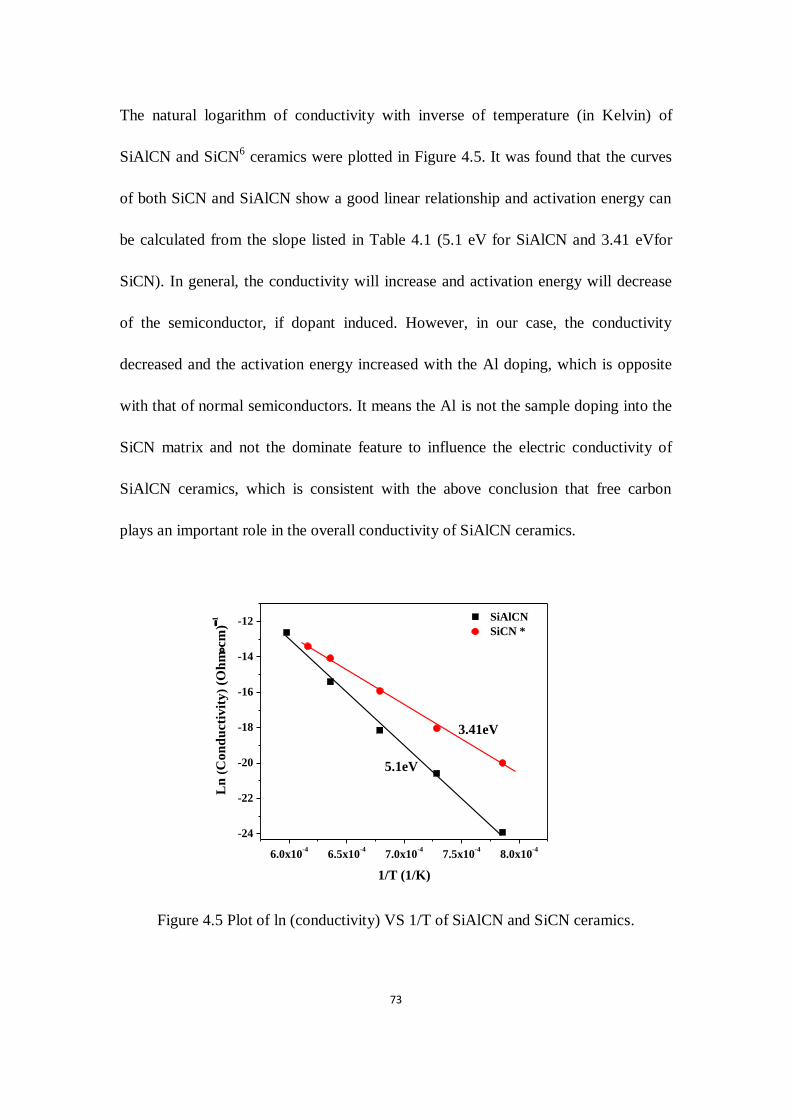
73
The natural logarithm of conductivity with inverse of temperature (in Kelvin) of
SiAlCN and SiCN6 ceramics were plotted in Figure 4.5. It was found that the curves
of both SiCN and SiAlCN show a good linear relationship and activation energy can
be calculated from the slope listed in Table 4.1 (5.1 eV for SiAlCN and 3.41 eVfor
SiCN). In general, the conductivity will increase and activation energy will decrease
of the semiconductor, if dopant induced. However, in our case, the conductivity
decreased and the activation energy increased with the Al doping, which is opposite
with that of normal semiconductors. It means the Al is not the sample doping into the
SiCN matrix and not the dominate feature to influence the electric conductivity of
SiAlCN ceramics, which is consistent with the above conclusion that free carbon
plays an important role in the overall conductivity of SiAlCN ceramics.
6.0x10⁻⁴
6.5x10⁻⁴
7.0x10⁻⁴
7.5x10⁻⁴
8.0x10⁻⁴
-24
-22
-20
-18
-16
-14
-12
3.41eV
SiAlCN
SiCN *
Ln(
Co
nd
ucti
vit
y)
(Oh
mc
m)
1
1/T (1/K)
5.1eV
Figure 4.5 Plot of ln (conductivity) VS 1/T of SiAlCN and SiCN ceramics.

74
As discussed above, the conductivity of free carbon affects the overall
conductivity of SiAlCN significantly. At the same time, the conductivity of SiAlCN is
highly related to the degree of crystallization of free carbon. Jiang and colleges
reported that the activity energy was 7.9 eV for “oxygen rich” SiCN system7. The
SiAlCN system in our research has a medium of oxygen (observed from the 29
Si
solid-state NMR results, oxygen is present in SiAlCN ceramics by form of “SiO4”
units) with the activation energy of 5.1 eV and the activation energy of “oxygen free”
SiCN system was 3.41eV reported by Chen and co-works. We believe that the
presence of oxygen restricts the crystallization (or sp3-sp
2 transition) of free carbon
and, thereby, increases the activation energy. The bonds between C and O were
revealed XPS technique shown in Figure 4.6. The C-O-C or O-C (O)-O bands were
observed by the superfine structure analysis of carbon XPS, which indicated that the
oxygen does have some effect on the free carbon. Unfortunately, how the oxygen
effects the conductivity of free carbon is still unknown further investigation is
requieed.
Figure 4.6 XPS results of SiAlCN ceramics sintered at 1000 C.

75
The temperature dependence electric conductivity of 10ASB2DP SiAlCN
ceramic sintered at 1000 C was tested within the temperature range starting at room
temperature to 500 C. The high temperature conductivity characterization was
carried out at the muffle furnace without any protect atmosphere and the silver paste
as electrode.
Figure 4.7 shows the temperature dependent conductivity of 10ASB2DP sintered
at 1000 C SiAlCN ceramic with the test temperature up 500 C (limited by the stable
using temperature of silver electrode). As can be seen in Figure 4.7 the electric
conductivity increases continually with increasing temperature. A significant increase,
three orders of magnitude, was found from room temperature to 500 C. This strong
temperature dependence resistivity behavior suggests that the SiAlCN materials are
promising for use as high temperature sensor.
0 100 200 300 400 500
0.0
1.0x10⁻⁶
2.0x10⁻⁶
3.0x10⁻⁶
Temperature (C)
Co
nd
ucti
vit
y (
Oh
mc
m)
1
10ASB2DP-1000C
Figure 4.7 Temperature dependent conductivity of SiAlCN and SiCN ceramics.

76
There are mainly two possible conducting mechanisms: one is the
semiconducting band-gap model which follows Arrhenius equation as shown in Eq.
(4-1), and the other is called variable range hopping (VRH), which follows Mott’s
equation as shown in Eq. (4-2).
0 expE
kT
Eq. (4-1)
14
00 exp
T
T
Eq. (4-2)
Where is conductivity, is a pre-exponential factor, is the activation
energy, the gap between the Fermi level and the energy state which the charge carriers
are excited, and k is the Boltzmann constant. is given by:
3
0
18.1
( )F
TkN E
Where α is inverse of the localization length of the wave function for the excited
electron, is the density of the localized states around Fermi level.
In the semiconducting band-gap model, the conductivity is controlled primarily
by the concentration of the mobile charge carriers which is a highly temperature
dependent processing and determined by the activation energy. In contrast, for the
VRH model, the charge carriers will jump back and forth one unoccupied state to
another near the Fermi level; conductivity is determined by both hopping distance and
activation energy.

77
The parameter
determines the type of conducting mechanisms and thus, it
follows that the parameter is very importants. If , then the electric
conductivity is controlled by the semiconducting band-gap model, follows the
Arrhenius equation; if the the electric conductivity is followed the Mott’s
law.
The natural logarithm of conductivity with inverse of test temperatures (in
Kelvin) was plotted in Figure 4.8 and the relative activation energies were calculated
by curve fitting. It was found that the Arrhenius fit can be accommodated by two
different activation energies of 0.57 eV and 0.23 eV for high and low temperature
sections, respectively. Considering the values of KT in the testing temperature range,
are 0.0026 eV at room temperature and 0.066 eV at 500 C. Since, is
satisfied then it follows that the semiconducting band-gap conducting mechanism.
1.0x10⁻³
1.5x10⁻³
2.0x10⁻³
2.5x10⁻³
3.0x10⁻³
3.5x10⁻³
-20
-18
-16
-14
-12
-10
0.57eV
10ASB2DP-1000C
ln (
co
nd
ucti
vit
y)
(Oh
mc
m)
1
1/T (1/K)
0.23eV
Figure 4.8 Plot of ln (conductivity) VS 1/T of SiAlCN at different test temperatures.
78
4.2.2 Dielectric properties of SiAlCN ceramics
Both the dielectric constant and loss were characterized for SiAlCN ceramics
sintered at various temperatures (1000, 1100, 1200, 1300 and 1400 C) using the
Agilent E4980A within the frequency range between 20 Hz to 2 MHz. The dielectric
constant and loss were calculated by the following equations.
**
0
C d
A
Eq. (4-3)
tan
Eq. (4-4)
Where are the complex dielectric constant and capacitance,
respectively. is the dielectric constant of free space; A and d are the electrode area
and sample thickness. δ is dielectric loss, and are the image and real part of
dielectric constant, respectively.
The results were plotted in Figure 4.9 and Figure 4.10, respectively. The
dielectric constant and loss for SiAlCN ceramics sintered at different temperatures at
specific frequencies (1, 10, 100 kHz and 1 MHz) were listed in Table 4.2 and plotted
in Figure 4.11 and Figure 4.12. It was found that the dielectric constant and loss
decreased with increasing frequency. The dielectric constant was higher at low
frequency than that of high frequency because of the polarizations get enough time to
response with the electric field at low frequencies; in contrast, the electric field at high
frequencies allow only part of the polarizations to catch up with it, so the dielectric
constant is smaller at high frequencies. The dielectric loss is caused by the energy
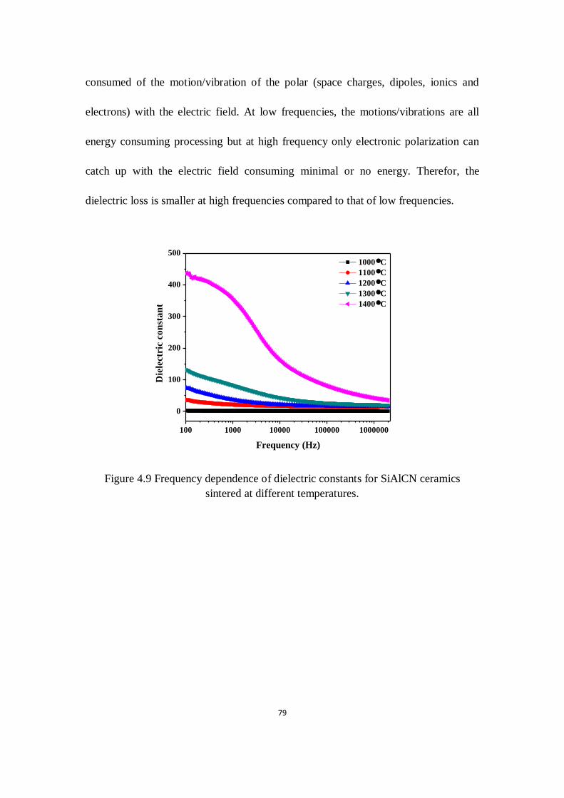
79
consumed of the motion/vibration of the polar (space charges, dipoles, ionics and
electrons) with the electric field. At low frequencies, the motions/vibrations are all
energy consuming processing but at high frequency only electronic polarization can
catch up with the electric field consuming minimal or no energy. Therefor, the
dielectric loss is smaller at high frequencies compared to that of low frequencies.
100 1000 10000 100000 1000000
0
100
200
300
400
500
Die
lectr
ic c
on
sta
nt
Frequency (Hz)
1000 C
1100 C
1200 C
1300 C
1400 C
Figure 4.9 Frequency dependence of dielectric constants for SiAlCN ceramics
sintered at different temperatures.

80
100 1000 10000 100000 1000000
0
20
40
60
80
100 1000 C
1100 C
1200 C
1300 C
1400 C
Die
lectr
ic l
oss
Frequency (Hz)
Figure 4.10 Frequency dependence of dielectric loss of SiAlCN ceramics sintered at
different temperatures.
Table 4.2 Dielectric constants and loss of SiAlCN ceramics at different sintered
temperatures and frequencies.
T(oC) Dielectric constant Dielectric loss
1kHz 10kHz 100kHz 1MHz 1kHz 10kHz 100kHz 1MHz
1000 1.85 1.58 1.48 1.43 0.25 0.09 0.03 0.01
1100 21.55 17.46 16.06 15.53 0.37 0.12 0.04 0.02
1200 36.99 21.60 17.26 15.68 1.12 0.39 0.13 0.05
1300 82.93 43.23 26.40 20.95 4.44 1.20 0.39 0.14
1400 356.73 161.91 79.66 41.98 11.63 2.62 0.60 0.19

81
1K 10K 100K 1M0
50
100
150
200
250
300
350
Frequency (Hz)
Die
lectr
ic c
on
sta
nt
1000
1100
1200
1300
1400
Figure 4.11 Dielectric constants of SiAlCN ceramics at specific frequency and various
sintered temperatures.
1K 10K 100K 1M0
3
6
9
12
Die
lectr
ic l
oss
Frequency (Hz)
1000
1100
1200
1300
1400
Figure 4.12 Dielectric loss of SiAlCN ceramics at specific frequency and various
sintered temperatures.
As can be seen, the dielectric constant of SiAlCN ceramics sintered at 1400 C is
more than 300 times higher than that of the samples sintered at 1000 C, which is a
huge improvement. We believe that this huge improvement is due to the space charge

82
effect. The space charge is formed at the interface between the SiCN matrix and free
carbon, as illustrated in Figure 4.13. The charge carriers disperse uniformly when
there is no electric field (Figure 4.13 (a)). In contrast, the charge carriers separate and
accumulate at the interface (Figure 4.13 (b)) when the external electric field is applied,
the space charge is set up. The formed space charge established an inner electric field,
opposite in direction to the external one and causing a dramatic increase in the
dielectric constant. It is easy to understand that the more trapped charge carriers the
larger of inner electric field and the higher dielectric constant can be observed. The
trapped charge carriers within the samples sintered at 1400 C were higher than that
of the samples sintered at 1000. This means that the space charge effect will be
stronger for 1400 C samples than that of the samples sintered at1000 C. This is the
reason the dielectric constant of SiAlCN samples sintered at 1400 C is observed to
be much higher than that of 1000 C samples at low frequencies.
Figure 4.13 Schematic illustration of established space charge within SiAlCN system
(a) without electric field (b) with electric field
As can be seen, the dielectric loss increases dramatically with increasing sintered
temperature. This observation begs the question; does the dielectric loss truly cause

83
by the polarization? In order to determine the answer, the relationship between the
conductivity and image part of the dielectric constant must be considered, as shown in
Eq. (4-5).
0
Eq. (4-5)
If we apply the logarithm on both sides of Eq. (4-5), we obtain in Eq. (4-6)
0 0
log log log log2 2
ff
Eq. (4-6)
Where is conductivity, f is frequency.
The logarithm of the imaginary part of the dielectric constant and the logarithm
of the frequency should be linearly with a slope of 1, if the conducting behavior
dominates to the imaginary part of dielectric constant. The results are plotted in
Figure 4.14 and the linear fit results are shown in Figure 4.15. The slopes of the curve
fitting results are listed in Table 4.3. The slopes increase from 0.56 to 1 gradually with
sintering temperature range between 1000 C and 1400 C, indicating that with
increasing sintered temperature the conducting behavior becomes more dominate,
resulting in high dielectric loss. The results agree with the D.C. conductivity of
SiAlCN ceramics very well (the D.C. conductivity increase with increasing the
sintered temperature.)

84
100 1000 10000 100000 1000000
0.01
0.1
1
10
100
1000
10000
1000
1100
1200
1300
1400'
'
Frequency (Hz)
Figure 4.14 Dielectric loss of SiAlCN ceramics at specific frequencies and different
sintered temperatures.

85
Figure 4.15 Dielectric loss of SiAlCN ceramics at specific frequency and different
sintered temperatures.
Table 4.3 Slops of the linear fit of logarithm of the imaginary part of the dielectric
constant and the logarithm of frequency of 10ASB2DP-SiAlCN ceramics.
T(C) 1000 1100 1200 1300 1400
Slop 0.56 0.66 0.78 0.96 0.99
The temperature dependent dielectric constants and loss were measured by using
the Agilent 4298A and a muffle furnace for heat up the samples. The frequency and

86
temperature range were 20 Hz - 2 MHz and room temperature to 450 C, respectively.
The temperature dependent dielectric constant and loss are shown in Figure 4.16 and
Figure 4.17. It was found that the dielectric constant and loss both increased with
increasing test temperature. The dielectric constant and loss became larger at low
frequencies than that of at high frequencies, similar to the frequency dependent
properties discussed above. The most polar (ions, atoms and electrons) will gain
energy when the temperature increases, which in turn makes them in a high energy
state (which means they are easier to move than that in the equilibrium state). These
polar with higher energy cause higher polarization, therefore, the dielectric constant
and loss increase with increasing temperature. The number of trapped charge carriers
increase with increasing temperature, and the strong space charge effect could be
observed when there are enough trapped charge carriers present. The impendence
analysis of SiAlCN ceramics, tested at different temperature, reveal that the strong
space charge effect were observed at the temperature around 400 C, illustrated in
Figure4.18. There was only one arc or semicircle (Figure4.18 (a) and (b)) before 400
C and there was a small tail for the sample tested at 400 C caused by the space
charge effect.
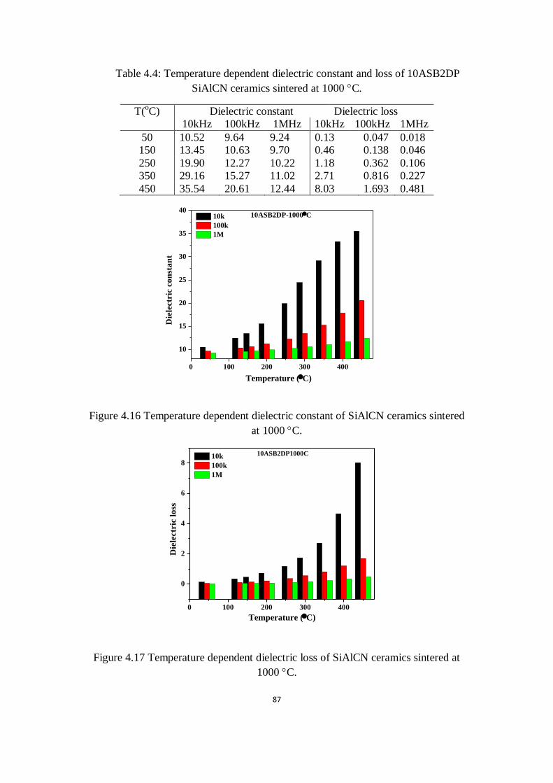
87
Table 4.4: Temperature dependent dielectric constant and loss of 10ASB2DP
SiAlCN ceramics sintered at 1000 C.
T(oC) Dielectric constant Dielectric loss
10kHz 100kHz 1MHz 10kHz 100kHz 1MHz
50 10.52 9.64 9.24 0.13 0.047 0.018
150 13.45 10.63 9.70 0.46 0.138 0.046
250 19.90 12.27 10.22 1.18 0.362 0.106
350 29.16 15.27 11.02 2.71 0.816 0.227
450 35.54 20.61 12.44 8.03 1.693 0.481
0 100 200 300 400
10
15
20
25
30
35
4010ASB2DP-1000C
Die
lectr
ic c
on
sta
nt
Temperature (C)
10k
100k
1M
Figure 4.16 Temperature dependent dielectric constant of SiAlCN ceramics sintered
at 1000 C.
0 100 200 300 400
0
2
4
6
8
10ASB2DP1000C
Die
lectr
ic l
oss
Temperature (C)
10k
100k
1M
Figure 4.17 Temperature dependent dielectric loss of SiAlCN ceramics sintered at
1000 C.

88
0.0 5.0x10⁶
1.0x10⁷
1.5x10⁷
2.0x10⁷
2.5x10⁷
0.0
2.0x10⁶
4.0x10⁶
6.0x10⁶
8.0x10⁶ 200
Z'' (
)
Z' ()
0 1x10⁶
2x10⁶
3x10⁶
4x10⁶
2.0x10⁵
4.0x10⁵
6.0x10⁵
8.0x10⁵
1.0x10⁶
1.2x10⁶
300
Z'' (
)
Z' ()
0.0 2.0x10⁵
4.0x10⁵
6.0x10⁵
8.0x10⁵
1.0x10⁶
5.0x10⁴
1.0x10⁵
1.5x10⁵
2.0x10⁵
2.5x10⁵
3.0x10⁵
400
Z'' (
)
Z' ()
Figure 4.18 Complex impendence analysis of SiAlCN ceramics at different tested
temperatures (a) 200 oC (b) 300
oC (c) 400
oC.

89
References:
1. J.C. Maxwell, A Treatise on Electricity and Magnetism, 2nd
edn, Vol. 1, p435,
Clarendon Press, Oxford.
2. L. Woo, S. Wansom, A.D. Hixson, M.A. Campo, and T.O. Mason, A universal
equialent circuit model for the impedance response of composites, J. Mater. Sci.,
38, 2265-2270, (2003).
3. A. C. Ferrari, S. E. Rodil, J. Robertson and W. I. Milne, "Is stress necessary to
stabilise sp3 bonding in diamond-like carbon?" Diam. Relat. Mater., 11 [3–6],
994-999 (2002).
4. A. C. Ferrari, B. Kleinsorge, N. A. Morrison, A. Hart, V. Stolojan and J.
Robertson, "Stress reduction and bond stability during thermal annealing of
tetrahedral amorphous carbon," J. Appl. Phys., 85 [10], 7191-7197 (1999).
5. D. S. Grierson, A. V. Sumant, A. R. Konicek, T. A. Friedmann, J. P. Sullivan, and
R. W. Carpick, “Thermal stability and rehybridization of carbon bonding in
tetrahedral amorphous carbon,” J. Appl. Phys. 107, 033523 (2010).
6. Yaohan Chen “STRUCTURE AND PROPERTIES OF POLYMER-DERIVED
SiBCN CERAMICS”’ University of Central Florida, PhD dissertation, (2012).
7. Tao Jiang “ELECTRONIC PROPERTIES AND MICROSTRUCTURES OF
AMORPHOUS SiCN CERAMICS DERIVED FROM POLYMER
PRECURSORS” University of Central Florida, PhD dissertation, (2009).
90
CHAPER FIVE: HIGH TEMPERATURE SENSOR
FABRICATION AND CHARACTERIZATION
Temperature has to be monitored to prevent damage of devices and improve
performance in high temperature and harsh environments in many applications, for
example, gas turbines, nuclear reactors, high speed vehicles and automotives.
However, fabrication of such sensors faces a huge technical challenge. The major
hurdle is that the sensors must survive harsh environments, including high
temperatures, high stress, corrosive species and/or radiation. In addition, the sensor
materials must maintain specific properties at high temperatures in order to provide
means for sensing; they must do so in an easy-to-microfabricate manner in order to
lower costs. These requirements basically prevent the use of most available sensors1-7
.
Recently, polymer-derived ceramics (PDCs) have been considered suitable materials
for making high-temperature microelectromechanical systems (MEMS)/micro-
sensors8. Previous studies revealed that PDCs, synthesized from the thermal
decomposition of polymeric precursors, exhibit excellent thermomechanical
properties, such as high thermal stability9,10
, high oxidation/corrosion resistance11-15
and high temperature multifunctionalities16,17
.
This chapter will discuss the high temperature sensor fabrication, Whetstone
bridge circuit design and sensor test by using the SiAlCN ceramics basing on their
temperature dependence resistance properties.

91
5.1 Polymer derived SiAlCN sensor fabrication
The fabrication procedure of polymer derived temperature sensor is
demonstrated by using the 10ASB2DP-1000C SiAlCN sample. The micro-
machining technique is for sensor and the basic procedures are shown in Figure 5.1
and illustrated as following:
(1) A hydraulic laboratory press (Automatic 4533, Carver, Inc., Wabash, IN) was
used to crosslinked SiAlCN precursor (infusible polymer) to a disk shape (green
body) with the dimension of Φ12.5mm in diameter and 4~6 mm in thickness. The
green body was heat treated at 200 C for 24 hours in the oven.
(2) A precision CNC dicing/cutting diamond saw (SYJ-400, Richmond, CA) was
used to cut a rectangular SiAlCN sensor head (polymer state) from the green body
mentioned in step (1).
(3) Two holes were drilled on top of the sensor head achieved in step (2) with the
diameter of ~350 m and ~1.5 mm in depth by applying the micro machining
technique.
(4) Liquid SiAlCN precursor was infiltrated into the two holes under a vacuum.
(5) Pt wires were fed into the manufactured holes and crosslinked at 80 C for 24
hours in order to to hold the Pt wires.
(6) The as-received sensor head with Pt wires was pyrolyzed at 1000 C for 4 hours to
obtain a SiAlCN ceramic sensor (with Pt wires). The Overall size of the
assembled sensor is 3.4mm2.7mm1.2mm, shown in Figure 5.1 (b)

92
Figure 5.1 (a) SiAlCN ceramic sensor fabrication procedure and (b) optical image of
sensor.
There are two key factors that should be mentioned here. First and foremost, the
heat treatment process of the green body is required to make it strong enough to
sustain micro-machining. Secondly, the size of the hole for the Pt wire needed to be
selected carefully; this is due to the natural shrinkage (~22%) of the SiAlCN ceramics
during the pyrolysis and inversely. Inversely, the Pt wire will expand at the same time
so optimal parameters concerning the hole size must be determined. If the precursor
layer in between the Pt wire and sensor head is too thin (the case of small hole), there
will not be enough bonding force to hold the Pt wire; as a result the Pt wire will fall
off (extreme situation: no precursor layer). If the precursor layer is too thick (the case
of big hole), the ceramic sensor will be broken by the tension stress from the
expansion of the Pt wire (extreme situation: Pt wire sounded by precursor only).
Therefore, the thickness of the precursor (or the size of the hole) should be carefully
selected in order to get a good bonding but not break the ceramic sensor. In this case
(a)
(b)

93
the hole, with diameter of ~350 m was proved to be sufficient. Figure 5.2 shows the
SEM images of the Pt wire bonding of SiAlCN sensor. As we can see in Figure 5.2 (a)
the sensor head cracked due to the tension force from Pt wire and Figure 5.2 (b)
indicated a very good bonding between the Pt wire and ceramic sensor head.
Figure 5.2 SEM images of Pt wire bonding of the ceramic sensor head.
5.2 Wheatstone bridge circuit design and analysis
A Wheatstone bridge is an electrical circuit used to measure an
unknown electrical resistance by balancing two legs of a bridge circuit, one leg of
which includes the unknown component; invented by Samuel Hunter Christie in 1833
and improved and popularized by Sir Charles Wheatstone in 1843. The principle of
the circuit is that if three out of four resistances are known, and current in the cross
branch is zero, the fourth resistance could be determined. This experimental setup, the
Wheatstone circuit shown in Figure 5.3, was applied for the temperature sensor
measurement. Where R1, R2 and R3 are standard resistors and Rx is the SiAlCN
ceramic sensor.
Pt wire
SiAlCN
sensor head
(a) (b)
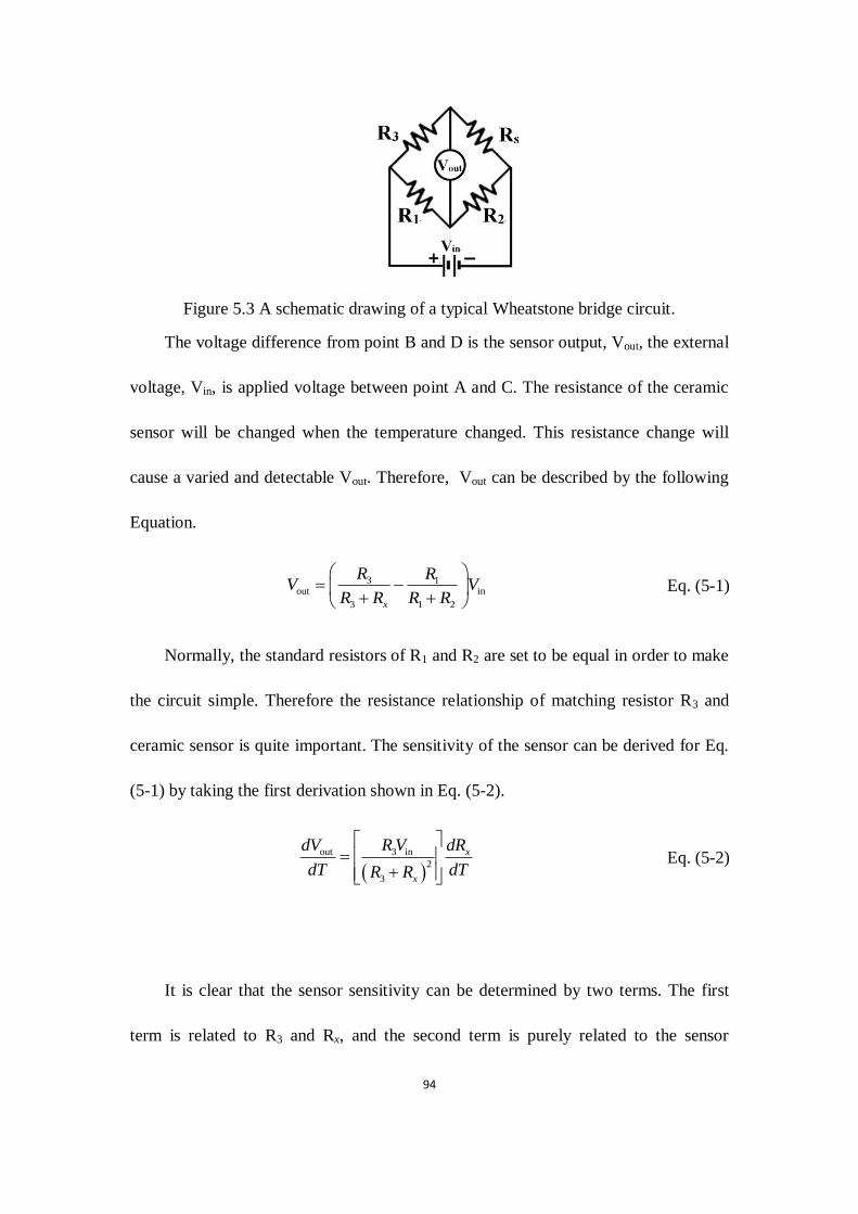
94
Figure 5.3 A schematic drawing of a typical Wheatstone bridge circuit.
The voltage difference from point B and D is the sensor output, Vout, the external
voltage, Vin, is applied voltage between point A and C. The resistance of the ceramic
sensor will be changed when the temperature changed. This resistance change will
cause a varied and detectable Vout. Therefore, Vout can be described by the following
Equation.
3 1out in
3 1 2x
R RV V
R R R R
Eq. (5-1)
Normally, the standard resistors of R1 and R2 are set to be equal in order to make
the circuit simple. Therefore the resistance relationship of matching resistor R3 and
ceramic sensor is quite important. The sensitivity of the sensor can be derived for Eq.
(5-1) by taking the first derivation shown in Eq. (5-2).
out 3 in
2
3
x
x
dV R V dR
dT dTR R
Eq. (5-2)
It is clear that the sensor sensitivity can be determined by two terms. The first
term is related to R3 and Rx, and the second term is purely related to the sensor

95
property of temperature dependent resistivity. In order to get good sensitivity, these
two parts must to be considered. First, the second part of Eq. (5-2) will be discussed.
100 200 300 400 500 600 700
0
2000
4000
6000
300 400 500 600
0
50
100
150
200
250
300 Sensor resistance
Re
sis
tan
ce
(M
)
Temperature (oC)
Sensor resistanceR
esi
sta
nce (
M
)
Temperature (C)
Figure 5.4 The sensor resistance changes with temperature (the imbedded plot shows
the high temperature range).
The sensor resistance changes with temperature depicted in Figure 5.4. It was
found that sensor resistance, in a fairly large range from 4592 MΩ to 4.42 MΩ,
continues to decrease as temperature change from room temperature to 600 C. Based
on the previous results, the conducting mechanism is semiconducting band-gap model,
which follows Arrhenius equation, shown in Eq. (5-3). Combining with Ohm’s law
(
) and applying the natural logarithm, allows us to obtain Eq. (5-4);
indicating that ln(1/R) VS (T 1
) should have a linear relationship and the result is
plotted in Figure 5.5.
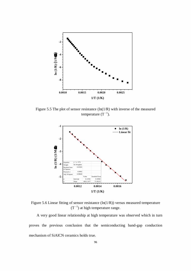
96
0.0010 0.0015 0.0020 0.0025
-8
-6
-4
-2
ln (
1/R
) (1
/M
)
1/T (1/K)
Figure 5.5 The plot of sensor resistance (ln(1/R) with inverse of the measured
temperature (T 1
).
0.0012 0.0014 0.0016
-5
-4
-3
-2
-1 ln (1/R)
Linear fit
ln (
1/R
) (1
/M
)
1/T (1/K)
Equation y = a + b*x
Weight No Weightin
Residual Sum
of Squares
0.03583
Pearson's r -0.9992
Adj. R-Square 0.99828
Value Standard Error
F Intercept 6.12592 0.10082
F Slope -6821.1477 73.18215
Figure 5.6 Linear fitting of sensor resistance (ln(1/R)) versus measured temperature
(T 1
) at high temperature range.
A very good linear relationship at high temperature was observed which in turn
proves the previous conclusion that the semiconducting band-gap conduction
mechanism of SiAlCN ceramics holds true.

97
0 expE
kT
Eq. (5-3)
0
1ln ln
x
E
R kT
Eq. (5-4)
Where 0 0ln ln
l
s , , L and S are the length and
electrode area of the ceramic sensor.
The high temperature range between 300 and 600oC is the target range of this
study. The linear fitting result at this temperature range is shown in Figure 5.6. The
slop and intercept are 6821.15 and 6.126, respectively. Then the Eq. (5-4) becomes
Eq. (5-5). The dR/dT can be achieved considering the first deviation of Eq. (5-5), as
shown in Eq. (5-6) and then the dR/dT is illustrated in Eq. (5-7).
1 1ln 6.126 6821.15
xR T
Eq. (5-5)
2
6821.15xx
dRR
dT T
Eq. (5-6)
Combining with 6821.15
exp 6.126xRT
We can get
2
6821.15 6821.15exp 6.126xdR
dT T T
Eq. (5-7)
The result shown in Figure 5.7 is valid for the temperature range between 320~
620C. It can be seen that the dR/dT decreases with increasing temperature, which
means the sensor sensitivity will decrease with increasing temperature and only if this

98
feature is taken into account. There is another part that will affect the sensor
sensitivity shown in the first term of Eq. (5-2).
We assume the first part of Eq. (5-2) is a function of as shown in Eq. (5-8)
3
3( ) 2
3
R
x
RF
R R
Eq. (5-8)
The first derivave of is shown in Eq. (5-9)
3( ) 3
3
3 3
R x
x
dF R R
dR R R
Eq. (5-9)
From Eq. (5-9), we can see that when R3=Rx, F(R3) has a maximum value, which
means the sensor will have maximum sensitivity at this point (by considering this
factor only). In another words, the sensor will get maximum sensitivity when balance
resistance R3 matched the senor resistance Rx. Four specific Rx values were selected
as a example and plotted with the normalized R3/Rx as shown in Figure 5.8. It was
found at first, the F(R3) increased with increasing R3/Rx and reached the maximum
value at R3/Rx=1 and then decreased afterwards. Results indicate that the maximum
value of F(R3) increases with decreasing sensor resistance Rx. This means smaller
sensor resistance will be helpful to achieve better sensitivity shown in Figure 5.9.

99
300 350 400 450 500 550 600 650
0
1
2
3
4
5
dR/dT
|dR
x/d
T|
Temperature (C)
Figure 5.7 Plot of dR/dT VS test temperatures.
-10 0 10 20 30 40 50 60
0.000
0.001
0.002
0.003
0 20 40 60 80
0.000
0.001
0.002
0.003
0.004
0.005
0 20 40 60 80 100 120 140
0.000
0.001
0.002
0.003
0.004
0.005
0.006
0.007
0 50 100 150 200 250
0.000
0.003
0.006
0.009
0.012
0.015
0 50 100 150 200 250 300
0.000
0.005
0.010
0.015
0.020
0.025
0.030
0 50 100 150 200
0.00
0.01
0.02
0.03
0.04
0.05
R3/Rx
RX=100
F (
R3)
R3/Rx
RX=60
F (
R3)
R3/Rx
RX=50
F (
R3)
R3/Rx
RX=20
F (
R3)
R3/Rx
RX=10
F (
R3)
R3/Rx
RX=5
F (
R3)
Figure 5.8 F(R3) changes with normalized R3/Rx at different sensor resistance Rx.

100
200 150 100 50 0
0.00
0.01
0.02
0.03
0.04
0.05
0.06
F (
R3)
R3=R
x (M)
Figure 5.9 Maximum F(R3) change with different sensor resistances Rx.
Therefore, the maximum sensitivity dV/dT can be calculated using Eq. (5.2) with
the input voltage of 5 V at each temperature point, as shown in Figure 5.10. The
maximum sensitivities change from 27.5 mV/K to 11.3 mV/k in the temperature range
between 320~ 620 C, which are better than most reported ceramic temperature
sensors.
300 350 400 450 500 550 600 650
0.010
0.015
0.020
0.025
0.030
Temperature (C)
dV
/dT
(V
/ C
)
Figure 5.10 The maximum sensitivity dV/dT at different temperatures (Vin = 5 V).
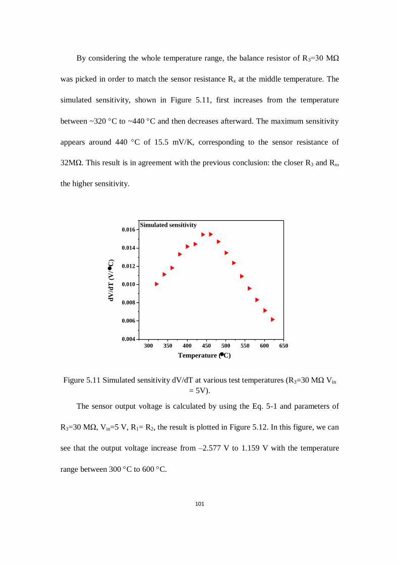
101
By considering the whole temperature range, the balance resistor of R3=30 MΩ
was picked in order to match the sensor resistance Rx at the middle temperature. The
simulated sensitivity, shown in Figure 5.11, first increases from the temperature
between ~320 C to ~440 C and then decreases afterward. The maximum sensitivity
appears around 440 C of 15.5 mV/K, corresponding to the sensor resistance of
32MΩ. This result is in agreement with the previous conclusion: the closer R3 and Rx,
the higher sensitivity.
300 350 400 450 500 550 600 650
0.004
0.006
0.008
0.010
0.012
0.014
0.016
Temperature (C)
dV
/dT
(V
/ C
)
Simulated sensitivity
Figure 5.11 Simulated sensitivity dV/dT at various test temperatures (R3=30 MΩ Vin
= 5V).
The sensor output voltage is calculated by using the Eq. 5-1 and parameters of
R3=30 MΩ, Vin=5 V, R1= R2, the result is plotted in Figure 5.12. In this figure, we can
see that the output voltage increase from –2.577 V to 1.159 V with the temperature
range between 300 C to 600 C.
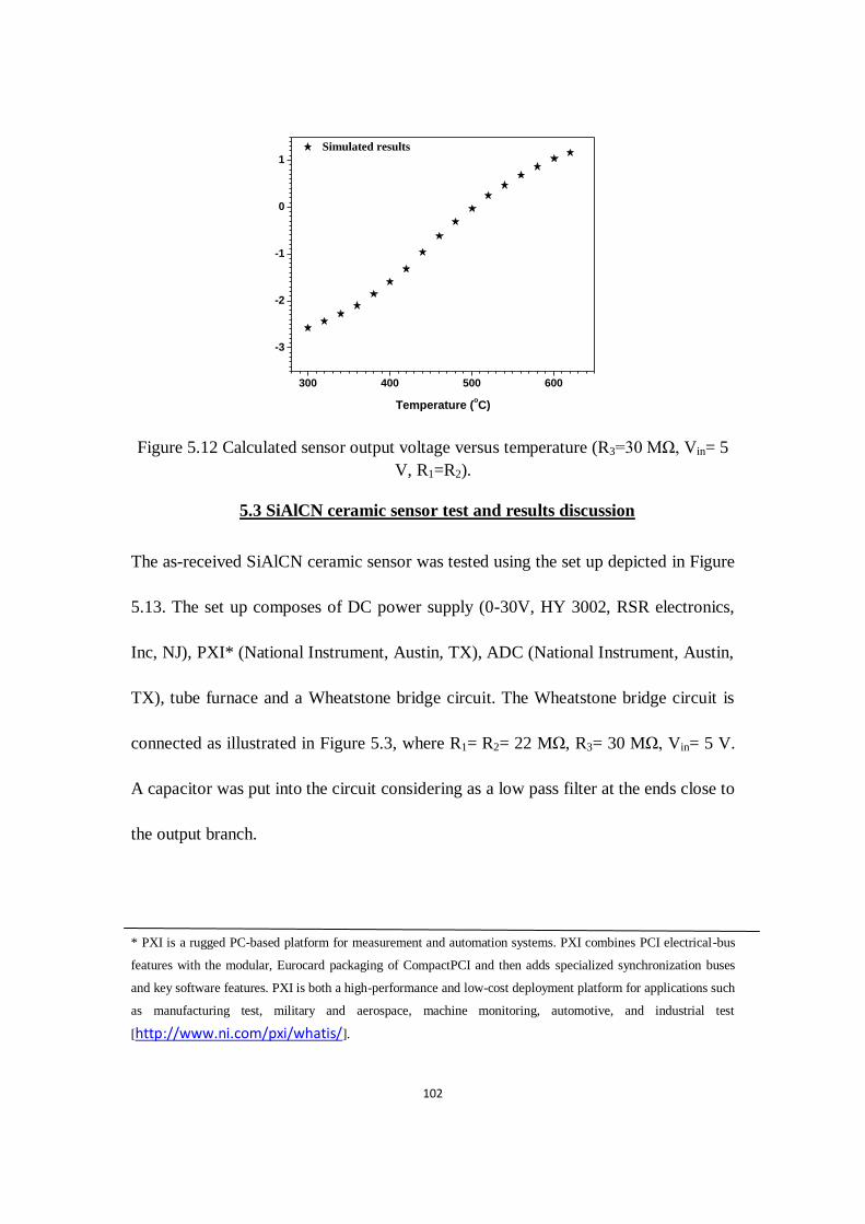
102
300 400 500 600
-3
-2
-1
0
1
Temperature (oC)
Simulated results
Figure 5.12 Calculated sensor output voltage versus temperature (R3=30 MΩ, Vin= 5
V, R1=R2).
5.3 SiAlCN ceramic sensor test and results discussion
The as-received SiAlCN ceramic sensor was tested using the set up depicted in Figure
5.13. The set up composes of DC power supply (0-30V, HY 3002, RSR electronics,
Inc, NJ), PXI* (National Instrument, Austin, TX), ADC (National Instrument, Austin,
TX), tube furnace and a Wheatstone bridge circuit. The Wheatstone bridge circuit is
connected as illustrated in Figure 5.3, where R1= R2= 22 MΩ, R3= 30 MΩ, Vin= 5 V.
A capacitor was put into the circuit considering as a low pass filter at the ends close to
the output branch.
* PXI is a rugged PC-based platform for measurement and automation systems. PXI combines PCI electrical-bus
features with the modular, Eurocard packaging of CompactPCI and then adds specialized synchronization buses
and key software features. PXI is both a high-performance and low-cost deployment platform for applications such
as manufacturing test, military and aerospace, machine monitoring, automotive, and industrial test
[http://www.ni.com/pxi/whatis/].

103
Figure5.13 SiAlCN sensor test set up and Wheatstone bridge circuit.
Before focusing on the sensor test, it is imperative to understand the effect of
capacitor as a low pass filter. The capacitor filter is one of the most simple and
common low pass filters commercially available. The relationship of the cutoff
frequency, effect resistance of the circuit and capacitance are satisfied with the
following equation of
, where f, Reff and C are the cutoff frequency, effect
resistance of the circuit and capacitance, respectively. It is clear that the larger
capacitance the smaller cutoff frequency and the better signal to noise ratio. In this
case the capacitance is selected of 1 F. And a smooth and low noise single was
achieved as the blue line shown in Figure 5.14.
The sensor performance was tested using the facilities mentioned above shown
in Figure 5.14. It can be seen that output voltage increases with increasing
temperature and the quality of the signal is rather smooth against very small noise. In
order to show a direct relationship between test temperature and output voltage, the
output voltage versus temperature is plotted in Figure 5.15. The results reveal that

104
output voltage increases nonlinearly with increasing temperature. This phenomenon is
due to the intrinsic conducting mechanism of the SiAlCN ceramics. As discussed
previously, the SiAlCN ceramic is an amorphous semiconductor with three possible
conducting mechanisms, It was determined previously, that the resistance change with
temperature should not linearly correlate and in turn implies that the output voltage
here is also nonlinear. In Figure 5.15 it can be observed that the calculated output
voltage, indicating by “*” , is agreement with the test results, approving a satisfactory
sensor design has been obtained.
0 500 1000 1500 2000 2500 3000
0
100
200
300
400
500
600
700
Time (s)
Tem
pera
ture (C
)
-3
-2
-1
0
1
2
Temperature (C)
Output voltage (V)
Ou
tpu
t v
olt
ag
e (
V)
Figure5.14 SiAlCN ceramic sensor output voltage and thermal couple reading VS
time.

105
0 100 200 300 400 500 600
-3
-2
-1
0
1
0 100 200 300 400 500 600
-3
-2
-1
0
1
Temperature (oC)
Experimental results
Simulated results
Ou
tpu
t v
olt
ag
e (
V)
Temperature (oC)
Figure 5.15 SiAlCN ceramic sensor output voltage (simulated and tested results).
The durability test of SiAlCN sensor was carried out by maintaining the
temperature of the sensor constant at ~510 C for more than 2 hours to observe the
change in output voltage shown in Figure5.16. It was found that the output voltage
remains constant until 30 min (Vout=1.00V) and then decreases gradually afterward by
0.02, 0.04 and 0.07 V for 1, 1.5 and 2 hours, respectively. This kind of drilling is
common if using capacitor as a low pass filter. The possible reason is because the
capacitor might be heated up during the test due to large current in the capacitor
branch. The capacitance changed because of the increasing temperature of capacitor.
A possible solution may include the use of a high quality capacitor or use of a low
pass filter instead of the capacitor.
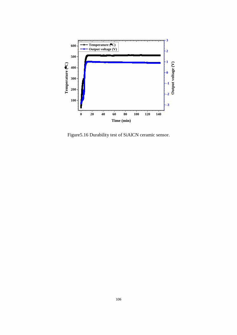
106
0 20 40 60 80 100 120 140
100
200
300
400
500
600
Temperature (C)
Output voltage (V)
Time (min)
Tem
pera
ture (C
)
-3
-2
-1
0
1
2
3
Ou
tpu
t v
olt
ag
e (
V)
Figure5.16 Durability test of SiAlCN ceramic sensor.

107
References:
1. Salah, T.B., S. Khachroumi, and H. Morel, Characterization, Modeling and
Design Parameters Identification of Silicon Carbide Junction Field Effect
Transistor for Temperature Sensor Applications. Sensors, 2010. 10(1): p. 388-
399.
2. Yang, J., A Silicon Carbide Wireless Temperature Sensing System for High
Temperature Applications. Sensors, 2013. 13(2): p. 1884-1901.
3. Wieczorek, G., et al. SiC Based Pressure Sensor for High-Temperature
Environments. in Sensors, 2007 IEEE. 2007.
4. Millan, J., et al. Electrical performance at high temperature and surge current of
1.2 kV power rectifiers: Comparison between Si PiN, 4H-SiC Schottky and JBS
diodes. in Semiconductor Conference, 2008. CAS 2008. International. 2008.
5. O''Brien, H., et al. Evaluation of Si and SiC SGTOs for High Action Army
Applications. in Electromagnetic Launch Technology, 2008 14th Symposium
on. 2008.
6. Sheikh, M. and N.A. Riza, Direct measurement high resolution wide range
extreme temperature optical sensor using an all-silicon carbide probe. Opt. Lett.,
2009. 34(9): p. 1402-1404.
7. Yonekubo, S., K. Kamimura, and Y. Onuma. Resistance-temperature
Characteristics Of Polycrystalline Sic/diamond Structure. in Solid-State Sensors
and Actuators, 1995 and Eurosensors IX.. Transducers '95. The 8th International
Conference on. 1995.

108
8. Liew, L.A., et al., Fabrication of SiCN ceramic MEMS using injectable
polymer-precursor technique. Sensors and Actuators a-Physical, 2001. 89(1-2):
p. 64-70.
9. Riedel, R., et al., A silicoboron carbonitride ceramic stable to 2,000 degrees C.
Nature, 1996. 382(6594): p. 796-798.
10. Wang, Z.C., F. Aldinger, and R. Riedel, Novel silicon-boron-carbon-nitrogen
materials thermally stable up to 2200 degrees C. Journal of the American
Ceramic Society, 2001. 84(10): p. 2179-2183.
11. An, L.N., et al., Silicoaluminum carbonitride with anomalously high resistance
to oxidation and hot corrosion. Advanced Engineering Materials, 2004. 6(5): p.
337-340.
12. Wang, Y.G., et al., Polymer-derived SiAlCN ceramics resist oxidation at 1400
degrees C. Scripta Materialia, 2006. 55(4): p. 295-297.
13. Wang, Y.G., et al., Oxidation of polymer-derived SiAlCN ceramics. Journal of
the American Ceramic Society, 2005. 88(11): p. 3075-3080.
14. Wang, Y.G., W.F. Fei, and L.N. An, Oxidation/corrosion of polymer-derived
SiAlCN ceramics in water vapor. Journal of the American Ceramic Society,
2006. 89(3): p. 1079-1082.
15. Bharadwaj, L., et al., Oxidation behavior of a fully dense polymer-derived
amorphous silicon carbonitride ceramic. Journal of the American Ceramic
Society, 2004. 87(3): p. 483-486.
109
16. Zhang, L.G., et al., A silicon carbonitride ceramic with anomalously high
piezoresistivity. Journal of the American Ceramic Society, 2008. 91(4): p.
1346-1349.
17. Ramakrishnan, P.A., et al., Silicoboron-carbonitride ceramics: A class of high-
temperature, dopable electronic materials. Applied Physics Letters, 2001.
78(20): p. 3076-3078.

110
CHAPTER SIX: CONCLUSION
Based on the discussion aforementioned, the following conclusions can be noted:
1. SiAlCN ceramics were synthesized using liquid precursor of polysilazane
(HTT1800) and aluminum-sec-tri-butoxide (ASB) as starting materials and
dicumyl peroxide (DP) as thermal initiator. The amorphous structure of as-
received ceramics is able to sustain to high temperatures (1500 C) without large
scale crystallization. The solid-state NMR indicates that SiAlCN ceramics have
the SiN4, SiO4, SiCN3, and AlN5 units. The Raman spectra reveals that SiAlCN
contains “free carbon” with the two specific peaks of “D” bond and “G” band at
1350 cm1
and 1600 cm1
, respectively. The “free carbon” becomes more and
more ordered with the increasing pyrolysis temperature. The EPR results show
that defects in the SiAlCN ceramic were related to carbon with a g-factor of
2.0016±0.0006. Defect concentration decreases with increasing sintered
temperature indicating that the degree of ordering of free carbon increases with
increasing temperature, which is consistent with the Raman spectra.
2. The electric and dielectric properties of SiAlCN ceramics were characterized. The
D.C. conductivity of SiAlCN ceramics increased with increasing sintered
temperature and the activation energy was about 5.1 eV, higher than that of SiCN
ceramics due to the presence of oxygen. The temperature dependent conductivity
indicates that the conducting mechanism is semiconducting band-gap model and
follows Arrhenius equation with two different sections of activation energy of
111
0.57 eVand 0.23 eV. The temperature dependent conductivity makes the SiAlCN
ceramic suitable for high temperature sensor applications. The dielectric
properties were carried out by using Agilent 4298A LRC meter. The results show
the dielectric constant and loss increase with increasing temperature and the
dielectric loss was dominated by the increasing of conductivity of SiAlCN
ceramics at high sintered temperature.
3. The SiAlCN ceramic sensor was fabricated by using the micro-machining method.
High temperature wired bonding issue was solved by the integrity embed method
(IEM). It was found that the micro-machining method is promising and cost-
effective way to fabricate PDC high temperature sensor and the IEM is satisfied to
solve the high temperature wire bonding problem with clear bonding interface
between the SiAlCN sensor head and the Pt wires. The Wheatstone bridge circuit
was well designed by considering the resistance relationship between the
matching resistor and the SiAlCN sensor resistor. It was found that the maximum
sensitivity can be achieved when the resistance of matching resistor is equal to the
SiAlCN sensor. The as-received SiAlCN ceramic sensor was tested up to 600 C
with the relative output voltage changing from -3.932 V to 1.153 V. The results
indicated that the output voltage is nonlinear with the temperature change; the test
sensor output voltage is consistent with simulated results. The durability test was
carried out at 510 C for more than two hours. It was found that the output voltage

112
remains constant for the first 30 min and then decreases gradually afterward by
0.02, 0.04 and 0.07 V for 1, 1.5 and 2 hours.
In summary, SiAlCN ceramics are synthesized with excellent
thermomechanical properties, such as high thermal stability, high
oxidation/corrosion resistance and high temperature multifunctionalities. SiAlCN
ceramic high temperature sensors have been fabricated and characterized at high
temperatures up to 600 C. The results indicate that the SiAlCN ceramic sensor is
suitable for high temperature and harsh environment application.

113
APPENDIX –A: CERAMIC NANOCOMPOSITES REINFORCED
WITH HIGH VOLUME FRACTION OF CARBON NANOFIBERS
114
Carbon nanofiber (CNF) reinforced polymer-derived silicon carbonitride
(SiCN) ceramic nanocomposite was fabricated by infiltrating CNF preform with
liquid-phased polymeric preceramic precursor following by pyrolysis. The composite
shows a very dense structure with a very high CNF concentration of 20 vol.%. The
mechanical properties were investigated by a microindentation technique. It is found
that the fracture mechanisms include crack branching, CNF bridging and CNF pullout,
which lead to the increase in the fracture energy of the nanocomposite as compared to
the monolithic SiCN. The indentation results also show that the indentation hardness
of the CNF-reinforced SiCN-nanocomposite is smaller than that for the monolithic
SiCN, indicating local softening of the nanocomposite.
1. Introduction
One-dimensional carbon nanostructures (e.g. nanotubes, nanowires and
nanofibers) have attracted extensive attentions due to their unique and often superior
properties as compared to bulk materials, thus promising for widespread applications.
For example, it has been demonstrated that carbon nanotubes (CNTs) possess strength
as high as 60 GPa [1, 2] and elastic modulus of the order of 1-5 TPa [3-6]. Depending
on the diameters and orientations of their hexagons with respect to the tube axis,
CNTs can be either semiconducting or metallic [7, 8]. The axial thermal conductivity
of CNTs is even higher than that of diamond [9]. It has also been demonstrated that
the strength and elastic modulus of silicon carbide (SiC) nanowires are also much
higher than those measured from bulk SiC [10]. While previous studies on one-

115
dimensional nanostructures were primarily focused on using them for a verity of
nano-devices, another equally important application of these materials is to make
multifunctional nanocomposites. It is expected that this new class of nanocomposites
could exhibit significantly improved mechanical as well as functional properties.
Application of one-dimensional nanostructures for ceramic matrix
nanocomposites has been attempted in the last decade or so, with the focuses on using
carbon nanotubes as the reinforcing phase. Majority of previous works synthesized
the nanocomposites by sintering the mixtures of CNTs and ceramic powder [11-13] or
ceramic powders with in-situ grown CNTs [14, 15]. The drawback of this technique is
that the uniform dispersion of CNTs in ceramic matrix is difficult to achieve. More
recently, CNT-ceramic nanocomposites were prepared by using polymer-derived
ceramic processing, in which the CNTs were first mixed with liquid-phased pre-
ceramic precursor followed by pyrolysis at elevated temperatures [16]. While the
relatively uniform dispersion of CNTs has been achieved, this technique cannot be
used to synthesize nanocomposites with high CNT concentrations.
In this work, we report a novel technique which can be used to synthesize
ceramic matrix nanocomposites reinforced with high concentration and uniformly
dispersed one-dimensional nanostructures. In this technique, one-dimensional

116
nanostructures were first made into a preform. The preform was then infiltrated with
liquid-phased pre-ceramic precursor followed by pyrolysis. While carbon nanofibers
(CNFs) are used as the reinforcing phase in this work, the technique developed can be
used for other one-dimensional nanostructures.
2. Experimental Procedures
Commercially available carbon nanofiber (PR-19, Pyrograf Products, Inc.
Cedarville, OH) with a diameter of ~100 nm and a length of 30-100 μm and a liquid-
phased polysilazane (VL20, Kion, Huntingdon Valley, PA) were used as the starting
materials; and poly (solium-4 styrene-sulfonate) (PS4SS, Sigma-Aldrich, Saint Louis,
MO) was used as the surfactant for CNF dispersion. In a typical process, 100 mg
CNFs and 200 mg PS4SS were mixed in 100 mL water by ultrasonication and
magnetic stirring for 2 hrs at room temperature. The as-received CNFs suspension
was poured onto a filter to remove the water with a vacuum to obtain a CNFs preform.
The thickness of the preform can be tailored by changing of the amount of CNFs
suspension. After drying at 120 oC for 8 hrs in vacuum, the CNFs preform was
infiltrated by VL20 with 4 wt% of dicumyl peroxide (Acros Organics, Morris Plains,
NJ) as the thermal initiator [17]. The infiltrated CNFs preform was solidified by heat-
treatment at 100 oC for 24 hrs and then pyrolyzed at 1000
oC in N2. For comparison,
the monolithic SiCN ceramic were also prepared using the same conditions.

117
The pyrolysis behavior of the as-received infiltrated preform was
characterized using thermal gravimetric analysis (TGA, SDT-Q600, TA Instruments,
New Castle, DE). The density of both composites and the monolithic SiCN were
measured using Archimedes’ principle. The microstructures of the composites were
observed using scanning electron microscopy (SEM, Zeiss ULTRA-55 FEG, Carl
Zeiss SMT AG Company, Oberkochen, Germany).
The mechanical behavior of the nanocomposite and pure ceramic was tested
using instrumented microindentation with Vickers indenter on a Micro-Combi Tester
(CSM Instruments, Peseux, Switzerland). The test was carried out under the load-
control mode with the indentation loads in the range of 1000 mN to 5000 mN. Prior to
a full indentation, a pre-load of 5 mN was applied to the indenter in order to maintain
intimate contact between the indenter and the surface of the sample and to avoid the
effect of impact. Both the loading time and unloading time were set to be 30 s without
intermediate holding at the peak indentation load. Five indents were made for each
indentation load.
3. Results and Discussion
Figure 1a is an optical microscopy image of the prepared CNF preform, which
is ~ 20 mm in length and ~ 1.5 mm in thickness. Figure 1b is a SEM image of the
preform, showing the uniform dispersion of CNFs. The preforms were infiltrated with
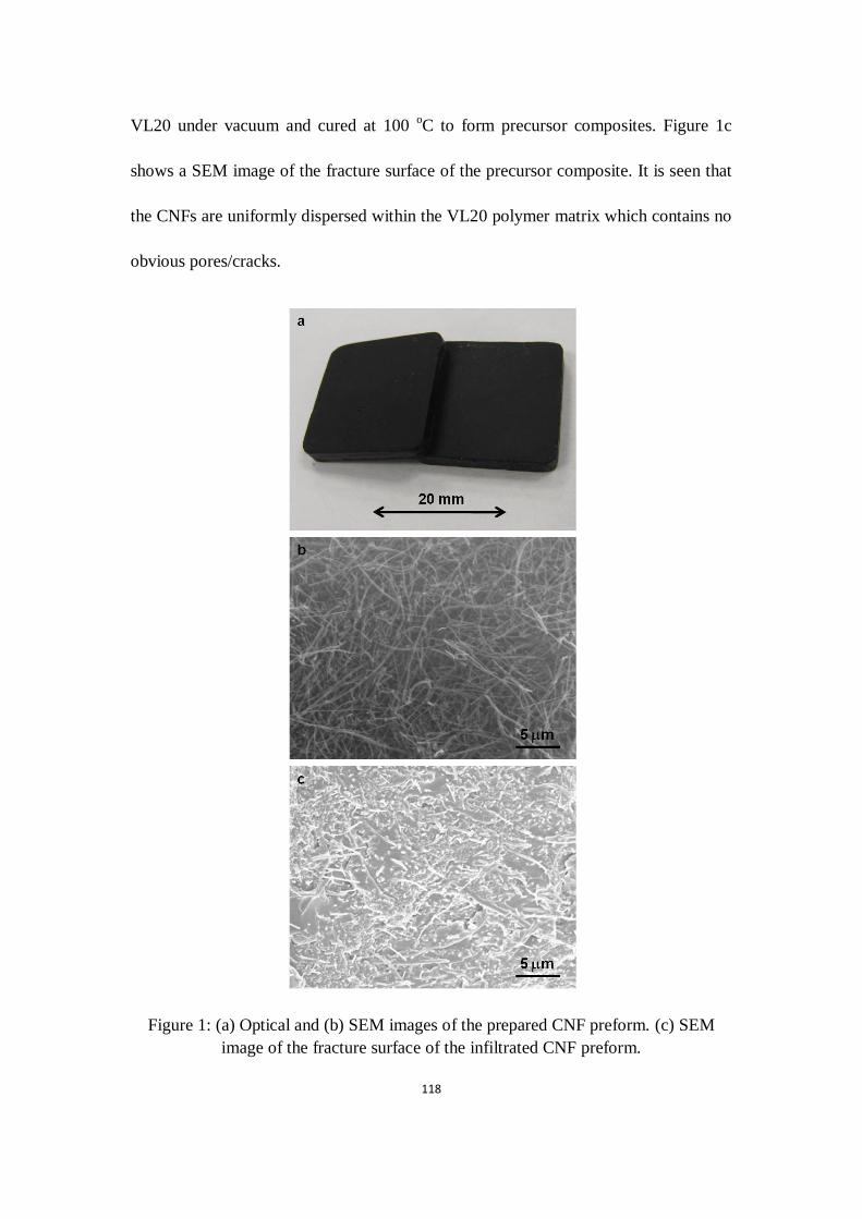
118
VL20 under vacuum and cured at 100 oC to form precursor composites. Figure 1c
shows a SEM image of the fracture surface of the precursor composite. It is seen that
the CNFs are uniformly dispersed within the VL20 polymer matrix which contains no
obvious pores/cracks.
Figure 1: (a) Optical and (b) SEM images of the prepared CNF preform. (c) SEM
image of the fracture surface of the infiltrated CNF preform.
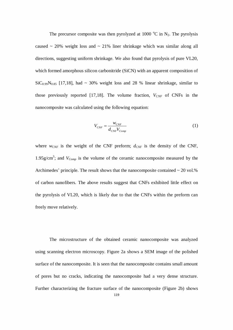
119
The precursor composite was then pyrolyzed at 1000 oC in N2. The pyrolysis
caused ~ 20% weight loss and ~ 21% liner shrinkage which was similar along all
directions, suggesting uniform shrinkage. We also found that pyrolysis of pure VL20,
which formed amorphous silicon carbonitride (SiCN) with an apparent composition of
SiC0.99N0.85 [17,18], had ~ 30% weight loss and 28 % linear shrinkage, similar to
those previously reported [17,18]. The volume fraction, VCNF of CNFs in the
nanocomposite was calculated using the following equation:
CompCNF
CNFCNF
Vd
wV (1)
where wCNF is the weight of the CNF preform; dCNF is the density of the CNF,
1.95g/cm3; and VComp is the volume of the ceramic nanocomposite measured by the
Archimedes’ principle. The result shows that the nanocomposite contained ~ 20 vol.%
of carbon nanofibers. The above results suggest that CNFs exhibited little effect on
the pyrolysis of VL20, which is likely due to that the CNFs within the preform can
freely move relatively.
The microstructure of the obtained ceramic nanocomposite was analyzed
using scanning electron microscopy. Figure 2a shows a SEM image of the polished
surface of the nanocomposite. It is seen that the nanocomposite contains small amount
of pores but no cracks, indicating the nanocomposite had a very dense structure.
Further characterizing the fracture surface of the nanocomposite (Figure 2b) shows

120
that the carbon nanofibers are uniformly dispersed within the ceramic matrix,
suggesting that the pyrolysis did not destroy the CNFs, neither disturb their
distribution. The image also reveals substantial pullout of nanofibers from the ceramic
matrix with the pullout length ranging from 1 to 5 micrometers. This result suggests
that the nanocomposite may have good fracture toughness.
Figure 2: SEM images of (a) polished surface and (b) fracture surface of the ceramic
nanocomposites.
Figure 3 shows typical indentation loading and unloading curves of the
nanocomposite. The loading curves for different indentation loads overlap, suggesting
that the loading rate has a negligible effect on the load–displacement relation. The
microhardness, vH , which is used to describe the plastic behavior of a material, is
calculated as
10 m
a
2 m
b

121
2
1.85v
FH
d (2)
where d is the average diagonal length of the impression, and F is the indentation load.
Using the measured diagonal lengths, one can calculate the microhardness by using
Eq. (2). The variation of the microhardness of the nanocomposite with the indentation
load is shown in Figure 4. For comparison, the corresponding microhardness of the
monolithic SiCN is also included. The microhardness of the nanocomposite is
9.52±0.86 GPa, which is less than 15.44±0.97 GPa for the monolithic SiCN. This
result suggests that the use of carbon nanofiber in SiCN caused softening in resisting
local plastic deformation. It is known that CNFs have higher modulus in the axial
direction, while they are very flexible in the transverse direction which provides less
resistant to the deformation in the transverse direction. In general, it is impossible to
make the CNF/SiCN nanocomposite with the CNFs’ aligning in one direction by
using the current technique. The CNFs form a fiber network with random distribution
of the CNFs’ direction. This is supported by the SEM micrograph (Figure 1b). The
random distribution of the CNFs reduces the possible enhancement of the CNFs to the
mechanical strength of the nanocomposite. In addition, the bonding strength between
the CNFs and the SiCN matrix plays an important role in controlling the mechanical
behavior of the CNF/SiCN nanocomposite. Quantitative assessment on the bonding
strength is needed in order to understand the effect of CNFs on the mechanical
strength of the nanocomposite and to interpret the microhardness behavior.
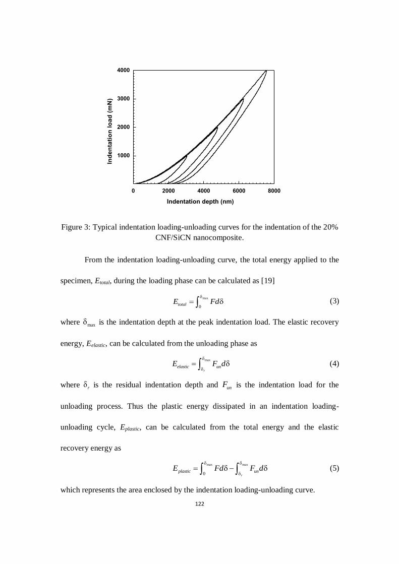
122
0 2000 4000 6000 8000
1000
2000
3000
4000
Ind
en
tati
on
lo
ad
(m
N)
Indentation depth (nm)
Figure 3: Typical indentation loading-unloading curves for the indentation of the 20%
CNF/SiCN nanocomposite.
From the indentation loading-unloading curve, the total energy applied to the
specimen, Etotal, during the loading phase can be calculated as [19]
max
0totalE Fd
(3)
where max is the indentation depth at the peak indentation load. The elastic recovery
energy, Eelastic, can be calculated from the unloading phase as
max
relastic unE F d
(4)
where r is the residual indentation depth and unF is the indentation load for the
unloading process. Thus the plastic energy dissipated in an indentation loading-
unloading cycle, Eplastic, can be calculated from the total energy and the elastic
recovery energy as
max max
0 rplastic unE Fd F d
(5)
which represents the area enclosed by the indentation loading-unloading curve.

123
1000 2000 3000 4000 50000
5
10
15
20
Mic
roh
ard
ne
ss
(G
Pa
)
Indentation load (mN)
SiCN
CNF/SiCN composites
Figure 4: Variation of the microhardness with the indentation load.
Figure 5 shows the dependence of the dissipated plastic energy on the residual
indentation load. It is seen that more energy is dissipated in the nanocomposite for the
same indentation load. This is in accord with the low microhardness of the
nanocomposite, which allows the indentation to produce more localized plastic
deformation and absorb more external energy due to the small transverse compliance
of CNFs. Using curve-fitting to fit the data points, one observes that the plastic energy
is proportional to the 3/2 power of the indentation load, similar to the results for the
indentation of aluminum [19, 20]. Even though the 3/2 power relation has been
derived from the cavity model and dislocation mechanics for the indentation of
crystalline metals [19], it is unclear why the indentation deformation of the monolithic
SiCN and CNF/SiCN nanocomposite also followed the same relationship.
124
0 1000 2000 3000 4000 5000
0
2
4
6
SiCN
CNF/SiCN composites
Indentation load (mN)
pla
sti
c e
ne
rgy
(J
)
Figure 5: Dependence of the plastic energy dissipated in an indentation loading-
unloading cycle on the indentation load.
Figure 6 shows the variation of the energy ratio, / plastic totalE E , as a function of
the indentation load for the monolithic SiCN and CNF/SiCN nanocomposite. The
energy ratio decreases with the increase of the indentation load, suggesting that less
portion of the indentation was dissipated in an indentation cycle for large indentation
loads. For small indentation load, more portion of the indentation energy was
dissipated in the nanocomposite than that in the monolithic SiCN. This implies that
the CNF/SiCN nanocomposite has higher toughness for small indentation loads than
the monolithic SiCN.

125
1000 2000 3000 4000 50000.30
0.35
0.40
0.45
0.50
SiCN
CNF/SiCN composites
Indentation load (mN)
Pla
sti
c e
ne
rgy
/ T
ota
l e
ne
rgy
Figure 6: Dependence of the energy ratio, / plastic totalE E , on the indentation load.
There are three obvious toughening mechanisms in the CNFs reinforced SiCN
ceramic composites: CNFs bridging, CNFs pullout and crack branch, as shown in
Figure 7. It is can be seen that an original crack source from the right hand side of
Figure 7a caused a main crack growth. The main crack was branched to two sub-
cracks. Furthermore, one of the sub-cracks was divided into other two sub-cracks.
This is a clearly crack branch toughening mechanism, which will increase the
toughness of the composites tremendously. The CNF bridging toughening mechanism
is also observed in the composites as shown in Figure 7a. Another toughening
mechanism of the CNFs pull out is coming out after the CNFs were broken shown in
Figure 7b. If the bonding force between the CNFs and the ceramic matrix is less than
the tensile strength of CNF, a debonding occurs at the interface of CNF and ceramic
matrix. In result, the CNF pullout occurred at one side of the crack and left a hole in

126
the opposite side (Figure 2b). If the bonding force is larger than the tensile strength,
the CNFs will be broken at the site of defects existed after the CNF bridging and both
sides showed the CNF pullout, no holess appear. Defects and low tensile strength
(compare to carbon nanotube) are the two main reasons of the short CNFs pullout
length [16].
Figure 7: SEM images showing (a) CNF bridging and crack branch (b) CNFs pull out.
4. Summary
In this paper, we develop a simple and unique processing technique for
making ceramic nanocomposites reinforced with high volume fraction of carbon
nanofibers. In this technique, the CNFs are first made into a preform, which is then
127
infiltrated with liquid-phase polymeric preceramic precursor. The infiltrated preform
is then pyrolyzed at 1000oC to convert the precursor to silicon carbonitride ceramic.
The obtained ceramic composite shows very high dense structure with small amount
of pores, but no cracks. The mechanical behavior of the nanocomposite is
characterized using instrumented microindentation. The results show that the hardness
of the nanocomposites decreases as compared to the monolithic ceramic due to the
flexibility of the carbon nanofibers. While the fracture energy of the nanocomposite
increases as compared to the monolithic ceramic. The three toughening mechanisms
are identified: CNFs bridging, CNFs pullout and crack branch. While the present
work focuses on CNFs, the developed technique is suitable for other nano-scaled
reinforcements.
References
1. M. Yu, O. Lourie, M.J. Dyer, K. Moloni, T. F. Kelly and R.S. Ruoff, ”Strength
and breaking mechanism of multiwalled carbon nanotubes under tensile load,”
Science 287, 637 (2000).
2. M. Yu, B.S. Files, S. Arepalli and R.S. Ruoff, “Tensile loading of ropes of single
wall carbon nanotubes and their mechanical properties,” Phys. Rev. Lett. 84, 5552
(2000).
3. B.I. Yakobson, C.J. Brabec and J. Bernhole, “Nanomechanics of carbon tubes:
instabilities beyond linear response,” Phys. Rev. Lett. 76, 2511 (1996).
128
4. G.V. Lier, C.V. Alsenoy, V.V. Doren and P. Geerlings, “Ab initio study of the
elastic properties of single-walled carbon nanotubes and graphene,” Chem. Phys.
Lett. 326, 181 (2000).
5. M.M.J. Treacy, T.W. Ebbesen and J.M. Gibson, “Exceptionally high Young’s
modulus observed for individual carbon nanotubes,” Nature (London) 381, 678-80
(1996).
6. O. Lourie and H.D. Wagner, “Evaluation of Young's modulus of carbon
nanotubes by micro-Raman spectroscopy,” J. Mat. Res. 13, 2418 (1998).
7. N. Hamada, S.I. Sawada and A. Oshiyama, “New one-dimensional conductors -
graphitic microtubules,” Phys. Rev. Lett. 68, 1579 (1992).
8. H. Dai, J. Kong, C. Zhou, N. Franklin, T. Tombler, A. Cassell, S. Fan and M.
Chapline, “Controlled chemical routes to nanotube architectures, physics, and
devices,” J. Phys. Chem. B 103, 11246 (1996).
9. S. Berber, Y. Kwon and D. Tomanek, “Unusually high thermal conductivity of
carbon nanotubes,” Phys. Rev. Lett. 84, 4613 (2000).
10. E.R. Wong, P.E. Sheehan and C.M. Lieber, “Nanobeam mechanics: elasticity,
strength, and toughness of nanorods and nanotubes,” Science, 277[36], 1971-75
(1997).
11. R. Ma, J. Wu, B. Wei, J. Liang and D. Wu, “Processing and properties of carbon
nanotubes-nano-SiC ceramic,” J. Mat. Sci. 33, 5243-46 (1998).

129
12. R.W. Siegel, S. Chang, B.J. Ash, J. Stone, P.M. Ajayan, R.W. Doremus and L.S.
Schadler, “Mechanical behavior of polymer and ceramic matrix nanocomposites,”
Scripta Mater. 44, 2061-64 (2001).
13. G. Zhan, J.D. Kuntz, J. Wan and A.K. Mukherjee, “Single-wall carbon nanotubes
as attractive toughening agents in alumina-based nanocomposites,” Nature Mat. 2,
38 (2002).
14. A. Peigney, Ch. Laurent, O. Dumortier and A. Rousset, “Carbon nanotubes-Fe-
alumina nanocomposites. Part I: Influence of the Fe content on the synthesis of
powder,” J. Euro. Ceram. Soc. 18, 1995-2004 (1998).
15. Ch. Laurent, A. Peigney, O. Dumortier and A. Rousset, “Carbon nanotubes-Fe-
alumina nanocomposites. Part II: Microstructure and mechanical properties of the
hot-pressed composites,” J. Euro. Ceram. Soc. 18, 2005-13 (1998).
16. L. An, W. Xu, S. Rajagopalan, C. Wang, H. Wang, Y. Fan, L. Zhang, D. Jiang, J.
Kapat, L. Chow, B. Guo, J. Liang and R. Vaidyanathan, “Carbon-nanotube-
reinforced polymer-derived ceramic composites,” Adv. Mater. 16, 2036-2040
(2004).
17. L. Bharadwaj, Y. Fan, L. Zhang, D. Jiang and L. An, “Oxidation behavior of a
fully dense polymer-derived amorphous silicon carbonitride ceramic,” J. Am.
Ceram. Soc., 87(3) 483-486 (2004).
18. A. Dhamne, W. Xu, B. Fookes, Y. Fan, L. Zhang, S. Burton, J. Hu, J. Ford and L.
An, “Polymer-ceramic conversion of liquid polyaluminasilazanes for SiAlCN

130
ceramics,” J. Am. Ceram. Soc., 88[9], 2415-19 (2005).
19. F.Q. Yang, L.L. Peng and K. Okazaki, “Microindentation of aluminum,”
Metallurgical and Materials Transactions A 35, 3323-3328 (2004).
20. F.Q. Yang, L.L. Peng and K. Okazaki, “Microindentation of aluminum processed
by equal channel angular extrusion,” J. Mater. Res.19, 1243-1248 (2004).

131
APPENDIX- B: FABRICATION OF NANO-SCALED POLYMER
DERIVED SIALCN CERAMIC COMPONENTS USING FOCUSED
ION BEAM

132
Fully dense polymer-derived SiAlCN ceramics were synthesized from
polysilazane as preceramic precursors followed by a thermal decomposition process.
The nanofabrication of amorphous SiAlCN ceramics was implemented with a focused
ion beam (FIB). FIB conditions such as the milling rate, the beam current, and the
number of passes were considered. It was found that nanopatterns with a feature size
of less than 100 nm could be fabricated onto polymer-derived ceramics (PDCs)
precisely and quickly. Specific nanostructures of thin walls, nozzle, and gear have
been fabricated as demonstrations that indicated the FIB technique was a promising
method to realize nanostructures on PDCs, especially for microelectromechanical
system (MEMS) and micro/nano sensor applications.
1. Introduction
Micro-sensors that can be operated in harsh environments are highly desired
for gas turbines, nuclear reactors, space vehicles and many other high-temperature
systems. Such sensors could be used to obtain useful information for monitoring the
operation processes and the health of hot-section structural components, for
improving the performance and safety of these systems. However, fabrication of such
sensors faces a huge technical challenge. The major hurdle is that the sensors must
survive harsh environments, including high temperatures, high stress, corrosive
species and/or radiation. In addition, the sensor materials must maintain specific
properties at high temperatures in order to provide means for sensing; and they must

133
do so in an easy-to-microfabricate way in order to lower costs. These requirements
basically prevent the use of most available materials.
Recently, polymer-derived ceramics (PDCs) have been considered as suitable
materials for making high-temperature microelectromechanical systems
(MEMS)/micro-sensors.[1]
Previous studies revealed that PDCs, synthesized from the
thermal decomposition of polymeric precursors, exhibit excellent thermomechanical
properties, such as high thermal stability,[2,3]
high oxidation/corrosion resistance[4-8]
and high temperature multifunctionalities.[9-12]
In addition, the direct polymer-to-
ceramic processing route of PDCs makes it much easier to be fabricated into various
components/devices with complex shapes/structures. Several techniques have been
developed for the fabrication of PDC-based MEMS and/or micro-sensors, such as
microcasting, lithography, micromachining, and direct writing.[13-16]
However, these
techniques can only be used to fabricate micro-scaled components. Given the
continuous demand for the downscaling of devices, it becomes crucially important to
develop techniques that can make components/devices from PDCs in the nanometer
scale.
In this paper, we report the fabrication of nanoscaled polymer-derived ceramic
components by using a dual-beam focused ion beam (FIB). It has been demonstrated
that FIB is a powerful tool for nanoscaled fabrications for many materials such as
metal,[17]
ferroelectrics,[18]
quartz,[19]
graphite,[20]
polydimethylsiloxane,[21]
glass
fiber,[22]
silicon, and germanium.[23]
To the authors’ knowledge, the use of FIB for
134
PDCs nanofabrication has not been reported yet. The FIB conditions, including the
milling rate, the beam current, and the numbers of passes, were taken into account for
precise and quick fabrication of PDCs on the nanoscale. The milling rate was
calculated based on the beam dwell time and the number of passes, and the milling
quality was monitored through a combination of scanning electron microscope (SEM).
Several specific nanofeatures, including thin wall (s), nozzle, and gear, were
demonstrated.
2. Experiments
In this study, polymer-derived amorphous silicoaluminum carbonitride
(SiAlCN) ceramics were used as the model material for studying and demonstrating
the feasibility of FIB-based nanofabrication of PDCs. Fully dense SiAlCN samples
were synthesized using commercially available liquid phase polysilazane (HTT1800,
Kion, Huntingdon Valley, PA) as the main precursor. Aluminum-tri-sec-butoxide
(ASB, Sigma-Aldrich, St. Louis, MO) and poly (melamine-co-formaldehyde)
acrylated solution (PVN, Sigma-Aldrich, St. Louis, MO) were used as the precursors
for Al and N, respectively. Bis (2, 4, 6-trimethylbenzoyl)-phenylphosphineoxide
(Irgacure 819, Ciba Specialty Chemicals Inc., Basal, Switzerland) was used as the
photoinitiator. These starting chemicals were reacted together to form photocurable
polyaluminasilazane using the following procedure. First, 7.8g HTT1800 and 1.0g
135
PVN were mixed together at 85oC for 10 min under magnetic stirring. 0.5g ASB and
0.5g 819 were then added into the mixture by stirring for additional 30 min at the
same temperature. The entire process was carried out using a standard Schlenk
technique in an ultrahigh purity (UHP) N2 environment instead of an atmosphere
environment to decrease the likelihood of contamination. The resultant
polyaluminasilazane was a clear, pale, yellow-colored liquid. The precursor was
vacuumed for 60 minutes and photopolymerized under a UV light for 20 minutes.
Afterwards, the SiAlCN ceramics were obtained by thermal decomposition set at
1000oC for 4 hours in a tube furnace with the presence of UHP N2
[24]. Finally, the
finished SiAlCN ceramics were polished on one side using diamond paste with a
particle size of 1 μm.
A dual-beam FIB instrument (FIB-SEM, Auriga series, Carl Zeiss) was
employed to perform the nanofabrication of the SiAlCN ceramics. The instrument
used a combination of SEM and FIB with two focused beams at a coincidence point.
In addition to SEM imaging, the instrument could rapidly mill materials via ion
sputtering or deposit material via chemical vapor deposition. The milling rate, beam
current and number of passes are key FIB parameters to be considered in order to
achieve the desired nanopatterns accurately and efficiently. The gallium ion energy
was set to the standard 30 keV because the scattering effects were negligible in the
cases described here. Depending on the nanopattern feature size, the beam spot
diameter was controlled between 3 nm ~ 59 nm, which was achieved by varying the

136
beam current between 1 pA ~ 600 pA. The milling rates and the milling quality under
different FIB conditions will be discussed in next section. Line scanning model and
spiral scanning model were generally used on rectangular shapes and circular shapes,
respectively. A 10 nm gold layer was coated onto SiAlCN ceramics in order to
improve the conductivity and to provide superior resolution. The SEM mode was used
to monitor the nanopattern features in situ with a 54° angle such that the feature size
was measured with an angle compensation method.
3. Results and Discussion
The core principle of the FIB milling technology is to operate the FIB with the
proper ion beam size and beam current to remove the required amount of material
from a predefined location in a controllable manner to obtain high-precision structures.
It is desired that the interaction between the incoming ions with the atoms near the
target surface leads to a collision cascade, known as sputtering, of the atoms. During
sputtering, a portion of the ejected atoms is frequently redeposited onto the sputtered
region such that it is difficult to control the amount of material removed from
sputtering. Both sputtering and redeposition are the governing effects in FIB milling
efficiency and milling accuracy. In order to ensure the milling efficiency, the beam
energy that is transferred from the ions to the target substrate should be high enough,
which means that the beam current is critical to the sputtering yield. In order to ensure

137
the milling accuracy, controlling the number of passes is important to prevent severe
redeposition.
To fully explore how the number of passes affects the milling quality
(represented by the bottom slope) and milling rate, sample trapeziums were milled
using different number of passes under the same FIB conditions. As shown in Figure
1 (a), (b), (c), and (d), the trapeziums were fabricated by the FIB using line scanning
model from bottom to top with same area and total milling time but with different
number of passes. The milled depth and bottom slope were calculated with an angle
compensation method from these images, which were taken by the SEM with 54°-tilt-
view. It is found that the number of passes directly affected the milling rate and
milling quality. It can be seen in Figure 1 (a) that there was a steep and rough bottom
with a maximum depth of 1.97 µm at the end of the milling for 1 pass. It is believed
that the material removed from the large milling depth was continuously redeposited
at the milled region that resulted in the inclined and rough bottom. A flatter and
smoother bottom with a small maximum milling depth of 0.53 µm was achieved when
the number of passes increased to 4 as shown in Figure 1(b). The similar flat and
smooth bottoms were observed with different maximum milling depth of 0.89µm and
1.48 µm for 9 passes and 15 passes, as shown in Figure 1(c) and (d), respectively. It
was found that a good milling quality can be achieved when there are no less than 4
passes. Therefore, 1 layer pass is suitable for high throughput milling that is less
concerned about the quality of the bottom pattern. However, for high precision
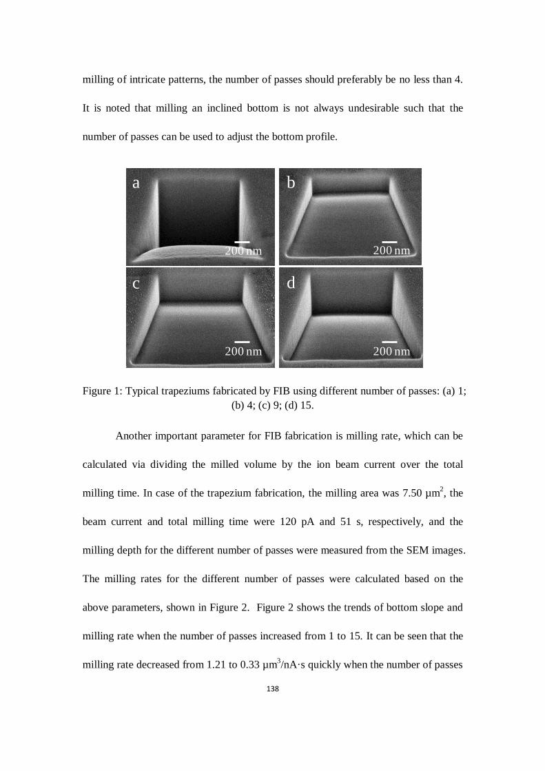
138
milling of intricate patterns, the number of passes should preferably be no less than 4.
It is noted that milling an inclined bottom is not always undesirable such that the
number of passes can be used to adjust the bottom profile.
Figure 1: Typical trapeziums fabricated by FIB using different number of passes: (a) 1;
(b) 4; (c) 9; (d) 15.
Another important parameter for FIB fabrication is milling rate, which can be
calculated via dividing the milled volume by the ion beam current over the total
milling time. In case of the trapezium fabrication, the milling area was 7.50 µm2, the
beam current and total milling time were 120 pA and 51 s, respectively, and the
milling depth for the different number of passes were measured from the SEM images.
The milling rates for the different number of passes were calculated based on the
above parameters, shown in Figure 2. Figure 2 shows the trends of bottom slope and
milling rate when the number of passes increased from 1 to 15. It can be seen that the
milling rate decreased from 1.21 to 0.33 µm3/nA·s quickly when the number of passes
200 nm200 nm
200 nm200 nm
a b
c d

139
increased from 1 to 4, and continued to increase afterwards. The trend of the milling
rate was nonlinear because removal of material in the milling process is mainly
determined by both sputtering and redeposition, of which the effects behave
nonlinearly when the number of passes is varied. Meanwhile, the bottom slope
dramatically decreased from 0.65 to 0.18 corresponding to the number of passes from
1 to 4, and then kept at 0.18 afterwards which was similar to what was observed in
Fig 1. The reason that the final slope was 0.18 and not 0 is due in large part to the
alignment error from the substrate surface to the FIB aperture. We conclude that the
number of passes should be no less than 4 in order to achieve sufficient milling
quality, and the more passes that is undergone, the higher the milling rate. One thing
should be mentioned here, there is a limit to the number of passes due to the minimum
dwell time limit of each pixel for each pass, which means that for smaller feature sizes,
they are limited by less number of passes.
Figure 2: The trends of bottom slope and milling rate with different number of passes
from 1 to 15.
0 2 4 6 8 10 12 14 160.0
0.2
0.4
0.6
0.8
1.0 Slope
Milling rate
Number of passes
Slo
pe
0.0
0.4
0.8
1.2
1.6
2.0
Mil
lin
g r
ate
(m
3/n
As
)

140
The beam current must also be addressed because it is highly related to the
milling quality and milling efficiency. A higher beam current is preferred for a higher
milling rate. Nevertheless, higher beam current results in a coarser milled structure
due to more debris being upheaved from the higher beam current and the larger beam
spot diameter. Typically, beam currents at less than 5 pA are selected for high
precision milling of nanoscale patterns, and beam currents at more than 600 pA are
selected for high throughput milling of micro-scale patterns. The milling rates of the
beam currents at 5 pA, 120 pA and 600 pA were measured with 1 pass, 4 passes, and
9 passes, as shown in Figure 3. With the same trend of the beam current at 120 pA,
the milling rates of beam currents at 5 pA and 600 pA decreased first, and then
increased when the number of passes increased from 4 to 9. The milling rate of the
larger beam current was higher than the smaller beam current, but the differences
were less than 30%, which indicated that the milling rates calculated before were
valid and may be referred for future fabrication of various patterns.
0 2 4 6 8 100.0
0.4
0.8
1.2
1.6
2.0
Mil
lin
g r
ate
(
m3/n
As
)
Number of passes
5 pA
120 pA
600 pA
Figure 3: Comparison of milling rates by using different FIB beam currents.
141
Several specific nanostructures of thin wall(s), nozzle, and gear were
fabricated onto SiAlCN ceramics using specially selected FIB conditions based on the
feature size. The thin, nano-scaled wall structure was fabricated by milling two
trapeziums to create a thin wall in between. The ion beam current of 600 pA with a
corresponding beam spot diameter of 59 nm was used to roughly cut a thin wall, as
shown in Figure 4(a). Since the bottom quality is less important in this case, the
number of passes was set to 1 for high throughput. The thin wall dimension in Figure
4(a) was about 850 nm in width, 8.5 µm in length, and more than 2 µm in depth.
Furthermore, a super-fine structure was achieved by precisely polishing the thin wall
incrementally with a beam current of 120 pA and a beam spot diameter of 25 nm. The
thickness of the thin wall was reduced to less than 100 nm, as shown in Figure 4(b).
As a result, an extremely high aspect ratio (> 20) was achieved that indicated the
process had great potential in nanosensor fabrication. A 1x13 thin wall array was
fabricated using the similar method, as shown in Figure 5(a). The wall thicknesses
and the spacing were between 200 nm ~ 350 nm. Figure 5(b) shows a close-up image
of the array, where the widths of the two thin walls were 240 nm and 320 nm
respectively.
142
Figure 4: (a) Rough cut of a thin wall with the dimension of 850 nm in width, 8.5 µm
in length, and more than 2 µm in depth; (b) Precise cut of a thin wall with the
thickness less than 100nm.
Figure 5: (a) Thin wall array; (b) Zoom-in thin wall array.
A nanonozzle was fabricated by using the spiral scanning model. As shown in
Figure 6(a), a nozzle with a 900 nm inner diameter and a 2100 nm outer diameter was
fabricated using a 600 pA beam current by milling away material to form a nozzle
ring area. Accounting for a 54º observation angle, shown in Figure 2(a), the height
can be calculated as 1.5 µm. A reverse nozzle with a 500 nm inside diameter and a
700 nm outside diameter was fabricated by using the same bitmap ring pattern and
milling away the nozzle ring area, as shown in Figure 6(b). It can be seen that the
patterns had an extremely smooth surface which affirmed the FIB technique as a good
candidate for PDCs nanofabrication.

143
Figure 6: (a) Nano-nozzle observed at a 54º tilted angle; (b) Reversed nano-
nozzle.
An intricate structure of a nanogear was fabricated to show the flexibility of
FIB. Gear structures are a challenge from a fabrication point of view because it is a
combination of circle wheel and rectangular teeth that are unlike a simple rectangular
utilized in thin walls and simple circle utilized in nozzles, and especially for a FIB
that is only capable to operate either the line scanning model or the spiral scanning
model for each milling process. For this case, the line scanning model was used for
each pattern scanning process due to the FIB limitation. The super-high FIB
magnification was used to ensure the ion beam spot diameter was less than half of the
bitmap pixel size in order to prevent discontinuity on the circle wheel surface. Figure
7(a) shows the fabricated nanogear with an extremely smooth surface and super
accurate gear wheel of ~ 2.5 µm in diameter and gear teeth of ~ 300 nm in width. An
even smaller feature size may be realized if a smaller beam current is applied instead
of 600 pA in this case. Another nanopattern with an “UCF” (short of University of
Central Florida) inscription was fabricated with a line width of less than 500 nm, as
shown in Figure 7(b).
144
Figure 7: Intricate PDCs nanostructures. (a) Nano gear and (b) nano letters.
4. Conclusions
FIB technique was demonstrated as a promising fabrication method for PDCs
on the nano scale and capable of extending existing applications, especially in MEMS
and micro/nano-sensor field. FIB conditions including the milling rate, the beam
current, and the number of passes were expressly selected for precise and efficient
nanofabrication of PDCs. A good milling quality was achieved by controlling the
number of passes to no less than 4, and the milling rate was observed to decrease first
in 1 to 4 passes and then continually increase afterward. The observed milling rates
under different FIB conditions may serve as reference for further fabrication of
various nanostructures on PDCs. The milling quality of various concave and convex
nanostructures was also illustrated. Several intricate PDC nanostructures such as thin
wall(s), nozzle, and gear were demonstrated. The feature size of nano-patterns may be
fabricated to less than 100 nm with an extremely smooth surface and super-high
accuracy.

145
Acknowledgements
The authors would like to thank the funding support from National Science
Foundation (MRI-R2: 0960022 and CMMI-0927441). The authors also appreciate Mr.
Christopher Santeufemio at the Campus Materials Characterization Laboratory
(CMCL) in the University of Massachusetts Lowell (UML) for his technical support
of using FIB.
References
1. L. Liew, W. Zhang, V. M. Bright, L. An, M. L. Dunn, and R. Raj, “Fabrication of
SiCN Ceramic MEMS Using Injectable Polymer-Precursor Technique,” Sensors
Actuators: A. Phys., 89 (1-2) 64-70 (2001).
2. R. Riedel, A. Kienzle, W. Dressler, L. Ruwisch, J. Bill, and F. Aldinger, “A
Silicoboron Carbonitride Ceramic Stable to 2000C,” Nature, 382, 796-8 (1996).
3. Z. C. Wang, F. Aldinger, and R. Riedel, “Novel Silicon-Boron-Carbon-Nitrogen
Materials Thermally Stable up to 2200oC,” J. Am. Ceram. Soc., 84, 2179-83
(2001).
4. L. An, Y. Wang, L. Bharadwaj, Y. Fan, L. Zhang, D. Jiang, Y. Sohn, V. Desai, J.
Kapat and L. Chow. Silicoaluminum carbonitride with anomalously high
resistance to oxidation and hot corrosion. Adv. Eng. Mater., 6[5], 337-40 (2004).

146
5. Y. Wang, Y. Fan, L. Zhang, W. Zhang, and L. An, “Polymer-Derived SiAlCN
Ceramics Resist Oxidation at 1400oC,” Scr. Mater., 55, 295-7(2006).
6. Y. G. Wang, L. An, Y. Fan and L. G. Zhang, S. Burton, Z. H. Gan, “Oxidation of
Polymer-Derived SiAlCN Ceramics,” J. Am. Ceram. Soc., 88 (11) 3075-3080
(2005).
7. Y. Wang, W. Fei, Y. Fan, L. Zhang, W. Zhang and L. An. A silicoaluminum
carbonitride ceramic resist oxidation/corrosion in water vapor. J. Mater. Res.,
21[7], 1625-1628 (2006).
8. L. Bharadwaj, Y. Fan, L. Zhang, D. Jiang and L. An. Oxidation behavior of a
fully dense polymer-derived amorphous silicon carbonitride ceramic. J. Am.
Ceram. Soc., 87(3) 483-486 (2004).
9. L. Zhang, Y. Wang, Y. Wei, W. Xu, D. Fang, L. Zhai, K. Lin, and L. An, “A
Silicon Carbonitride Ceramic with Anomalously High Piezoresistivity,” J. Am.
Ceram. Soc., 91, 1346-9 (2008).
10. P.A. Ramakrishnan, Y.T. Wang, D. Balzar, L. An, C. Haluschka, R. Riedel and A.
Herman. Silicoboron-carbonitride ceramics: A class of high-temperature, dopable
electronic materials. Appl. Phys. Lett., 78[20], 3076-78 (2001).
11. Hee- Yeon Ryu, Qi Wang and Rishi Raj. Ultrahigh-temperature semiconductors
made from polymer-derived ceramics. Journal of the American ceramic society,
vol. 93, no. 6, pp. 1668-1676, 2010.

147
12. K. Terauds, P. E. Sanchez-Jimenez, R. Raj, C. Vakifahmetoglu, P. Colombo.
Giant piezoresistivity of polymer-derived ceramics at high temperatures. Journal
of the European Ceramic Society, vol. 30, no. 11,pp. 2203-2207, 2010.
13. L. A. Liew, Y. Liu, R. Luo et al., “Fabrication of SiCN MEMS by
photopolymerization of pre-ceramic polymer,” Sensors and Actuators A: Physical,
vol. 95, no. 2–3, pp. 120-134, 2002.
14. L. Liew, W. Zhang, L. An et al., "Ceramic MEMS new materials, innovative
processing and future applications," American Ceramic Society bulletin. pp. 25-
30, 2001.
15. Y. Liu, L. A. Liew, R. Luo et al., “Application of microforging to SiCN MEMS
fabrication,” Sensors and Actuators A: Physical, vol. 95, no. 2, pp. 143-151, 2002.
16. H. Duan, C. Li, W. Yang, B. Lojewski, L. An and W. Deng. Near-field
electrospray printing of polymer-derived ceramics for micro-sensor applications.
Journal of Microelectromechanical Systems, accepted.
17. L. Ying-Yi, L. Jiunn-Der, J. Yu-Hung et al., “Focused ion beam-fabricated Au
micro/nanostructures used as a surface enhanced Raman scattering-active
substrate for trace detection of molecules and influenza virus,” Nanotechnology,
vol. 22, no. 18, pp. 185308, 2011.
18. R. Vanga, X. Huang, and Z. Zhou, “Focused ion beam fabricated bragg grating
filters in relaxor ferroelectrics,” Nuclear Instruments and Methods in Physics

148
Research Section B: Beam Interactions with Materials and Atoms, vol. In Press,
Corrected Proof, 2011.
19. L. D. Menard, and J. M. Ramsey, “Fabrication of Sub-5 nm Nanochannels in
Insulating Substrates Using Focused Ion Beam Milling,” Nano Letters, vol. 11,
no. 2, pp. 512-517, 2011.
20. G. Venugopal, M.-H. Jung, M. Suemitsu et al., “Fabrication of nanoscale three-
dimensional graphite stacked-junctions by focused-ion-beam and observation of
anomalous transport characteristics,” Carbon, vol. 49, no. 8, pp. 2766-2772.
21. G. Li, and et al., “The nanofabrication of polydimethylsiloxane using a focused
ion beam,” Nanotechnology, vol. 20, no. 14, pp. 145301, 2009.
22. C. Victor, and et al., “Optimized fabrication of curved surfaces by a FIB for
direct focusing with glass fibres,” Journal of Micromechanics and
Microengineering, vol. 19, no. 10, pp. 107003, 2009.
23. K. Miroslav, and et al., “Low energy focused ion beam milling of silicon and
germanium nanostructures,” Nanotechnology, vol. 22, no. 10, pp. 105304, 2011.
24. A. Dhamne, W. Xu, B. Fookes, Y. Fan, L. Zhang, S. Burton, J. Hu, J. Ford and L.
An. Polymer-ceramic conversion of liquid polyaluminasilazanes for SiAlCN
ceramics. J. Am. Ceram. Soc., 88[9], 2415-19 (2005).