Embed Size (px)
Citation preview

Development of high precision mechanical probes forcoordinate measuring machinesCitation for published version (APA):Pril, W. O. (2002). Development of high precision mechanical probes for coordinate measuring machines.Technische Universiteit Eindhoven. https://doi.org/10.6100/IR559401
DOI:10.6100/IR559401
Document status and date:Published: 01/01/2002
Document Version:Publisher’s PDF, also known as Version of Record (includes final page, issue and volume numbers)
Please check the document version of this publication:
• A submitted manuscript is the version of the article upon submission and before peer-review. There can beimportant differences between the submitted version and the official published version of record. Peopleinterested in the research are advised to contact the author for the final version of the publication, or visit theDOI to the publisher's website.• The final author version and the galley proof are versions of the publication after peer review.• The final published version features the final layout of the paper including the volume, issue and pagenumbers.Link to publication
General rightsCopyright and moral rights for the publications made accessible in the public portal are retained by the authors and/or other copyright ownersand it is a condition of accessing publications that users recognise and abide by the legal requirements associated with these rights.
• Users may download and print one copy of any publication from the public portal for the purpose of private study or research. • You may not further distribute the material or use it for any profit-making activity or commercial gain • You may freely distribute the URL identifying the publication in the public portal.
If the publication is distributed under the terms of Article 25fa of the Dutch Copyright Act, indicated by the “Taverne” license above, pleasefollow below link for the End User Agreement:www.tue.nl/taverne
Take down policyIf you believe that this document breaches copyright please contact us at:[email protected] details and we will investigate your claim.
Download date: 21. Jan. 2022

Development of
High Precision Mechanical Probes
for Coordinate Measuring Machines

CIP-DATA LIBRARY TECHNISCHE UNIVERSITEIT EINDHOVEN
Pril, Wouter O.
Development of High Precision Mechanical Probes for Coordinate Mea-suring Machines/by Wouter O. Pril. - Eindhoven : Technische UniversiteitEindhoven, 2002.Proefschrift. - ISBN 90-386-2654-1NUR 978Subject headings: high accuracy 3D probe system / probe; coordinate measur-ing machine / probe; CMM / probe; MEMS / probe; piezo resistive strain gauge
This thesis was prepared with Scientific Workplace v3.0
Printed by Ponsen & Looijen bv., Wageningen
Copyright c©2002 by W.O. Pril, Eindhoven, the Netherlands
This research was supported as ‘Nanoprobe Project’ by Mitutoyo Netherlands,Mitutoyo Japan, the Technology Foundation STW (project numbers: EWT55.3656 and EWT 66.4181) and the Dutch Metrology Institute NMi.
Development of
High Precision Mechanical Probes
for Coordinate Measuring Machines
P
ter verkrijging van de graad van doctoraan de Technische Universiteit Eindhoven
op gezag van de Rector Magnificus, prof.dr. R.A. van Santen,voor een commissie aangewezen door het College voor Promoties
in het openbaar te verdedigen opvrijdag 13 december 2002 om 16.00 uur
door
Wouter Onno Pril
geboren te Eindhoven

Dit proefschrift is goedgekeurd door de promotoren:
prof.dr.ir. P.H.J. Schellekensenprof.Dr.-Ing. L.M.F. Kaufmann
Copromotor:dr. H. Haitjema

Voor Anke


Summary
Due to the ever decreasing feature size and the associated tolerances on thedimensions, there is an increasing demand for high accuracy Coordinate Mea-suring Machines (CMM’s). Those machines need a probe system with an uncer-tainty substantially below 100 nm, while commercial high accurate probe sys-tems have uncertainties above a few hundred nanometre. This thesis describesthe design and verification of two probe systems to be used on high accurateCMM’s. The main requirements of the probe systems are an uncertainty of20 nm, and the possibility to use a 0.3 mm diameter spherical probe tip with-out damaging the workpiece. It is shown that the last mentioned requirementimplies that the suspended mass, i.e. any mass that is stiffly connected to theprobe, should be smaller than 20 mg, and that the stiffness of the suspensionshould be smaller than 200 N m−1.
The first probe system that has been designed is based on a so called Laser DiodeGrating Unit (LDGU) which is used in CD-players. The probe is suspended tothe probe house by three elastic elements each fixing one degree of freedom(DOF). This gives three DOF’s to the probe tip: translation in z-direction, andpseudo translation in x- and y-translation due to rotation around the end ofthe stylus that is fixed to the suspension. The LDGU is used to measure theprobe tip translation in z-direction. In principle it can also measure one of therotations, but it has been optimised to measure translation in z-direction.
The second probe system that has been designed uses a suspension comparableto the LDGU based probe system. It uses piezo-resistive strain gauges to mea-sure a 3D translation of the tip. The strain gauges are manufactured togetherwith their electrical connections and the elastic elements in a series of deposi-tion, lithography, and etching steps. The suspension strain gauge assembly canbe considered a Micro Electro Mechanical System (MEMS). Compared to theLDGU or other measurement systems that were considered, this approach hasthe advantage that no suspended mass is added and that few additional spaceis required.
A 1D calibration setup, called calibrator in this thesis, has been designed andrealised in order to test the uncertainty of both probe systems. The calibratoruses a differential plane mirror interferometer, based on a commercial availableangle interferometer, to measure the displacement of a piezo actuated mirror.
i

ii Summary
The calibrator has a 10 nm uncertainty, a 1 nm resolution, and a 30 µm range.It can be used for calibration of a wide range of high accurate length sensors,including roughness sensors. The instability and repeatability of the probe sys-tems have been tested in a dedicated setup without actuator and measurementsystem and with a short thermal loop.
The verification of the probe system based on strain gauges shows that theuncertainty is limited mainly by instability. The worst measured instability ina 60 hour interval is 30 nm. The standard deviation of the instability over allpossible one hour timespans is 8 nm. The one sigma repeatability of the probesystem is about 2 nm in x- and y-direction, and 0.7 nm in z-direction. Hysteresisis smaller than 10 nm for small (4 µm) moves and smaller than 20 nm for longermoves up to 25 µm. The one sigma reproducibility in calibration runs is 6 nm orsmaller. The instability of the sensitivity is 0.12%. In conclusion it can be statedthat the 20 nm uncertainty specification is met provided that the measurementis finished within 15 minutes.
The LDGU base probe system is verified in z-direction only. The worst caseinstability is measured to be 8 nm in a 120 hour measurement. The typical (onesigma) instability is 4 nm. The one sigma repeatability is 0.14 nm. Hysteresishas not been detected. A third order polynomial fit is needed to get the residualsbelow 1 nm. This probe system satisfies all requirements.
Summarising it can be stated that two probe systems based on new combina-tions of technology have been designed and that they meet the most importantspecifications. For the first time a MEMS has been successfully used in a CMMprobe system.
Samenvatting
Vanwege de alsmaar kleiner wordende dimensies van producten en de bijbe-horende toleranties, is er een toenemende vraag naar nauwkeurige CoordinatenMeetMachines (CMM’s). Deze machines hebben een tastsysteem nodig meteen onzekerheid die substantieel beneden de 100 nm ligt. Commercieel verkrijg-bare tastsystemen hebben een meetonzekerhied van tenminste enkele honderdennanometers. Dit proefschrift beschrijft het ontwerp en de verificatie van tweetastsystemen voor CMM’s met hoge nauwkeurigheid. De belangrijkste speci-ficaties zijn een onzekerheid van 20 nm en de mogelijkheid om een spherischeprobe tip te gebruiken met een diameter van 0.3 mm zonder dat het oppervlakvan het te meten werkstuk beschadigt. Aangetoond wordt dat de laatste eisbetekent dat de opgehangen massa, dat is alle massa die star verbonden is metde taster, kleiner moet zijn dan 20 mg en dat de stijfheid van de ophangingkleiner moet zijn dan 200 N m−1.
Het eerste tastsysteem dat is ontworpen, is gebaseerd op een ‘Laser Diode Grat-ing Unit’ (LDGU), die wordt gebruikt in CD-spelers. De taster is opgehangenaan het tasterhuis door middel van drie elastische sprieten die elk één vrijheids-graad vastleggen. Hierdoor resteren drie vrijheidsgraden voor de taster: trans-latie in z-richting, en pseudo-translatie in x- en y-richting door een rotatievrij-heid van de taster rondom het uiteinde dat bevestigd is aan de ophanging.De LDGU wordt gebruikt om de verplaatsing in z-richting van de tastertip temeten. In principe kan de LDGU ook één van de rotaties meten, maar de op-stelling is geoptimaliseerd voor het meten van z-translatie, waardoor geen hogenauwkeurigheid voor de rotatiemeting wordt verwacht.
Het tweede ontwikkelde tasterssysteem gebruikt een soortgelijke ophanging alshet LDGU-tastsysteem. Het gebruikt piezoresistieve reksensoren op de sprietenom een 3D verplaatsing van de tip te meten. De reksensoren worden samenmet hun electrische aansluitingen en de sprieten gezamenlijk vervaardigd doormiddel van een serie van depositie-, lithografie- en etsstappen. Een op derge-lijke manier vervaardigd product wordt ook wel een ‘Micro Electro MechanicalSystem’ (MEMS) genoemd. Vergeleken met de LDGU en andere overwogenmeetsystemen heeft deze aanpak het voordeel dat er geen extra opgehangenmassa wordt toegevoegd en dat er nauwelijks extra ruimte in het tasterhuisnodig is.
iii

iv Samenvatting
Een 1D kalibratieopstelling, in dit proefschrift ‘calibrator’ genoemd, is ontwik-keld om de meetonzekerheid van beide tastsystemen vast te stellen. De cali-brator is gebaseerd op een differentiële vlakke spiegel interferometer, waarbijgebruik is gemaakt van een commercieel verkrijgbare hoek interferometer. Eenpiëzo actuator zorgt voor een spiegelverplaatsing, die door de interferometergemeten wordt. De calibrator heeft een onzekerheid van 10 nm, een resolutievan 1 nm en een bereik van 30 µm. Hij is algemeen toepasbaar voor de kalibratievan lengtemeetsystemen met hoge nauwkeurigheid. Ook ruwheidssensoren kun-nen hiermee gekalibreerd worden. De herhaalbaarheid en instabiliteit van detastsystemen is vastgesteld in een aparte opstelling zonder actuator of meetsys-teem en met een korte thermische lus.
De verificatie van het tastsysteem met rekstroken toont aan dat de instabiliteitde grootste bijdrage aan de onzekerheid levert. De hoogste gemeten instabiliteitgedurende een 60 uur lange meting is 30 nm. De standaard deviatie van deinstabiliteit over alle mogelijke één uurs intervallen is 8 nm. De herhaalbaarheidvan het tastsysteem is 2 nm in x- en y-richting en 0.7 nm in z-richting. Dehysterese is kleiner dan 10 nm voor kleine (4 µm) bewegingen en kleiner dan20 µm voor grotere bewegingen tot 25 µm. De één sigma reproduceerbaarheidtijdens kalibratie metingen is 6 nm of kleiner. De stabiliteit van de gevoeligheidis 0.12%. Er kan worden geconcludeerd dat dit tastsysteem voldoet aan zijneisen, uitgezonderd de stabiliteit waardoor de duur van een meting beperkt istot 15 minuten.
Het LDGU tastsysteem is alleen in z-richting geverifieerd. De hoogste insta-biliteit in een 120 uurs tijdinterval is 8 nm. De typische (één sigma) insta-biliteit is 4 nm. De typische één sigma herhaalbaarheid is 0.14 nm. Hysteresisis niet waargenomen. Een derde graads polynoom moet worden gefit op de datateneinde het residu kleiner dan 1 nm te houden. Dit tastsysteem voldoet aanalle gestelde eisen.
Samenvattend kan worden gesteld dat twee op nieuwe technologiecombinatiesgebaseerde tastsystemen zijn ontwikkeld en dat beide voldoen aan de belang-rijkste specificaties. Niet eerder werd een MEMS succesvol gebruikt voor devervaardiging van een 3D CMM tastsysteem.

List of symbols,
terminology, and acronyms
Symbols
roman description and unit first used in
A matrix transforming a probe tip translation to a (2.16), (A.38)measurement vector [m]
aCMM CMM deceleration after a surface detection [m s−2] (2.8)ct probe tip stifness in a certain direction [Nm−1] (2.7), (3.9)cxy probe tip stifness in x- or y-direction [Nm−1] (3.6)cz probe tip stifness in z-direction [Nm−1] (A.13)d(t) combined indention of the probe tip and the (2.1)
workpiece as a function of time [m]E Young’s modulus [Nm−2] (2.2)Er reduced Young’s modulus [N m−2] (2.2)Es Young’s modulus of the slender rods [Nm−2] (2.25)f1 focal distance of the collimating lens [m] (3.2)f2 focal distance of the objective lens [m] (3.2)fn natural frequency [Hz] (3.9)Ft probing force [N] (2.4)FES Focal Error Signal [V] (3.1)G gauge factor of the strain gauges (2.17)ls length of the slender rod [m] (2.23)lst stylus length [m] (2.14)−→M measurement vector (2.15)m∗ equivalent mass [kg] (2.4)rt probe tip radius [m] (2.1)R resistance, mostly of a strain gauge [Ω] (2.17)RES Radial Error Signal [V] (3.3)Rx, Ry, Rz rotation around the x-, y-, and z-axis respectively -s3 smallest singular value of A [m] (2.17)
v

vi List of symbols, terminology, and acronyms
tr response time: time between the first work piece (2.8)contact of the probe tip and the CMM decelerationstart [s]
ts thickness of the slender rods [m] (2.24)Tx, Ty, Tz translation in x-, y-, and z-direction [m] -vimp maximum probing speed regarding impact (2.6)
force [m s−1]vovt maximum probing speed regarding overtravel (2.9)
force [m s−1]ws width of the slender rods [m] (2.27)xs x-distance of the free end of the slender rod to the (3.6)
stylus [m]Xovt overtravel of a CMM or admissable overtravel [m] (2.8), (3.8)Xt displacement of the probe tip [m] (2.1)ys y-distance of the free end of the slender rod to the (3.6)
stylus [m]
roman description and unit first used in
ε strain in the slender rods (2.27)ν Poisson’s ratio (2.2)νs Poisson’s ratio of the slender rods (3.6)σY yield strength [Nm−2] (2.2)
Terminology
The definition of some metrological terms as used in this thesis are copied fromthe International Vocabulary of Basic and General Terms in Metrology (VIM)[VIM 93]. For notes and examples, as well as for other terms, the reader isdeferred to this document.
measurementset of operations having the object of determining a value of a quantity
measurandparticular quantity subject to measurement
repeatability (of results of measurements)closeness of the agreement between the results of successive measurements ofthe same measurand carried out under the same conditions of measurement
reproducibility (of results of measurements)closeness of the agreement between the results of measurements of the samemeasurand carried out under changed conditions of measurement
uncertainty of measurementparameter, associated with the result of a measurement, that characterizes the

vii
dispersion of the values that could reasonably be attributed to the measurand
stabilityability of a measuring instrument to maintain constant its metrological charac-teristics with time
response timetime interval between the instant when a stimulus is subjected to a specifiedabrupt change and the instant when the response reaches and remains withinspecified limits around its final steady value
accuracy of a measuring instrumentability of a measuring instrument to give responses close to a true valueNOTE: “Accuracy” is a qualitative concept.
Abbreviations, acronyms
ADC Analog to Digital ConverterCMM Coordinate Measuring MachineCVD Chemical Vapour DepositionDOF Degree Of FreedomDVD Digital Versatile DiscEMC ElectroMagnetic CompatibilityFES Focal Error SignalLDGU Laser Diode Grating UnitLIGA LIthographie, Galvanoformung und Abformung, (lithography,
electroplating and moulding)LVDT Linear Variable Differential TransducerMEMS Micro Electro Mechanical SystemNA Numerical ApertureNMi Nederlands Meetinstituut (Dutch Metrology Institute)OPL Optical Path LengthPGA Programmable Gain AmplifierPSD Power Spectrum DensityRES Radial Error SignalRIE Reactive Ion EtchingSMD Surface Mounted DeviceSTW Stichting Technische Wetenschappen (Dutch Technology Foundation)SVD Singular Value DecompositionTTP Touch Trigger Probe


Contents
Summary i
Samenvatting iii
List of symbols, terminology, and acronyms v
1 Introduction 1
1.1 Coordinate measuring machines . . . . . . . . . . . . . . . . . . . 1
1.2 Probe systems . . . . . . . . . . . . . . . . . . . . . . . . . . . . . 4
1.3 Research objectives and thesis outline . . . . . . . . . . . . . . . 7
2 Design considerations 9
2.1 Choice of probe system type . . . . . . . . . . . . . . . . . . . . . 9
2.2 Probing forces . . . . . . . . . . . . . . . . . . . . . . . . . . . . . 10
2.2.1 Probing strategy . . . . . . . . . . . . . . . . . . . . . . . 10
2.2.2 Admissable probing force . . . . . . . . . . . . . . . . . . 13
2.2.3 Impact force . . . . . . . . . . . . . . . . . . . . . . . . . 14
2.3 Suspension . . . . . . . . . . . . . . . . . . . . . . . . . . . . . . 17
2.4 The measurement system . . . . . . . . . . . . . . . . . . . . . . 22
2.4.1 Optical sensors . . . . . . . . . . . . . . . . . . . . . . . . 23
2.4.2 Capacitive sensors, strain gauges, and inductive sensors . 25
2.4.3 Choice of measuring system . . . . . . . . . . . . . . . . . 32
ix

x Contents
3 Design of a 2D optical probing system 33
3.1 The Laser Diode Grating Unit (LDGU) . . . . . . . . . . . . . . 33
3.1.1 Measuring the z-translation of the probe . . . . . . . . . . 34
3.1.2 Measuring x-translation of the probe . . . . . . . . . . . . 37
3.1.3 Cross talk between z- and x-measurement . . . . . . . . . 38
3.2 Design of probe and suspension . . . . . . . . . . . . . . . . . . . 39
3.3 Electronics . . . . . . . . . . . . . . . . . . . . . . . . . . . . . . 42
3.4 Mechanical design and realisation . . . . . . . . . . . . . . . . . . 44
4 Development of a 3D probe system using strain gauges 47
4.1 Introduction to micromachining . . . . . . . . . . . . . . . . . . . 47
4.1.1 Bulk micromachining . . . . . . . . . . . . . . . . . . . . . 48
4.1.2 Surface micromachining . . . . . . . . . . . . . . . . . . . 48
4.1.3 Mould micromachining . . . . . . . . . . . . . . . . . . . . 48
4.2 Design of the probe and the suspension . . . . . . . . . . . . . . 49
4.3 Electronics . . . . . . . . . . . . . . . . . . . . . . . . . . . . . . 52
4.4 Realisation . . . . . . . . . . . . . . . . . . . . . . . . . . . . . . 55
4.4.1 Probe house . . . . . . . . . . . . . . . . . . . . . . . . . . 55
4.4.2 Photolithography and etching of the suspension, straingauges, and electrical connections . . . . . . . . . . . . . . 55
4.4.3 Assembling . . . . . . . . . . . . . . . . . . . . . . . . . . 58
5 Verification of both probe systems 61
5.1 Design of the calibrator . . . . . . . . . . . . . . . . . . . . . . . 62
5.1.1 The plane mirror differential laser interferometer setup . . 64
5.1.2 Mechanical construction . . . . . . . . . . . . . . . . . . . 72
5.1.3 Error analysis of the calibration setup . . . . . . . . . . . 76
5.2 Verification of the piezo-resistive probe system . . . . . . . . . . 82
5.2.1 Electric characterisation . . . . . . . . . . . . . . . . . . . 82
5.2.2 Displacements measurements . . . . . . . . . . . . . . . . 83
5.2.3 Stability measurements . . . . . . . . . . . . . . . . . . . 93
5.2.4 Discussion of the stability data . . . . . . . . . . . . . . . 95

Contents xi
5.3 Verification of the optical probe system . . . . . . . . . . . . . . 97
5.3.1 Displacement measurements . . . . . . . . . . . . . . . . . 97
5.3.2 Stability measurements . . . . . . . . . . . . . . . . . . . 100
5.3.3 Discussion of the verification of the optical probe system . 101
5.4 Summary . . . . . . . . . . . . . . . . . . . . . . . . . . . . . . . 102
6 Conclusions and recommendations 103
6.1 Conclusions . . . . . . . . . . . . . . . . . . . . . . . . . . . . . . 103
6.2 Recommendations . . . . . . . . . . . . . . . . . . . . . . . . . . 105
A Calculations on the suspension 107
A.1 Stiffness of the suspension . . . . . . . . . . . . . . . . . . . . . . 108
A.1.1 Stiffness of a slender rod . . . . . . . . . . . . . . . . . . . 108
A.1.2 Calculation of forces and moments . . . . . . . . . . . . . 110
A.2 Stresses in the slender rods . . . . . . . . . . . . . . . . . . . . . 111
A.3 Admissable overtravel computation . . . . . . . . . . . . . . . . . 113
A.4 Relating strain gauge data to displacements . . . . . . . . . . . . 115
B Dependence of the focal and radial error signals on the optics 119
B.1 Dependence of the focal error signal on the optics . . . . . . . . . 119
B.2 Dependence of the radial error signal on the optics . . . . . . . . 124
C Error analysis of the LDGU probe system 127
C.1 Errors in z-direction . . . . . . . . . . . . . . . . . . . . . . . . . 127
C.2 Errors in x-direction . . . . . . . . . . . . . . . . . . . . . . . . . 131
D Micromaching process of the suspension and measurementsystem 133

xii Contents
E Error analysis of the probe system based on strain gauges 139
E.1 Mechanical effects . . . . . . . . . . . . . . . . . . . . . . . . . . 139
E.1.1 Thermal expansion . . . . . . . . . . . . . . . . . . . . . . 139
E.1.2 Mechanical stability of glue . . . . . . . . . . . . . . . . . 140
E.2 Self heating of the strain gauges . . . . . . . . . . . . . . . . . . . 140
E.3 Intrinsic errors of the piezo resistors . . . . . . . . . . . . . . . . 144
E.4 Evaluation of the electronics . . . . . . . . . . . . . . . . . . . . . 144
E.4.1 Errors in the preamplifier . . . . . . . . . . . . . . . . . . 145
E.4.2 Other electronic error sources . . . . . . . . . . . . . . . . 147
E.5 Summary . . . . . . . . . . . . . . . . . . . . . . . . . . . . . . . 147
F Analyses of the A-matrix fit procedure 149
Bibliography 159
Acknowledgements 165
Curriculum Vitae 166
Chapter 1
Introduction
In both manufacturing and measuring technology an ongoing trend for higheraccuracies can be seen. Taniguchi noticed this trend [Taniguchi 83] and extrap-olated it to the future, well predicting the present state of the art in precisionengineering [Schellekens 98]. Especially during the last three decades, advancesin IC-technology pushed the state of the art forwards. Also in consumer elec-tronics precision techniques found their way, e.g. in video players, CD and itssuccessor DVD (digital versatile disc), and hard disks.
Together with the increasing precision of products, the need for highly accuratedimensional inspection increases. A Coordinate Measuring Machine (CMM) isoften used to accomplish this task. Recently the uncertainty1 of these machineshas entered the sub micrometre regime and further effort is done to decreaseit further [Vermeulen 99], [Ruijl 01]. 3D Probe systems are used to detect thesurface of the workpiece accurately. However, probe systems with an uncertaintysubstantially below a few tenths of a micrometre, are not available. The goal ofthis research is to develop such probe systems.
1.1 Coordinate measuring machines
A CMM is used to measure the geometry of objects. It is often preferred aboveother length measuring tools because of its versatility, ease of use, and its uncer-tainty which is nevertheless a few micrometres only. A probe system, attachedto the CMM, can be moved in a well known way in a certain measuring volume.It can be actuated either manually or by servo motors. Servo controlled axesgive better reproducing probing, and therefore higher accuracy, and possibil-ities for automation. To enable 3D displacement three independent axes are
1Terms like uncertainty, accuracy, and repeatability are defined as given in the Guide tothe expression of uncertainties in measurement [GUM 95]
1

2 Chapter 1. Introduction
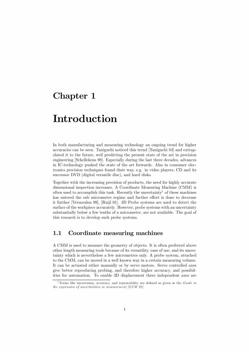
Figure 1.1: Prediction of future machining accuracy [Taniguchi 83].
necessary. In principle these can be linear or rotary axes, but three mutuallyorthogonal linear axes is the most common arrangement, e.g. as shown in figure1.2. Each axis consists of a guideway, a carriage that can move along the guide-way, a measurement system, mostly a linear scale, and an actuator, if the axisis servo controlled. The probe system is used to establish measurement pointson the work piece. Whenever the probe detects a surface, the CMM records thecoordinates of the probe by measuring the position of the axes. In some cases,the deflection of the probe tip is added to this position. The CMM softwarecorrects for the dimensions of the probe tip.
With the increased need for precision products and the improved manufactur-ing possibilities —e.g. Single Point Diamond Turning— the desired accuracy forCMM’s increased. Unfortunately, getting a high overall accuracy puts high de-mands on the individual elements in the structural loop. This is why even themost accurate commercially available CMM still has a measuring uncertaintyof about 0.5 m in a volume of some cubic decimetre. Larger machines, up tosome cubic metres, have larger uncertainties.

1.1. Coordinate measuring machines 3
z x
carriages
x-guideway
y-support
y-guideway
probe system
workpiece
table
y
z-guideway
Figure 1.2: Example of a Co-ordinate Measuring Machine.
Accuracy can be improved in two ways. On the one hand by software errorcompensation and on the other hand by developing inherently more accuratemachines. If errors repeat, it can be tried to model them in order to predict themas function of position, temperature distribution, and dynamics. This way themeasured coordinates can be corrected by subtraction of the expected error.Lot of effort has been done in this field [Sartori 95], [Soons 93], [Spaan 95],[Ruijl 01], [Florussen 02].
There are limits on software error compensation. Only part of the errors repeatsand other errors are hard to model e.g. errors due to thermal and dynamic ef-fects. For further decrease of the CMM uncertainty an inherently more accuratedesign should be made. Several attempts are being made to decrease the un-certainty to 100 or 50 nm, at the expense of a smaller measurement volume of acubic decimetre or less: Vermeulen developed a CMM with a 100∗100∗100 mm3
measuring volume, paying special attention to the suppression of thermal andAbbe errors2 [Vermeulen 98], [Vermeulen 99]. The two horizontal (x- and y-)scales in his design are moving together with the probe system, so that theprobe system is always in line with the x- and y-scales and consequently theAbbe principle is partly obeyed. Ruijl designed a CMM where the workpieceis moved instead of the probe system [Ruijl 01]. In this way it is possible tomeasure the displacement of the workpiece by three orthogonally aligned length
2The Abbe principle is defined as ‘The measuring instrument is always to be constructedthat the distance being measured is a straight line extension of the graduations on the scalethat serves as the reference’ [Schellekens 98]. An error due to a violation of the Abbe principleis called an Abbe error.

4 Chapter 1. Introduction
measuring interferometer systems which are all in line with the probe system.This CMM completely fulfills the Abbe principle. Peggs et al. extended a com-mercial CMM with a 6D interferometric measurement system which accuratelydetermines the probe position relative to the workpiece [Peggs 99]. They nec-essarily have to measure all degrees of freedom of the probe system, as theirdesign does not obey the Abbe principle.
Yet more accurate CMM’s have been or are being designed. The MolecularMeasuring Machine, designed at the United States National Institute of Stan-dards and Technology, is worth mentioning here. It uses a Scanning tunnelingMicroscope tip for surface detection and has shown atomic resolution in a vol-ume of 50 mm * 50 mm * 5 µm [Kramar 98]. Hocken, Trumper and others[Hocken 01] are designing their Sub-Atomic Measuring Machine (SAMM) witha measurement volume of 25 ∗ 25 ∗ 0.1 mm3.
1.2 Probe systems
The purpose of a probe system is to detect the surface of the workpiece to bemeasured. The detection is performed by mechanical touching, or by opticalmethods (such as triangulation probes and CCD cameras). Optical probe sys-tems are not part of research in this thesis. Mechanical probe systems can befurther divided into touch trigger and measuring probe systems. The latterare also called analogue probe systems. Both kinds of probe systems will bediscussed only shortly here. More information, including a patent search, canbe found in [Vliet 96].
The touch trigger probe was introduced by Renishaw in the early seventies. Assoon as the stylus is moved from its zero position, the resistance of an electricalcircuit is altered. At that moment the scales of the CMM are read. An exampleof such a probe system is shown in figure 1.3. Nowadays touch trigger probeshave better mechanisms for detecting a probe displacement, which increasedtheir uncertainties to a few tenths of a micrometre.
Measuring or analogue probe systems measure the probe tip position continu-ously. After a surface detection the CMM is stopped and controlled by signalsof the probe system to reach a pre-set probing force. In order to get the mostaccurate measurement point, the deflection of the probe is added to the positionof the CMM. This technique leads to a significant decrease of the uncertainty.In most commercial analogue probe systems both the measuring system, as thesuspension of the stylus have a larger mass compared to the touch trigger probe.Therefore the probing speed must be lowered in order to prevent intolerable highforces at the moment of probing. Also the controlling sequence takes some time,so probing is more time-consuming than in the touch trigger case.A basic principle of an analogue probe system is shown in figure 1.4.
Van Vliet explained in his thesis how the advantages of both principles can becombined to get a fast and accurate probe system. He developed an analogue

1.2. Probe systems 5
stylus carrier
(detachable)
probe tip
stylus
probe house
preload spring
carrier support
trigger circuit
Figure 1.3: Basic principle of a touch trigger probe system [Vliet 96].
probe system which is intended to get its measurement points short after the firstmoment of probing, like touch trigger probes. The advantage of this strategy is afast measurement procedure at a moment when the CMM is not yet decelerating,which limits the dynamic errors of the CMM. The stylus and the moving partof the measurement system should be light in order to prevent unacceptablyhigh dynamic impact forces due to the high probing speeds. The time availableto take a measurement point is limited because the CMM is still moving atthat moment. This means that the measurement system should be fast. Ingeneral fast measurements are difficult because of noise. Van Vliet solved theseproblems by using a single stage elastic suspension and an optical, triangulationbased measurement system. The basic setup of the probe system is shown infigure 1.5. The uncertainty varies from less than 0.5 µm at a probing speed ofless than 20 mm s−1 to 1.5 µm for a probing speed of 70 mm s−1. Even at thehighest speed no permanent indentions on an aluminum test specimen could befound.
When designing for high accuracy the same problems as described above haveto be solved. Often speed can be exchanged for accuracy: because more time isavailable, a part of the noise of the measuring system can be filtered. Also theneed for a light weight construction is shared. To enable the measurement ofsmall holes the probe ball should be small which caused high dynamic probingforces unless the mass of the stylus is small. Because of these similarities, theresearch described in this thesis can be seen as a continuation of van Vliet’swork. For highest accuracy the CMM should be at rest at the moment ofprobing, so van Vliet’s strategy can not be applied here.
Recently other probe systems were developed. Peggs et al. designed a probe sys-tem based on capacitive sensors to be used with his modified CMM [Peggs 99].

6 Chapter 1. Introduction
automatic loadcompensationmechanism
y-guideway
z-guideway
x-guideway
stylus
stylus carrier
Figure 1.4: Basic principle of an analogue probe system manufactured by Zeiss[Vliet 96]. It consist of three orthogonal elastic straight guiding mechanisms.Each guideway is to be equiped with a 1D measurement system (not drawn).
2D-detector
frame
light source
stylus carrier
stylus carriersuspension
mirror
stylus
y
z
x
light beam
Figure 1.5: Basic setup of van Vliet’s probe system.

1.3. Research objectives and thesis outline 7
They claim a resolution of 3 nm, a working range of ± 20 µm, and an equalstiffness in all three directions of approximately 10 N m−1. The total suspendedmass is 370 mg. Schwenke et al. designed a probe system where the position ofthe probe tip is directly measured by optical means [Schwenke 01]. They claima standard deviation of 200 nm for a 3D measurement on a calibration sphere.Takaya et al. designed a probe system intended for measurement of micro ma-chined parts [Takaya 99]. Instead of a stylus, they used a 10 µm diameter spheretrapped by a laser beam. The 3D position of the sphere is measured by a Linnikmicroscope interferometer. They expect to achieve a resolution of 30 nm. Hi-daka designed a new probing system intended for use at high measuring speed(30 mm s−1). They expect to reach a probing uncertainty of 210 nm.
1.3 Research objectives and thesis outline
The main goal of the research described in this thesis, is the development ofa probe system for CMM’s with an uncertainty of 100 nm or less. The probeuncertainty should be substantially smaller, because it is only part of the errorbudget of the CMM. It is set to 20 nm, assuming a room temperature stabilityof ± 0.1 K.
Besides this there are other requirements that should be met to a certain de-gree. The accessibility of the probe is very important as it will limit the utilityof the system in some cases. The accessibility is determined by a number ofparameters. A large tip will limit the interior measurement of small holes; us-ing 0.3 mm diameter spheres should be possible. A short stylus will restrictmeasurements of deep structures; the stylus length should therefore be at least4 mm. A large probe house width (compared to the stylus length) will limit thevisibility of the tip; the width of the probe house should be smaller than twotimes the stylus length. Another point of interest is the average time needed toperform a measurement. It consist of a pre-trigger period in which the CMMmoves with its probing speed, a feedback period in which the CMM is deceler-ated, and a period for taking the actual measurement. The length of the firstperiod is determined by the probing speed which should be as high as possible.However, large probing speeds increase the impact forces, especially when smallprobe tips are used. At a reasonable probing speed of 1 mm s−1 the dynamicprobing forces should be small enough to prevent damaging of the work piece.The length of the second period is determined by the dynamics of the CMMand is regarded as given data. The length of the third period is determinedby the speed of the measurement system and should be no more than a fewseconds. The measurement range of the probe system should be large enoughto overcome the overtravel of the CMM when moving with a probing speed of1 mm s−1. Overtravel is defined as the distance a CMM travels after a stopsignal has been given. Next to this, the absolute range of the probe systemshould be large enough to withstand an unintended hit of the probe when theCMM is moving at maximum speed. It is assumed that 0.5 mm is sufficient, or

8 Chapter 1. Introduction
else the maximum speed should be limited. Finally the cost of the probe systemshould be reasonable compared to the price of a high accuracy CMM. Since theprice of such a CMM is about 300 kEuro, the price of the probe system shouldnot be more than 20%, i.e. 60 kEuro.
In summary the requirements are:
1. The overall 3D uncertainty of the probe system should be smaller than20 nm, assuming a temperature stability of ± 0.1 K.
2. It should be possible to use a 0.3 mm diameter sphere as a probe tip.
3. The stylus length should be larger than 4 mm.
4. The width of the probe house should be smaller than two times the styluslength.
5. It should be possible to measure with a probing speed of 1 mm s−1, with-out damaging the workpiece.
6. The time needed to take a measurement should be less than three seconds.
7. The measurement range should be larger than the CMM’s overtravel at aprobing speed of 1 mm s−1.
8. The absolute maximum range of the probe system should be larger than0.5 mm.
9. The cost of the probe system should be reasonable compared to the priceof a high accuracy CMM, implying a maximum of 60 kEuro.
Two different prototypes have been developed in the framework of this thesis.The first uses an optical measurement system to detect the deflection of theprobe. The second is based on a MEMS (Micro Electro Mechanical System),which integrates the suspension of the probe and the measuring system.
In the next chapter general considerations and choices concerning both probetypes will be discussed. The third chapter covers the design of the optical probe.The design of the MEMS probe system is described in chapter 4. Chapter 5gives the experimental verification of both probe system. The calibration setupused for the verification is also described in this chapter. The conclusions andrecommendations will complete this thesis.

Chapter 2
Design considerations
In this chapter the most important design choices of the probe system will bediscussed. Before this can be done, the requirements discussed in the introduc-tion should be made explicit, quantified and translated to identifiers of the probesystem. This requires some assumptions on the probe system, which works outdifferently for touch trigger probes and analog probes. So before all, a decisionbetween these two types should be made.
2.1 Choice of probe system type
Basically speaking there are two probe types as mentioned in the introduction:touch trigger probes (TTP) and analogue or measuring probes. Best commer-cially available touch trigger probes have an uncertainty of about 200 nm. Thereare a few reasons not to choose for a TTP. First, scanning is not possible. Thisis a severe drawback, because curved surfaces, e.g. lenses, are better scannedinstead of measured at discrete points. Second, measuring with a TTP is verytime critical. Suppose the CMM moves at a speed of 1 mm s−1. In order toreach a probing uncertainty of 10 nm, the whole probing process would haveto be finished within 10 µs (the ratio of uncertainty and probing speed). Thisincludes the detection of the surface by the probe system and the reading ofthe scales by the CMM. Finally the CMM is not in rest at the moment ofprobing implying that the dynamic errors of the CMM contribute to the totaluncertainty. An analogue probe system does not necessarily show these draw-backs. Therefore we choose for a measuring probe system, not withstanding thelonger times needed per measurement point. Because of the small probe tipsto be used (0.3 mm) the probing force should be low. The implications for thespecifications of the probe system are explained in the next section.
A mechanical analogue probe system necessarily consists of a few subsystemswhich are mentioned and defined below:
9
10 Chapter 2. Design considerations
• A probe house, which encloses most other parts and is attached to theCMM.
• A probe, being defined as the tool by which the workpiece is touched3 .It can be subdivided in a probe tip, the interface providing the actualprobing, and a stylus which connects the probe tip stiffly to the rest ofthe probe system. The probe tip is usually a sphere, but can be any othergeometrically precisely known object as well. In many cases the probe canbe interchanged to deal with a large variety of measuring problems.
• A suspension, connecting the probe to the probe house while giving theprobe tip freedom of translation in all three directions. If no external forceis applied to the probe (except gravity), the suspension moves the probeback to a stable rest position.
• A measuring system, which measures at least the translations and rota-tions of the probe that are not constrained by the suspension.
2.2 Probing forces
One of the goals mentioned in the introduction is minimization of the timeneeded for a measurement. This means, among others, that the probing speed,i.e. the speed of the probe system when it first touches the workpiece, shouldbe as high as possible. This speed, however, is limited by the dynamic probingforce, which will rise quickly with increasing probing speed. In this paragraphit is explained which forces occur and how they depend on the probing speed.In order to calculate the maximum probing speed it is deduced which force canbe allowed before the workpiece or the probe tip is damaged. First, however,the probing strategy is discussed.
2.2.1 Probing strategy
For an analogue probe system the probing process is described using figure 2.1.For t < t0 the CMM is moving with constant velocity v0. Because the probeis not touching the workpiece, the x-position of the probe tip relative to theCMM (defined as Xt) equals the rest position which is defined to be Xt = 0.No force is applied between the probe tip and the workpiece (Ft = 0). TheCMM is moving its probe at constant velocity, so XCMM is linearly increasing.All this is plotted at the left side of figure 2.1 for 0 < t < t0. At t = t0 theprobe hits the workpiece surface. The probe and the masses stiffly connected toit, the suspended mass, must be decelerated which causes an impact force Fimp.The probe may bounce once or several times. Because energy is necessarily
3The term ‘probe’ is also frequently used to indicate the probe system as a whole. In thisthesis, however, it is uniquely used as described above.
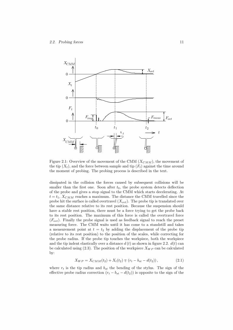
2.2. Probing forces 11
F
X
FF
X
X
X
X
F
CMM
CMM
t
t
t
imp ovt
ovt
meas
t1t0 t2t
0
0
0
Figure 2.1: Overview of the movement of the CMM (XCMM ), the movement ofthe tip (Xt), and the force between sample and tip (Ft) against the time aroundthe moment of probing. The probing process is described in the text.
dissipated in the collision the forces caused by subsequent collisions will besmaller than the first one. Soon after t0, the probe system detects deflectionof the probe and gives a stop signal to the CMM which starts decelerating. Att = t1, XCMM reaches a maximum. The distance the CMM travelled since theprobe hit the surface is called overtravel (Xovt). The probe tip is translated overthe same distance relative to its rest position. Because the suspension shouldhave a stable rest position, there must be a force trying to get the probe backto its rest position. The maximum of this force is called the overtravel force(Fovt). Finally the probe signal is used as feedback signal to reach the presetmeasuring force. The CMM waits until it has come to a standstill and takesa measurement point at t = t2 by adding the displacement of the probe tip(relative to its rest position) to the position of the scales, while correcting forthe probe radius. If the probe tip touches the workpiece, both the workpieceand the tip indent elastically over a distance d (t) as shown in figure 2.2. d(t) canbe calculated using (2.3). The position of the workpiece XWP can be calculatedby:
XWP = XCMM(t2) + Xt(t2)∓ (rt − bst − d(t2)) , (2.1)
where rt is the tip radius and bst the bending of the stylus. The sign of theeffective probe radius correction (rt − bst − d(t2)) is opposite to the sign of the

12 Chapter 2. Design considerations
d t
F t
probe tip
workpiece
t( )
( )
Figure 2.2: Indention d(t) of a sphere and a plane due to a force Ft(t).
probing speed4 . For the direction as plotted in figure 2.1 the sign is positive. rtand bst are most commonly determined by a probe system calibration. Whetheror not the software should correct for the indentation d (t2) , depends on thecircumstances. E.g. for an aluminum workpiece, a sapphire 0.3 mm diametertip, and a static probing force of 4.9 · 10−5 N, the indentation is 1 nm.
The forces exerted during the probing process are small, but often not smallenough to prevent damage of the workpiece, especially for soft materials likealuminum, copper, or brass. In the next paragraph the maximum force a work-piece can stand without plastic deformation is estimated. Then the impact andthe overtravel force are calculated and compared to the admissable force. It isassumed that the probe has stopped bouncing before the CMM reaches its over-travel, so that the impact and overtravel force occur at different times. Whetherthis is true, depends on the time between the first collision and the maximumovertravel (t1 − t0), the natural frequency of the probe and its suspension, andthe speed with which the kinetic energy of the probe system’s suspended massis dissipated. We shall see that the natural frequency is typically above 500 Hz.As an example, the probe’s deflection is calculated assuming a 5% energy lossper collision, a probing speed of 1 mm s−1, a CMM deceleration of 100 mm s−2
starting immediately after the first contact of the probe with the workpiece,and a natural frequency of 500 Hz. The result is plotted in figure 2.3. Since thecollision speed attenuates to 5% in less than half of the time the CMM needsto come to a standstill, it is safe to regard impact forces and overtravel forcesseparately.
4Less generally, this can be stated as: When measuring a cylindrical hole, this implies thattwo times the effective probe radius should be added to the CMM measurement. In case ofan external measurement (e.g. a rod) two times this radius should be subtracted form theCMM measurement.

2.2. Probing forces 13
0 5 10 15-5
-4.5
-4
-3.5
-3
-2.5
-2
-1.5
-1
-0.5
0probe bouncing
time in ms
prob
e de
flec
tion
X i
n µm
Figure 2.3: Theoretical analysis of the probe bouncing. After 4.8 µs the colli-sion speed is decreased to 5% of its original value. Model parameters: naturalfrequency 500 Hz, probing speed 1 mm s−1, CMM deceleration 100 mm s−2, 5%energy dissipation per collision.
2.2.2 Admissable probing force
In this paragraph the admissable probing force FY is calculated. FY is definedas the probing force for which the shear stress at a point somewhat beneaththe surface exceeds a critical value and plastic deformation starts. This value isdetermined by the elastic limit of the workpiece. Usually the yield strength σYof a material is specified instead of the elastic limit5 . As the numbers differ by afew percent only, they can be interchanged for the description of the admissableprobing force. To prevent plastic deformation, Ft should always be smaller thanFY .
Because the onset of plastic deformation lies somewhat beneath the surface,potential damage of the surface is hard to detect. Some authors debate thereforethat the constraint might be too tight [Vliet 96]. Van Vliet proposes anothercriterium based on hardness numbers, which leads to an approximately twice ashigh admissable force. Residual stresses, however, caused by plastic deformationbeneath the surface, might cause subtle changes of the surface which can affectthe optical properties of the workpiece. This can not be accepted when theworkpiece is an optical part like a lens or a mirror. In this thesis therefore a
5 In the rare case that the yield strength of the workpiece is higher than the yield strengthof the probe tip, plastic deformation will occur first in the probe tip. σY then denotes theyield strength of the probe tip.

14 Chapter 2. Design considerations
safer admissable force based on the onset of plastic deformation is chosen. Thisforce can be calculated as [Vliet 96]:
FY ≈ 85r2t σ
3Y
E2r
(2.2)
1
Er=
1
2
((1− ν21
)E1
+
(1− ν22
)E2
)
where Ei, νi are the Young’s modulus and the Poisson ratio respectively with ilabeling the probe tip (1) and the workpiece (2), and where rt is the radius ofthe probe tip. Er is called reduced Young’s modulus. The workpiece is assumedto be flat.
2.2.3 Impact force
The collision of the probe with the workpiece can be modelled as a sphere withmass m∗ colliding to a flat surface. m∗ is here the equivalent mass of the probeand everything that is stiffly connected to it, i.e. the mass that is felt whentrying to accelerate the probe tip. The calculation of the impact force is basedon Hertz’s theory which describes the summed indentation of two sphericalbodies pressed together by a certain force. In our case, the summed indentationd(t) of the probe tip (radius rt) and the workpiece (sphere radius ∞) can beexpressed as function of the probing force Ft(t), as [Dubbel 81]:
d(t) = 3
√9F 2
t (t)
4rtE2r
. (2.3)
where rt is the probe tip radius and where the workpiece is assumed to be flat,i.e. having an infinite radius.
Using (2.3) the force of a spherical body colliding to a plane can be calculatedby solving the differential equation
Ft(t) =2
3
√rtEr d(t) 32 = m∗d(t) (2.4)
Szabo solved equation (2.4) and found for the impact force Fimp (defined as themaximum of Ft) [Szabo 77]:
Fimp =5
√125
9m∗3v60E
2rrt, (2.5)

2.2. Probing forces 15
where v0 is the speed of the CMM at the moment of probing. The admissableimpact speed vimp is defined as the probing speed for which Fimp equals FY . Itcan be calculated by combining equations (2.5) and (2.2):
vimp = 41
√r3t σ
5Y
E4rm
∗. (2.6)
From equation (2.6) it is clear that the maximum impact speed depends onmaterial properties (E, ν, and σY ) of both the workpiece as the probe tip, theradius of the probe tip, and the equivalent mass of the probe. The workpiecematerial is given and is surely not a design parameter. The probe tip material isnormally a very hard material like ruby or hardened steel to prevent excessivewear of the tip. The tip radius is mostly determined by the measurementproblem: to measure a small hole for example a small tip radius is necessary.The only real design parameter is the equivalent massm∗ of the probe. It shouldbe kept as low as possible. For a material like aluminum, frequently used forprecision products, probed with a 0.3 mm diameter ruby tip and requiring aprobing speed of about 1 mm s−1 the reduced mass should be no more thantwenty milligram, as can be seen in figure 2.4.
Overtravel force
Each CMM will move on over a certain distance, the overtravel Xovt, after astop signal is given by the probe system. The probe is then moved from its
0.2 0.3 0.4 0.5 0.6 0.7 0.8 0.9 110-1
100
101
102
probe tip diameter in mm
adm
issa
ble
im
pact
spee
d in m
m/s
admissable impact speed
Al , 5mg Al , 10mgAl , 20mg
st , 5mg st , 10mg st , 20mg
Figure 2.4: Admissable impact speed as function of the probe tip radius for aruby tip (E=480 kN/mm2). As workpiece material steel (E = 20 ·104 N mm−2,σY = 800 N mm−2) and an aluminum alloy (E = 7 · 104 N mm−2, σY =280 N mm−2) are taken. The equivalent mass of the probe is given at the righthand side of the plot. Equation (2.6) is used to generate this plot.

16 Chapter 2. Design considerations
rest position and the suspension will try to move it back to its rest positionby exerting a counter force, like explained in figure 2.1. It is assumed for themoment that the counter force is linear with the translation of the tip andthat the direction of the force is parallel to the translation of the tip. Thismeans that a stiffness ct can be defined as the quotient of the force and thetranslation. These assumptions will be checked after the suspension has beendeveloped. The maximum of the counter force is called the overtravel force Fovt.It can be calculated to be:
Fovt = ctXovt (2.7)
The overtravel mainly depends on the dynamics of the CMM and the probingspeed. However, some estimate of the overtravel that can occur is necessarybecause this sets an upper limit for the stiffness of the suspension. Becausethe electronics in the probe system and the CMM need time to react, it is notreasonable to assume that the CMM can start decelerating immediately afterfirst contact between the probe and the workpiece. Therefore a reaction time tris introduced. Further it is assumed that the CMM starts decelerating at t =t0 + tr with a constant negative acceleration aCMM . It is then straightforwardto calculate the overtravel Xovt as:
Xovt = v0tr +v20
2aCMM
(2.8)
Combining equations (2.2), (2.7), and (2.8), an expression for the overtravelspeed vovt, i.e. the admissable speed regarding overtravel, can be found:
vovt = −traCMM +
√(t2ra
2CMM + 170
r2tσ3Y
ctE2r
aCMM
)(2.9)
Equation (2.9) is plotted in figure 2.5 for a reasonable 2 ms reaction time anda CMM deceleration of 0.1 m s−2, being the design parameter for the high ac-curacy CMM that was developed by Vermeulen [Vermeulen 95]. From the plotcan be seen that the stiffness of the suspension should be smaller than about200 N m−1 in order to enable probing with a probing speed of 1 mm s−1 and a0.3 mm diameter ruby tip.
After this analysis the implicit requirement ‘the workpiece may not be damagedby the probing’ may be replaced by two explicit ones:
• The equivalent mass should be smaller than 20 mg.
• The stiffness of the suspension should be smaller than 200 N m−1.
These requirements are used in the next section to develop the suspension.

2.3. Suspension 17
0.2 0.3 0.4 0.5 0.6 0.7 0.8 0.9 110
-1
100
101
102
probe tip diameter in mm
adm
issab
le o
vertr
avel
spee
d in
mm
/s
admissable overtravel speed
Al , 50N/m
Al , 100N/m
Al , 200N/m
st , 50N/m
st , 100N/mst , 200N/m
Figure 2.5: Admissable overtravel speed for a ruby probe tip as function of thetip diameter as given by equation (2.9). The stiffness of the probe suspensionand the workpiece material are indicated on the right side. The tip and work-piece materials characteristics are equal to the materials mentioned in figure2.4.
2.3 Suspension
In this section the suspension of the probe system is developed. The main task ofthe suspension is to give the probe a stable rest position and orientation relativeto the probe house while enabling moving of the probe tip(s) in three orthogonaldirections in order to enable overtravel of the CMM. Several requirements canbe formulated:
1. The mass needed for the suspension which moves together with the probeshould be small in order to keep the equivalent mass of the probe below20 mg, as explained in the previous section.
2. The suspension preferably fixes all Degrees Of Freedom (DOF’s) of theprobe which are not necessary for the movement of the probe tip in threeorthogonal directions. Here fixation means that the translation of theprobe tip, caused by the translation or rotation of the probe in the fixeddirection, is either substantially smaller than the intended probe uncer-tainty, or can be predicted from the measured probe position substantiallybetter than the probe uncertainty. Each DOF of the probe should bemeasured by the measuring system adding extra complexity to the probesystem.
3. The probing force due to displacement of the tip from its rest position

18 Chapter 2. Design considerations
should be small enough not to damage the workpiece. In case the staticprobing force is linear to the tip displacement a tip stiffness can be definedwhich should be smaller than 200 N m−1, as is shown in the previoussection.
4. The maximum overtravel the suspension can resist should be as high aspossible, preferably as high as the overtravel in case of a emergency stopat maximum speed. For a maximum speed of 10 mm s−1, a decelerationof the CMM of 0.1 m s−2, and a reaction time of 2 ms, the maximumovertravel is about 0.5 mm as calculated in (2.8).
5. It should be possible to deduce the (static) probing force from the tipposition with a reproducibility of at most a few percent.
6. The suspension should fit in a probe house as described in requirement 4in the introduction. Especially the width of the suspension should be lessthan twice the stylus length. The height depends on the available spacein the CMM, but is probably less crucial.
7. The natural frequency of the probe should be high, preferably a few hun-dred Hertz. This attenuates the free oscillation of the probe. Oscillationenergy built up during moving to the next measuring point will be dissi-pated in the probing process causing a higher impact force. Besides, probeoscillation also hinders the first detection of a surface which will increasethe reaction time. Finally, a high natural frequency will attenuate thebouncing quickly. This will assure that the bouncing has stopped beforethe CMM reaches its overtravel.
The suspension can be based on a number of different guiding systems likeelastic hinges, rolling bearings, magnetic bearings, and air bearings. Giventhe small moving range (about 0.5 mm), the required unique rest position andthe very limited mass that can be used (20 mg), elastic hinges are the logicalchoice. Rolling bearings have problems in restricting the fixed directions withsufficiently low uncertainty, violating requirement 2. Magnetic bearings requirethe use of active elements with accompanying measurement and control systems.3D air bearings are unattractive because a preloading mechanism is required andbecause no light construction could be found which fixes the appropriate DOF’s.Therefore only elastic hinges are considered in the rest of this section.
Consider a simple probe consisting of a stylus with a single spherical tip con-nected to a suspension. Define an orthogonal axis system with the z-axis alignedalong the stylus and the origin at the end of the stylus which is connected tothe suspension. To enable movement of the tip in x-, y-, and z-direction whilefulfilling requirement 2 the suspension should enable only:
• translation in z-direction (Tz)• either translation in x-direction (Tx) or rotation along the y-axis (Ry)

2.3. Suspension 19
Figure 2.6: The probe tip (T) and the stylus (S) are suspended to the probehouse by three slender rods (R) tangentially touching an intermediate body (I).The free ends of the rods are to be connected to the probe house.
• either translation in y-direction (Ty) or rotation along the x-axis (Rx),
which makes four principle options for the suspension. Note that rotation alongthe z-axis (Rz) is fixed in all options. From these alternatives only the sus-pension enabling Tz, Ry, and Rx can be made in a single stage, i.e. withoutusing extra intermediate bodies [Schellekens 98]. The other options can only berealised in multi stage suspensions. A well known example of the latter is theanalogue probe made by Zeiss (see chapter 1 figure 1.4). Its suspension basicallyconsists of three stacked parallel leaf spring guideways connected to each otherby intermediate bodies. Because the mass of the suspension together with themass of the probe and the moving mass of the measurement system should beas small as possible (but in any case smaller than 20 mg), it is undesirable touse a suspension with more than one intermediate body. Three possible singlestage suspensions are considered:
1. The probe is connected to an intermediate body which is suspended to theprobe house by three slender rods6 tangentially touching the intermediatebody (figure 2.6). It is essential that the rods do not touch radially, asthe intermediate body would then be both underdetermined (Rz) andoverdetermined (Tx or Ty).
6A slender rod is defined as an elastic element whose length is much larger than the widthand the thickness. Because its stiffness in the length direction is at least an order of magnitudehigher than the stiffness in other directions, it can be seen as an element which fixes one DOF.Due to its finite length, sideways displacements result in a parasitic motion in the constraineddirection. The same function is performed without this disadvantage by a folded leaf spring[Schellekens 98].

20 Chapter 2. Design considerations
x
y z
L
Figure 2.7: The probe is suspended to the probe house by a leaf spring (L). Theopposite end of the leaf spring is to be connected to the probe house.
Figure 2.8: The probe is suspended to the probe house by a membrane (M).The outer side of the membrane is to be connected to the probe house.
2. The probe is connected to an intermediate body which is suspended tothe probe house by a leaf spring (figure 2.7).
3. The probe is connected to an intermediate body which is suspended tothe probe house by a flat membrane (figure 2.8).
For each of the suspensions a stiffness matrix C can be defined, which transfersa probe tip deflection to a probing force:
Ft =C Xt (2.10)

2.3. Suspension 21
Suspension 1 has a diagonal stiffness matrix in the frame as indicated in figure2.6, as is explained in appendix A (equation (A.11)). The diagonal elements forthe x- and y-directions are equal. This implies that the probing force is parallelto the tip deflection if the deflection is in the xy-plane or in the z-direction.The sensed stiffness is equal for all deflections in the xy-plane. The absolutestiffness in one direction, e.g. the z-direction can be chosen at will, dependingon the geometry of the slender rods, but for all stiffnesses to be equal, thestylus should be relatively short. Due to the suspension’s cylindrical symmetry,the thermal center is at the z-axis. Due to parasitic translation in the lengthdirection of the rods when they are translated out of the xy-plane, the probewill show rotation around the z-axis when moved in vertical direction. Thisrotation can be calculated from the measured translation in z-direction so thatsoftware error compensation can be used. In case the tip is not at the z-axis, itwill move over a small distance in x- or y- direction when moved in z-direction.
The sensed stiffness at the probe tip of suspension 2 can be calculated usingequation (A.1) in appendix A, where Cs1 is the 6D stiffness matrix transform-ing displacements and rotations of the free end of a leaf spring to forces andmoments. Suppose a force Ft (Ft,x, Ft,y, Ft,z) is applied to the tip. This force
causes a force F and a moment M at the end of the leaf spring connected tothe intermediate body. F and M can be transformed to displacements Xl androtations Rl of the free end of the leaf spring, using the inverse stiffness matrixC−1s1. Knowing Xl and Rl, the probe tip displacements can be calculated. Using
that the thickness (ts) of a leaf spring is small compared to its length (ls) and
its width (ws), the relation between Ft and Xt can be expressed as:
Ft = C2 Xt (2.11)
C2 =Est
3sws
lsl2st
1
6 (1 + νs)0 0
01
3− lst
2ls
0 − lst2ls
l2stl2s
,
where Es and νs are the Young’s and Poisson modulus of the leaf spring ma-terial, and where lst is the stylus length. The 3D stiffness matrix can be diag-onalised by displacing the stylus so that the tip is under the centre of the leafspring. C′
2 then becomes:
C ′
2 =Est
3sws
lsl2st
1
6 (1 + νs)0 0
01
120
0 0l2stl2s
. (2.12)
By changing the dimensions of the leaf spring, the absolute value of the stiff-ness for the x-, y-, and z-direction can be set together. The mutual ratios of the

22 Chapter 2. Design considerations
stiffness in the different directions can not be chosen freely. The stiffness in thex- and y-direction have a fixed ratio of about 0.65, depending on the Poissonratio only. The stiffness in the z-direction can be made equal to the stiffnessin x- or y-direction, but this requires a relatively short stylus. The three diag-onal elements being different from each other implies that the probing force isonly parallel to the probing direction if probing in purely x-, y-, or z-direction.Suspension 2 has no cylindrical symmetry and hence the thermal center is notat the z-axis. In case the stylus is displaced to the centre of the leaf springby an intermediate body, and the intermediate body material has the samethermal expansion coefficient as the leaf spring material, this suspension has athermal centre at the symmetry axis of the stylus. The difference in thicknessof the intermediate body and the leaf spring, however, will make the suspensionsensitive to temperature variations.
Suspensions 3 is overdetermined which can cause internal stresses which makethe prediction of mechanical and thermal behavior difficult. Consequently thelength of the membrane has to increase when moved in z-direction. This willlead to a non constant stiffness in z-direction. A non flat membrane does notsuffer from this overdetermination, but since it does not fix Tx and Ty, it is notregarded here. Due to symmetry, the thermal center is at the z-axis.
The third suspension is rejected because of the overdetermined Tx and Ty.Suspension 1 has greater symmetry and equal diagonal elements for the x- andy-direction. It was therefore preferred above suspension 2. Suspension 1 isstudied more extensively in appendix A, and used as suspension for the probesystems described in this thesis.
2.4 The measurement system
Now we have chosen the suspension, it is known that the probe has in goodapproximation Tz, Rx, and Ry degrees of freedom.7 The measuring systemshould be able to measure all these DOF’s. The following requirements shouldbe met:
1. The 3D uncertainty, converted to tip coordinates, should be smaller than20 nm. If necessary the probe system can be calibrated against the scalesof the CMM before each measurement sequence. Therefore a short term(one hour) stability satisfies. The required uncertainty for Tz is 20 nm.The required uncertainty for Rx and Ry depends on the probe length. Fora 10 mm stylus length, for example, the Rx and Ry uncertainty should besmaller than 2 µrad.
2. The interaction force of the measuring system with the probe should besmall, i.e. substantially smaller than the measuring force (Fmeas in figure
7 In appendix A equation (A.10), it is calculated that the tip displacement due to puretranslation is at least a hundred times smaller than the pseudo-translation due to rotation.

2.4. The measurement system 23
2.1). It is not known at this stage what the optimal measuring force willbe. Therefore the measuring system should preferably be contactless. Ifthe measurement system is not contactless, it is still possible that theinteraction force can be accepted. Which force can be tolerated dependson the characteristics of the force. If it is proportional to the displacementof the probe, it adds to the stiffness of the suspension. It should bechecked whether the combined stiffness does not exceed the required limitof 200 N m−1. If the force of the measurement system acts like a frictionforce, it will induce virtual backlash, which must be incorporated in theerror budget.
3. A measuring range equal to the range of the suspension is preferred. Itenables measurements at large deflections of the probe and facilitates thecontrolling of the CMM to achieve the desired measuring force. However,in many cases measurements will be performed at small deflections tolimit the counter force of the suspension. Therefore a measuring range(converted to probe tip displacements) of 10 µm can be accepted. Outsidethis range, an indication on which side the probe is out of range is neededas feedback signal for the CMM.
4. The stand off distance of the measuring system relative to the probe shouldbe large enough to enable full 0.5 mm swing of the probe in any direction(as stated in requirement 4 for the suspension). However, the measure-ment system is allowed to be out of range, as discussed above.
5. The measuring system should not obstruct the approachability of theprobe, as stated in requirement 4 in the introduction.
6. The mass of the moving part of the measuring system and the suspensionadded to the probe mass should be smaller than 20 mg.
Four measurement systems have been considered: optical sensors, capacitivesensors, strain gauges, and inductive sensors. All these systems are describedin the remainder of this section.
2.4.1 Optical sensors
To measure the angle of the probe (i.e. Rx and Ry) optically it is necessary toattach a mirror to the probe. The mass of this mirror adds to the equivalentmass so the mirror should be as light as possible. A triangulation setup is usedto measure the tilt of the mirror, like indicated in figure 2.9.
A beam coming from a collimated light source reflects at the mirror and falls ona sensor which detects the 2D position of the spot on its surface. This sensorcan be a 2D lateral effect photo diode (also called position sensing detector,
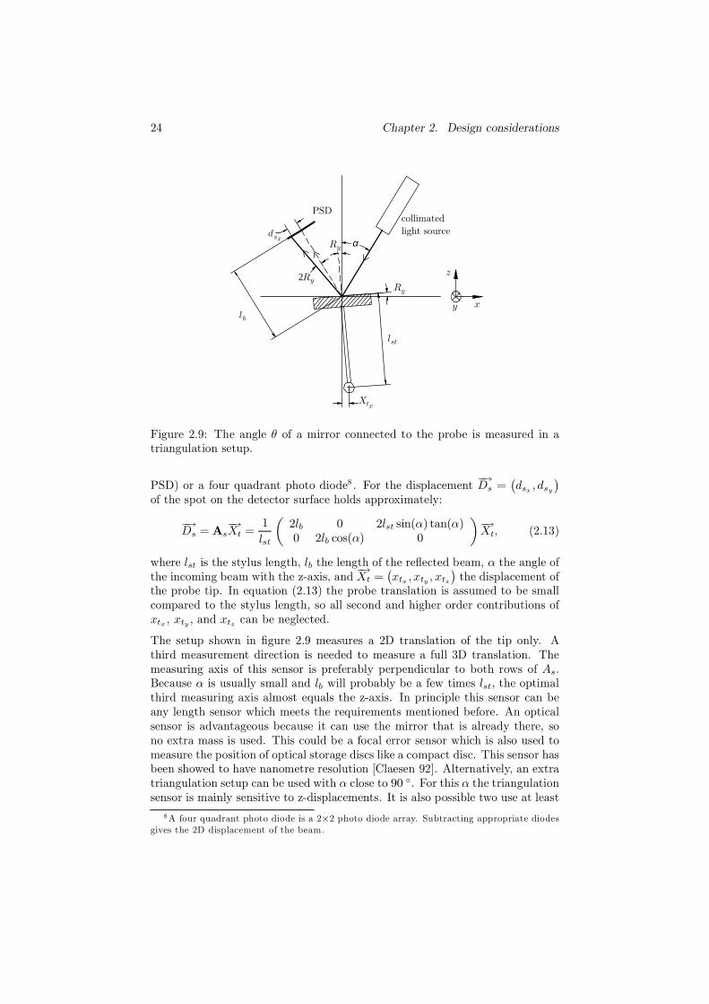
24 Chapter 2. Design considerations
dsx α
2
lst
X
R
R
R
t
y
y
y
x
lb
z
y x
collimated
light source
PSD
Figure 2.9: The angle θ of a mirror connected to the probe is measured in atriangulation setup.
PSD) or a four quadrant photo diode8 . For the displacement−→Ds =
(dsx , dsy
)of the spot on the detector surface holds approximately:
−→Ds =As
−→Xt =
1
lst
(2lb 0 2lst sin(α) tan(α)0 2lb cos(α) 0
)−→Xt, (2.13)
where lst is the stylus length, lb the length of the reflected beam, α the angle ofthe incoming beam with the z-axis, and
−→Xt =
(xtx , xty , xtz
)the displacement of
the probe tip. In equation (2.13) the probe translation is assumed to be smallcompared to the stylus length, so all second and higher order contributions ofxtx , xty , and xtz can be neglected.
The setup shown in figure 2.9 measures a 2D translation of the tip only. Athird measurement direction is needed to measure a full 3D translation. Themeasuring axis of this sensor is preferably perpendicular to both rows of As.Because α is usually small and lb will probably be a few times lst, the optimalthird measuring axis almost equals the z-axis. In principle this sensor can beany length sensor which meets the requirements mentioned before. An opticalsensor is advantageous because it can use the mirror that is already there, sono extra mass is used. This could be a focal error sensor which is also used tomeasure the position of optical storage discs like a compact disc. This sensor hasbeen showed to have nanometre resolution [Claesen 92]. Alternatively, an extratriangulation setup can be used with α close to 90 . For this α the triangulationsensor is mainly sensitive to z-displacements. It is also possible two use at least
8A four quadrant photo diode is a 2×2 photo diode array. Subtracting appropriate diodesgives the 2D displacement of the beam.

2.4. The measurement system 25
two triangulation sensors with moderate α to measure all DOF’s. Van Vlietused this approach to construct his probe system [Vliet 96].
2.4.2 Capacitive sensors, strain gauges, and inductive sen-
sors
The probe tip translation can also be measured by three or more 1D displace-ments sensors at distinct points. These points should be as far away from theaxis of rotation as allowed by the requirements. The most logical choice is thepoints where the rods are connected to the intermediate body because otherwiseextra mass needs to be added. The sensors are best divided over 120 , like in-dicated in figure 2.10. In this case the three sensors measure the z-displacementof the intermediate body at their positions. The uncertainty needed for thesensors depends on a ratio q defined as:
q =rslst, (2.14)
where rs is the distance of a measuring point to the rotation point and lst isthe stylus length. A matrix A can be defined which describes the translationsmeasured by the sensors, gathered in a vector
−→M , when the probe tip is moved
over a distance−→Xt:
−→M =A
−→Xt (2.15)
rsz x
y
M
M
M
1
3
2
Figure 2.10: Three sensors (M1 ... M3) measure the z-position of the interme-diate body at the marked positions

26 Chapter 2. Design considerations
Using the geometry given in figure 2.10 and equation (2.14), A can be calculatedto be:
A =
q 0 1− 12q 1
2
√3q 1
− 12 q − 1
2
√3q 1
. (2.16)
From (2.15) and (2.16) it can be seen that the measuring system is in generalmore sensitive in some directions than in others. It is shown in appendix Aequation (A.43) that the resolution resmin in the least sensitive direction is:
resmin =resms3
, (2.17)
where resm is the resolution of the used sensor and s3 is the smallest singularvalue of A. The singular values of A can be calculated to be:
svd (A) =
(√3,
1
2
√6q,
1
2
√6q
). (2.18)
Because the probe system may not be more than twice as wide as the styluslength (requirement 5), q is necessarily smaller than 1. The smallest singularvalue of A is therefore 1
2
√6q, so the worst case resolution can be written as:
resmin =1
3
√6resm
q. (2.19)
For a reasonable value q = 0.5 it follows that the resolution of each individualsensor should be about 12 nm to reach an overall resolution of 20 nm. Sensorsthat have been considered are:
• capacitive sensors,• piezo-resistive strain gauges on the slender rods,• inductive sensors.
These sensors will be discussed below.
Capacitive sensors Capacitive sensors are known to have impressing res-olutions down to the nanometre level or even below. The main problem forapplication of these sensors in the probe system is that they require either largeplates or small distance between the plates to get reasonable nominal capaci-tance values (usually between 0.1 and 10 pF). To estimate the applicability ofcapacitive sensors, a design where all available space is filled with three sen-sors is studied. Consider the configuration drawn in figure 2.11, where threecapacitor plates are divided equally over a circle which is not bigger than theouter point of the rods. The plates are oriented horizontally and form three

2.4. The measurement system 27
Figure 2.11: Capacitive measuring system: The condensor plates C1 to C3 are tobe connected to the ends of the intermediate body. They measure the distanceto a ground plane slightly above (not drawn).
capacitors with three fixed electrically grounded plates above the drawn plates.The capacitances of the three capacitors can be used to calculate the positionof the probe tip. With a plate separation d of 0.5 mm the nominal capacitanceis
C ≈ ε0εr13πr2c
d≈ 0.5 pF, (2.20)
where 5 mm is taken for the radius rc of the sensors. Because capacitive sensorstake an average over their surface, the ratio q is reduced by a factor 0.55. So witha stylus length of 10 mm and a capacitor plate radius of 5 mm q equals 0.275.Therefore an uncertainty of ∆d = 6.7 nm is needed for an overall uncertaintyof 20 nm. This means that a capacitance change ∆C of
∆C =∂C
∂d∆d = −ε0εr
13πr2c
d2∆d ≈ −6.2 · 10−18 F (2.21)
should be measured, which is impossible with reasonable effort. Therefore thecapacitance should be increased, probably by giving up part of the overtravel.Suppose the plate distance is reduced to 0.1 mm, then the capacitance changeto be measured increases to 1.5 · 10−16 F at a nominal capacitance of 2.3 pF,which should be possible to detect [Zhu 92].
In equation (2.20) the electrical field between the plates is assumed to be uniformand the edge effects are neglected. In reality the edge effects will be present andwill cause deviations from (2.20) and cross-talk between the sensors. Further-more, the plates are assumed to be parallel to each other, which is definitely notthe case, given the Rx, Ry, and Tz DOF’s of the suspension. A model describingthese effects must be made if these sensors are used in the probe system. Thedeviations can be partly prevented by using a so called guard which surrounds
28 Chapter 2. Design considerations
the moving plate of the sensor at equal potential. This, however, will reducethe effective area of the sensor which reduces the resolution. It is thereforeundesirable. A third plate at the other side of the moving plate (the movingplate is then sandwiched between two fixed plates) can be used to linearise therelationship between displacement and capacitance change. Extra space at thebottom side of the probe system is required which reduces the effective probelength, but it might be advantageous anyway.
The moving plates of the capacitive sensors will add extra mass to the probe,which will increase the impact force. Very thin metal foil is therefore to be used.E.g. a 10 µm steel foil with a radius of 5 mm has a mass of 6 mg. In principleit is possible to increase the resolution by stacking more than one moving plateper sensor above each other. However, the total mass of the probe, intermediatebody, and capacitive sensor will very soon exceed 20 mg.
Both Peggs et al. and Lu designed a probe system using capacitive distancesensors as measurement system [Peggs 99], [Lu 99]. Both used the same sus-pension as proposed in this thesis and also in earlier publications [Haitjema 01],[Pril 97], [Pril 95]. Peggs et al. estimated a resolution of 3 nm. They optfor equal stiffness in all directions, which makes their stylus necessarily shortcompared to the width of the suspension. The working range is 20 µm. Thesuspended mass is 360 mg. In combination with a 1 mm diameter sphericaltip and a stiffness of 10 N m−1, the impact and overtravel force are acceptable.The resulting natural frequency is 26 Hz,which will cause a rather long bouncingtime.
Lu fills all available space in the plain of the rods with four capacitor plates.He sandwiched the four moving plates between a top and a bottom fixed plate,which makes the relation between translation and capacity of the sensors morelinear. He analysed the effect of tilts on the capacity. The probe system hasnot (yet) been realised. The predicted uncertainty is 10 nm.
Piezo-resistive strain gauges
If the probe tip is moved from its rest position the slender rods will be deflectedfrom their equilibrium, so strains are present at their surfaces. These strainscan be measured by strain gauges. The tip displacement can be calculated fromthe measured strain. This way it is possible to have a measuring system whichneeds no additional space and adds virtually no mass.
Strain gauges can detect the relative strain ε in a material because their resis-tance R changes as function of ε according to [Middelhoek 89]
∆R
R= Gε, (2.22)
where G is called the gauge factor. G is a scalar for isotropic materials or afourth rank tensor otherwise. The resistance change is caused by two effects:

2.4. The measurement system 29
• change of geometry: This can be compared to stretching a wire: the wirebecomes longer and thinner, which increases the resistance. This effect ispresent in all materials, but is rather small. G varies between 1.6 and 2,depending on the Poisson ratio.
• change of the specific resistance: The specific resistance of certain mate-rials, e.g. silicon, depends on the strain. This is called the piezo-resistiveeffect. Physical description of this effect requires knowledge on the bandstructure of the crystals involved, which falls outside of the scope of thisthesis. More information can be found in Middelhoek [Middelhoek 89].This effect can be much larger than the geometrical effect. For crystallinesilicon a gauge factor of 173 is possible, depending on doping, crystal di-rection, and temperature. For polycrystalline or amorphous silicon thegauge factor is about 30. Strain gauges mainly based on this effect arecalled piezo-resistive strain gauges.
Usually strain gauges are connected to the stressed surface by glueing, whichmay cause hysteresis, resulting in increased uncertainty. By using several evap-oration, lithography and etching steps the slender rods, the strain gauges, andtheir electrical connections can manufactured in one setup. This technologybelongs to the field of Micro System Technology (MST). It enabled integratedfabrication of mechanics, sensors, actuators, and electronics on a micrometrescale. As a spin-off of integrated circuit technology silicon is mostly used asa substrate. Products made by MST are also called Micro Electro MechanicalSystems (MEMS).
To estimate the applicability of strain gauges, the strain in the rods has to becalculated. An approximated calculation is performed below. A more thoroughanalysis is described in appendix A which leads to the result expressed in (A.38).Imagine a rod whose free end is moved downwards by a force F while the endis kept horizontally9 , like is shown in figure 2.12. For this a moment M0 isnecessary. The moment M at any position can be calculated to be (usingstandard elastic theory):
M = Fx−M0 (2.23)
M0 = 12 lsF,
where ls is the length of the rod and x a parameter labeling a position on therod in the length direction (0 x ls). The stress in length direction (usuallydenoted as σxx) can be calculated by dividing M by the moment of bendingresistance Wb:
σxx =M
Wb
=6(12 lsF − xF
)wst2s
(2.24)
9Here the rotation of the rod is neglected. As the probe has freedom of motion for rotationaround a horizontal axis this assumption is not met in praxis. In appendix A a more accuratecalculation is given. The error made due to this approximation depends on the geometry ofthe probe system, but is typically 30%.

30 Chapter 2. Design considerations
ls
y
R R2 3,
R R1 4,
x
z
xz
F
M
1R
4R3R
2R
M0
M0
M 0
0
A
B
D
CV 0
Vm
1R 2R
3R4R
top view
side view
moment
Wheatstone bridge
Figure 2.12: Strain gauges on a rod in a top and a side view. The moment inthe rod in the shown position is indicated. The change of the resistance of thestrain gauges is measured in a Wheatstone bridge configuration.
where ws and ts are the width and the thickness of the rods. The strain is foundby dividing σxx by the Young’s modulus Es of the rod material:
εxx =σxxEs
=3F
Eswst2s(ls − 2x) . (2.25)
The strain gauges are best placed at positions of maximum and minimal strain,i.e. at x = 0 and x = ls. Furthermore, F in (2.25) can be replaced by thedisplacement in z-direction z, using the already calculated stiffness in z-directionof a rod cs,zz (equation (A.2)). The strain at the position of the strain gaugescan then be expressed as:
cszz =Est
3sws
l3s(2.26)
εsg = ± 3lsF
Eswst2s= ±3lscs,zzz
Eswst2s=±3
tsl2s
z (2.27)
Here the positive answer applies for x = 0 and the negative for x = ls. Assumingpoly silicon strain gauges (G = 30) and reasonable values for ts (20 µm) and ls(1.6 mm) it can be calculated using (2.22) and (2.27) that the relative resistancechange caused by a rod displacement of 12 nm is
∆R
R≈ ±8 · 10−6. (2.28)
The change of resistance of the strain gauges can best be detected in a Wheat-stone bridge configuration where all four resistors are strain gauges. Besides

2.4. The measurement system 31
highest sensitivity this has the advantage that temperature effects are partlycompensated. When temperature effects are taken into account equation (2.22)changes to [Middelhoek 89]:
∆R
R= αT + G′ (1 + βT ) ε (2.29)
G′ =G
1 + 293.15β
where α and β are constants. The output voltage Vm of the Wheatstone bridgecan be approximated by:
VmV0
=∆R1 −∆R2 −∆R3 + ∆R4
4R(2.30)
Combining (2.29) and (2.30), and assuming a homogeneous temperature dis-tribution over the slender rod, it can be seen that the effect of αT on Vm/V0cancels while the effect of βT leads to a relative error. The values of α andβ highly depend on processing parameters and the doping of the poly silicon.If necessary Vm/V0 can be software corrected for temperature. A temperaturesensor close to the strain gauges should therefore be included.
An advantage of the use of strain gauges is that virtually no extra mass isattached to the probe, so that the impact force is kept as low as possible. Thestrain gauges do not require any extra space which is another advantage. Theproduction cost of this system are rather low for large batches, but are highfor a single piece or small series. Silicon is a brittle material which makes thestructure sensitive to shock load. Special care has to be taken during assembling.Apart from this, the assembling is relatively easy. The overtravel reachable withsilicon rods depends on the yield strength of silicon. In principle this is as highas 7000kN mm−2, which is much higher than the strongest steel. In practicethe effective yield strength is reduced depending on crystallographic orientation,the number and size of surface, edge, and bulk imperfections, and the stressesaccumulated during growth, polishing, and subsequent processing [Petersen 82].In principle other substrate materials can be used. Due to the large experiencegained with the deposition of strain gauges on silicon, other materials have notbeen considered in this research. It might however be interesting to see in afollow up research if it is possible to use alternative substrates, like high yieldstrength metals, which are less sensitive to shock loads.
Inductive sensors
Different types of inductive sensors exist. The most accurate are the so calledLVDT’s (Linear Variable Differential Transducers) where a core is moving ina set of coils. Wetzels showed that they can reach subnanometre resolutionand few nanometre uncertainty [Wetzels 98]. Other inductive sensors directlymeasure the distance to a conductive counter part, but they lack the required
32 Chapter 2. Design considerations
accuracy and are not regarded here [Schoot 98]. The core of an LVDT shouldmake a neat one dimensional translation, so it can not be connected directlyto the intermediate body. A straight guiding mechanism is necessary for eachLVDT. Care should be taken not to add to much stiffness to the intermediatebody because otherwise the overtravel force gets too high. To prevent overde-termination the core should be decoupled from the intermediate body in alldirections but the z-direction. These provisions will make the probe systemrather complicated. Besides this, considerable mass will be added to the probe.It is even questionable if it is possible to make the described mechanisms andthe cores of the LVDT’s using less than 20 mg.
2.4.3 Choice of measuring system
The choice for the measuring system to be used in the probe systems describedin this thesis is partly historical. The measuring system with strain gauges isvery attractive because no space is needed and no extra mass is added. How-ever, the costs for making the first prototype were out of budget, which madeit irrealistic at first. So at that time an optical measuring system was chosenbeing the second best solution. An optical prototype measuring translation in z-direction and one rotation has been designed in an early stage, and is describedin the next chapter. The capacitive and the inductive measuring systems wereless favourable because of the reduced overtravel capability and the relativelarge mass respectively. Later on, Mitutoyo Corporation, the Dutch Technol-ogy Foundation STW, and the Nederlands Meetinstituut (Dutch MeasurementInstitute, NMi), where found willing to contribute, which enabled the design andfabrication of a probe system with a silicon suspension and piezo-resistive straingauges as measurement system. This probe system is described in chapter 4.

Chapter 3
Design of a 2D optical
probing system
In this chapter the design of a 2D optical prototype is described. It is basedon a so called Laser Diode Grating Unit (more commonly known as LDGU)which was designed for use in CD players. The choice for the parameters of thesuspension and the probe is described, based on the principles which are alreadyexplained in the previous chapter. New preamplifier electronics are designed forlow noise and low power dissipation. This is described in section four. Finallythe design of the probe house is discussed.
3.1 The Laser Diode Grating Unit (LDGU)
The Laser Diode Grating Unit (LDGU) was designed for use in CD players whereit fulfills a threefold task: it generates two feedback signals to focus the laserspot on the disk and to follow the track, and it retrieves the digital data form thedisk. The use of the LDGU in CD players is described extensively in a book byBouwhuis et al. [Bouwhuis 85]. Technical data can be found in the specificationlist [Sharp 88]. Being a mass produced device, the LDGU is cheap, althoughsomewhat hard to get as it is sold in large batches only. It can be used outsidethe CD player as a distance and angle measuring device. Experimental resultsof setups using LDGU’s are given by several authors [Visscher 92], [Visscher 94],[Claesen 92]. The LDGU is used in the 2D optical probing system to measurethe vertical displacement and one of the lateral displacements of the probe. Thecoordinate frame has been chosen so that the probe is sensitive for displacementsin the z- and x-direction.
As indicated by its name, the LDGU consists of a laser diode, an array of fourphotodiodes, and a special designed grating (see figure 3.1). The LDGU is to
33
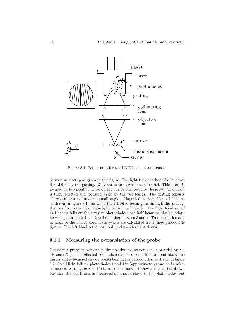
34 Chapter 3. Design of a 2D optical probing system
grating
laser
photodiodes
LDGU
1234
stylus
mirror
objectivelens
elastic suspensiony
z x
+ collimatinglens
+
Figure 3.1: Basic setup for the LDGU as distance sensor.
be used in a setup as given in this figure. The light from the laser diode leavesthe LDGU by the grating. Only the zeroth order beam is used. This beam isfocused by two positive lenses on the mirror connected to the probe. The beamis then reflected and focussed again by the two lenses. The grating consistsof two subgratings under a small angle. Magnified it looks like a fish boneas drawn in figure 3.1. So when the reflected beam goes through the grating,the two first order beams are split in two half beams. The right hand set ofhalf beams falls on the array of photodiodes: one half beam on the boundarybetween photodiode 1 and 2 and the other between 3 and 4. The translation androtation of the mirror around the y-axis are calculated from these photodiodesignals. The left hand set is not used, and therefore not drawn.
3.1.1 Measuring the z-translation of the probe
Consider a probe movement in the positive z-direction (i.e. upwards) over adistance Xtz . The reflected beam then seems to come from a point above themirror and is focussed on two points behind the photodiodes, as drawn in figure3.2. So all light falls on photodiodes 1 and 4 in (approximately) two half circles,as marked a in figure 3.3. If the mirror is moved downwards from the drawnposition, the half beams are focussed on a point closer to the photodiodes, but

3.1. The Laser Diode Grating Unit (LDGU) 35
z
ztX
x
y
Figure 3.2: Detection of vertical displacement Xtz of the probe.
still behind them (marked b, side view not shown). The half circle on photodiode1 and 4 will become smaller but still no light is falling on photodiode 2 and 3.Moving the mirror further downwards the light will be focussed on the boundarybetween the photodiodes which are now lighted equally (figure 3.3, c). Ideallythis is the rest position of the mirror. When the mirror is moved below thisposition the half beams are focussed in front of the photodiodes and they willflip to the other side of the separation line of the half beams (figure 3.3, d ande). So only photodiode 2 and 3 will be lighted. Due to this sharp transition, thedifference between photodiode 1 and 2 and between 4 and 3 is highly sensitiveto z-displacements of the mirror. A so called focal error signal (FES) can bedefined as [Bouwhuis 85]:
FES =I1 − I2 + I4 − I3I1 + I2 + I3 + I4
, (3.1)
where In is the photocurrent generated by photodiode n. The photocurrentis in good approximation proportional to the power of the light falling on thephotodiode. Because the FES is normalised by dividing by the sum of thephoto currents, the FES is in principle insensitive to variations in the laseroutput power. In practice there is some remaining sensitivity. According tothe theory described above, the dependence of FES on z-displacements wouldbe like shown in figure 3.3. When the mirror moves through the focal point of

36 Chapter 3. Design of a 2D optical probing system
1 22 1 21
a
a
e
side viewphotodiodes and
half beam
e
d
c
c
b
bottom viewphotodiodes 1 and 2
= FES(I1-I2)+(I4-I3)
I1+I2+I3+I4
a d ztXeb c
0
FES signal
Figure 3.3: The theoretical dependence of the FES on the probe displacementand the corresponding side and bottom views of photo diodes (one and twoonly) and one of the half beams.

3.1. The Laser Diode Grating Unit (LDGU) 37
the laser beam, the FES has a sharp transition from a maximum value to aminimum. During this transition a high sensitivity and hence a high resolutioncan be achieved.
The exact dependence of FES on the translation of the mirror depends on theexact position of the different elements. If, for example, the boundary betweenphotodiode 1 and 2 does not exactly coincide with the separation line of thehalf beam, the sensitivity for z-translation of the mirror decreases. Suppose theboundary is at the right side of the separation line. The flipping of the half beamoccurs when still falling completely on photodiode 1. When the size of the halfcircle increases it starts falling on photodiode 2. This makes it impossible topredict the relation between z-displacements and FES in advance. The relationshould be calibrated for each LDGU. Not withstanding this, it can be derivedthat the sensitivity of FES to z-translations of the mirror is proportional tothe focal distances of the lenses as:
dFES
dXtz
∼(
f1f2
)2, (3.2)
where f1 and f2 are the focal distance of the collimating and the objective lensrespectively. The proportionality only applies when the laser of the LDGU isin the focal point, a restriction which is usually met. Equation (3.2) is derivedin appendix B (equation (B.16)).
3.1.2 Measuring x-translation of the probe
The LDGU can also measure rotations around the y-axis. Suppose the probetip is moved in the positive x-direction (without considering vertical movementfor the moment). The mirror then rotates around the y-axis and the reflectedbeam in between the lenses shifts to the left, as can be seen in figure 3.4. Notethat the reflected beam is still focussed at the same point, apart from a cosineeffect due to the distance of the mirror plane to the axis of rotation (which liesin the plane of the slender rods). Because the diodes are in the focal plane ofthe first order half beams, the beams do not shift over the photodiodes. Thehorizontal displacement can be measured because the reflected beam is shiftedto the left at the position where it is split by the grating. So the left halfbeam has a greater portion of the total power than the right half beam. As thepower of the left half beam is measured by summing photocurrents 1 and 2,and the power of the right half beam by summing photocurrents 3 and 4, thedifference between these sums contains information on the angle of the mirror.The radial error signal (RES) is defined as this difference divided by the totaloptical power [Bouwhuis 85]:
RES ≡ I1 + I2 − (I4 + I3)
I1 + I2 + I3 + I4. (3.3)

38 Chapter 3. Design of a 2D optical probing system
X
xz
yR
L
+
+
tx
y
1234
Figure 3.4: Detection of a probe displacement in lateral direction.
In appendix B equation (B.30) the sensitivity of RES to a mirror rotation Ry
around the y-axis is calculated to be:
d(RES)
dRy
∼ f2f1
. (3.4)
Comparing this to equation (3.2), it is clear that the resolution in z-directionshould be weighted against the resolution in x-direction. Because the feasibilityof high accurate probing can be checked if at least one of the two directionshas a high resolution, it is decided not to sacrifice z-resolution for x-resolution.From an earlier research by Claesen it is known that a resolution of 1.5 nm canbe reached using focal lengths of f1 = 9 mm and f2 = 9 mm [Claesen 92]. TheRy-resolution is expected to be about 10 µrad (i.e. 40 nm for a 4 mm styluslength) for these focal lengths.
3.1.3 Cross talk between z- and x-measurement
Consider a simultaneous translation of the tip in both x- and z-direction. Dueto the rotation of the mirror, the power balance between the left wing (fallingon diodes 1 and 2) and the right wing (diodes 3 and 4) will be disturbed. Ifthe two wings have a different sensitivity to vertical mirror displacements, theFES will be disturbed by an x-translation of the tip. The sensitivity to vertical

3.2. Design of probe and suspension 39
mirror translations of the two wings can be different due to slight misalignmentsof the diodes, which makes the sensitivity unpredictable and probably differentfor each LDGU. Visscher measured this cross talk [Visscher 94]. He found thatthe difference in sensitivity is in the order of ten percent for a relatively largeangle of 100 mrad. Visscher used other lenses (f1 = 22.5 mm, f2 = 4.5 mm).Because the sensitivity for mirror rotation scales as f2/f1, see equation (3.4),his 100 mrad is to be compared to 20 mrad in our case, i.e. 80 µm probe tipdisplacement in x-direction. He also found that there is almost no sensitivity ofthe FES to probe displacements in y-direction.
The other way around, the RES is also sensitive for displacements of the mirrorin z-direction. From a plot in Visscher’s dissertation, it can be calculated thatthe sensitivity of the x-measurement to z-displacement is 0.12 for a 4 mm styluslength, i.e. a 100 nm z-displacement causes a FES reading of 12 nm. Softwareerror correction is probably needed for both cross talks.
3.2 Design of probe and suspension
The design of the probe, the intermediate body including the mirror, and thesuspension should be made together, because several of the parameters involvedare influenced by each other. Several requirements can be drawn up based onthe general requirements stated in chapter 1 and 2:
1. Good accessibility and visibility of the probe tip. Whether or not the probeis well accessible, highly depends on the workpieces to be measured. Forparts with typical dimensions of a few millimetre, a stylus length of 4 mmshould usually satisfy. Both the accessibility and the visibility of the probedegrade when the width of the suspension increases, as mentioned in theintroduction. A suspension which is not more than twice as wide as thelength of the stylus is taken as a reasonable limit. It should be possibleto use a small probe tip with a diameter of 0.3 mm in order to enable themeasurement of small holes.
2. High admissable probing speed. In chapter 2 it is explained that for areasonable probing speed of 1 mm s−1 and a probe tip diameter of 0.3 mm,the equivalent mass should be smaller than 20 mg and the stiffness shouldbe smaller than 200 N m−1. As lower values are preferred the stiffness inz-direction is set to 100 N m−1. It can be calculated by
cz = 3Eswst
3s
l3s, (3.5)
where Es is the Young’s modulus of the slender rod material, ls, ws, andts the length, width, and the thickness of the rods, as shown in figure 3.5.Equation (3.5) is deduced in appendix A, equation (A.13). The stylusand the intermediate body should be made as light as technically possible
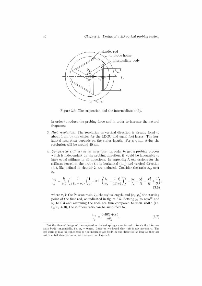
40 Chapter 3. Design of a 2D optical probing system
x
w
y
lxz
s
s
s
s
y
slender rodto probe house
intermediate body
Figure 3.5: The suspension and the intermediate body.
in order to reduce the probing force and in order to increase the naturalfrequency.
3. High resolution. The resolution in vertical direction is already fixed toabout 1 nm by the choice for the LDGU and equal foci lenses. The hor-izontal resolution depends on the stylus length. For a 4 mm stylus theresolution will be around 40 nm.
4. Comparable stiffness in all directions. In order to get a probing processwhich is independent on the probing direction, it would be favourable tohave equal stiffness in all directions. In appendix A expressions for thestiffness sensed at the probe tip in horizontal (cxy) and vertical direction(cz), like defined in chapter 2, are deduced. Consider the ratio cxy overcz.
cxycz
=l2s
2l2st
(1
2 (1 + νs)
(1
3− 0.21
(tsws− 1
12
t5sw5s
))− ys
ls+
y2sl2s
+x2sl2s
+1
3
),
(3.6)
where νs is the Poisson ratio, lst the stylus length, and (xs, ys) the startingpoint of the first rod, as indicated in figure 3.5. Setting ys to zero10 andνs to 0.3 and assuming the rods are thin compared to their width (i.e.ts/ws ≈ 0), the stiffness ratio can be simplified to:
cxycz
=0.46l2s + x2s
2l2st. (3.7)
10At the time of design of the suspension the leaf springs were forced to touch the interme-diate body tangentially, i.e. ys = 0 mm. Later on we found that this is not necessary. Theleaf springs may be connected to the intermediate body in any direction as long as they arenot oriented close to radial, as discussed in chapter 2.

3.2. Design of probe and suspension 41
Equal stiffness in every direction would require 0.46l2s + x2s = 2l2st, whichwould violate requirement 1 because the suspension would become at least2√
2 times as wide as the stylus length. Therefore non equal stiffness mustbe accepted. However, cxy and cz should not differ more than a factorof ten, because otherwise the difference between probing directions wouldbecome too large.
5. High admissable overtravel. The admissable overtravel, the smallest dis-placement of the tip before one of the slender rods plastically deforms orbreaks, is calculated in appendix A, equation (A.26). Neglecting shearstresses and setting ys to zero, the admissable overtravel Xovt can bewritten as:
Xovt = σYl2s lstEsts
√1
9x2s + 4l2s + 9l2st, (3.8)
where σY is the yield strength of the rod.
6. High natural frequency. The natural frequency should be maximised inorder to attenuate free oscillations of the probe which might cause falsetriggers. Besides, the bouncing of the probe after the first contact withthe workpiece will extinct faster if the natural frequencies are high. Thenatural frequencies can be calculated by
fn =1
2π
√ctm∗
(3.9)
where ct is the stiffness of the suspension in a certain direction and m∗ isthe equivalent mass in that direction as defined in the second chapter11 .Natural frequencies above a few hundred Hertz are preferred.
To achieve stiffnesses as close together as possible, it is decided to use all thespace allowed by requirement 1 for the suspension. Reserving about 1 mm toglue the slender rods to the probe house, this means that the suspension shouldnot be wider than 6 mm, i.e.
√l2s + x2s ≈ 3 mm. The admissable overtravel
can be maximised by choosing long and thin rods, made from a high yieldstrength material. The stiffness in z-direction can then be set by choosing thewidth. However, there are limits on this procedure. The space for long rodsis limited, the width should be at least an order smaller than the length toprevent overdetermination of the suspension, and sheet material is available ina limited number of thicknesses only. A spring steel with an yield strength ofabout 1500 N mm−2 has been chosen as suspension material. ls has been set
11Although it is more common to express the natural frequency for a rotational motion interms of angular moments and rotation, equation (3.9) is preferred because it is more generalsince it is also valid for pure translation and combinations of translations and rotations. It canbe easily seen that (3.9) is correct. Since m∗ is defined as the sensed mass when acceleratingin a certain direction, Newton’s law can be applied: m∗Xt + ctXt = 0. Inserting a trialsolution Xt = sin 2πfn and solving for fn proves equation (3.9).

42 Chapter 3. Design of a 2D optical probing system
parameters characteristicsrt = 0.015 mm
lst = 4 mmxs = 2 mmys = 0 mmls = 2 mmts = 20 µm
ws = 0.17 mmσY = 1500 N mm−2
cz = 100 N m−1
cxy = 18 N m−1
Xovt = 0.44 mmmeqz = 4.3 mg
meqxy = 0.69 mgfnz = 770 Hzfnxy = 810 Hz
Table 3.1: Parameters and characteristics of the probe and the suspension
to 2 mm because a larger ls will leave too few space for xs which would limitthe overtravel. An available thickness of 20 µm has been chosen. Adaptingthe width to get cz = 100 N m−1 it becomes 0.17 mm. About 2 mm is leftfor xs. A light weight aluminum intermediate body has been designed. Theupper surface has been diamond turned to get the requested mirror. A 0.2 mmdiameter tube, made from a hardened steel, has been used as stylus. The massof the intermediate body together with the probe is 4.3 mg. Their moment ofinertia around the x-axis can be calculated to be:
Ix =
∫(y2 + z2)ρ(x, y, z)dV = 1.1 · 10−11 kg m2 (3.10)
Due to symmetry, the moment of inertia around the x-axis is equal to themoment of inertia around any other axis in the xy-plane. The equivalent massfor the z-direction equals the above mentioned mass. The equivalent mass inx- and y-directions can be calculated by dividing the moment of inertia by thesquared stylus length:
m∗
xy =Ixl2st
= 0.69 mg. (3.11)
The natural frequencies can be calculated using (3.9):
fnxy =1
2π
√cxym∗xy
= 810 Hz (3.12)
fnz =1
2π
√czm∗z
= 770 Hz (3.13)
To conclude this section, the parameters of the probe and the suspension arecollected in table 3.1 together with the resulting characteristics.
3.3 Electronics
The photodiodes in the LDGU output a photo current proportional to thelight intensity falling on their surface. The maximum of this current is a few
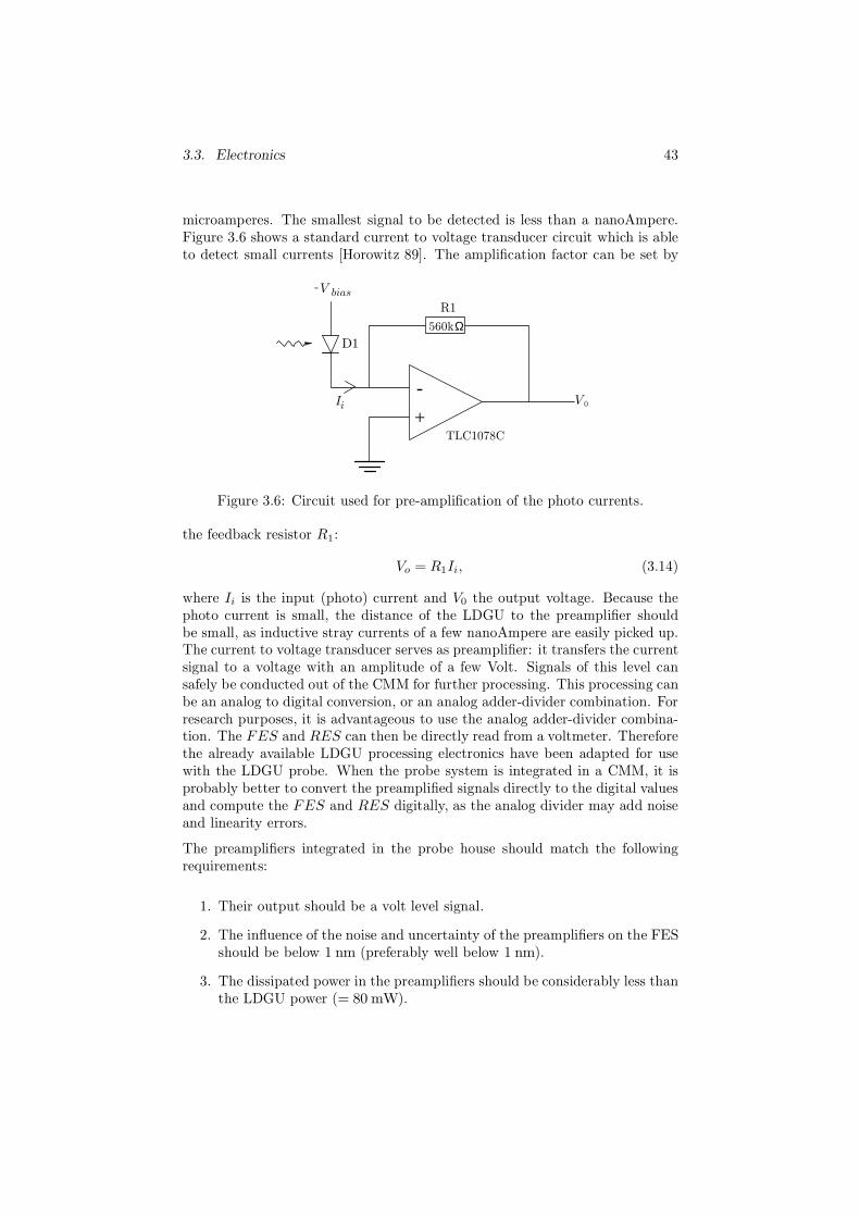
3.3. Electronics 43
microamperes. The smallest signal to be detected is less than a nanoAmpere.Figure 3.6 shows a standard current to voltage transducer circuit which is ableto detect small currents [Horowitz 89]. The amplification factor can be set by
V
I V
R1
bias
i 0
+-
TLC1078C
560kΩD1
-
Figure 3.6: Circuit used for pre-amplification of the photo currents.
the feedback resistor R1:
Vo = R1Ii, (3.14)
where Ii is the input (photo) current and V0 the output voltage. Because thephoto current is small, the distance of the LDGU to the preamplifier shouldbe small, as inductive stray currents of a few nanoAmpere are easily picked up.The current to voltage transducer serves as preamplifier: it transfers the currentsignal to a voltage with an amplitude of a few Volt. Signals of this level cansafely be conducted out of the CMM for further processing. This processing canbe an analog to digital conversion, or an analog adder-divider combination. Forresearch purposes, it is advantageous to use the analog adder-divider combina-tion. The FES and RES can then be directly read from a voltmeter. Thereforethe already available LDGU processing electronics have been adapted for usewith the LDGU probe. When the probe system is integrated in a CMM, it isprobably better to convert the preamplified signals directly to the digital valuesand compute the FES and RES digitally, as the analog divider may add noiseand linearity errors.
The preamplifiers integrated in the probe house should match the followingrequirements:
1. Their output should be a volt level signal.
2. The influence of the noise and uncertainty of the preamplifiers on the FESshould be below 1 nm (preferably well below 1 nm).
3. The dissipated power in the preamplifiers should be considerably less thanthe LDGU power (= 80 mW).

44 Chapter 3. Design of a 2D optical probing system
Due to the last requirement so called micro power operational amplifiers(opamps) are to be used. They are intended for use in battery powered ap-plications and need a supply current of ten to a few hundred µA. One of thelowest current opamps is the TLC1078C from Texas Instruments, consuminga supply current of 15 µA only. Besides this, it was selected because of its lowoffset current drift and noise, which are the most crucial noise and uncertaintydetermining parameters. A 560 kΩ feedback resistor is applied to reach a voltlevel output. A precision resistor is chosen because of its low temperature co-efficient (25 · 10−6 K−1), which is four times better than a standard metal filmresistor. Where possible, Surface Mounted Devices (SMD’s) are used to min-imize the dimensions of the printed circuit board. An error analysis for theFES, and the RES, including the electronics, is performed in appendix C.
3.4 Mechanical design and realisation
The main task of the probe house is the connection of the LDGU, the lenses,the suspension and the electronics to the CMM. Besides this it should shieldthe electronics for ElectroMagnetic Compatibility (EMC) and the LDGU andthe other optics for stray light. The positioning of the LDGU, the lenses andthe suspension to each other and to the CMM should be sufficiently accuratein order to reach the overall uncertainty of 20 nm. The effect of mispositioningof those elements do not have a one to one relationship to the measured value.How these uncertainties affect the FES and the RES is calculated in appendixC. In order to make an accurate FES measurement, it is important to positionthe LDGU and the two lenses accurately (positioning of the probe suspensionis less important). A design has been made which gives optimal positioning forLDGU and lenses. A cross section of the probe system is shown in figure 3.7
As the LDGU dissipated 80 mW, a temperature raise is to be expected. Mea-surements at other LDGU sensors with comparable dimensions show tempera-ture increases of about 2 K. As the natural convection caused by this tempera-ture difference is small, sensitivity to movement through the air can be expected.This means that the temperature of the probe house would vary depending onhow often and with what speed the CMM moves. This is unacceptable. There-fore a drain for the heat produced by the LDGU has been provided. The drainconsists of the LDGU mount and the heat sink mount (only partly shown infigure 3.7, the outside part of it can be seen on the photograph in figure 3.8).Both parts are made from aluminum because of its high thermal conductivity.The LDGU and its heat drain are isolated from the probe house by plastic,o-rings, or air. To limit the effect of residual temperature changes the probehouse and other position determining parts were made from invar. The plas-tic isolating parts and the aluminum thermal drain do not contribute to thethermal length. The steady state temperature raise of the housing is limited toabout 1 K, an improvement of a factor two compared to the conventional design.The steady state temperature raise of the drain is about 1.5 K. By adding a
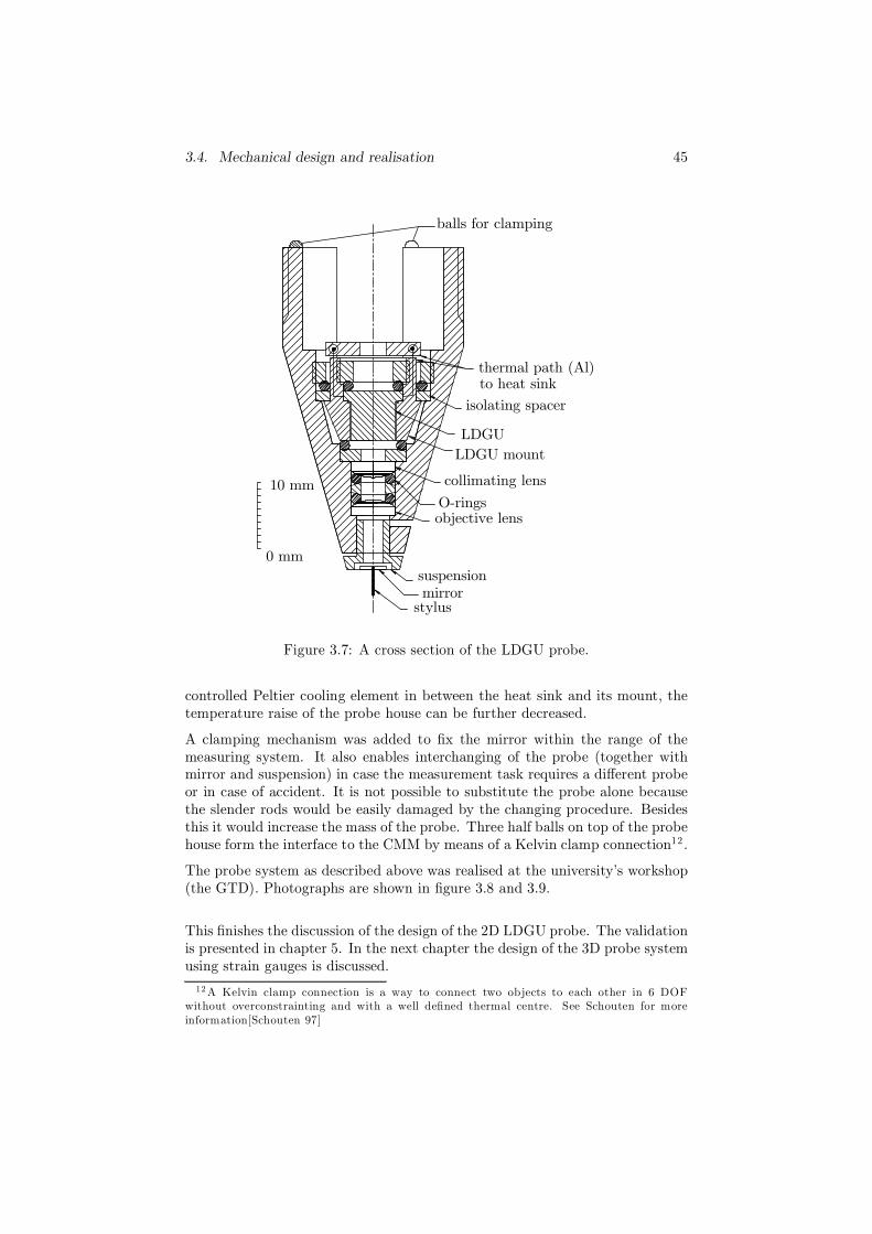
3.4. Mechanical design and realisation 45
thermal path (Al)
LDGU
collimating lens
objective lens
suspensionmirror
O-rings
stylus
0 mm
10 mm
balls for clamping
to heat sink
LDGU mount
isolating spacer
Figure 3.7: A cross section of the LDGU probe.
controlled Peltier cooling element in between the heat sink and its mount, thetemperature raise of the probe house can be further decreased.
A clamping mechanism was added to fix the mirror within the range of themeasuring system. It also enables interchanging of the probe (together withmirror and suspension) in case the measurement task requires a different probeor in case of accident. It is not possible to substitute the probe alone becausethe slender rods would be easily damaged by the changing procedure. Besidesthis it would increase the mass of the probe. Three half balls on top of the probehouse form the interface to the CMM by means of a Kelvin clamp connection12 .
The probe system as described above was realised at the university’s workshop(the GTD). Photographs are shown in figure 3.8 and 3.9.
This finishes the discussion of the design of the 2D LDGU probe. The validationis presented in chapter 5. In the next chapter the design of the 3D probe systemusing strain gauges is discussed.
12A Kelvin clamp connection is a way to connect two objects to each other in 6 DOFwithout overconstrainting and with a well defined thermal centre. See Schouten for moreinformation[Schouten 97]

46 Chapter 3. Design of a 2D optical probing system
probe unit
heat sink
thermal path
Figure 3.8: Picture of the 2D optical probe system
tip
stylus
slender rod
intermediatebody
Figure 3.9: Detail of the 2D probe system showing the probe and the suspension.

Chapter 4
Development of a 3D probe
system using strain gauges
In this chapter the development of a 3D measuring probe system based on piezo-resistive strain gauges is described. The strain gauges need to be placed on theslender rods. They cannot be glued on the rods for a number of reasons. First,the glueing is difficult due to the small dimensions of the rods (their widthis typically a few tenth of a millimetre). Second, the relation between strainson the surface of the rods and strain in the strain gauges would suffer fromhysteresis due to the glue which connects them. Finally, the electrical connectionwires would disturb the stiffness of the suspension in an unpredictable way.Using micromachining the strain gauges can be manufactured together with theslender rods and the electrical connections. An introduction to micromachiningis given in the first section of this chapter. In the next section the choice for thevalue of important parameters of the probe system is explained. An optimisationalgorithm is introduced that facilitates the optimisation. It makes use of thetheory described in appendix A. In the third section the design of the electronicsis described. Finally the probe house, the realisation of the suspension, and theassembling of the individual parts to a complete probe system is discussed.
4.1 Introduction to micromachining
Micromachining is the technology by which so called Micro Electro MechanicalSystems (MEMS’s) are made. By a series of deposition, lithography, and etch-ing steps complete systems including actuators, sensors and electronics can bemanufactured. Micromachining is derived from integrated circuit technology,from which it inherits properties like batch processability and consequent lowproduction cost for large series. Micromachining is nowadays employed mainlyfor pressure sensors, inkjet printing heads, and accelerometers (used e.g. in
47
48 Chapter 4. Development of a 3D probe system using strain gauges
airbags). Future applications are micropumps for dosing in medicine, adaptiveoptics, and flow sensors. The basic material for these devices is mostly sili-con, as is the case for IC technology. The finest details are limited to about amicrometre. The maximal dimensions are in theory limited by the dimensionsof the silicon wafer used; in practice, most MEMS’s have outer dimensions ofa few millimetre or less. In principle only two dimensional structures can bemade, however, certain three dimensional structures are possible too (sometimescalled 2.5 D). For more information, the reader is deferred to Sensors editedby Middelhoek [Middelhoek 89], the Handbook of Microlithography, Microma-chining and Microfabrication edited by Ray-Choudhury [Ray-Choudhury 97],or lecture notes used at the Twente MESA institute [Elwenspoek 96].
Three different basic micromachining techniques for making MEMS can be dis-tinguished, which are discussed below:
4.1.1 Bulk micromachining
The basic concept of bulk micromachining is to create mechanical features byremoving material from the wafer. Typically this is done by an sequence oflithography steps followed by a anisotrope wet etching which is explained insection 4.4.2. The wet etching removes the unwanted silicon and the desiredstructure is left behind. Most pressure sensors and accelerometers are manufac-tured using this technique, as is the 3D probing system being described in thischapter.
4.1.2 Surface micromachining
By surface micromachining mechanical features are formed on top of the siliconwafer. With this technique it is possible to make complex structures such asmotors and other actuators, micropumps and a number of physical and chemicalsensors. Mechanical features are formed by subsequent deposition, lithography,and etching of thin layers. Two different films are used: structural films andsacrificial films. The structural films form the later mechanical parts, while thesacrificial films are etched away in the final step to provide the needed spacebetween the parts. Typically polysilicon is used as a structural material, whilesilicon dioxide is used as a sacrificial material. At the end of the process, wafersare immersed in hydrofluoric acid, which quickly removes the silicon dioxidelayers, leaving the structural polysilicon layers untouched.
4.1.3 Mould micromachining
A third fabrication technology for creation of MEMS is mould micromachining.In this technology, mechanical features are created by first creating a mould.

4.2. Design of the probe and the suspension 49
The mould is then filled with a structural material to create the desired me-chanical devices. The mould can be etched away, or the mechanical devicecan be removed from the mould. The most famous mold micromachining tech-nology is LIGA, an German acronym for LIthographie, Galvanoformung undAbformung, i.e. lithography, electroplating and moulding. LIGA creates small,precise mechanical structures in the following way. A masks is created contain-ing the shape of the desired mechanical structures. Then, a cyclotron radiationsource is used to expose a thick resist layer. The irradiated area of the resistlayer is then dissolved using an appropriate developer, leaving a mould behind.Electroplating of copper, nickel or other metal into the mould then creates thedesired mechanical structure. Finally the remainder of the resist is dissolved.
4.2 Design of the probe and the suspension
The design of the probe, the intermediate body, the suspension, and the mea-surement system should be made at the same time, because several of the pa-rameters involved are influenced by each other. This is different from the LDGUprobe system where the design of the suspension and measurement system canbe split and optimised separately. The requirements are equal to the ones madeup in section 3.2. They are repeated here in short form in table 4.1 togetherwith the parameters that can be used for optimisation, as is explained later.
To meet the requirements, parameters describing critical parts of the probe sys-tem may be varied. These parameters are ls, ws, ts, xs, ys, and lst, which areall defined earlier in the text (e.g. in figure 3.5) as well as in the nomenclature.The requirements do not fully prescribe the value of the parameters. There isroom for further optimisation. The direction in which a characteristic shouldmove to reach a better probe system is given in the column ‘objective’ in table
Characteristic requirement objective determined byls ws ts xs ys lsl
cxy/cz > 0.1, < 10 close to 1 x (x) (x) x x xcz [ N m−1] < 200 N m−1 x x xlst [mm] > 4 mm large x
resolution [ nm] < 20 nm small x x x x x xovertravel [mm] large x x x x x x
D [mm] < 2lst small x (x) x xfn [ Hz] > 100 Hz high x x x x x x
Table 4.1: Overview of the characteristics, requirements, and objectives of theprobe system as wel as the parameters that determine the characteristics, in-dicated by an x in the appropriate column; (x) is used to indicate a weakcorrelation.
50 Chapter 4. Development of a 3D probe system using strain gauges
4.1. The number of crosses in the ‘determined by’ columns show that charac-teristics and parameters are linked in a complex way. The exact dependenceof most characteristics is given in appendix A: cxy in equation (A.12), cz in(A.13), the resolution in (2.17), where s3 is the smallest singular value of A ascalculated in (A.38), and the overtravel as calculated in (A.33). D is defined asthe diameter of the suspension. It is mainly determined by the starting point ofthe slender rod (xs, ys) and the length of the rod ls. To a lesser extend it alsodepends on the width of the rod bs. The natural frequency can be calculatedin the same way as it is done in chapter 3 equations (3.9) to (3.13). In practiceit appeared to be difficult to find the right change of parameters to change acertain characteristic at the expense of another. To overcome this difficulty,the optimisation is done using a numerical iterative procedure. The aim is notto let the computer decide which is the best compromise, but to give a goodpossibility. By shifting accents from the one to the other characteristic, this willeasily converge to what is believed to be the optimal probe system. This willbecome more clear by explanation of the optimisation mechanism.
Any optimisation algorithm requires an optimisation criterium, i.e. a numberwhich states the merit of a design relative to other designs. This criteriumcan be implemented by defining a cost function for each of the characteris-tics [Levoisier 97]. The criterium, or the total cost function, is defined as theweighted sum of the individual cost functions. Prior to defining cost functions,some simplifications can be made that work well in practice. The value ofcz is not really important as long as it is smaller than 200 N m−1, being therequirement. In practice, setting cz appears to have little effect on other char-acteristics. In order to be on the safe side, cz is set to 100 N m−1. For practicalprobe systems it appears that the natural frequency is always above 500 Hz.As this is high enough and yet higher values won’t bring much advantage, thenatural frequency characteristic is not taken into account in the optimisationroutine. There was an urge for higher stylus lengths. This implies either a lowstiffness ratio cxy/cz, or a large suspension outer size D. The latter is limited bypractice: it is undesirable to have one suspension filling a complete wafer. D istherefore set to 10 mm, so that six suspensions fit on a three inch wafer (beingthe wafer size used by the manufacturer). For the remaining characteristics,stiffness ratio, stylus length, overtravel, and resolution, cost functions should bedefined. The total cost function is defined as:
ftot = wsrfsr
(cxycz
)+ wlstflst (lst) + wovtfovt (xovt) + wresfres (xres) , (4.1)
where fsr, flst, fovt, and fres are the cost functions for the stiffness ratio cxy/cz,the stylus length lst, the maximal overtravel xovt, and the worst case resolutionxres respectively. wsr, wlst, wovt, and wres are the accompanying weight factors.As stated earlier, cxy, cz, xovt, and xres are calculated in appendix A. The costfunctions should reflect the relative size of the benefits, e.g. increasing the styluslength from 4 to 6 mm is a bigger improvement than increasing it from 10 to12 mm, so the stylus length cost function should be flatter near 10 mm than near4 mm. The exact formulation however is not really important, as will be shown.

4.2. Design of the probe and the suspension 51
For stability of the optimisation process, it is preferred to define nonlinear costfunctions. The cost functions used are plotted in figure 4.1.
0 5 10 150
0.5
1
cost function stylus length
l [mm]
cost
0 5 10 150
0.5
1
1.5cost function resolution
res [nm]
cost
0.2 0.4 0.6 0.8 10
0.5
1
1.5
2cost function overtravel
ovt [mm]
cost
0 0.2 0.4 0.6 0.8 10
0.2
0.4
0.6
0.8
1cost function stiffness ratio
c /c
cost
st
xy
Figure 4.1: Plots of the cost functions used to optimise certain parameters ofthe probe system. The functions give the relative penalty of the most importantprobe system characteristics. Low values correspond with preferred character-istics.
The weight functions take over the role of the probe system parameters as ‘ad-justment knobs’. For each set of weight functions the computer calculates andoutputs the optimised probe system parameters and the resulting characteris-tics. In an iterative process, the weight functions are adjusted based on theresults of the computer optimisation. This way the accents can be shifted tothe characteristics that are regarded as most important. An iteration could forexample look like the ‘trials’ given in table 4.2. The first attempt, trial one withall weight factors set to one, reaches a probe system with a very short styluslength. So the stylus length weight factor is increased to 5. The second attempthas a good stylus length at the expense of the resolution. The overtravel ishigher than needed so we can give away part of that. The third attempt istherefore done with an increased resolution weight factor and a decreased over-travel weight factor. The last step is fine tuning, no large changes are appliedrelative to the third one. If this approach is followed, the choice of the costfunctions is not really important. A suboptimal choice will cause a first trialthat is far off from the ideal probe system. By a few extra iterations, however,
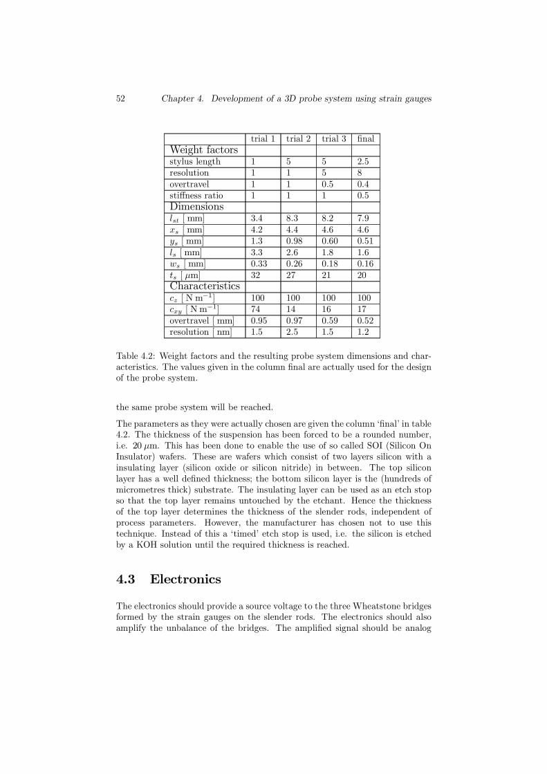
52 Chapter 4. Development of a 3D probe system using strain gauges
trial 1 trial 2 trial 3 finalWeight factorsstylus length 1 5 5 2.5resolution 1 1 5 8overtravel 1 1 0.5 0.4stiffness ratio 1 1 1 0.5Dimensionslst [mm] 3.4 8.3 8.2 7.9xs [mm] 4.2 4.4 4.6 4.6ys [mm] 1.3 0.98 0.60 0.51ls [mm] 3.3 2.6 1.8 1.6ws [mm] 0.33 0.26 0.18 0.16ts [ µm] 32 27 21 20Characteristicscz [ N m−1] 100 100 100 100cxy [ N m−1] 74 14 16 17overtravel [mm] 0.95 0.97 0.59 0.52resolution [ nm] 1.5 2.5 1.5 1.2
Table 4.2: Weight factors and the resulting probe system dimensions and char-acteristics. The values given in the column final are actually used for the designof the probe system.
the same probe system will be reached.
The parameters as they were actually chosen are given the column ‘final’ in table4.2. The thickness of the suspension has been forced to be a rounded number,i.e. 20 µm. This has been done to enable the use of so called SOI (Silicon OnInsulator) wafers. These are wafers which consist of two layers silicon with ainsulating layer (silicon oxide or silicon nitride) in between. The top siliconlayer has a well defined thickness; the bottom silicon layer is the (hundreds ofmicrometres thick) substrate. The insulating layer can be used as an etch stopso that the top layer remains untouched by the etchant. Hence the thicknessof the top layer determines the thickness of the slender rods, independent ofprocess parameters. However, the manufacturer has chosen not to use thistechnique. Instead of this a ‘timed’ etch stop is used, i.e. the silicon is etchedby a KOH solution until the required thickness is reached.
4.3 Electronics
The electronics should provide a source voltage to the three Wheatstone bridgesformed by the strain gauges on the slender rods. The electronics should alsoamplify the unbalance of the bridges. The amplified signal should be analog
4.3. Electronics 53
digital converted either by the electronics or by an Analog to Digital Converter(ADC) board in the computer. Two possibilities have been regarded:
1. Custom made electronics consisting of a preamplifier and an ADC with in-tegrated programmable gain amplifier, digital filter and 2.5 V DC voltagereference, among others used to supply the Wheatstone bridge.
2. Commercial electronics. In this case the bridge is supplied by an ACvoltage. An ADC board in the computer is used to convert the outputsignal to the digital domain.
The custom made electronics can be small volume and low power dissipating sothey can be integrated in the CMM. Therefore only digital signals run trough theCMM which are less sensitive to interference. The digital wiring can probablyleft unshielded and can therefore be more flexible and less disturbing to theCMM. As the Wheatstone bridge is supplied by a DC voltage, the capacitivecoupling in the MEMS and the connections cannot influent the measurement. Anegative consequence of this is that 1/f -noise13 of the electronics may contributesignificantly. Finally the electronics can be better adapted to the measurementproblem because they are custom made.
The commercial electronics use a AC voltage to supply the bridge. Thereforethe noise band is essentially shifted to around 5 kHz, being the frequency of thesupply voltage. 1/f -noise is therefore not expected to contribute significantly.On the other hand, capacitive coupling may influence the measurement. Smallvoltages must be transferred through the CMM. To prevent interference thewires should be well shielded which makes them stiffer. As it concerns ‘of theshelf’ electronics, time can be saved.
Both were tried with a dummy bridge consisting of four standard metal filmresistors and they both show a peak to peak noise band of around 1 µV V−1.Therefore, concerning noise there is no preference for the one or the other elec-tronics. The custom made electronics were chosen mainly because they can beintegrated with the probe. There is an extra argument for the custom madeelectronics which may, retrospectively, not be valid. The MEMS in combinationwith commercial electronics suffered from stability problems. This was causedby cross-talk between the different bridges due to too aggressive wire bonding.This caused leakage resistances to the substrate in the order of megaohms, whichwere, however, non constant, and showed hysteresis and voltage dependence. Itis likely that AC electronics are disturbed more than the DC electronics dueto the hysteresis of the leakage resistors. Newer probes are improved in thisrespect, although the problem may not have been completely solved. Due totime shortage, the newer probes have not been tried in combination with thecommercial AC electronics.
131/f noise is noise with a frequency spectrum proportional to 1/f . It is also called flickeror pink noise. More information can be found in Horowitz and Hill [Horowitz 89].

54 Chapter 4. Development of a 3D probe system using strain gauges
The custom electronics are built around the AD7710, an integrated circuit de-signed for conditioning and interfacing of a high accuracy Wheatstone Bridge.Main components are, among others, a voltage reference, a Programmable GainAmplifier (PGA), a Σ-∆ type 24 bit ADC with a serial output, and a dig-ital filter. A circuit showing the most important elements is given in figure4.2. The circuit is duplicated three times, one for each of the Wheatstone
2.5 V
Vref
INA118
C110 nF
R1 R2
R3 R4
R5
R6
R7
R8
AD7710
50k
27k
100k
50k
ADC
serialout24 bit
PGA
Ω
Ω
Ω
Ω
--
++
Figure 4.2: Circuit showing the most important elements of the custom madeelectronics built to interface each of the three Wheatstone bridges formed bythe strain gauges on the slender rods.
bridges. The 2.5 V voltage reference is used to supply the Wheatstone bridgeconsisting of R1 to R4. R5 limits the power dissipated in the bridge. ForR1 ≈ R2 ≈ R3 ≈ R4 ≈ 10 kΩ (one of the nominal values for the received sus-pensions), the power dissipated in each resistor is about 11 µW. The resistorsR6 to R8 are used to balance the bridge assuring that the input voltage of thepre-amplifier is close to zero. C1 is added to gently filter the bridge outputsignal with a frequency well above what could possibly be a real signal. The−3dB frequency of the filter depends on the nominal resistance of the straingauge resistors. For 10 kΩ resistors the frequency is 2.5 kHz, which can be veri-fied using the equivalent circuit given in figure E.4 in appendix E. Although theAD7710 has its own PGA on board, it has been decided to add a pre-amplifierwith improved noise characteristics. The input noise of the AD7710 is specifiedto be 0.25 to 1 µV RMS, depending on the PGA amplification and the digitalfilter settings. Since a relative resistor change of 10−6 should be measurable,the AD7710 is consuming almost all the error budget. It has therefore been de-cided to add a pre-amplifier (the INA118, an instrumentation amplifier), whichhas better noise performance: 0.28 µV top top in the range 0.1 to 10 Hz. Thisimplies a relative resistance change of 0.3 ·10−6 can be measured using a bridgesupply voltage of 1 V.

4.4. Realisation 55
4.4 Realisation
4.4.1 Probe house
The function of the probe house is the interfacing of the probe to the CMMand the shielding of the MEMS both mechanically as electromagnetically, as isthe case with the LDGU probe. In case of a MEMS the last function is calledpackaging. The probe house itself is kept as simple as possible (figure 4.3),consisting of a round 8 mm shaft providing the interface to the CMM and spacefor glueing the MEMS and a flexible print for the electrical connection.
stylus
flexible printstrain releaf
intermediate bodysilicon chip
glueing tool
probe house
bond pads
Figure 4.3: The assembled probe house
4.4.2 Photolithography and etching of the suspension,
strain gauges, and electrical connections
The individual steps in the fabrication of the suspension with the integratedstrain gauges and electrical connections is described rather comprehensive, toenable readers not familiar with lithography and etching techniques to followthe process. The process was developed by the manufacturer (Twente MicroProducts (TMP), taken over by Kymata Netherlands and Alcatel and latersplitted of as C2V). The starting point is a 3 inch 360 µm thick <100>14 wafer,polished on both sides. The more technical process flow for the micromachiningof the MEMS for the probe system is given in appendix D. First objective isto etch silicon from the bottom side of the wafer in order to get membranes
14Following common conventions, <100> is used to specify the (1,0,0) direction in a crystalas well as all equivalent directions due to the crystal symmetry, e.g. (-1,0,0), (0,1,0), etc[Ashcroft 76].

56 Chapter 4. Development of a 3D probe system using strain gauges
surrounded by edges of silicon of the original thickness. On this membrane, thestrain gauges and the electrical connections will be applied. Finally most of themembrane is etched away saving the slender rods and the outer structure of thesuspension only.
Etching of the membranes
The silicon etching until the requested membrane thickness is reached, is doneby a KOH solution. Places which should not be etched must be covered by aprotective layer, a mask, which is able to resist the etchant. This is done bycovering the whole wafer with silicon nitride, applied by a Chemical VapourDeposition (CVD) process. To pattern the mask, it is covered by a photoresist.The photoresist is exposed and developed. Then the parts not protected bythe developed photoresist are etched away by Reactive Ion Etching (RIE) byCHF3 and O2. The resist is removed by fumic HNO3. Finally the silicon isetched by KOH. A KOH etch is an example of a wet anisotrope etch, i.e. theetchant is a fluid and the etch rate depends on the crystal direction. KOH hasa deep minimum in the etch rate in <111> direction and a small one in <100>direction. This means that, provided the etch time is long enough, the etch pitis bounded by <111> and <100> planes. All other planes are readily attackedby the KOH and will disappear soon. In principle the <111> and <100> planesare perfectly flat. This gives the possibility of reducing the thickness of a <100>wafer. In practice it is not that ideal: the surface is roughened, probably due tothe forming of H2 bubbles which tend to stick to the surface, and hillocks arisedepending on the concentration of the KOH solution [Elwenspoek 96]. AlsoKOH appears to etch the middle of the membrane slower than at the edges. Toovercome the difference in etching speed, the KOH etch is done in two steps.First, only the centre part of the mask is removed and 30 µm silicon is etchedby KOH. Then the remainder of the mask is removed, except for those partsthat should remain thick, the stiff outer side of the suspension. Even withthis procedure, a 20 µm membrane thickness could not be reached. Minimalthickness appeared to be 40 µm. A bottom view and a cross-section of thewafer after the KOH etch are shown in figure 4.4 and 4.5.
Deposition of the strain gauges
First, a silicon nitride layer is deposed on the top side of the wafer to isolate thestrain gauges and the connections from the bulk silicon. Then a polycrystallinesilicon layer is deposed and doped with Boron. Resist is applied, exposed, anddeveloped. At the end of this step the polysilicon is covered by resist at theposition of the strain gauges only, i.e. two on each end of the future slenderrods. The polysilicon is removed, except for the strain gauges, by RIE with SF6and O2. A cross-section after this step is shown in figure 4.6.

4.4. Realisation 57
Figure 4.4: Rendered 3D bottom view of the membrane after a KOH etch.
silicon
silicon nitride
Figure 4.5: Cross-section of a part of the wafer showing the 40 µm thick mem-brane that will form the slender rods.
Deposition of the electrical connections
The bond pads and the electrical connections between the strain gauges and thebond pads are processed much like the strain gauges are formed. An aluminumlayer is deposed on top of the wafer and covered by resist. The resist is exposed,using an appropriate mask, and developed. The aluminum not covered by resistis etched away. Because the whole structure is going to be exposed to air, thetop side of the wafer is covered by protective silicon nitride coating. Figure 4.7shows the result after those steps.
Etching of the slender rods
Finally the slender rods and other geometric features are formed by etching thesuperfluous part of the membrane away. This requires the use of a chromiummask layer, just like the silicon nitride layer was used in the first series of stepsas a mask for the KOH etch. The chromium is covered by resist. The resist isexposed and developed. The partition of the wafer that should not be etched isnow covered by resist. After etching of the chromium, the unwanted silicon isremoved by RIE with SF6, CHF3, and O2. Finally the remaining chromium isetched away.

58 Chapter 4. Development of a 3D probe system using strain gauges
silicon
silicon nitride
polysilicon
Figure 4.6: Cross-section (not on scale) through one of the future leaf springsshowing the applied strain gauges.
siliconsilicon nitridepolysilicon
aluminum
Figure 4.7: Cross-section (not on scale) through one of the slender rods showingthe strain gauges (polysilicon), the electrical connections (aluminum), and thepassivation and insulation layers (silicon nitride).
4.4.3 Assembling
The individual parts, the tip, the stylus, the intermediate body, the suspension,the flex cable, and the probe house, are to be connected to each other. Theprocedure is set by the availability of tooling, and the fragility of the chip. Mostparts are glued together, because there is little other option. The end of the flexcable is electrically connected to the bond pads on the suspension by ultrasonicwire bonding.
The probe house including the glueing tool is manufactured at the TU/e work-shop. It is then send to TMP who made the chip. TMP glues the chip andthe flex cable to the probe house and electrically connects the flex cable withthe bond pads on the chip by wire bonding. At the TU/e there is no facilityto wire bond aluminum. In the mean time, the TU/e workshop assembles thetip, stylus and intermediate body. The probe house suspension subassembly issent back to the TU/e. Finally the intermediate body and probe subassemblyis glued to the suspension. This the most dangerous step. A glueing tool is pro-vided inside the probe house. The tool can be gently shifted upwards againstthe slender rods to support the suspension during the applying of the glue andintermediate body to the suspension. After the glue has hardened, the glueingtool is to be retracted. After this step the probe system is ready to be used.
Photographs of the realised probe system are shown in figures 4.8 to 4.10. Notethe match that is used for size reference. Although probe systems with straingauges have been made before, the system described here with this size andaccuracy can only be made using micromachining techniques. With this a con-siderable step in the direction of more accurate and smaller probe systems hasbeen made.

4.4. Realisation 59
Figure 4.8: Side view of the realised prototype. A match is shown as a sizereference.
Figure 4.9: Top view of the realised prototype

60 Chapter 4. Development of a 3D probe system using strain gauges
R1
R4 R2
R3
Figure 4.10: Detail of the prototype showing one of the slender rods. The piezoresistive strain gauges R1...R4 can be seen in this detail.

Chapter 5
Verification of both probe
systems
In this chapter the verification of the probe systems presented in chapter 3 and4 is described. For complete calibration, the following items should be checked.
1. The behaviour of the measurement signals as a function of probe motion ina certain direction. Sensitivity, hysteresis, non-linearity, and reproducibil-ity can be determined by this measurement. The influence of the probingdirection on the sensitivity can be determined by repetitive measurementsin different directions.
2. The stability of the measurement signals of the probe system. In this casethe probe system is fixed to a well defined surface. The thermal loop iskept as short as possible. Stability and repeatability can be determinedin this setup. The time for which stability is requested is one hour.
In principle, all measurements can be performed using a small volume CMM.The uncertainty of the CMM, however, should be substantially better thanthe expected uncertainty of the probe system under test, i.e. 20 nm. As suchCMM’s did not exist at the time the measurements were done, other solutionshad to be found.
A 1D calibration setup, called calibrator in the remainder of this thesis, canbe used if the probe system is positioned on the calibrator in several differentorientations. A 1D calibrator consists of a platform to which the probe systemto be calibrated has to be attached, and a moving surface actuating the probe,preferably in the centre of the platform. The displacement of the moving surfacerelative to the platform is determined by a measurement system, which shouldbe more accurate than the probe system under test.
61

62 Chapter 5. Verification of both probe systems
Such a calibrator was designed and manufactured and is described in the firstsections. The verification of the strain gauge and the LDGU probe system usingthis setup is discussed in the remaining sections.
5.1 Design of the calibrator
The specifications of a calibrator, as described shortly in the introduction ofthis chapter, should be better than the probe system itself. A calibrator withthe following specifications fulfils this need:
• uncertainty smaller than 10 nm when used in a environment with temper-ature changes of at most 100mK.
• resolution smaller than 1 nm
• range at least 30 µm.
A likewise specified calibrator will be more accurate than the probe system, willhave a resolution comparable to the expected resolution of the probe system,and will be able to cover the most interesting measurement range of the probesystem. Nevertheless, it is still possible to design the calibrator using of theshelf components like a laser interferometer and a piezo crystal actuator, as isshown in the remainder of this section.
The strain gauge probe system is calibrated in three dimensions by repetitive1D measurements with different orientations of the probe system with respectto the calibrator. This procedure is valid if two conditions are met:
1. The orientation of the probe system with respect to the moving axis ofthe calibrator should be known accurately enough.
2. The behaviour of the probe system does not depend on the orientation ofthe probe system, e.g. the turning of a vertically oriented probe systemto any horizontal position may not influence the functioning of the probesystem apart from a different rest position.
A deviation of the actual orientation of the probe system relative to the intendedorientation causes angle errors in the matrix A15 . This means that misposition-ing causes errors relative to the displacement of the probe. The orientation ofthe probe system should therefore be known better than the intended relativeerror of the probe system, i.e. for 4 µm moves and 1 nm uncertainty, the posi-tioning angle of the probe system relative to the axis of motion of the calibratorshould be known with an uncertainty of 1 · 10−9/4 · 10−6 = 0.25 mrad.
15A matrix like defined in (2.15) and (A.38), which transforms a displacement of the probetip to excitation voltages of the Wheatsone bridges.

5.1. Design of the calibrator 63
Gravity is the only effect that may disturb the behaviour of the probe system inother than vertical orientations. Due to the weight of the probe and the inter-mediate body the rest position of the tip will alter. However, there is no reasonfor the sensitivity to change. The rest position is unimportant because onlyrelative displacements (relative to a certain start position) are to be measured.For this reason the orientation of the probe system may be chosen as desired.
A cross-section of the basic setup of the calibrator is shown in figure 5.1. A mea-surement mirror (4) can be displaced relative to a ring shaped reference mirror(1) by a piezo actuator (3). This displacement is measured by a differentialflat mirror interferometer (19). The probe system to be calibrated (16) is me-chanically connected to the reference mirror via the platform of the calibratorand a separate bracket (14). The probe is positioned against the measurementmirror. To perform a coarse adjustment of the calibrator to the probe system,the reference mirror together with the measurement mirror and the piezo canbe displaced over about a millimetre. The laser interferometer setup and the
16 14
1
4
2
3
19
12
23
Figure 5.1: Configuration of the calibration setup. 1: reference mirror, 2: plat-form, 3: piezo actuator, 4: measuring mirror, 12: frame, 14: probe bracket, 16:probe system, 19: interferometer, 23: laser source and receiver. The numberscoincide with the numbers in figures 5.5 and 5.6. d is the distance between theincomming and the returning beam.

64 Chapter 5. Verification of both probe systems
mechanics of the calibrator will be discussed below. At the end of this sectionan error analysis is given.
5.1.1 The plane mirror differential laser interferometer
setup
The flat mirror differential laser interferometer setup shown in figure 5.2 can beused to measure the displacement of the one mirror relative to the other. Itsmerits are listed below:
• The two mirrors can be close to each other which decreases the thermalloop of the calibrator.
SSSS SSSSm m
SSSS ˜ ˜r
SSSSr
SSSSb1
SSSSb 2
SSSSi
SSSScc
xy
z
probe
from laser
to laser1
4
a
λ
d
Figure 5.2: Optics for the differential flat mirror interferometer. The mirrorsare labeled: Si: interferometer (a polarising beam splitter), Scc: corner cube(retro reflector), Sb1: first bending mirror, Sb2: second bending mirror, Sm:measurement plane mirror, Sr: reference plane mirror. The second reflectionof the measurement and reference mirror is indicated by a tilde (Sm and Srrespectively). The quarter wavelength plates are indicated by a dashed boldline. The measurement and the reference beams are indicated by a continuousand a dashed line respectively. The x-axis is aligned along the outgoing beamsof the laserhead, the z-axis is aligned along the measurement axis, and theorigin is placed in the middle of the laser opening and the receiver. The a-axisis defined as an axis in (-1,0,1)-direction.

5.1. Design of the calibrator 65
• The reference and measurement mirror can be positioned symmetricallyaround the measurement axis which preserves the cylindrical symmetryof the calibrator.
• The mass of the measurement mirror can be small, improving the dynam-ical properties of the calibrator.
• Both beams reflect two times at the reference or measurement mirrorcausing a double pass and hence double sensitivity compared to an inter-ferometer setup with two corner cubes.
• Both beams travel equal distances through the concerning media (air andglass), provided that the flat mirrors lie in the same plane. A changein refractive index, e.g. due to a homogeneous temperature or pressurevariation, will effect both beams equally and will therefore not disturb themeasurement.
The setup has one major drawback: Both parallelism of the returning beams asthe accuracy of the measurement depend on alignment and quality of the usedmirrors. Elements requiring special precautions are the first bending mirror,that should be parallel to the interferometer mirror, and the reference, mea-surement, and second bending mirror, that have tough flatness specifications.These requirements are explained and quantified in the next section.
Matrix description of the optical system
A matrix model of the interferometric setup is made and described in thissection. Using this model, the sensitivity of the system to displacements orrotations of any of the mirrors can be quantified. First the definition of amirror matrix used in the remainder of this section is given.
Rays passing through an optical system consisting of plane mirrors only undergoa linear transformation [Brouwer 64]. Like any plane, a plane mirror can be de-scribed in any Carthesian coordinate frame by a normal vector n = (nx, ny, nz)
(with |n| = 1 by definition) and a point P = (px, py, pz) on the mirror. Suppose
a certain point A is mirrored to A′. For the transformation of a point A to A′
homogeneous coordinates are used: A = (ax, ay, az, 1), A′ =(a′x, a
′
y, a′
z,1). The
matrix describing this transformation is [Brouwer 64]:
S(n, P
)=
1− 2n2x −2nxny −2nxnz 2nx (nxPx + nyPy + nzPz)−2nxny 1− 2n2y −2nynz 2ny (nxPx + nyPy + nzPz)−2nxnz −2nynz 1− 2n2z 2nz (nxPx + nyPy + nzPz)
0 0 0 1
.
(5.1)
Also the change of the beam direction through the optical system can be de-scribed by S: The transformation of a beam with direction r = (rx, ry, rz) to

66 Chapter 5. Verification of both probe systems
r′ =(r′x, r
′
y, r′
z
), with |r| = |r′| = 1, can be described by a matrix formed
by the first three rows and columns of S [Brouwer 64]. Equivalently the com-plete matrix S can be used provided that r is expanded with an extra zero:r = (rx, ry, rz ,0). This prevents the defining of new 3 × 3 matrices and istherefore preferred. If the system consists of more than one mirror, the result-ing mirror matrix Sres can be calculated by multiplication of the individualmatrices in proper order:
Sres = SnSn−1...S1, (5.2)
where S1 describes the first mirror in the beam path and Sn the last.
To describe the transformation of the measurement and reference beam, mirrormatrices are introduced in table 5.1. The nominal positions and orientationsin this table can be determined from figure 5.2. Also the coordinate frame isgiven in this figure. ∆P adds a small variance to each of the nominal positionsin an arbitrary direction. ∆n is the variance in the normal direction of eachmirror due to a small rotation around two axes in the plane of the mirror, i.e.rotation around the x- or y-axis for the reference and the measurement mirror(Rrx, Rry, Rmx, and Rmy), and rotation around the a-axis (an axis in (−1, 0, 1)direction) and the y-axis for the bending mirrors and the interferometer (Ria,Riy, Rb1a, Rb1y, Rb2a, and Rb2y). Any of the mirror matrices Sx is calculatedusing equation (5.1) and the sum of the variances and the nominal positionsand orientations from table 5.1:
Sx ≡ S(nx + ∆nx, Px + ∆Px
), (5.3)
where x = i, b1, b2, r, or m. For the reference and the measurement mirroralternative matrices have been introduced marked by a tilde. These alternativesare used to study the effect of unflatness of these mirrors: The first time a beamis reflected by the measurement or reference mirror, the normal mirror matrixSm, or Sr is used; the second time the alternative matrix with the tilde isused. Also for other mirrors alternative matrices for each reflection of eitherinterferometer beam could have been defined. This has been done, but is notworked here, because the procedure is comparable to measurement and referencemirror. The results are given later. The mirror matrix of the corner cube Scccan be calculated by multiplying three mutually orthogonal mirror matriceswith a common point at Pcc:
Scc =
−1 0 0 2 (Pccx + ∆Pccx)0 −1 0 2 (Pccy + ∆Pccy)0 0 −1 2 (Pccz + ∆Pccz)0 0 0 1
(5.4)
The matrix Sp describing the transformation of the measurement beam can becalculated by the multiplication:
Sp = SiSb1Sb2SmSb2Sb1SccSiSb2SmSb2, (5.5)

5.1. Design of the calibrator 67
Mirror matrices with name, nominal orientations and positions,and variationsSi interferometer
ni =(12
√2, 0, 12
√2)
∆ni =(12
√2Riy,Ria,− 1
2
√2Riy
)Pi = (pix,0, 0) ∆Pi = (∆pix,∆piy, ∆piz)
Sb1first bending mirror
nb1 =(12
√2,0, 12
√2)
∆nb1 =(12
√2Rb1y,Rb1a,− 1
2
√2Rb1y
)Pb1 = (pb1x,0, pb1z) ∆Pb1 = (∆pb1x,∆pb1y,∆pb1z)
Sb2 second bending mirror
nb2 =(12
√2,0, 12
√2)
∆nb2 =(12
√2Rb2y,Rb2a,− 1
2
√2Rb2y
)Pb2 =
(pb2x,0,
12pb1z
)∆Pb2 = (∆pb2x,∆pb2y,∆pb2z)
Sr reference mirrornr = (0,0, 1) ∆nr = (Rry,−Rrx,0)Pr =
(pb2x − 1
2dr, 0, prz
)∆Pr = (∆prx,∆pry, ∆prz)
Sm measurement mirrornm = (0, 0, 1) ∆nm = (Rmy,−Rmx, 0)Pm =
(pb2x + 1
2dm, 0, prz)
∆Pm = (∆pmx, ∆pmy,∆pmz)
Sr reference mirror
nr = (0,0, 1) ∆nr =(Rry,−Rrx, 0
)Pr =
(pb2x + 1
2dr, 0, prz
)∆ Pr = (∆prx,∆pry, ∆prz)
Sm measurement mirror
nm = (0, 0, 1) ∆nm =(Rmy,−Rmx,0
)Pm =
(pb2x − 1
2dm, 0, prz)
∆ Pm = (∆pmx, ∆pmy,∆pmz)Scc cube corner
Pcc = (pix,0, pccz) ∆Pcc = (∆pccx,∆pccy, ∆pccz)
Table 5.1: Mirror matrices definitions used to analyse the differential planemirror interferometer. A tilde implies a second reflection of this mirror. Thevariables are introduced in the text.
Which can be checked by tracking the measurement beam in figure 5.2. Like-wise the matrix Ss describing the transformation of the reference beam can becalculated as:
Ss = Sb2SrSb2SiSccSb1Sb2SrSb2Sb1Si (5.6)
The equations (5.5) and (5.6) can be used to calculate the direction of thereturning beams and the imaged position of the laser source.

68 Chapter 5. Verification of both probe systems
Direction of the returning beams
When both beams finally arrive at the receiver, the wave fronts of the mea-surement beam and the reference beam must be parallel to each other. If not,the beams will cause a line interference pattern over the surface of the photodiode which is supposed to detect the phase difference between both beams.In that case, displacement of the measurement or reference flat mirror causesa moving interference pattern over the surface, instead of an alternating lightdark sequence. The photo diode cannot detect the movement of the interferencepattern and will integrate the pattern to a constant value independent on thedisplacement of the flat mirrors. The laser interferometer setup can not func-tion this way, which is indicated by a close to zero signal strength. In order toprevent the line interference pattern on the photo diode, the angle between thewave fronts of the beams should be less than half a wavelength over the width ofthe beams, i.e. 316 nm over 6 mm or 50 µrad16 . As the wave fronts are alwaysperpendicular to the propagation direction of the beam, this requirement canbe equally well stated as: the angle between the direction of the reference andmeasurement beam should be less than 50 µrad.
The influence of orientation errors of all mirrors used on the direction of thelaser beams can be calculated using the mirror matrices (5.5) and (5.6) derivedpreviously:
−→rm = Sp−→r0 (5.7)
−→rr = Ss−→r0 , (5.8)
where −→rm and −→rr are the direction of the measurement and reference beam re-spectively when arriving at the receiver. −→r0 is the direction of both beams whenleaving the laser head and is by definition equal to (−1, 0, 0, 0)
T. Equations (5.7)
and (5.8) can be expanded using (5.5) and (5.6) and the parameters mentionedin table 5.1. When neglecting second and higher order variance terms, the resultis:
−→rm =
1
2√
2(Ria −Rb1a) + 2(Rmx −Rmx
)4 (Rb1y −Riy) + 2
(Rmy −Rmy
)0
(5.9)
−→rr =
1
2√
2(Rb1a − Ria) + 2(Rrx − Rrx
)4 (Riy − Rb1y) + 2
(Rry −Rry
)0
(5.10)
16The tolerance on the angle between the measurement and reference beam is not specifiedby the manufacturer (Agilent) directly. However, for plane mirror interferometry Agilentrequires a flatness of the mirrors of λ/4, which corresponds to the above calculated 50 µradspecification.

5.1. Design of the calibrator 69
From this result it can be seen that the angle between the beam directionsis eight times the rotation of the bending mirror around the y-axis and 4
√2
times the rotation around the a-axis. These results correspond to a numericalanalysis by Cuijpers [Cuijpers 95] for an equivalent interferometer setup. Nextto this, the result also shows that unflatness of the measurement or referencemirror influences the direction of the returning beams. The angle between thebeams should be smaller than 50 µrad, as discussed before. Therefore, the nextinequality should hold:
|−→rm −−→rr | =
∣∣∣∣∣∣∣∣∣∣
0
4√
2 (Ria −Rb1a) + 2(Rmx − Rmx
)− 2
(Rrx −Rrx
)8(Rb1y − Riy) + 2
(Rmy −Rmy
)− 2
(Rry − Rry
)0
∣∣∣∣∣∣∣∣∣∣
< 50 · 10−6 (5.11)
Effects of unflatness of the polarising beam splitter and the two bending mirrorscan be calculated in exactly the same way. This calculation, which is not workedout here, proofs that: (1) unflatness of the second bending mirror is up totwice as harmful as unflatness of the reference or measurement mirror, and (2)unflatness of the polarising beam splitter and the first bending mirror causesno pointing difference between the two returning beams.
The parallelism of the first bending mirror relative to the interferometer andthe unflatness of the reference, and measurement, and second bending mirrorshould be budgeted in order to satisfy (5.11). Based on estimated manufacturingpossibilities the individual specifications are set to:
• The first bending mirror must be parallel to the interferometer within4 µrad.
• Unflatness of the reference, measurement, and second bending mirrorcauses the local mirror normals of those mirrors to vary over the dif-ferent reflections on those mirrors. This angle variation must be smallerthan ±5 µrad. This is equivalent to an unflatness of λ/20 over a 6 mmdistance.
Manufacturing optics that meet these requirements is possible with reasonableeffort.
Translation of the image point by mirror translations and rotations
Translation of the image point due to translations or rotations of the mirrorsaffects the Optical Path Length (OPL) of the measurement and the reference
70 Chapter 5. Verification of both probe systems
beam. The location of the image points of the reference beam (Pr) and the
measurement beam (Pm) can be calculated using the above derived matrixes:
−→Pm = Sp
−→P0 (5.12)
−→Pr = Ss
−→P0,
where−→P0 is the output position of the laser source which is by definition equal
to(0, 0, 12d,1
)T, with d the distance between the incoming and outgoing beam
(see figure 5.2). As the nominal beam direction of the returning beams is thepositive x direction, the OPL difference (OPD) between the measurement andthe reference beam is determined by the difference in the x-coordinates of bothimage points. Using equation (5.12) this difference can be evaluated to:
OPD ≡ −→Pm
∣∣∣x− −→Pr
∣∣∣x
= 2(∆pmz + ∆pmz)− 2 (∆prz + ∆prz) + 4d (Rb1y −Riy) .
(5.13)
As expected, OPD depends on the distance between the reference and the mea-surement mirror. Next to this it is also sensitive to rotations of the first bendingmirror around the y-axis with respect to the orientation of the interferometer.This means that, for a measurement instability of 10 nm and a beam offset d= 12 mm, the angle around the y-axis between the first bending mirror and theinterferometer should be stable within 0.8 µrad. Rotation of the first bendingmirror or the interferometer around the a-axis has no first order effect on themeasured distance.
The same result can be obtained in a more intuitive way using figure 5.3. Thisfigure is used to show that parts of the OPL exist, which depend on mirrortilt differently for the measurement as for the reference beam. In principlethe direction of the reflected beam depends on the mirror tilt. However, themirror tilt dependence on the direction of the reflected beams has not beentaken into account because it only causes a second order effect in the OPLand a beam walk-off. Because mirror tilts under consideration are smaller thanone microradian, second order effects can safely be neglected. Beam walk-offis defined as a lateral displacement of the measurement beam in respect to thereference beam at the position of the detector. Beam walk-off does not causemeasurement errors, only a degradation of the signal strength if it has the sameorder of magnitude as the beam diameter.
First consider a tilt of the first bending mirror. This tilt causes an increase ofthe measurement beam OPL by 2 |IJ| and a decrease of the reference beam OPLby 2 |FG|. Using straight forward algebra, assuming the mirror makes a 45
angle with respect to the beams, and disregarding higher order components ofRiy, it can be shown that |IJ| = |FG| = Riyd, where d is the nominal distancebetween the incoming and returning beam (approximately 12 mm). The totalOPL difference between the measurement and the reference beam is 4Riyd,corresponding to the previously found value.

5.1. Design of the calibrator 71
CA
B
E
D
F
G H
I
J
L
K
Md
O
N
Si
Sm
Sb1
xy
z
Figure 5.3: OPL variations due to rotation of mirrors around the y-axis. Thenominal position of the mirrors and the nominal beams are dashed. Inclinationof the mirrors leads to changes of directions of the beams. These, in turn, causesecond order effects in the measured distance which can be neglected. Thedirection of the reflected beams is therefore drawn as if they were reflected bynominaly oriented mirrors.
Rotations of the interferometer around the y-axis cause the measurement beamOPL to decrease by |LK| + |ON| while the reference beam OPL increases by|LK| + |ON|. |LK| and |ON| can be calculated using the same approximationas for |IJ| and |FG|: |LK| = |ON| = Riyd, as calculated in the previous section.This effect is just opposite to the OPL variation due to a rotation of the firstbending mirror.
Finally it is verified that other mirrors, in specific the measurement mirror,do not cause measurement errors. Suppose the measurement mirror is rotatedaround the y-axis. The OPL of the measurement beam is then increased with2 |AB| and decreased with 2 |DE|. As |AB| and |DE| are equal due to symmetry,there is no net effect. Likewise tilts of the reference mirror and the secondbending mirror do not influence the OPL neither.
To conclude the analysis of the interferometer setup, the three most importantdesign parameters are repeated:
1. The interferometer and the first bending mirror should be parallel to eachother within about 4 µrad.
2. During the measurement, the interferometer and the first bending mirrorshould not rotate more than 0.8 µrad with respect to each other.
3. The unflatness of the reference, measurement, and second bending mirrorshould be better than λ/20 over a 6 mm distance.

72 Chapter 5. Verification of both probe systems
Violating the first or third requirement would cause an unacceptable loose ofsignal strength. A violation of the second causes a drift of more than 10 nm.
5.1.2 Mechanical construction
The interferometer and first bending mirror subassembly
Due to the tough requirements on the parallelism of the interferometer and thefirst bending mirror, derived in the previous section, these two mirrors can bestbe integrated to a subassembly. Two possibilities are considered:
1. Both mirrors are applied on one piece of glass (a parallelogram), likeshown in figure 5.4. The bottom side should be coated as polarising beamsplitter; on the top side a normal reflective coating should be applied. Thetwo mirror sides of the glass should be polished parallel within 4 µrad. Atthe bottom side a 45 -prism should be mounted to keep the OPL throughglass equal for both beams. The optics involved are custom made and lasergrade (mirror flatness better than λ/10).
first bending mirror
polarising beam splitter(interferometer)
prism
Figure 5.4: Interferometer and first bending mirror applied on the same pieceof glass.
2. The first bending mirror is attached to an already available interferome-ter. In this case a fine tuning mechanism is needed to get the requestedparallelism.
Agilent, a main manufacturer of interferometer setups, delivers option one as‘angle optics’. However, in order to measure angles, the parallelism of thereflective coating and the polarising beam splitter does not need to be 4 µrad.Of the two angle interferometers present at the section Precision Engineering,one accidentally satisfies the 4 µrad specification. This has been checked witha Fizeau interferometer. For stability reasons, a one piece solution like optionone is preferred above a setup with a fine tuning mechanism.
5.1. Design of the calibrator 73
The body of the calibrator
Figures 5.5 and 5.6 show the calibrator in an exploded view and a cross-section.The measurement mirror (4) is glued to a body (5) actuated by a piezo actu-ator (3). The working range of the piezo is 30 µm. The piezo is kinematicallymounted to the actuated body by a slender rod (6). The actuated body isguided by an elastic guide way consisting of two suspensions (7) that fix hori-zontal translations and the rotation around the vertical axis. The suspensionsare analogous to the suspension used for the probe system. To prevent overde-termination, the actuated body has an internal freedom of motion which enablesthe bottom part to rotate around the vertical axis relative to the top part. Thisis done by spark eroding four leaf springs analogous to the examples givenby Schellekens [Schellekens 98]. This way the moving body can relax the stresswhich might be introduced because both sets of slender rods fix rotation aroundthe vertical axis. The natural frequencies of the moving body are measured tobe above 1000 Hz in all directions including the vertical direction. These highfrequencies enable not only static measurements like described in this thesis, butalso dynamic measurements e.g. to imitate surface roughness when calibratingroughness sensors.
A bending mirror (8) (called second bending mirror in the previous section) isadded to get the measurement axis vertical while keeping the laser horizontal.
A coarse adjusting mechanism is provided to get the probe in the range of theactuator. For this reason the calibrator is equipped with a cylinder (9) whichcan be moved in a sliding fit over about a millimeter actuated by a microscrew(10) via a transmission (11). The cylinder can be clamped to the frame (12) onthe top side close to the platform (2). The microscrew is then to be retracedto prevent overdetermination. As the cylinder is fixed close to the platform thethermal loop is kept as short as possible. The reference mirror (1), the fixedpart of the suspensions (7), and the base part of the piezo (3) are all mountedto the cylinder. A strain gauge controlled piezo is used because an uncontrolledpiezo drifts for a while after making a step, before it reaches a stable length.During this drift a calibration can only be performed if the reading of the laserand the probe system is done in a small enough time interval, i.e. well below theintended uncertainty divided by the drift speed of the piezo actuator. (Example:suppose the required uncertainty is 1 nm, and the drift is 10 nm s−1, then thetime interval should be considerably smaller than 0.1 s. In practice the drift ismeasured to be one to two orders of magnitude smaller)
The probe system adapter
The calibrator is a setup that can be used for the calibration of any nanosensor.Because the interface of each sensor is different, a sensor specific interface hasto be made. In the case of the piezo-resistive probe system a nine position standhas been developed which positions the probe system above the calibrator in

74 Chapter 5. Verification of both probe systems
1
2
3
4
5
6
7
8
9
10
11
7
12
20
18
19
21
22
Figure 5.5: The calibrator in an exploded view. 1: reference mirror, 2: platform,3: piezo actuator, 4: measurement mirror, 5: actuated body, 6: slender rod,7: actuated body suspensions, 8: second bending mirror, 9: coarse adjustmentcylinder, 10: coarse adjustment microscrew, 11: coarse adjustment transmis-sion, 12: frame, 18: second bending mirror bracket, 19: interferometer optics,20: interferometer optics mount, 21: microscrew bracket, 22: pressure ring.

5.1. Design of the calibrator 75
14
9 2
5
8
6
3
10
12
11
18
7
7
20
Figure 5.6: Cross-section of the calibrator. 1: reference mirror, 2: platform,3: piezo actuator, 4: measurement mirror, 5: actuated body, 6: slender rod, 7:top suspension: 8: second bending mirror, 9: coarse adjustment cylinder, 10:coarse adjustment microscrew, 11: coarse adjustment transmission, 12: frame,18: second bending mirror bracket, 19: interferometer optics, 20: interferometeroptics mount. The interferometer optics are not shown.

76 Chapter 5. Verification of both probe systems
nine different orientations. Basically the nine position stand consists of threeKelvin clamps, a horizontal one, a vertical one, and one which makes an angleof 34 degrees with the vertical axis. To each Kelvin clamp the probe systemcan be attached in three different directions. The clamp under 34 degrees isimplemented because the three probing directions which are to be measuredwith this clamp form an orthogonal basis. The nine position stand rests onthree balls on a flat surface. Because the adapter was originally intended to beused on Wetzels calibration setup [Wetzels 98], the nine position stand does notfit on the calibrator platform: the distance between the balls is too small to putthe stand directly on the calibrator platform. Therefore, an adapter platformhad to be used. It is not possible to use the probe system in horizontal positionwith the probe at the height of the measurement mirror. An extender barelevates the measurement position. The extender bar rests with three little feeton the measurement mirror. To prevent contact loss of the extender bar whenmoving the mirror, the bar is secured to the mirror by wax at the side of thebar (there is no wax under the feet). A picture of the total calibration setup isshown in figure 5.10.
5.1.3 Error analysis of the calibration setup
In this section the error sources of the calibration setup are investigated and anestimate of the measurement error is derived. The error sources fall apart inerrors of the laser interferometer system, errors due to thermal expansion, anderrors due to misalignment of the mechanics.
Interferometer errors Interferometric errors consist of all errors that arecaused by the laser interferometer setup itself: wavelength instabilities, periodicnon-linearity due to polarisation mixing, and the digital noise.
The wavelength of the laser in air can change due to variations in the refractiveindex of air or instabilities of the laser cavity. It is shown below that theseresulting uncertainties due to these fluctuations are in the order of picometresand can be safely neglected.
A non stable wavelength causes dead path errors and scaling errors. The deadpath Ld is the difference between the reference and the measurement path atthe moment of zeroing. Any change in the index of refraction ∆n during themeasurement causes an error of ∆nLd. Nominally the dead path is zero, butdue to manufacturing uncertainties it can be non zero. A fluctuation in theindex of refraction during the measurement of 10−6 (corresponding to 1 Ctemperature change or 4 mbar pressure variation) causes an error of 0.2 nm fora dead path of 0.2 mm. A scaling error is caused by a deviation of the refractiveindex from the value for standard air. An index of refraction deviating fromthe standard value by 10−5 (i.e. 10 C temperature change or 40 mbar pressurevariation) at the maximum stroke of the piezo actuator (30 µm), causes an errorof 10−5 · 30 µm = 0.3 nm. The relative wavelength instability is specified to be

5.1. Design of the calibrator 77
smaller than 2 · 10−9. In combination with the 0.2 mm dead path and 30 µmrange, this causes errors well below picometre level. All these errors can beneglected.
In the previous paragraph, a homogeneous pressure and temperature distribu-tion is assumed. If this is not the case, the measurement and reference beamwill see a different refractional index which causes a measurement error. Themagnitude of this error is hard to estimate, but experience teaches us that afew nanometre error due to this effect is easily picked up. However, this canbe attenuated by about an order of magnitude by careful shielding of the setupand by removal of all heat sources from the neighbourhood of the interferometerbeams. Based on this, an error of a nanometre or slightly below is expected forthe calibration setup.
Periodic non-linearity is caused by mixing of the two orthogonally polarisedbeams. This can be due to several imperfectnesses: non orthogonal polarisa-tion of the measurement and reference beam, non ideal splitting of the polar-ising beam splitter, imperfectness of the quarter wave plates, or misalignment[Cosijns 02]. Non-linearities can be easily detected by looking at the PowerSpectrum Density (PSD) of an analogue sensor or even the piezo voltage asfunction of the displacement as measured by the interferometer. Non-linearityhas not been detected in any of the measurements presented in the remainderof this chapter. However, a careful alignment and use of high quality optics isessential. In an early test of the calibrator, general purpose wave plates withoutanti reflection coating and of unknown quality were used. Calibration of a MahrMillitron Nr. 1301, an inductive sensor which is known to have sub-nanometreresolution [Wetzels 98], clearly shows the effect of non-linearity. The residualafter subtracting the linear behaviour is shown in figure 5.7; the power plot isshown in figure 5.8. From the two plots it can be seen that there is a clearperiodic residual at λ = 158 nm, being a quarter of the 633 nm wavelength.
To check the stability of interferometer setup a large plane mirror is used replac-ing both the measurement as the reference mirror. The interferometer signal isrecorded during 15 hours. The result is shown in figure 5.9. Over the completemeasurement period the interferometer signal remains in a bandwidth of about1.5 nm. The noise band is about 0.5 nm (top-top). This result shows that theinterferometer setup is very stable and has low noise.
By this partly theoretical and partly experimental analysis, it is shown that theuncertainty of the laser interferometer setup is about a nanometre. This is wellbelow the required uncertainty for the whole calibration setup.
Errors due to the total thermal loop Although this partly doubles thethermal analysis of the probe system described in appendix E, it is most clearand easiest to consider the thermal loop of the calibrator and the probe systemtogether. Consider the setup as shown in figure 5.10 The thermal loop runsfrom the reference mirror (1) through all aluminum parts to the platform (2) of

78 Chapter 5. Verification of both probe systems
0 1 2 3 4 5 6 7-2.5
-2
-1.5
-1
-0.5
0
0.5
1
1.5
2calibration residual
displacement in µm
resid
ua
l in
nm
Figure 5.7: Residual of the Mahr Millitron Nr. 1301. calibration after subtract-ing the linear dependence. Non-linearities due to the interferometer system areshown. This was probably caused by the use of general purpose wave plates orinadequate alignment. The use of improved wave plates and careful alignmentprevents this effect.
0 100 200 300 400 500 600 700 800 900 10000
50
100
150
200
250
300powerspectrum
wavelength in nm
pow
er
Figure 5.8: Power spectral density of the the Mahr Millitron Nr. 1301 calibra-tion.

5.1. Design of the calibrator 79
0 5 10 15-0.5
0
0.5
1
1.5
2drift of differential plane mirror laserinterferometer
time in hours
drif
t in
nm
Figure 5.9: Stability of the laser interferometer setup used for the calibratorusing one flat mirror as measurement and reference mirror.
1 4
2
xy
z
13
thermal path
14
15
16
17
Figure 5.10: Schematic calibration setup and the thermal path. Where possiblethe numbering is consistent with figures 5.5 and 5.6. 1: reference mirror, 2:platform, 4: measuring mirror, 13: adapter platform, 14: nine position stand,15: probe adapter, 16: probe system, 17: extender bar.
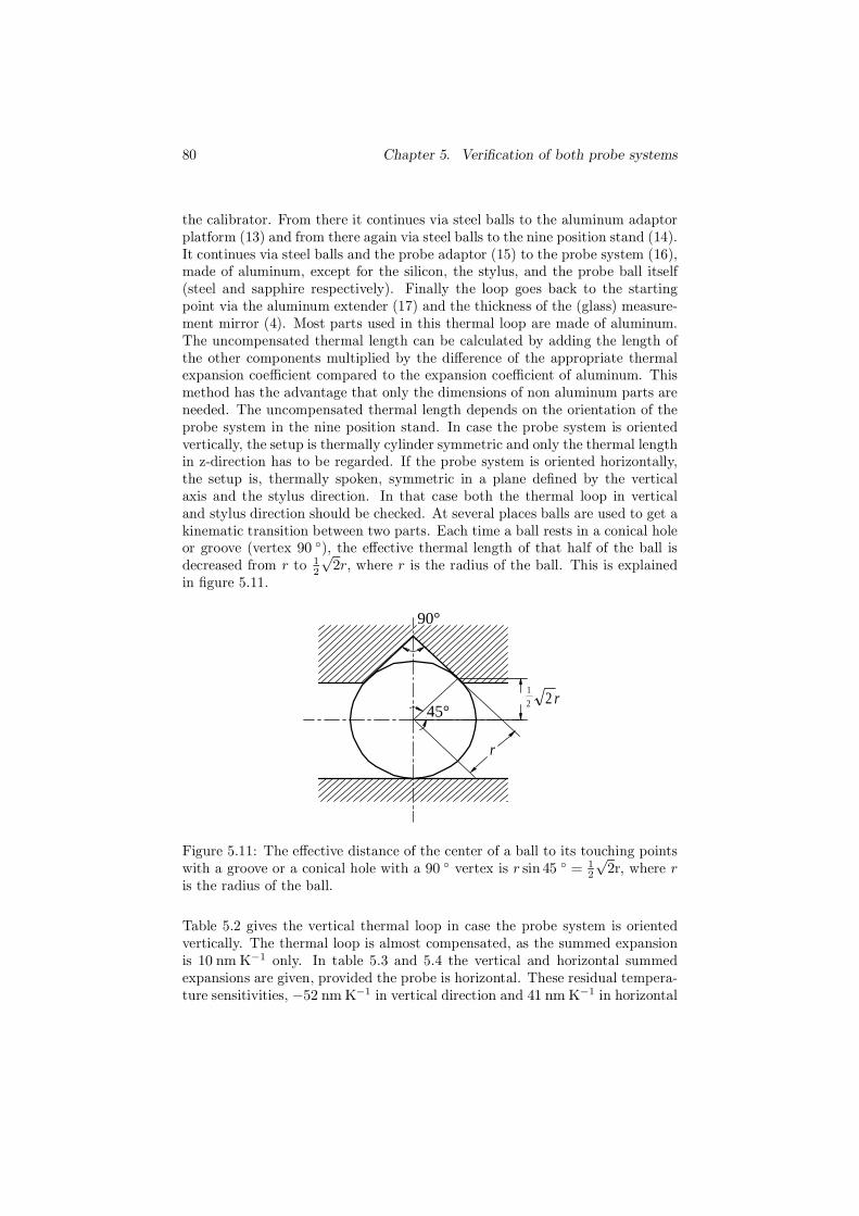
80 Chapter 5. Verification of both probe systems
the calibrator. From there it continues via steel balls to the aluminum adaptorplatform (13) and from there again via steel balls to the nine position stand (14).It continues via steel balls and the probe adaptor (15) to the probe system (16),made of aluminum, except for the silicon, the stylus, and the probe ball itself(steel and sapphire respectively). Finally the loop goes back to the startingpoint via the aluminum extender (17) and the thickness of the (glass) measure-ment mirror (4). Most parts used in this thermal loop are made of aluminum.The uncompensated thermal length can be calculated by adding the length ofthe other components multiplied by the difference of the appropriate thermalexpansion coefficient compared to the expansion coefficient of aluminum. Thismethod has the advantage that only the dimensions of non aluminum parts areneeded. The uncompensated thermal length depends on the orientation of theprobe system in the nine position stand. In case the probe system is orientedvertically, the setup is thermally cylinder symmetric and only the thermal lengthin z-direction has to be regarded. If the probe system is oriented horizontally,the setup is, thermally spoken, symmetric in a plane defined by the verticalaxis and the stylus direction. In that case both the thermal loop in verticaland stylus direction should be checked. At several places balls are used to get akinematic transition between two parts. Each time a ball rests in a conical holeor groove (vertex 90 ), the effective thermal length of that half of the ball isdecreased from r to 1
2
√2r, where r is the radius of the ball. This is explained
in figure 5.11.
45°
90°
12 2 r
r
Figure 5.11: The effective distance of the center of a ball to its touching pointswith a groove or a conical hole with a 90 vertex is r sin45 = 1
2
√2r, where r
is the radius of the ball.
Table 5.2 gives the vertical thermal loop in case the probe system is orientedvertically. The thermal loop is almost compensated, as the summed expansionis 10 nm K−1 only. In table 5.3 and 5.4 the vertical and horizontal summedexpansions are given, provided the probe is horizontal. These residual tempera-ture sensitivities, −52 nm K−1 in vertical direction and 41 nm K−1 in horizontal

5.1. Design of the calibrator 81
Vertical Thermal Loop, probe verticalmaterial αrel length expansion
in 10−6 K−1 in mm in nm K−1
ball between platforms steel 12-23=-11 7.07 -78
ball under nine position stand steel 12-23=-11 8.54 -94
ball under probe adapter steel 12-23=-11 7.07 -78
chip silicon 4-23=-19 0.4 8
stylus steel 10-23=-13 8 104
probe ball sapphire 4-23=-19 0.4 8
measurement mirror glass 8-23=-15 8 120
summed expansion -10
Table 5.2: Vertical Thermal Loop, probe vertical; αrel gives the expansiondifference between the specified material and aluminum. A minus sign in thelast column means that the probe tip is moved in negative z-direction.
Vertical Thermal Loop, probe horizontalmaterial αrel length expansion
in 10−6 K−1 in mm in nm K−1
ball between platforms steel 12-23=-11 7.07 -78
ball under nine position stand steel 12-23=-11 8.54 −94measurement mirror glass 8-23=-15 8 120
summed expansion -52
Table 5.3: Vertical Thermal Loop, probe horizontal; αrel gives the expansiondifference between the specified material and aluminum. A minus sign in thelast column means that the probe tip is moved in negative z-direction.
Horizontal Thermal Loop, probe horizontalmaterial αrel length expansion
in 10−6 K−1 in mm in nm K−1
ball under probe adapter steel 12-23=-11 7.07 -78
chip silicon 4-23=-19 0.4 8
stylus stainless steel 10-23=-13 8 104
probe ball sapphire 4-23=-19 0.4 8
summed expansion 41
Table 5.4: Horizontal Thermal Loop, probe horizontal; αrel gives the expansiondifference between the specified material and aluminum. A minus sign in thelast column means that the probe tip is moved in negative z-direction.

82 Chapter 5. Verification of both probe systems
direction, are higher compared to the vertical oriented probe system. For themaximally allowed temperature variation of 0.1 K, the thermal drift is hence5.2 nm. Because the time constant of the parts are not equal, e.g. compare thetiny stylus to the body of the calibrator, fast temperature variations should beprevented. This is assured by thermally insulating the calibrator from the sur-roundings by a four centimeter thick polystyrene box. In all measurements thetemperature is recorded. In practice, temperature variations within one hourwere typically less than 2mK, due to careful thermal isolation as explained insection 5.2.2. Since the maximum summed expansion is 52 nm K−1, the ex-pected thermal drift is 0.1 nm, much less than the worst case drift of 5.2 nm.Even the worst case thermal drift is well below the required uncertainty of10 nm.
Errors due to misalignment of the mechanics Misalignment of the probesystem relative to the motion direction of the calibrator causes errors propor-tional to the displacement. Mechanical tolerances in the order of a milliradianare reachable using standard manufacturing techniques. This leads to a relativeerror of 0.1%, which is acceptable. Since the uncertainty of the interferometersystem is only 1 nm, and the expected thermal worst case drift is 5.2 nm, thecomplete system will satisfy the specifications.
5.2 Verification of the piezo-resistive probesystem
The verification of the piezo-resistive probe system is carried out in several sep-arate experiments. First the electric behaviour of the probe system is checked.Then the displacements measurements using the calibrator described in theprevious section are presented. Finally the stability and repeatability are de-termined in a stability test.
5.2.1 Electric characterisation
The AC impedance of the strain gauge resistors has been tested as a functionof the frequency of the applied voltage. It turns out that there is a purelyresistive behaviour until about 40 kHz, as can be seen in figure 5.12. Above thisfrequency the impedance decreases and the phase retards, implying capacitivecoupling. A simple parallel RC circuit has been fitted to the data: R and Cvalues around 20 kΩ and 100 pF have been found.

5.2. Verification of the piezo-resistive probe system 83
100
101
102
103
104
105
104
105
impedanceim
peda
nce
/ O
hm
100
101
102
103
104
105
-0.5
0
0.5angle
angl
e / r
ad
frequency / Hz
Figure 5.12: Impedance and phase angle between two neighbouring testpoints(e.g. A and B in figure 2.12) of a Wheatstone bridge as function of the fre-quency. There is no obvious difference between the impedance shown here andimpedances between other neighbouring points of this bridge or other bridgesof the same device.
5.2.2 Displacements measurements
The displacements measurements consist of repeated back and forth movementsimposed to the probe, while recording the displacement, the imbalance of thebridges, and the temperature at about eight places. The direction of the move-ment is varied by changing the orientation of the probe system. These measure-ments serve to determine a number of parameters:
• the sensitivity of the imbalance of the bridges to probe displacements indifferent directions (i.e. the first order dependence),
• deviations from linear behaviour like second and higher order contribu-tions, reproducibility, and hysteresis,
• the change of the sensitivity in time due to random effects, quantified bythe standard deviation, and instability,
• the matrix A, transforming the measurement data to x-, y-, and z-displacements of the probe tip expressed in probe system co-ordinates.

84 Chapter 5. Verification of both probe systems
A can be determined knowing the sensitivity in at least three indepen-dent directions.
The measurement is executed in a polystyrene isolation box which effectivelyattenuates temperature fluctuations on a short and medium long time scale. Thelaboratory is known to have a 25 minutes periodic temperature fluctuation oftypically 0.1 K which is attenuated to milliKelvin level. The box also preventsair turbulence, which breaks up the homogeneity of the index of refraction.Different indices for the reference and measurement beam path of the laserinterferometer system result in a measurement error, as explained in section5.1.3.
The imbalance of the strain gauge bridges is measured at discrete points in a4 µm range. The distance between these points is typically 0.05 to 0.1 µm. Ateach point the imbalance of the bridges is measured 20 times; the average andthe standard deviation are computed and stored. This procedure takes about0.5 seconds. A measurement error could be induced if the probe position is notstable during this measurement and if the mirror position and the probe positionare not determined at the same time. The sign of this error changes when themoving direction of the actuated mirror changes causing a difference betweenback and forth measurement data, which suggests hysteresis. This effect isprevented by allowing the piezo to stabilize before a measurement is performed,by taking the average of two laser measurements performed before and afterthe imbalance of the bridges is measured, and by rejecting and repeating themeasurement if the difference between both laser measurements is more thanone nanometre.
Two successive back and forth measurements are executed. The next doubleback and forth measurement is performed after 15 or 60 minutes, depending onthe total duration of the measurement.
The probe system is oriented in one vertical orientation and three horizontalorientations, as explained in figure 5.13. This means that the probe is moved inthe directions (0,0,−1), (1,0,0), (− 1
2 ,− 12
√3,0), and (− 1
2 ,12
√3,0), expressed
in a frame fixed to the probe system. The residuals, i.e. the excitation of thebridges after subtracting the linear behaviour are shown in figure 5.14 to 5.17.To check for measurement errors, all measurements were repeated about oneweek later. The sensitivity of the bridges to displacement of the probe in acertain direction is shown in table 5.5 for both measurement sequences (markedmeas. 1 and meas. 2).
The A-matrix (transforming probe displacements to excitation levels of theWheatstone bridges) can be calculated using the sensitivities presented above.The sensitivities and the matching directions are conjugated points in theWheatstone bridge space and the probe translation space respectively: the di-rection vectors transform into sensitivities by applying A. This way a set oftwelve (three sensitivities times four directions) equations can be formulated,from which the nine components of theA-matrix can be solved by a least squares

5.2. Verification of the piezo-resistive probe system 85
Figure 5.13: This figure shows the four directions in which the probe systemis calibrated. Vertical probing at the left side, and three horizontal probingdirections at the right side. For the three horizontal probing setups the probesystem is mutualy rotated over 120 along the stylus. Below the plot of eachprobing direction, the probe system’s coordinate frame is given, as well as theprobing direction expressed in the probe system’s frame. The origin of eachframe is the intersection of the symmetry axis of the stylus and the plane throughthe slender rods. Utmost left, the frame of the calibrator is given.
probing direction sensitivity of the bridges in nVV−1nm−1
rod 1 rod 2 rod 3avg std avg std avg std
(0, 0,−1) meas. 1 455.7 0.20 391.0 0.22 339.2 0.42meas. 2 459.9 0.26 394.4 0.18 342.8 0.14(− 1
2 ,− 12
√3,0)
meas. 1 -84.6 0.12 -118.1 0.15 177.8 0.12meas. 2 -83.7 0.07 -117.7 0.12 179.3 0.12
(1, 0,0) meas. 1 244.8 0.49 -64.3 0.16 -97.1 0.30meas. 2 246.1 0.09 -63.8 0.08 -97.1 0.12(− 1
2, 12
√3,0)
meas. 1 -124.2 0.09 213.5 0.46 -55.0 0.30meas. 2 -124.5 0.63 213.2 0.72 -54.9 0.53
Table 5.5: Sensitivity of the Wheatstone bridges to displacement in differentprobing directions
method. Using the averaged sensitivities of the second measurement sequenceA is found to be:
Afit=
0.2334 −0.0235 −0.4577−0.0744 0.1912 −0.3948−0.1062 −0.1352 −0.3424
. (5.14)

86 Chapter 5. Verification of both probe systems
0 1 2 3 4-5
0
5
10
15
20
25re
sidu
al in
µV
/V
1
2
3
Figure 5.14: Residuals of the exitation of the bridges as function of the im-posed displacement in (0, 0,−1) direction after subtracting best fitting line.The rod number is indicated at the right side of the plot. The sensitivities ofthe bridges for the imposed translation, i.e. the slopes of the subtracted lines,are 0.4599, 0.3944,0.3428(µ V/ V)/ nm for rod 1, 2, and 3 respectively.
0 1 2 3 4-5
0
5
10
15
20
25
resi
dual
in µ
V/V
1
2
3
Figure 5.15: Residuals of the exitation of the bridges as function of the imposeddisplacement in (− 1
2,− 1
2
√3, 0) direction after subtracting best fitting line. The
rod number is indicated at the right side of the plot. The sensitivities of thebridges for the imposed translation, i.e. the slopes of the subtracted lines, are−0.0837, −0.1177, and 0.1793 (µ V/ V)/ nm for rod 1, 2, and 3 respectively.

5.2. Verification of the piezo-resistive probe system 87
0 1 2 3 4-5
0
5
10
15
20
25re
sidu
al in
µV
/V
1
2
3
Figure 5.16: Residuals of the exitation of the bridges as function of the im-posed displacement in (1,0,0) direction after subtracting best fitting line. Therod number is indicated at the right side of the plot. The sensitivities of thebridges for the imposed translation, i.e. the slopes of the subtracted lines, are0.2461,−0.0638,−0.0971(µ V/ V)/ nm for rod 1, 2, and 3 respectively.
0 1 2 3 4-5
0
5
10
15
20
25
resi
dual
in µ
V/V
1
2
3
Figure 5.17: Residuals of the exitation of the bridges as function of the imposeddisplacement in (− 1
2, 12
√3,0) direction after subtracting best fitting line. The
rod number is indicated at the right side of the plot. The sensitivities of thebridges for the imposed translation, i.e. the slopes of the subtracted lines, are−0.1245, 0.2132,−0.0549(µ V/ V)/ nm for rod 1, 2, and 3 respectively.

88 Chapter 5. Verification of both probe systems
Using Afit, new residuals can be calculated transforming the measured data toprobe displacements and subtracting the imposed translation. These residualsare called xyz-residuals to distinguish them from the residuals shown in figure5.14 to 5.17. The xyz-residuals are displayed in figure 5.18 to 5.21.
Discussion of the displacement measurements
A lot of data has been acquired by the displacement measurements. Moststriking are the large residuals, which will be discussed first.
Fitting of the A-matrix It is clear that the xyz-residuals suffer from someremaining linear error. Apparently it is not possible to fit a single A to all thedata. This can be made clear directly, without calculatingA, by considering thefollowing inconsistency in the data. Three horizontal measurements,
−→Xt1,
−→Xt2,
and−→Xt3, have been done, in the directions shown in figure 5.22. The imbalance
of the bridges has been measured to be−→M1,
−→M2, and
−→M3, respectively. It has
been assumed that there exists a matrix A which transfers−→Xt into
−→M for every
direction.−→Xt1,
−→Xt2, and
−→Xt3 have been chosen so that they add to zero (5.15).
−→Xt1 +
−→Xt2 +
−→Xt3 = 0 (5.15)
0 0.5 1 1.5 2 2.5 3 3.5 4-20
-10
0
10
20
30
40
50
displacement in µm
resid
ual
in n
m
z
y
x
Figure 5.18: Residuals in x-, y-, and z-directions, expressed in calibrator coor-dinates, of the probe being moved in (0,0,−1) direction (in probe coordinates).

5.2. Verification of the piezo-resistive probe system 89
0 0.5 1 1.5 2 2.5 3 3.5 4-20
0
20
40
60
80
100
120
140
160
displacement in µm
resid
ual
in n
m
z
y
x
Figure 5.19: Residuals in x-, y-, and z-directions, expressed in calibrator coor-dinates, of the probe being moved in (− 1
2 ,− 12
√3,0) direction (in probe coordi-
nates).
0 0.5 1 1.5 2 2.5 3 3.5 4-20
0
20
40
60
80
100
120
140
160
displacement in µm
resid
ual
in n
m
z
y
x
Figure 5.20: Residuals in x-, y-, and z-directions in calibrator coordinates ofthe probe being moved in (1,0, 0) direction (in probe coordinates).

90 Chapter 5. Verification of both probe systems
0 0.5 1 1.5 2 2.5 3 3.5 4-40
-20
0
20
40
60
80
100
120
140
160
displacement in µm
resid
ual
in n
m
z
y
x
Figure 5.21: Residuals in x-, y-, and z-directions in calibrator coordinates ofthe probe being moved in
(− 12, 12
√3, 0)direction (in probe coordinates).
1
2
3
t
t
t
x
y
XX
X
r
r
r
Figure 5.22: Three horizontal directions in which the sensitivity of the probesystem has been measured.
The sensitivities should also add to zero as proven in (5.16):
−→M1 +
−→M2 +
−→M3 =A
−→Xt1 +A
−→Xt2 +A
−→Xt3 =A
(−→Xt1 +
−→Xt2 +
−→Xt3
)= 0 (5.16)
However, this is not the case. In reality the three sensitivities add up to a vectoras if there would be a vertical displacement. This can be seen in table 5.6 wherethe sensitivities are scaled in order to be unity for a vertical displacement.Thesum of the horizontal sensitivities not being zero can only be explained if:
1.−→Xt1 +
−→Xt2 +
−→Xt3 = 0 due to imperfections of the calibration setup. These
imperfections include:

5.2. Verification of the piezo-resistive probe system 91
probing direction scaled sensitivity of the bridgesmeasurement 2 rod 1 rod 2 rod 3[0,0,−1] 1 1 1[− 1
2 ,− 12
√3, 0]
-0.1820 -0.2994 0.5230[1,0,0] 0.5351 -0.1618 -0.2832[− 1
2, 12
√3,0]
-0.2707 0.5406 -0.1602
sum over horizontal directions 0.0824 0.0794 0.0796
Table 5.6: Sensitivity of the Wheatstone bridges to displacement in differentprobing directions scaled to unity for the vertical direction. The sum of thescaled sensitivities of the horizontal directions gives a residual displacement inan almost pure vertical direction.
(a) the orientation of the probe system relative to the calibration plat-form is not according to specification,
(b) the calibrator movement is not perpendicular to the platform,
(c) the probe shifts over the surface.
2. The A-matrix is not constant because it depends on:
(a) probe orientation,
(b) probing direction.
There are some indications that the tip is shifting over the calibrator surface.However not all measurements can be explained. Appendix F discusses thispossibility extensively. It is also explained there why the other possibilities areless likely.
The best remedy for the problem mentioned above is to use a high accurateCMM instead of the calibrator. That will rule out the explanations 1a, 1b, and2a. Possibility 1c is best prevented by fixing all degrees of freedom of the tipduring the calibration. This can be done by forcing the tip to three spheres ofabout the same size as the tip, or by forcing it into the corner of a small sizehollow cube corner.
Comparison of the fitted and the theoretical A-matrix How does theA-matrix compare to theory? Answering this question is difficult due to thelarge number of uncertainties that have their influence on the A-matrix:
• Due to process variations not all bridges necessarily react equally to thesame displacement.
• The probe system may be rotated in the probe adapter, especially aroundthe probe’s z-axis.

92 Chapter 5. Verification of both probe systems
• The stylus may be tilted relative to the probe’s z-axis or may not gothrough the origin.
• The calibration procedure is probably not completely adequate given theproblems to fit a single A-matrix.
Both the fitted (5.14) and the theoretical (A.38) A-matrices are repeated here.The values given in table 4.2 are applied to (A.38).
Afit =
0.2334 −0.0235 −0.4577−0.0744 0.1912 −0.3948−0.1062 −0.1352 −0.3424
Atheory =
3tsGl
4l2s lst
4xs 4ys − 2ls 4lst−2xs − 2
√3ys +
√3ls 2
√3xs − 2ys + ls 4lst
−2xs + 2√
3ys −√
3ls −2√
3xs − 2ys + ls 4lst
= −6
0.2275 −0.0143 −0.3906−0.1013 0.2041 −0.3906−0.1261 −0.1898 −0.3906
(5.17)
Most striking is a factor of about −6 between the theoretical A and the fit-ted A, which has, for the reader’s convenience, been factorised from Atheory.Apparently the gauge factor Gl is considerably lower than specified in theory.No attempt has been made the find the cause of this low gauge factor. Theminus sign has no meaning except that the polarity of the bridges is reversed.Apart from this, the two matrices compare relatively well to each other giventhe number of unknowns.
Stability of the sensitivity and the A-matrix The stability of the sensi-tivities has already been given in table 5.5. It gives both a standard deviationbased on a moderately long measurement (ranging from 2 to 66 hours), as wellas a second measurement about one week later. The effect of these uncertain-ties on the A-matrix can be expressed in a variation matrix dA, which can becalculated in the same way as A. The variation of the calculated tip translation−−→dTpx can be expressed as:
−→M = (A+dA)
(−→Tpx +
−−→dTpx
)−→M = A
−→Tpx +dA
−→Tpx +A
−−→dTpx + dA
−−→dTpx
(A+dA)−−→dTpx = −dA−→Tpx−−→dTpx = − (A+dA)−1 dA
−→Tpx, (5.18)
where the fact that−→M = A
−→Tpx still holds is used. The maximum relative
error, being defined as∣∣∣−−→dTpx
∣∣∣/ ∣∣∣−→Tpx∣∣∣, equals the maximum singular value of

5.2. Verification of the piezo-resistive probe system 93
− (A+ dA)−1 dA. The proof of this is equivalent to the proof given in ap-pendix A equations (A.40) to (A.43). Calculating the maximum relative errorfor the second measurement given in table 5.5 gives 0.12%. For a 4 µm rangemeasurement the linearity error is maximally 4.8 nm, which is within specifica-tion.
Hysteresis, non-linearity, and reproducibility Hysteresis and non-linearity in directions other then the probing direction should be consideredwith care, because those kind of errors in other directions may be caused byshifting of the tip over the calibration surface. Non linearity has not been foundin any of the measurements. Hysteresis could not be detected in the 4 µmrange measurements, implying it is at least less than 10 nm. For the 25 µmrange measurements some hysteresis, up to about 20 nm can be seen. For mostaccurate measurements it is hence best to keep tip displacements small. Eachcalibration measurement consists of a number back and forth runs. In eachrun, each position is measured four times, two times forth and two times back.The reproducibility is calculated for each point and averaged over all pointsand runs. The result is given in table 5.7.Since each run is finished in about
probing direction Averaged reproducibilitymeasurement 2 x [nm] y [nm] z [nm](probe coordinates) (calibrator coordinates)[0,0,−1] 2.8 2.7 3.3[− 1
2,− 1
2
√3, 0]
1.5 2.2 6.3[1,0, 0] 2.1 2.9 5.0[− 1
2, 12
√3,0]
1.6 2.3 6.3
Table 5.7: One sigma reproducibility of the calibrations
ten minutes and the approaching direction is alternated for each measurementof a point, stability over maximally ten minutes, hysteresis, and repeatabilitycontribute to the reproducibility numbers in table 5.7.
stability In some of the residuals, e.g. in figure 5.19, a drift of up to 10 nmcan be seen. Stability, however, is better researched in a separate setup withoutactuator and measurement system. The next subsection deals with it.
5.2.3 Stability measurements
Stability measurements have been performed using a fixed distance setup inorder to reduce the number of possibly drifting elements. The setup consists ofa fixed height stand, the nine position stand and the probe itself (figure 5.23).The result of this measurement is shown in figure 5.24.
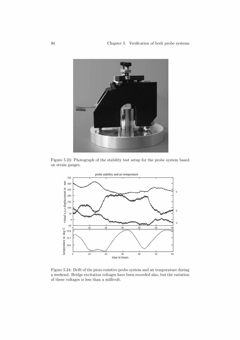
94 Chapter 5. Verification of both probe systems
Figure 5.23: Photograph of the stability test setup for the probe system basedon strain gauges.
0 10 20 30 40 50 60-50
0
50
100
150
200
250
300
350probe stability and air temperature
vir
tual
x,y
,z d
ispla
cem
ent
in n
m
x
y
z
0 10 20 30 40 50 60
19.6
19.7
19.8
time in hours
tem
per
ature
in
deg
C
Figure 5.24: Drift of the piezo resistive probe system and air temperature duringa weekend. Bridge excitation voltages have been recorded also, but the variationof these voltages is less than a millivolt.

5.2. Verification of the piezo-resistive probe system 95
Drift statistics for 60 (and 15) minute windowx (nm) y (nm) z (nm)
RMS drift 5.0 (3.1) 7.9 (4.1) 3.8 (1.5)maximum drift 16 (11) 30 (15) 12 (5.0)RMS error 4.0 (3.0) 5.8 (3.9) 2.7 (1.4)maximum error 18 (13) 30 (19) 14 (5.9)RMS drift compensated error 3.2 (3.1) 4.3 (4.0) 1.9 (1.4)maximum drift compensated error 16 (13) 20 (17) 8.0 (5.6)
Table 5.8: Drift data.
A few statistics have been calculated from the data presented in figure 5.24for different measurement times. The stability of this data seems considerable,but usually a measurement will be finished in a few minutes. For any period(window) in the time the measurement was taken, a drift and an error (1σvalue) can be calculated. The drifts and errors for all possible 60 and 15 minutewindows have been calculated. In table 5.8 the standard deviation and themaximum value (i.e. worst case) of all these drifts and errors are shown for a 60and a 15 minute window. The 15 minute window data is given in parentheses.Two measurement strategies can be used. In the first one the origin of theworkpiece is measured once and all measured points are calculated relative tothis origin. In order to reduce the effect of drift, the origin can be measuredagain at the end of the measurement sequence. The drift can be estimated atany time in the measurement sequence by linearly interpolating between thetwo origins. In this way the individual measurement points can be correctedfor drift. The drift corrected RMS and maximum errors are also mentioned intable 5.8.
5.2.4 Discussion of the stability data
The stability measurements show that the probe system suffers from a consider-able drift requiring frequent rezeroing for the highest accuracy. The drift couldbe caused by a varying parasitic resistance between the connection pads andthe silicon substrate. Earlier measurements showed comparable but even largerdrifts. Careful bonding using less energy decreased the problem to the presentlevel. It is well possible that the effect is still present and can only be solvedcompletely by increasing the thickness of the isolating layer between the bondpads and the substrate (which is now 250 nm). There are two more argumentsfor this statement. First, interchanging the supply pins and the measurementpins of the Wheatstone bridges can have a large effect on the stability. This canbe explained by the parasitic resistance hypothesis if some but not all bondingpads have a resistive coupling to the substrate. Only parasitic resistances atone of the measurement pins will degrade the stability of the probe system.Second, the stability of the raw bridge signals before applying A is not equal

96 Chapter 5. Verification of both probe systems
0 10 20 30 40 50 60-20
0
20
40
60
80
100
120
140probe system stability per bridge
time in hour
chan
ge
of
imbal
ance
of
the
bri
dges
in µ
V/V
rod 1
rod 2
rod 3
Figure 5.25: Stability of the individual bridges.
for all bridges. Rod 1 is behaving better than the other rods, as can be seen infigure 5.25.
It is also possible that the piezo-resistors themselves drift. In that case themanufacturing process may lead to improvement. This will be a laborious andexpensive exercise. Such a path has probably been followed to improve piezoresistive pressure and acceleration sensors, but the results are for the larger partnot public.
The stability data can also be used to determine the repeatability. Five min-utes is taken as a reasonable threshold between stability and repeatable. Thisimplies that all signals with a frequency higher than 1
300Hz are assumed to be
repeatability. Hence the data is to be high-pass filtered, for which a 1300 Hz
fourth order Butterworth filter is used. The standard deviation of the filteredsignal is 1.7 nm in x-direction, 2.1 nm in y-direction, and 0.7 nm in z-direction.
In conclusion, the probe system performs according to specification apart fromthe stability. The repeatability and hysteresis are low, the linearity is good.The worst case instability of 30 nm can be overcome by doing the most accuratemeasurements in a 15 minute time span or by more frequent re-zeroing. Thecalibration problems that showed up using the 1D calibrator will probably notoccur when using a high accuracy CMM and a hollow corner cube to preventshifting of the probe tip.

5.3. Verification of the optical probe system 97
5.3 Verification of the optical probe system
Like the piezo-resistive probe system, the optical probe system is tested indifferent setups for sensitivity effects and drift effects. Due to time limitationsno special stand has been made: a standard stand has been used, which rests onthe optical bench, next to the calibrator. This decision has a few consequences.First the thermal loop is long and drift is expected. Second the stand used canonly hold the probe system in vertical direction. It is therefore impossible tocheck the system in horizontal directions. As the probe system is optimisedfor use in vertical direction, relatively large errors are expected for horizontalprobing which would probably make it impossible to draw conclusions.
5.3.1 Displacement measurements
Early displacement measurements have been done using a calibrator borrowedfrom the Dutch Metrology Institute (NMi), because the calibrator described inthis thesis was not finished at that time. The NMi calibrator is actuated bya piezo with accurate capacitive feedback. The capacitive sensor is calibratedperiodically by a Fabry Perot cavity which can be added on top of the calibra-tor. The system is described by Haitjema [Haitjema 98]. In order to distinguishbetween displacements and drift, the calibrator is sent back to its starting posi-tion between every point in the measurement. This way it is possible to log thedrift during the measurement and subtract it from the data. A displacementmeasurement over about 10 micrometre is presented in figure 5.26. This resultwas published before [Pril 97]. The residual is calculated by subtracting a bestfitting line as well as a best fitting third order polynomial. Both are shown infigure 5.27. From the left side of this plot it can be concluded that non-linearterms should be taken into account for this range. This is why the right sideshows the residual after subtracting a best fitting third order polynomial. Whatremains is mainly a periodic effect repeating every 390 nm, clearly caused by in-terference somewhere in the LDGU as the repetition length matches to half thewavelength of the laser light used (780 nm). Investigating where the interferencecould possibly occur, two places where found:
1. interference at the photo diodes by some unintended reflection somewherein the probe system,
2. back scattering into the laser diode. The mirror, of which the positionis to be measured, can form a second laser cavity together with the backside mirror of the laser diode. This will disturb the wave length stabilityof the laser. Via the chromatic aberration of the lenses (see appendix Band C) this can cause measurement errors.
A quick experiment was done to distinguish between these two possibilities.An uncoated glass plate, which reflects about four percent of the light, was
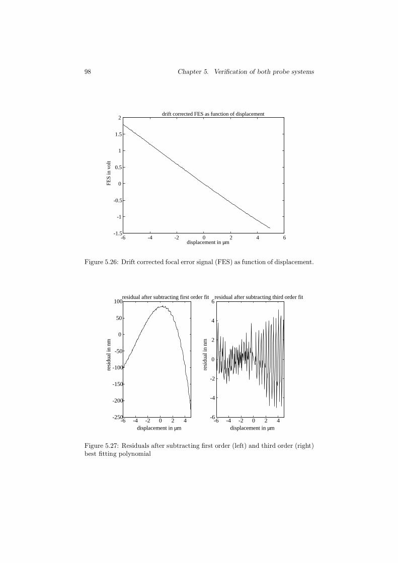
98 Chapter 5. Verification of both probe systems
-6 -4 -2 0 2 4 6-1.5
-1
-0.5
0
0.5
1
1.5
2drift corrected FES as function of displacement
displacement in µm
FES
in v
olt
Figure 5.26: Drift corrected focal error signal (FES) as function of displacement.
-6 -4 -2 0 2 4-250
-200
-150
-100
-50
0
50
100residual after subtracting first order fit
displacement in µm
resi
dual
in n
m
-6 -4 -2 0 2 4-6
-4
-2
0
2
4
6residual after subtracting third order fit
displacement in µm
resi
dual
in n
m
Figure 5.27: Residuals after subtracting first order (left) and third order (right)best fitting polynomial
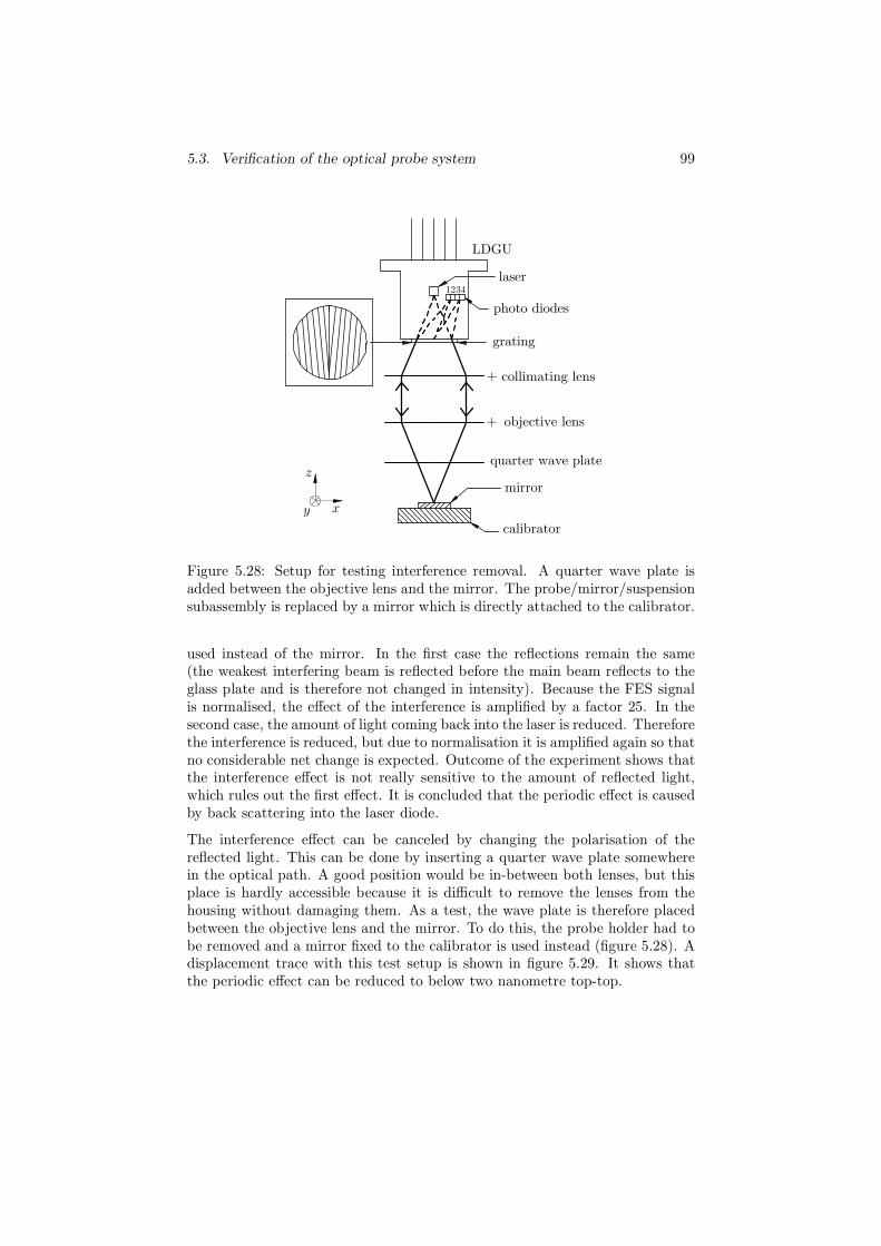
5.3. Verification of the optical probe system 99
LDGU
laser
photo diodes
grating
collimating lens
objective lens
quarter wave plate
mirror
calibrator
x
z
y
+
+
1234
Figure 5.28: Setup for testing interference removal. A quarter wave plate isadded between the objective lens and the mirror. The probe/mirror/suspensionsubassembly is replaced by a mirror which is directly attached to the calibrator.
used instead of the mirror. In the first case the reflections remain the same(the weakest interfering beam is reflected before the main beam reflects to theglass plate and is therefore not changed in intensity). Because the FES signalis normalised, the effect of the interference is amplified by a factor 25. In thesecond case, the amount of light coming back into the laser is reduced. Thereforethe interference is reduced, but due to normalisation it is amplified again so thatno considerable net change is expected. Outcome of the experiment shows thatthe interference effect is not really sensitive to the amount of reflected light,which rules out the first effect. It is concluded that the periodic effect is causedby back scattering into the laser diode.
The interference effect can be canceled by changing the polarisation of thereflected light. This can be done by inserting a quarter wave plate somewherein the optical path. A good position would be in-between both lenses, but thisplace is hardly accessible because it is difficult to remove the lenses from thehousing without damaging them. As a test, the wave plate is therefore placedbetween the objective lens and the mirror. To do this, the probe holder had tobe removed and a mirror fixed to the calibrator is used instead (figure 5.28). Adisplacement trace with this test setup is shown in figure 5.29. It shows thatthe periodic effect can be reduced to below two nanometre top-top.

100 Chapter 5. Verification of both probe systems
0 0.5 1 1.5 2 2.5 3 3.5 4-1
-0.8
-0.6
-0.4
-0.2
0
0.2
0.4
0.6
0.8residuals with quarter waveplate
displacement in µm
resi
dual
in n
m
Figure 5.29: Residual after subtracting a third order best fitting polynomialfor an LDGU based probe system equiped with a quarter wave plate. Theinterference effect is reduced to a band of less than two nanometre, comparedto ten nanometre without waveplate.
5.3.2 Stability measurements
The displacements measurements described before were drift corrected, whichalso implies that drift in the sensor is removed. Stability of the probe systemis therefore checked in a different setup with a minimised thermal loop. Forthis purpose the probe/mirror/suspension subassembly is removed and replacedby a mirror fixed to the probe house. This way the stability of the probe’smeasurement system can be investigated. Mechanical stability of the probe andthe housing (in a real case the probe system will be attached to the CMM at thetop side) is not incorporated in this measurement. They can be calculated, basedon the thermal expansion of the materials, and added to the sensor stability.The FES signal was logged during almost five days. The result is given in figure5.30.
In a normal situation the probe is used for maximally one hour. Maximum driftobserved in one hour in figure 5.30 is 22 nm, but this drift occurred while therewas something wrong with temperature conditioning. After 40 hours, when thetemperature remains in its specified 0.1 K range, the maximum observed insta-bility is 8 nm. Excluding the part of the measurement where the temperature isout of specification, the typical drift per hour (one sigma) is 4 nm. The drift ispartly temperature related. When the temperature is fitted to the drift, a pro-portionality factor of 120 nm K−1 is found, which is substantially better than

5.3. Verification of the optical probe system 101
0 20 40 60 80 100 120
-250
-200
-150
-100
-50
0
drift measurement optical probe system
dri
ft i
n n
m
0 20 40 60 80 100 12020
20.5
21
21.5
time in hours
tem
per
atu
re i
n d
egre
e C
Figure 5.30: Stability measurement of the optical probe system. The tempera-ture during the measurement is also shown.
calculated. Possibly the achromatism of the lenses was less than specified. Thedata can also be used to determine the repeatability. Like the stability dataof the strain gauge based probe system, five minutes is taken as a reasonablethreshold between instability and repeatability. The standard deviation of thesignal filtered by a 1
300 Hz fourth order high pass Butterworth filter is 0.14 nm.
5.3.3 Discussion of the verification of the optical probe
system
This probe system behaves within specification. The largest error source isinstability with 8 nm worst case and 4 nm typical. The main part of the driftis probably caused by the heat produced by the laser diode itself, either viamechanical expansion or via a frequency shift of the laser. This is worked outin the error analysis in appendix C. Active cooling by Peltier elements maydecrease the drift further. The probe system’s repeatability is excellent with0.14 nm (1 sigma). A third order polynomial fit is needed to handle the non-linearities of the system. With nowadays computers and a CMM that can beused for easy calibration that should not be a problem. Hysteresis is neitherexpected nor detected.

102 Chapter 5. Verification of both probe systems
5.4 Summary
In this chapter the verification of both designed probe systems to the specifica-tions is described. In order to measure sensitivity to displacement, hysteresis,and non-linearity, a new calibration setup, the calibrator, has been designed andmanufactured. It enables the calibration of probes in one direction to 10 nmuncertainty with a 1 nm resolution. The design is based on a plane mirror dif-ferential interferometer, due to which the thermal loop can be kept very short.The use of the calibrator is not restricted to the calibration of the probe systemsdescribed in this thesis: It is a general purpose instrument, which can be, andhas been, used for the calibration of a wide range of sensors. Due to its highnatural frequency and the small response time of the interferometer system, itcan even be used for the calibration of roughness sensors, where a characteristicroughness profile is imitated by the piezo actuator. Traceability to the standardof length is secured via the use of a calibrated interferometer system.
For the probe system based on strain gauges the following characteristics havebeen measured:
• hysteresis: smaller than 10 nm (worst case) for 4 µm moves and smallerthan 20 nm for 25 µm moves
• reproducibility: smaller than 6 nm where individual data points are mea-sured with different scan directions and at different times
• instability of the sensitivity: 0.12%
• repeatability: 2 nm in x- and y-direction and 0.7 nm in z-direction
• instability: 30 nm worst case and 8 nm typical (one sigma) in a 60 hourmeasurement.
The LDGU based probe system is verified in z-direction only. The worst caseinstability is measured to be 8 nm in a 120 hour measurement. The typical (onesigma) instability is 4 nm. The one sigma repeatability is 0.14 nm. Hysteresishas not been detected. A third order polynomial fit is needed to get the residualsbelow 2 nm (top-top in a 4 µm range).
Summarising it can be stated both probe systems meet the requirements witha single exception: For highest accuracy, measurements with the probe systembased on strain gauges should be finished within 15 minutes.

Chapter 6
Conclusions and
recommendations
6.1 Conclusions
In this thesis the development of two probe systems with nanometre uncertaintyfor use on CMM’s is described. Furthermore, the design of a calibration systemthat was used for the majority of the described probe system qualifications ispresented. Based on the results, obtained with the two prototype probe systemsand the calibration setup, some conclusions can be drawn.
One of the requirements states that it should be possible to use small probetips without damaging the workpiece that is measured. Theory shows that thisrequires the probe system’s suspended mass to be smaller than 20 mg, and thesuspension to be compliant enough. Assuming some reasonable numbers for theCMM on which the probe system will be used, it has been shown that a stiffnessof 200 N m−1 is sufficiently low. Both probe systems satisfy these requirements.
A suspension that can fulfil both of the above stated requirements has beenused. It consists of three slender rods as elastic elements that enable motion ofthe probe tip in z-direction and pseudo translation in x- and y-direction. Theremaining degrees of freedom are fixed. All slender rods lie in one plane, whichenables easy manufacturing by etching. Both developed probe systems use thiskind of suspension, although the size and material of the suspensions are notthe same. Different measurement systems are used to measure a displacementof the tip.
The first probe system that was designed uses a 2D optical measurement systemthat is based on a sensor used in CD players. Although the system can inprinciple measure two DOF’s, it is optimised for measurement of z-translationof the probe tip. No measurements in the other direction have been performed.
103

104 Chapter 6. Conclusions and recommendations
Measurements showed that the probe system has a one sigma repeatability of0.14 nm. The instability is on average 4 nm per hour, but can have peaks of8 nm per hour, where the part of the measurements where the temperaturestability was out of specification has been left out. The drift is probably causedby the power dissipation in the laser diode in the sensor, not withstanding thespecial attention that has been paid to conduct the heat out of the structure.Theoretical error analysis showed that temperature fluctuations can cause errorsboth via the thermal loop as well as via the frequency stability of the laser diode,which causes measurement errors due to the achromatism of the lenses used. Anexperimental temperature sensitivity of 120 nm K−1 was found. The sensor hasa non-linear response to translation; a third order polynomial is used to reachresiduals of less than ±1 nm over a 4 µm range. Hysteresis was not detected,which implies it must be smaller than 1 nm.
The first probe system can only perform accurate measurements in one direc-tion. For actual use in a CMM three dimensional measurements are needed.Rather than expanding the measurement system of the first probe system withtwo additional measurement axes, it has been decided to develop a completelydifferent probe system based on strain gauges. Using micro system technology,the suspension can be made together with the strain gauges and their electri-cal connections on a silicon substrate. This probe system has some importantadvantages over the first design: The measurement system does not increasethe suspended mass and it requires few additional space. The mechanical con-struction is less complicated which will probably lead to cost benefits in seriesproduction. Disadvantages are the higher prototyping costs and the brittle-ness and anisotropy of the monocrystalline silicon that is used for the elasticelements.
Experimental verification showed that, like the first system, instability is thelimiting factor to the uncertainty. A worst case drift of 30 nm per hour hasbeen detected, while average drift is 8 nm. The drift may have been causedby a rather thin isolating layer between the bond pads and the substrate. Inthe first series of prototypes careful bonding with low energy cured part of aneven larger stability problem, but another part of the same problem may stillbe present. The gauge factor was found to be about a factor of six smaller thanclaimed in literature. This may also be part of the drift problem. Improvingthe gauge factor will also benefit the repeatability, which has now measured tobe 0.7 to 2.1 nm, depending on the probing direction. The relative uncertaintyis 0.12%. Hysteresis in the 4 µm calibration scans was smaller than 10 nm. The25 µm scans show a hysteresis of up to 20 nm. Reproducibility over two backand forth scans performed in ten minutes is 6 nm or less. Full 3D calibrationof the probe system could not be performed, probably because the probe shiftsover the measured surface. Preventing this shift and use of an accurate CMMis expected to solve this issue. Summarising the experimental verification of thestrain gauge based probe system, it can be concluded that the system meets allits specifications except for the instability, which implies that a measurementshould be finished in 15 minutes instead of one hour.

6.2. Recommendations 105
To verify both probe systems, an easy to use general purpose calibration setuphas been designed, based on a commercially available interferometer system.Theoretical error analysis and experiments show that the setup meets the un-certainty specification of 10 nm. If it is used in an environment that is betterconditioned than the specified 100mK, as was the case for the verifications pre-sented in this thesis, the uncertainty will even be considerably less than 10 nm.Also the repeatability meets the specified 1 nm. A matrix model was used toanalyse the effects of mirror unflatness and tilt on the interferometer system.This technique provides an efficient way to perform this kind of analysis and itis also applicable on other interferometer setups.
6.2 Recommendations
There is always room for improvement. Ideas that could not be brought in topractice due to time limitations, because critical tools were not (yet) available,or because it would require a new prototype, are presented here.
Although the design of the first probe system with the optical measurementsystem was not completed to a full 3D version in favour of the second, straingauge based probe system, a change of side conditions could make it the mostpromising approach again. In that case the measurement system should beexpanded by two extra axes. Although not presented in this thesis, plans weremade to use one of the first order beams, diffracting from the grating on thefirst path of the light, to measure tilt of the mirror in a triangulation setup likegiven in figure 2.9. Two mirrors and one lens would be needed to shape thebeam and send it, via the mirror attached to the probe, to a PSD or a fourquadrant photo diode. Those extra optics would make the probe house widerand difficult to manufacture. It may be better to adapt the LDGU to measurethree directions. This would require a change of the grating in order to split thebeam in four instead of in two. Eight photo diodes are needed to detect bothx, y, and z. Y can then be detected in the same way as x is detected in theoriginal LDGU. Probably some sensitivity in z-direction should be sacrificed infavour of the sensitivity in the two horizontal directions, probably by increasingthe focal length of the objective lens. The repeatability in z-direction is lowenough to do this, but the drift needs to be improved. Improvement is neededanyway, but the reduced sensitivity will degrade the stability: the thermal pathwill be longer due to the increased focal length of the collimator lens, and,according to (C.11), the sensitivity to achromatic aberration will increase. Bestsolution would be to remove the heat source and fiber deliver the light from adistant source. Pointing stability of light emitted by the fiber is an issue here.Van Vliet measured in his probe system a sensitivity to motion of the fibers[Vliet 96]. Alternatively the heat removal can be improved via active coolingby Peltier elements. A quarter wave plate should be used to attenuate periodiceffects due to back scattering in the laser diode.

106 Chapter 6. Conclusions and recommendations
The second probe system, based on strain gauges, is the first 3D CMM proberealised using MST. Being a first prototype, the results are promising. Never-theless, a few modifications would, retrospectively, have improved the system.Most of them deal with the rather high drift of the resistors of the Wheatstonebridges.
• Increase the thickness of the isolation layer between the bond pads andthe silicon substrate. This was found to be a problem in the past, causingexcessive drift. Careful bonding cured it to a more acceptable level, butit may still be part of the cause of the remaining drift.
• Provide a way to connect the silicon substrate to half the supply voltageof the Wheatstone bridges, or to ground, if the bridges are supplied sym-metrically. In case there is a residual resistance between the substrate andthe Wheatstone bridges the effect of this resistance will be significantlyreduced.
• Investigate whether a metal can be used as substrate (of which the elastichinges are made). This would prevent problems with the brittleness andanisotropy of silicon.
Both probe systems have been characterised using the newly designed 1D cali-bration setup. This instrument works fine for 1D measurements: the sensitivity,non-linearity, and hysteresis of the probe systems were determined accurately.It was planned to perform a full 3D calibration on the 1D calibration setupalso, but this partially failed, probably because the tip shifted over the surfaceof the calibrator extender bar. At the time the probe systems were validated,no CMM with sufficient accuracy was available. In the mean time, two highprecision CMM’s were realised. Rather than trying to find why the 3D calibra-tion on the calibrator was not successful, it is recommended to install the probesystem on one of the new CMM’s and do the 3D calibration there. This can bepart of a logical continuation of the project where the probe system should beintegrated with a high precision CMM anyway. Sliding of the tip can best beprevented by forcing the tip into a corner of a hollow cube. Movements in atleast three independent directions will calibrate the probe system in the sameway as presented in this thesis, but without reorientation of the probe system.
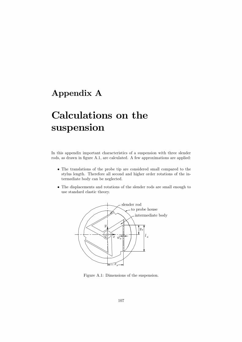
Appendix A
Calculations on the
suspension
In this appendix important characteristics of a suspension with three slenderrods, as drawn in figure A.1, are calculated. A few approximations are applied:
• The translations of the probe tip are considered small compared to thestylus length. Therefore all second and higher order rotations of the in-termediate body can be neglected.
• The displacements and rotations of the slender rods are small enough touse standard elastic theory.
x
w
y
lxz
s
s
s
s
y
slender rodto probe house
intermediate body
Figure A.1: Dimensions of the suspension.
107

108 Appendix A. Calculations on the suspension
• The effective length of a slender rod decreases when it is deformed outsidethe plane. The displacements are assumed to be small enough to neglectthis effect. If necessary the result can be corrected afterwards.
• All parts except the slender rods are assumed to be infinitely stiff.
The working out and solving of the equations given below is rather laboriousand can best be done using a symbolic mathematical software package.
The following definitions and conventions are used in this appendix:
• The z-axis is the symmetry axis of the suspension and the y-axis is parallelto the length direction of rod 1, like the co-ordinate frame given in figureA.1. Rods 2 and 3 are rotated over 120 and 240 degrees respectively.
• The subscript s is used to indicate a slender rod parameter.
• The subscript i is used to indicate a intermediate body parameter.
• The subscript t is used to indicate a probe tip parameter.
• The subscript n is used as an index n = 1..3 to label the three slenderrods.
• −→X is used to indicate a 3D translation.
• −→R is used to indicate a 3D rotation.
• −→D is a 6D vector composed of a 3D translation and a 3D rotation.
• −→P is used to indicate a 3D rest position.
• G is a 6D vector composed of a 3D force and a 3D moment.
A.1 Stiffness of the suspension
A.1.1 Stiffness of a slender rod
Consider rod 1 with length ls, width ws, thickness ts, and Young’s modulus Es.Its general stiffness matrix Cs1 can be defined as [Przemieniecki 68]:
Cs1 ≡
csxx csxy csxz cksxx cksxy cksxzcsxy csyy csyz cksyx cksyy cksyzcsxz csyz cszz ckszx ckszy ckszzcksxx cksxy cksxz ksxx ksxy ksxzcksyx cksyy cksyz ksxy ksyy ksyzckszx ckszy ckszz ksxz ksyz kszz
(A.1)

A.1. Stiffness of the suspension 109
Cs1 can be used to calculate the forces and moments working on the free endof the slender rod for a given displacement of the free end of the rod (as isdone in (A.8)). The elements cslm (l,m = x, y, z), expressed in Newton per me-tre, describe the resulting force for a certain displacement. The elements ckslm(l,m = x, y, z), expressed in Newton metre, describe the resulting moment fora certain rotation. The elements kslm (l,m = x, y, z), expressed in Newton,describe the force as a result of a rotation or the moment as a result of a trans-lation. The constants mentioned in Cs1 can be calculated using standard elastictheory. They can be found, among others, in Przemieniecki [Przemieniecki 68](except ksyy which was found in Young [Young 89]). All constants not men-tioned below are zero.
csxx =Estsw
3s
l3s
csyy =Estsws
ls
cszz =Est
3sws
l3s
cksxz = 12
Esw3sts
l2s(A.2)
ckszx = − 12
Eswst3s
l2s
ksxx = 13
Eswst3s
ls
ksyy ≈ Gswst3s
ls
(1
3− 0.21
tsws
(1− 1
12
t4sw4s
))kszz = 1
3
Esw3sts
ls
where Gs is the sliding modulus, equal to12Es(1 + νs)−1, with νs the Poisson
ratio. Note that Cs1 is symmetric. The stiffness matrices for rod 2 and 3 canbe calculated by rotating Cs1 over 120 and 240 degrees:
Cs2 =
(R120 ∅∅ R120
)Cs1
(R120 ∅∅ R120
)−1(A.3)
Cs3 =
(R120 ∅∅ R120
)2Cs1
(R120 ∅∅ R120
)−2, (A.4)
where R120 is a matrix rotating a point over 120 degrees around the z-axis.

110 Appendix A. Calculations on the suspension
A.1.2 Calculation of forces and moments
The intermediate body is connected to three equal slender rods s1, s2, and s3,at positions Ps1, Ps2, and Ps3, respectively. Ps1 is defined as:
Ps1 ≡ xs
ys0
. (A.5)
Ps2 and Ps3 can be calculated by rotating Ps1 over 120 and 240 degrees aroundthe z-axis respectively.
When a force Ft is applied to the probe tip at position Pt, the intermediatebody will translate over Xi and rotate over Ri (gathered together in Di):
Ft =
FtxFtyFtz
Pt =
PtxPtyPtz
=
00−lst
(A.6)
Di =
(Xi
Ri
)=
Xix
Xiy
Xiz
Rix
Riy
Riz
,
where lst is the stylus length. If other probes are applied, the more generalexpression for Pt should be used. Due to the translation and rotation of theintermediate body, the free ends of the rods will be displaced over Ds:
Dsn =
(Xi + Ri ∗ Psn
Ri
), n = 1..3. (A.7)
The forces Fsn and moments Msn acting on the rods, gathered together in Gsn,can be calculated by multiplying Dsn by Csn:
Gsn ≡(
FsnMsn
)=Csn Dsn, n = 1..3. (A.8)
Now all forces and moments acting on the intermediate body are in principleknown. Assuming a static situation the sum of the forces and the sum of themoments should equal zero:
Ft +3∑
n=1
− Fsn = 0
Pt ∗ Ft +3∑
n=1
(− Msn + Psn ∗ −Fsn
)= 0. (A.9)

A.2. Stresses in the slender rods 111
By solving these equations, the rotations and translations of the intermediatebody can be written as function of the applied force on the probe tip:
Di =1
3
2Ftx(csxx + csyy
)−12Fty
(csxx + csyy
)−1Ftz (cszz )
−1
−2lstFty(ksxx + ksyy + cszzx
2s + 2ckszxys + cszzy
2s
)−12lstFtx
(ksxx + ksyy + cszzx
2s + 2ckszxys + cszzy
2s
)−10
. (A.10)
Note that csyy is at least two orders of magnitude larger than the other cs-constants because ls is at least (by definition) one order of magnitude largerthan ts. This means that a displacement of the tip due to a translation of theintermediate body in x- or y-direction is two orders of magnitude smaller thana displacement of the tip due to a rotation of the intermediate body. Neglectingdisplacements of the intermediate body in x- and y- directions the applied forceon the tip can be written as function of the tip displacement Xt as:
Ft =
32
(ksxx + ksyy + cszzx
2s + 2ckszxys + cszzy
2s
)l−2st Xtx
32
(ksxx + ksyy + cszzx
2s + 2ckszxys + cszzy
2s
)l−2st Xty
3cszzXtz
≡
cxy ∅cxy
∅ cz
Xt (A.11)
where the sensed stiffnesses of the probe tip in xy-directions cxy and z directioncz are introduced. They can be expressed in stylus length, rod dimensions, andmaterial properties as:
cxy =3
2
Eswst3s
lsl2st
(A.12)(1
2 (1 + νs)
(1
3− 0.21
(tsws− 1
12
t5sw5s
))− ys
ls+
y2sl2s
+x2sl2s
+1
3
)cz = 3
Eswst3s
l3s. (A.13)
With this result the stiffness of the suspension sensed at the probe tip is calcu-lated. Note that the magnitude of the force is independent from the directionof the probe translation in the xy-plane.
A.2 Stresses in the slender rods
In this section the calculation of the stresses in the slender rods is explained.It is assumed that the slender rods are infinitely stiff in their length direction
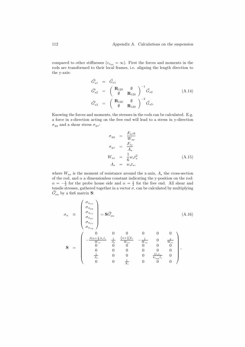
112 Appendix A. Calculations on the suspension
compared to other stiffnesses (csyy = ∞). First the forces and moments in therods are transformed to their local frames, i.e. aligning the length direction tothe y-axis:
G′
s1 = Gs1
G′
s2 =
(R120 ∅∅ R120
)−1Gs2 (A.14)
G′
s3 =
(R120 ∅∅ R120
)−2Gs3.
Knowing the forces and moments, the stresses in the rods can be calculated. E.g.a force in z-direction acting on the free end will lead to a stress in y-directionσyy and a shear stress σyz:
σyy =Ftzα
Wsx
σyz =FtzAs
Wsx =1
6wst
2s (A.15)
As = wsts,
where Wsx is the moment of resistance around the x-axis, As the cross-sectionof the rod, and α a dimensionless constant indicating the y-position on the rod:α = − 1
2 for the probe house side and α = 12 for the free end. All shear and
tensile stresses, gathered together in a vector σ, can be calculated by multiplyingG′
sn by a 6x6 matrix S:
σn ≡
σnxxσnyyσnzzσnyzσnxzσnxy
= SG′
sn (A.16)
S =
0 0 0 0 0 0
−β(α+ 1
2)tsls
Wsz
1As
(α+ 1
2)lsWsx
− 1Wsx
0 xWsz
0 0 0 0 0 00 0 0 0 0 01As
0 0 0 Gstsksyy ls
0
0 0 1As
0 0 0
,

A.3. Admissable overtravel computation 113
where Wsz is the moment of resistance around the z-axis, and β a parameterlike α for the z-direction. The result is worked out here for the first rod only:
σ1 =ts
2l3slst
0
Es (−12αxsXtx + (6αls − 12αys − ls)Xty − 12αlstXtz)00
−2Gsl2sXtx
−Ests (−2xslsXtx + (ls − 2ys)Xty − 2lstXtz)
.
(A.17)
A.3 Admissable overtravel computation
At a certain tip displacement the stresses in one of the rods will exceed a criticallimit. At this point a comparative von Mises stress σi will exceed the yield stressσY . σi is defined as [Dubbel 81]:
σ2i ≡ σ2 + 3τ2 ≡ σ2xx + σ2yy + σ2zz + 3(σ2yz + σ2xz + σ2xy
). (A.18)
The aim of this section is to calculate the smallest Xt that will increase thislimit. There is a direction for which rod 1 will break or plastically deform first.Because of symmetry there will be three smallest, but equally long Xt, eachincreasing the limit in one of the rods. It therefore satisfies to compare thecomparative stress to the yield stress for rod one only.
The matrix S is split up in two individual matrixes St and Ss for the calculationof the tensile stress and the shear stress:
S ≡(StSs
)(A.19)
σ1 = St G′
s1
τ1 = Ss G′
s1. (A.20)
Now the comparative von Mises stress can be calculated by:
σ2i ≡ σ21 + 3τ21 = σT1 σ1 + 3τT1 τ1 = G′Ts1
(STt St + 3STs Ss
)G′
s1. (A.21)
We want to relate σ2i to tip displacements Xt so G′
s1 should be expressed in tipdisplacements:
G′
s1 = Gs1 =Cs1 Ds1 =Cs1Q Xt, (A.22)
where
Q ≡ 1
lst
0 0 00 0 0xs ys lst0 1 0−1 0 00 0 0
. (A.23)

114 Appendix A. Calculations on the suspension
Now σ2i can be written as:
σ2i = G′Ts1
(STt St + 3STs Ss
)G′
s1
= XTt Q
TCTs1(STt St + 3STs Ss
)Cs1Q Xt = XT
t BXt (A.24)
B ≡ QTCTs1(STt St + 3STs Ss
)Cs1Q, (A.25)
where the 3× 3 matrix B is introduced as a shortcut. It can be shown that theadmissable overtravel xovt, defined as the length of the smallest Xt satisfyingσ2i = σ2Y , is:
xovt =σY√λ1
, (A.26)
where λ1 is the biggest eigenvalue of B.
Proof:
Because B is a squared matrix it is symmetric and can be written as:
B =UTΛU, (A.27)
where U is an orthonormal matrix and Λ a diagonal matrix of eigenvalues λ1,λ2, λ3, in descending order of magnitude (λ1 biggest, all λ positive). Thecomparative stress can be written as:
σ2i = XTt B
Xt = XTt U
TΛU Xt = X ′Tt Λ X ′
t, (A.28)
where X′
t =U Xt. Because U is orthonormal∣∣∣ X′
t
∣∣∣ = ∣∣∣ Xt
∣∣∣ . The smallest vectorX′
t for which σi = σY is:
X′
tmin=
(σY√λ1
,0,0
)T(A.29)
It can be checked that X ′
tminfulfills σi = σY by filling in (A.29) in (A.28). It
can be checked that there is no smaller X ′
t satisfying σi = σY by calculating σ2ifor a general vector X ′
t:
σ2i = σ2Y = λ1X′2t1
+ λ2X′2t2
+ λ3X′2t3
= λ1
(X ′2t1
+λ2λ1
X ′2t2
+λ3λ1
X′2t3
) λ1 |X ′
t|2 (A.30)
|X′
t| σY√λ1
,
where X ′
ti(i = 1..3) are the coefficients of X′
t. By this the preposition is proven.
Although the eigenvalues of B can be calculated analytically, the result is amulti line expression which has no practical value. Therefore the eigenvalues

A.4. Relating strain gauge data to displacements 115
should be calculated numerically in general. An analytical expression can becalculated when the shear stresses are neglected:
λ1 =
(Estsl2slst
)2 [9α2
(4x2s + 4y2s − 4y2s ls + l2s + 4l2st
)+ 6αysls − 3αl2s + 1
4 l2s
].
(A.31)
In order to calculate λ1 at the position on the slender rods where the stressis the highest, equation (A.31) needs to be minimised for α. Differentiating(A.31) two times to α, it can be seen that the extreme is a minimum, if itexists between − 1
2 α 1
2. Therefore maxima of the root occur at α = 1
2and
α = − 12 , i.e. at both ends of the rod. The largest λ1 (λmax) is therefore:
λmax =
(Estsl2s lst
)2 [9x2s + 9y2s + 9l2st + max
(l2s − 6ysls,4l
2s − 12ysls
)], (A.32)
which can be seen by filling in α = ± 12 in equation (A.31). Using (A.26) the
allowable overtravel becomes:
xovt =σY√λmax
= σYl2s lstEsts
√1
9x2s + 9y2s + 9l2st + max(l2s − 6ysls, 4l2s − 12ysls)
(A.33)
A.4 Relating strain gauge data to displacements
As the resistance change of the strain gauges depends on the local strain, thisstrain is calculated by dividing the stress, given in equation (A.16) by theYoung’s modulus:
εn ≡
εnxxεnyyεnzzεnyzεnxzεnxy
=σnEs
. (A.34)
Until now, an isotrope Young’s modulus has been assumed. In the case of siliconthis assumption is not met: the Young’s modulus depends on the crystallinedirection [Petersen 82]. This will break up the symmetry in the horizontalplain causing a non uniform stiffness of the suspension in the horizontal plane.It will not, however, influence the strain, provided that the rods can be supposedinfinitely stiff in their length direction. Because the intermediate body has onlythree degrees of freedom there is a one to one relationship between the probe tipposition and the position and orientation of the intermediate body. Hence theposition and orientation of the free end of the rods can be calculated from the

116 Appendix A. Calculations on the suspension
ls
y
R R2 3,
R R1 4,
x
z
xz
F
M
1R
4R3R
2R
M0
M0
M0
0
A
B
D
CV 0
Vm
1R 2R
3R4R
top view
side view
moment
Wheatstone bridge
Figure A.2: Positioning of the strain gauges on the slender rods and theirconnection in a Wheatstone bridge.
tip displacement without using stiffness information. For each of the rods aneffective Young’s modulus can be defined depending on the direction of the rod.This can be used to calculate the strain. As the Young’s modulus is constantover a single rod, the strain may be calculated as if the material were isotrope.The strain can in fact be calculated without using the Young’s modulus, butit is common praxis to calculate the stress first and then the strain from thestress.
Polysilicon strain gauges are sensitive to longitudinal and transversal strainonly[Middelhoek 89]. Therefore the relative change of their resistance ∆R/Rcan be described as:
∆R
R= Glεyy + Gtεxx, (A.35)
where longitudinal and transversal gauge factors Gl and Gt are introduced. Oneach of the rods four strain gauges are mounted (R1..R4), two on each end. Thechange of resistance is measured in a full Wheatstone bridge configuration asshown in figure A.2. The voltage Vm measured between point B and C of thebridge can be calculated to be (in first order approximation):
Vm =V04
(∆R1
R1− ∆R2
R2− ∆R3
R3+
∆R4
R4
), (A.36)
where V0 is the source voltage of the bridge applied over point A and D. Therelative change of resistance can be calculated using (A.34) and (A.35) withα = − 1
2 for R1 and R4 and with α = 12 for R2 and R3. The strain can be
expressed in the tip displacement Xt. As the model is linear, the voltages Vm1,
Vm2, and Vm3
are linear in tip displacements. Hence the dependence can be

A.4. Relating strain gauge data to displacements 117
written in matrix form: Vm1
Vm2
Vm3
= V0A Xt. (A.37)
A can be worked out to be:
A=3tsGl
4l2slst
4xs 4ys − 2ls 4lst−2xs − 2
√3ys +
√3ls 2
√3xs − 2ys + ls 4lst
−2xs + 2√
3ys −√
3ls −2√
3xs − 2ys + ls 4lst
(A.38)
The sensitivity of the measurement system for a tip displacement in a certaindirection can be defined as:
sens ≡
∣∣∣A Xt
∣∣∣∣∣∣ Xt
∣∣∣ . (A.39)
A is not an orthogonal matrix, because AT = A. Therefore the sensitivitydepends on the probing direction. For design purposes the minimal sensitivityis of interest. It is shown below that the minimal sensitivity equals the smallestsingular value found by a so called Singular Value Decomposition (SVD).
SVD is defined as:
SVD(A) ≡ UT1 SU2, (A.40)
where U1 and U2 are orthonormal matrices and where S is a diagonal matrixwith the singular values s1, s2, s3, ordered from large to small, on its diagonal.Use this to rewrite the sensitivity:
sens ≡
∣∣∣A Xt
∣∣∣∣∣∣ Xt
∣∣∣ =
∣∣∣UT1 SU2
Xt
∣∣∣∣∣∣ Xt
∣∣∣ . (A.41)
Because orthonormal matrices preserve length, this can be written as:
sens =
∣∣∣UT1 SU2
Xt
∣∣∣∣∣∣U2Xt
∣∣∣ =
∣∣∣S X ′
t
∣∣∣∣∣∣ X′
t
∣∣∣ =
√s21X
′2t1
+ s22X′2t2
+ s23X′2t3√
X ′2t1
+ X′2t2
+ X ′2t3
, (A.42)
where U2Xt = X ′
t. There exists a probing direction for which the sensitivity
equals s3 as can be seen by filling in X ′
t = (0,0, 1) in the above equation. It canbe proved that there exists no smaller sensitivity by noting that s1/s3 1 and

118 Appendix A. Calculations on the suspension
s2/s3 1. So for any X ′
t:
sens =
√s21X
′2t1
+ s22X′2t2
+ s23X′2t3√
X ′2t1
+ X ′2t2
+ X ′2t3
= s3
√s21
s23
X′2t1
+s22
s23
X ′2t2
+ X′2t3√
X′2t1
+ X ′2t2
+ X ′2t3
s3
√X′2t1
+ X ′2t2
+ X ′2t3√
X′2t1
+ X ′2t2
+ X ′2t3
= s3. (A.43)
By this it is proven that the smallest singular value (s3) equals the smallestsensitivity.
Appendix B
Dependence of the focal
and radial error signals on
the optics
B.1 Dependence of the focal error signal on theoptics
The exact relation of the Focal Error Signal (FES) with the position of theoptics can not be given because we lack detailed information about the LDGU.It is, however, possible to derive the sensitivity of the FES to the focal lengthsof the lenses used and the position of the optics, including the displacement ofthe mirror which is to be measured. Consider the basic setup for the LDGUsystem as given in figure B.1. The lens system can be thought of as a single lenswith combination focal length f and principal points H and H ′. In this figurethe object and image distance s and s′ are indicated also. The subscript r isused to denote the reflected beam. The shape of the reflected beam is almostequal to the original beam. This can be checked by analysing the NumericalAperture (NA) of the reflected beam. It is known that the NA of an imagedbeam equals the original beam divided by the magnification factor N :
NA′ =NA
N. (B.1)
So the NA of the reflected beam is:
NA′
r =NA′
N= NA′
srs′r
= NAsrs′r
s
s′. (B.2)
119

120Appendix B. Dependence of the focal and radial error signals on the optics
1234
DDDD
LLLL
s’
tz
X
s
r
r
L1
2
H’
ps’d
X
1
LLLL
2
2s
yyyy
zzzz
H2
12
1
zt
H’H’
xxxx
H
1H
ps
d
d
Figure B.1: Geometric parameters for the description of the dependence of FESon the lens system. Left side: original beam (coming out of the LDGU); rightside:reflected beam (going into the LDGU).
Since sr ≈ s′ and s′r ≈ s, the NA of the beams falling on the photo diodes isalmost constant. This means that the FES is determined by the position of thefocal point of the reflected beam. Because the original beam is reflected on aclose to horizontal mirror close to the focal point of that beam, the focal pointcan not move in lateral direction. The focal point can move along the opticalaxis due to a translation in vertical direction of the mirror. This means thatFES only depends on ∆s′r , defined as the variation of the distance of the focalpoint of the reflected beam to the plane of the photo diodes, or:
FES = g (∆s′r) , (B.3)
where g is an unknown function. Therefore the sensitivity of FES to a certainoptic parameter p (like for instance z-displacements of the mirror) can be writtenas:
d(FES)
dp=
∂g(∆s′r)
∂∆s′r
∣∣∣∣∆s′r=0
d∆s′rdp
, (B.4)
where g is linearised around ∆s′r = 0. In order to calculated∆s′rdp, ∆s′r is to be
expressed in optical parameters.
As stated before, the lens system can be though of as a single lens. Its combi-
B.1. Dependence of the focal error signal on the optics 121
nation focal length can be calculated by [Melles 98]:
f =f1f2
f1 + f2 − d12≡ (f10 + ∆f1) (f20 + ∆f2)
f10 + ∆f1 + f20 + ∆f2 − d120 −∆d12, (B.5)
where f1 and f2 are the focal lengths of the collimating and the objective lensrespectively, and d12 is the distance between the inner principal points of bothlenses. Each of these parameters have been split in a nominal value (e.g. f10)and a small variation (e.g. ∆f1). The distances between the combinationprincipal points and the outer principal points of the two lenses can be calculatedby [Melles 98]:
p1 =f1d12
f1 + f2 − d12(B.6)
p2 =f2d12
f1 + f2 − d12. (B.7)
These distances are indicated in the figure B.1. The combination object distances can be calculated by:
s = dL1 + p1 ≡ dL10 + ∆dL1 + p1, (B.8)
where dL1 is the distance between the laser and the first principal point ofthe collimating lens which can be written as a nominal value dL10 and a smallvariation ∆dL1. The combination image distance can be calculated, using thelens formula, as [Melles 98]:
s′ =fs
s− f. (B.9)
It can also be expressed in geometrical parameters:
s′ = p2 + d2s0 + ∆d2s, (B.10)
where d2s0 is the nominal distance between the second principal point of theobjective lens and the mirror. It is assumed that the laser light is focussed onthe mirror in the nominal situation. ∆d2s is the resulting distance between thefocal point of the original beam and the mirror due to variations in f1, f2, dL1,and d12. Therefore d2s0 can be calculated by:
d2s0 =fs
s− f
∣∣∣∣∆f1=∆f2=∆dL1=∆d12=0
− p2. (B.11)
sr depends on the distance of the mirror to the focus point of the original beam:
sr = s′ − 2(Xtz + ∆d2s) . (B.12)
As in the main part of the thesis, Xtz is the translation of the probe in z-direction. s′r can be expressed as function of sr and the combination focallength f (like s′ is calculated in equation (B.9)):
s′r =fsr
sr − f(B.13)

122Appendix B. Dependence of the focal and radial error signals on the optics
Finally ∆s′r can be calculated by subtracting the nominal value from s′r. Be-cause the optical path length of the laser to the collimating lens equals the pathlength to the photo diodes the nominal value of s′r equals s, so:
∆s′r = s′r − s. (B.14)
Now ∆s′r can be expressed in optic and geometrical parameters by combiningequations (B.5) to (B.14). The result covers many lines of algebra, but thederivatives to different parameters can be worked out to short expressions. Theyare given in the next paragraph.
First the derivative to Xtz , which determines the sensitivity, is given. Aftertaking this and following derivatives all variations and the probe displacementXtz are assumed to be small compared to the focal lengths.
ds′rdXtz
= 2( s
s′
)2. (B.15)
So the sensitivity of FES to z-displacements of the mirror is proportional to thesquared ratio s over s′. Usually the optics are designed so that the laser diodeis in the focal point of the collimating lens (dL1 = f1). Equation (B.15) canthen be written as:
ds′rdXtz
= 2
(f1f2
)2. (B.16)
So, if the laser diode is in focal point of the collimator lens, the sensitivity ofFES to z-displacements of the mirror is proportional to the squared ratio f1over f2.
The effect of variations in other parameters are calculated in order to predict theerror propagation through the system. The derivative of ∆s′r to the variation istaken because the nominal values are used to calculate the nominal value of themirror (the derivative of ∆s′r to a nominal value is always zero). It is assumedthat dL1 = f1.
The sensitivity of s′r to a change of distance between the collimating lens andthe laser can be calculated to be:
d∆s′rd∆dL1
= −2. (B.17)
This can be converted to a virtual mirror displacement by dividing by thesensitivity calculated in (B.16):
ds′rddL1
(ds′r
dXtz
)−1= −
(f2f1
)2. (B.18)

B.1. Dependence of the focal error signal on the optics 123
The effect of a change of focal distance of the collimating lens is opposite to theprevious result:
ds′rdf1
= 2 (B.19)
ds′rdf1
(ds′r
dXtz
)−1=
(f2f1
)2. (B.20)
The FES is insensitive to variations in the spacing between the lenses:
ds′rdd12
= 0. (B.21)
This is like expected, as the beam between the lenses is parallel in the nominalsituation. Finally the effect of a change in focal distance of the objective lensis equivalent to an equal mirror translation:
ds′rdf2
= 2
(f1f2
)2(B.22)
ds′rdf2
(ds′r
dXtz
)−1= 1 (B.23)
Also the effect of variations on the sensitivity can be calculated. Again it isassumed that dL1 = f1. The dependence of the sensitivity on the distancebetween the LDGU and the collimating lens (dL1) is:
d2s′rdXtzddL1
=−4f1 + f2 − d12
f22(B.24)
The dependence of the sensitivity on the focal distance of the collimating lens(f1) is:
d2s′rdXtzdf1
= 42f1 + f2 − d12
f22(B.25)
The dependence of the sensitivity on the focal distance of the objective lens (f2)is:
d2s′rdXtzdf2
= 4f212f1 + f2 − 2d12
f42(B.26)
The sensitivity does not depend on the spacing between the lenses d12. Theeffects on the sensitivity are small compared to the direct effects on the FES,as usual deflections of the probe are within a range of a few micrometres.

124Appendix B. Dependence of the focal and radial error signals on the optics
B.2 Dependence of the radial error signal on theoptics
The dependence of the RES on the lens system can be estimated also. Assumethe mirror to be tilted over θ. The center of the reflected beam at the firstprincipal plane of the objective lens will be displaced over a distance 2srθ, asdrawn in figure B.2. As it goes through the grating it is shifted over a part of
X
d
xz
yR
s R
L
+
+
tx
gl
y
y
1234
2 r
Figure B.2: Geometric parameters for the description of the dependence of RESon the lens system.
this distance xg:
xg = 2srθdgls
, (B.27)
where dgl is the distance between the grating and the laser diode. The gratingsplits up the beam in a left and a right half beam with powers PL and PRrespectively. These powers can be expressed as:
PL = P0
(12
+xgDg
Ag
)(B.28)
PR = P0
(12− xgDg
Ag
), (B.29)
where P0 is the total optical power of the laser beam, Dg the width of the laserbeam (measured over the separation axis of the grating) when crossing the

B.2. Dependence of the radial error signal on the optics 125
grating and where Ag is the area of the grating lighted by the laser beam. dgl,Dg, and Ag are all determined by the LDGU only and are considered constants.Usually s = f1 and sr = f2, so RES can be expressed as:
RES =P1 + P2 − (P4 + P3)
P1 + P2 + P3 + P4=
PL − PRPL + PR
= 2xgDg
Ag
=4dglDg
Ag
f2f1
θ. (B.30)


Appendix C
Error analysis of the LDGU
probe system
The error −→ε of the probe system is equal to:
−→ε = ∆−→X t,true −∆
−→X t, (C.1)
where ∆−→X t,true and ∆
−→X t are the true and the measured changes in the position
of the probe tip, expressed in a frame fixed to the thermal centre of the probesystem’s connection to the CMM. The errors in both the z-direction as well asthe x-direction are estimated in this appendix.
C.1 Errors in z-direction
The errors in z-direction can be caused by one or more of the following errorsources:
• Uncertainty of the vertical positioning of the LDGU, the collimating lens,the objective lens and the suspension relative to each other and to theCMM. Deviations from the start values influence the position of the probetip and the Focal Error Signal (FES).
• Uncertainty of the focal length of the lenses. The focal length of the lensesdepends on the temperature and the wavelength of the laser light, whichis temperature dependent. The focal length influences the FES.
• Uncertainty and noise of the electronics. These also influence the FES.
• Intrinsic errors of the LDGU.
127

128 Appendix C. Error analysis of the LDGU probe system
Due to temperature variations or due to dynamic excitation, critical distancesin the probe system will vary. This influences both the true position as themeasured position. Dynamic errors can be caused by excitation due to groundvibrations or due to sound. Sound can have only a minimal impact becausethe forces due to sound are in the order of 10−5 N: typical pressure amplitudesare 10−2 Pa (typical for a normal conversation [Binas 86]), and typical surfacesare not larger than a few square centimetres. With a typical stiffness of theprobe house of 107 N m−1, the typical displacement is 1 pm. The influenceof ground vibrations have been diminished by the use of a vibration dampedoptical table. Based on experience with other test setups with lower naturalfrequencies, errors due to ground vibrations are not expected. Note that adynamic motion of the probe does not cause an error since the true position(∆−→X t,true) and the measured position (∆
−→X t) vary by the same amount (see
(C.1)).
The change in the true position due to temperature variation can be calculatedas:
∆Xtruez = − (αinvarlhouse + αsteellst)∆T, (C.2)
where lhouse is the length of the probe house and α is the temperature coefficientof the indicated material. Using αinvar = 2 · 10−6 K−1, αsteel = 12 · 10−6 K−1,lhouse = 48.1 mm, and lst = 4 mm equation (C.2) can be worked out to:
∆Xtruez = −144∆T nm K−1 (C.3)
The influence of the displacement of the lenses and the mirror relative to theLDGU on the FES is calculated in appendix B (equation (B.24), and (B.21);the FES and the sensitivity do not directly depend on the spacing between thelenses d12).
∆Xtz = −(
f22f21
+ 2f1 + f2 − d12
f21Xtz
)dL1αinvar∆T (C.4)
+
(1 + 4
f1 + f2 − d12f22
Xtz
)d2sαinvar∆T (C.5)
= −((
1 + 3.3Xtz
f1
)dL1 +
(1 + 6.5
Xtz
f2
)d2s
)αinvar∆T,
where f1 = f2 = 9 mm and d12 = 3.3 mm is filled in. As Xtz is usually notmore then a few micrometre, Xtz is small compared to f1 and f2 and can beneglected (i.e. the temperature dependence of the sensitivity is insignificant).Filling in αinvar = 2 · 10−6 K−1 and dL1 = d2s = 9 mm, ∆Xtz can be simplifiedto:
∆Xtz
∆T= −36 nm K−1 (C.6)
Therefore the total uncertainty due to geometric errors is:
∆εzgeo∆T
= −108 nm K−1 (C.7)

C.1. Errors in z-direction 129
The focal length of the lenses depends on the temperature (specified to besmaller than 20 nm K−1) and on the wavelength of the light (an effect knownas chromatic aberration and specified to be smaller than 600):
∆fi 20 nm K−1∆T + 600∆λ i = 1,2. (C.8)
The wavelength of the light emitted by the laser diode increases with the tem-perature [Claesen 92]:
∆λ
∆T= 0.25 nm K−1. (C.9)
In principle de temperature variation in the LDGU is not necessarily equal tothe temperature variation of the lenses. However, as long as the dissipatedpower is kept constant, the steady state temperature difference between theLDGU and the lenses will be a constant value. Temperature variations in theLDGU and the lenses will therefore be regarded as equal. Equation (C.8) canbe then written as:
∆fi 170∆T nm K−1 i = 1, 2. (C.10)
The influence of variation of the focal length of the lenses and the mirror relativeto the LDGU on the FES is calculated in appendix B (equations (B.20), (B.25),(B.23), and (B.26))
∆Xtz,chrom =
(f22f21
+ 22f1 + f2 − d12
f21Xtz
)∆f1
+
(1 + 2
2f1 + f2 − 2d12f22
Xtz
)∆f2
=
(1 + 5.3
Xtz
f1
)∆f1 +
(1 + 4.5
Xtz
f1
)∆f2
= 340 nm K−1∆T, (C.11)
where the same values for f1, f2, and d12 are used and where the effect on thesensitivity is again neglected.17
The total temperature induced FES-error can be calculated by:
εz∆T
=∆Xtz,true −∆Xtz
∆T=
εzgeo −∆Xtz,chrom
∆T= −448 nm K−1
This rather large sensitivity to temperature changes forces us to carefully controlthe temperature changes in the probe system or its surroundings during onemeasurement session to less than 0.04 K.
The noise and the drift of the preamplifier circuit can be deduced from themanufacturers specifications of the operational amplifier [TI TLC1078C] and
17This error contribution can be largely eliminated by choosing achromatic lenses. However,aspherical lenses are used now to eliminate spheric aberation. Achromatic asperical lenses areprobably non standard and hence expensive.

130 Appendix C. Error analysis of the LDGU probe system
V
I V
R1
bias
i 0
+-
TLC1078C
560kΩD1
-
Figure C.1: pre-amplifier for the photocurrents of the LDGU
an estimation of the intrinsic noise of the photo diode. Consider the electricalcircuit of figure C.1. Noise sources are: input voltage and current noise at theinput of the operational amplifier, Johnson noise generated by the feedbackresistor, and intrinsic noise of the photo diode [Horowitz 89]. The input voltage
noise is specified as 68nV Hz−1
2 , which is equivalent to a photocurrent noise of0.1pA Hz−
1
2 . It can be safely neglected compared to the smallest photocurrentto be detected: about a nanoAmpere. The bias current noise of a CMOS opampcan in general be neglected (it is therefore not specified in the technical data).The feedback resistor R (560 kΩ) causes a noise VnR at the output of:
VnR =√
B√
4kTR (C.12)
which gives a noise voltage density of 95nV Hz−1
2 , equivalent to a currentdensity at the input of 0.17pA Hz−
1
2 at the input. The intrinsic noise of thephoto diodes is not specified. It will be estimated using figures of other photodiodes. According to a catalogue of a manufacturer of photo diodes [centronic95] the current noise (Inp) of a photo diode can be calculated by:
Inp =√
B
√2eId +
4kT
Rd
, (C.13)
where B is the bandwidth of the noise, e the electron charge, Id the darkcurrent, k the Boltzmann constant, T the absolute temperature, and Rd thedark resistance. At a bias voltage of 10 V a dark current of 10 nA is specified
[Sharp 88]. Using these values a noise current of 6 · 10−14 A Hz−12 is calculated.
All calculated noises in the detector or the preamplifier are well below therequired photo current resolution of about a nanoAmpere. In practice, the noiseis higher than calculated here, about 0.2mV top-top for a 100 Hz bandwidth atthe output of each preamplifier. Because the result is still within specification,the discrepancy between theory and practice has not been researched.
Intrinsic errors of the LDGU are not modelled here. Earlier research show thata one nanometre resolution should be possible [Claesen 92]. The noise and

C.2. Errors in x-direction 131
stability in a setup where the mirror has been fixed to the probe house, hasbeen measured and is discussed in chapter 5.
C.2 Errors in x-direction
In this part of this appendix the errors of the LDGU probe system in x-directionare estimated. The errors in x-direction can be caused by one or more of thefollowing error sources:
1. Displacement of the probe tip in x-direction relative to the CMM mount.
2. Displacements of the lenses in x-direction, relative to the LDGU, or rota-tions of the LDGU around an axis parallel to the y-axis and through thelaser diode. Deviations from the start values in these directions influencethe Radial Error Signal (RES).
3. Uncertainty and noise of the electronics. These also influence the RES.
4. Intrinsic RES errors of the LDGU.
The first error source is most likely to occur due to bending of the stylus ordisplacement of the intermediate body in the plane of the slender rods. Theseerrors are proportional to the probe displacement and will hence be automati-cally corrected by a calibration against the CMM scales. Temperature induceddrifts in x-direction are not likely to occur due to the symmetry in the design.
Displacements of the lenses relative to the LDGU and rotation of the LDGUwill cause errors. However, those displacements are not likely to occur in aone hour time frame, because of the symmetry in the design. The effect of thementioned displacements on the error will be given below in order to check ifthe error is exceptionally sensitive to one or more of the displacements. Theequations given below can be deduced by a straightforward geometrical analysiscomparable to the calculation done in the last section of appendix B.
A displacement ∆xL1 of the collimating lens will cause an error εL1:
εL1 =lstf2
(1− d12
f1
)∆xL1 ≈ 1
3∆xL1. (C.14)
Displacement ∆xL2 of the objective lens will cause an error εL2:
εL2 =lstf2
∆xL2 ≈ 1
2∆xL2. (C.15)
A rotation of the LDGU over θLDGU around an axis parallel to the y-axis andthrough the laser diode causes an error εθLDGU :
εθLDGU=
lstf2
f2θLDGU = lstθLDGU . (C.16)
132 Appendix C. Error analysis of the LDGU probe system
Equations (C.14) to (C.16) show that the error made is in the same order of thedisplacement. Since all elements under consideration are mounted at the axisof thermal symmetry, nanometer displacements are unlikely. The error due tothis displacements will hence be ignored.
The third error source, noise and stability of the electronics, is one to onecomparable to the electronic noise and stability of the FES. The reader isdeferred to the previous section for an analyses on this point.
The last error source, intrinsic errors of the LDGU, is not studied here. Ear-lier research shows a 10 µrad resolution, equivalent to 40 nm tip displacement,(recalculated for the use of two equal lenses) [Claesen 92]. The total error isdominated by this error source.

Appendix D
Micromaching process of
the suspension and
measurement system
In this appendix the micromachining process as it is drawn up and executedby TMP (Twente Micro Products) is described. The process can be divided infour parts: the etching of a membrane and the chip outline, the deposition ofthe strain gages, the applying of the electrical connections, and the etching ofthe mechanical shape. For more information on the techniques and the etchantsused the reader is referred to [Ray-Choudhury 97] or [Elwenspoek 96].
I. etching of a membrane and the chip outline
In this sequence of process steps bulk silicon is removed by a KOH etch to geta 40 µm thick membrane bounded by a square ring of full thickness silicon.The etching of the membrane is done in two steps because the silicon etchesfaster near the edges as in the middle of the membrane. Therefore a 30 µmthick layer is removed in the middle of the membrane first. Bulk silicon is alsoremoved between the individual chips (except for a 40 µm thick layer). Thisfacilitates the separating of the chips from the wafer after the micromachiningis completed.
1. New substrate. Start with a new 3 inch <100> wafer with a thickness of360 µm. Both sides are polished.
2. LPCVD SixN y. Depose 500 nm silicon-rich SixNy on the bottom side ofthe wafer by a low pressure chemical vapour deposition (LPCVD).
silicon
silicon nitride
133

134Appendix D. Micromaching process of the suspension and measurement system
3. Lithography. Resist is applied to the bottom side of the wafer. It isilluminated as to protect those parts that will have the full thickness ofthe wafer.
4. RIE. Half of the SixNy layer, i.e. 250 nm, is removed by Reactive IonEtching (RIE) by CHF3 and O2
5. Resist removal. The resist is removed by fumic HNO3.
silicon
silicon nitride
6. Lithography. Resist is applied and illuminated in order to remove theSixNy mask at the inside of what is going to be a membrane.
7. RIE. Remove SixNy mask at the inside of what is going to be a membrane.
8. Resist removal. The resist is removed by fumic HNO3.
silicon
silicon nitride
9. Wet etching. In the middle of what is going to be the membrane, 30 µmsilicon is removed by a KOH etch. This is necessary because KOH etchessilicon faster near the edges of the membrane which would become toothin there.
silicon
silicon nitride
10. RIE. Another 250 nm of the SixNy mask is removed. Only the ring thatshould keep its original thickness is protected now.
silicon
silicon nitride
11. Wet etching. Etching of the bulk silicon by KOH until the membrane hasits desired 40 µm thickness
siliconsilicon nitride
12. Wet etching. Remove remainder of the SixNy mask and the native oxideby a HF etch
II. Etching of the strain gauges
In these steps the strain gauges are formed and boron doped. First anSixNy layer is deposed to isolate the strain gauges from the bulk silicon.

135
13. LPCVD SixN y. Depose 250 nm silicon-rich SixNy on the top side of thewafer by LPCVD.
silicon
silicon nitride
14. LPCVD poly Si. Depose 250 nm polycrystalline silicon from which thestrain gauges will be formed.
silicon
silicon nitride
polysilicon
15. Implantation and annealing. Doping of the silicon with boron by implan-tation (depth 250 nm, R = 1700 Ω). Annealing during 60 mn at 900 Cin N2.
16. RIE. Remove the poly silicon on the bottom side of the wafer by RIE.
17. Lithography. After illumination and development of the photoresist thestrain gauges are covered, the rest is not.
18. RIE. Remove the poly silicon by RIE with SF6 and O2 except for thestrain gauges.
siliconsilicon nitridepolysilicon
19. Resist removal and SCL. The resist is removed by fumic HNO3 and astandard cleaning (SCL) is performed with hot HNO3.
III. Applying of the electrical connections
The bondpads and the connections of the strain gauges with each otherand the bondpads are applied. The top of the wafer is covered with apassivation layer to make it inert to the environment.
20. Sputtering. A 500 nm thick layer aluminum is deposed on top of the waferby sputtering. Prior to this the wafer is HF dipped to remove the nativeoxygen from the strain gauges which might prevent adequate electricalcontact.
21. Lithography. At the end of this step the aluminum is protected by pho-toresist at the position of the connection wires.
22. RIE. The aluminum is etched away by a RIE with Cl2 and BCl4, exceptfor the connection wires and the bondpads.
23. Resist removal. The resist is removed by fumic HNO3.

136Appendix D. Micromaching process of the suspension and measurement system
24. Annealing. The wafers are annealed at 450 C during 60 mn under H2O inN2 in order to let the aluminum diffuse into the poly silicon strain gauges.
siliconsilicon nitridepolysilicon
aluminum
25. PECVD SiO2/SixN y. A 100 nm/450 nm thick SiO2/SixNy layer is de-posed.
siliconsilicon nitridepolysiliconaluminum
IV. Etching of the slender rods
Finally the slender rods and other geometric features are formed by etch-ing the superfluous part of the membrane away. Chromium is used as amask layer.
26. Evaporation. A 50 nm thick chromium layer is deposed which will serveas a mask.
27. Lithography. After this step the chromium part that is not to be etchedin the next step is covered by photoresist.
28. Wet etching. The chromium is etched to form a mask for the final etch ofthe membrane.
siliconsilicon nitridepolysiliconaluminum
chromium
29. RIE. At the positions not covered by chromium the SiO2, SixNy, and theSi is etched by RIE with SF6, CHF3, and O2.
siliconsilicon nitridepolysiliconaluminum
chromium

137
30. Wet etching. Finally the chromium mask is etched away.
siliconsilicon nitridepolysiliconaluminum


Appendix E
Error analysis of the probe
system based on strain
gauges
This appendix describes the error analysis for the probe system based on straingauges. Error sources that have been investigated are: errors due to imperfec-tions of the mechanical components, effects of self heating of the strain gauges,intrinsic errors of the strain gauges, and noise and stability of the detectionelectronics. These error sources are discussed in the remainder of this appendixin this order.
E.1 Mechanical effects
E.1.1 Thermal expansion
Every material reacts to some degree to a temperature variation. The thermalpath of the probe system starts in the middle of the shaft that is used to clamp itto the CMM, and ends at the probe tip. The most determining components arethe probe house and, to a lesser extent the stylus. The probe house is made ofaluminum which has a rather high thermal expansion coefficient (23·10−6 K−1).In vertical direction the thermal path length mainly consists of 16 mm aluminumof the probe house and 8 mm steel (thermal expansion coefficient 10 ·10−6 K−1)for the stylus. The thermal expansion is therefore:
εexp =1
2lshαAl + lstαst
= 16 · 10−3 m · 23 · 10−6 K−1 + 8 · 10−3 m · 10 · 10−6 K−1 (E.1)
= 4.5 · 10−7 m K−1,
139

140 Appendix E. Error analysis of the probe system based on strain gauges
where lsh is the shaft length, and αAL and αst the thermal expansion coefficientof aluminum and steel respectively. Although εexp is rather high, it can be com-pensated by other mechanics in the CMM or it can be corrected by measuringthe temperature. The calibration setup described in section 5.1, compensatesthe probe system’s thermal expansion to a large extent18 . In horizontal direc-tion there is no thermal path length, because the tip is at the thermal centeraxis of the probe system. There is hence no thermal expansion.
E.1.2 Mechanical stability of glue
At several places in the probe system part of the thermal loop glue has been usedto connect different parts together. In any of these cases there is no alternativeto the glue. The layers of glue can have unwanted effects, e.g. hysteresis or creep.We have tried to prevent these effects by using thin layers of glue. Because ofthe very small forces that will act on the tip and because of the limited timespan over which stability is requested (maximally one hour), problems are notexpected.
E.2 Self heating of the strain gauges
Since a current necessarily flows through the strain gauges in order to measuretheir resistance change, heat is dissipated there. The dissipated heat is verysmall: 11 µW to 14 µW for 10 kΩ to 20 kΩ nominal resistance of the straingauges per strain gauge respectively for a bridge supply voltage of 1 V. Nev-ertheless, the self heating could be significant because the generated heat cannot be drained easily. There are three possible mechanisms for heat transfer:conduction to the probe house, convection by air flowing along the probe, andradiation. Calculation of the conduction is straight forward knowing the ther-mal conductivity and allowing some approximations. Estimating convection ismore complicated. Radiation for this small surface and temperature differencecan safely be neglected.
A thermal model can be made analogous to electrical circuits using the heatflow for current, the thermal resistance for the electrical resistance, and thetemperature for voltage. For the resistors on the rod as drawn in figure E.1 thethermal model is given in figure E.2. In both drawings several temperaturesare indicated. Besides giving temperature, they also show the link betweenimportant nodes in the thermal model and equivalent physical points of theprobe system. The model is somewhat simplified in the sense that a constanttemperature in any cross-section perpendicular to the length direction of therod is assumed, i.e. the temperature only varies in the length direction of the
18Something is called thermally compensated if the two legs of the thermal loop reactequally to slow temperature variations.
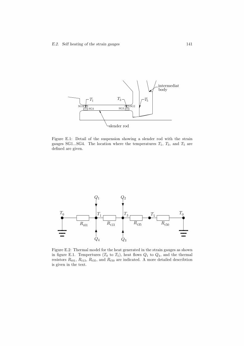
E.2. Self heating of the strain gauges 141
T T T1 3 5
SG1SG4 SG3
SG2
intermediatbody
slender rod
Figure E.1: Detail of the suspension showing a slender rod with the straingauges SG1...SG4. The location where the temperatures T1, T3, and T5 aredefined are given.
R R R Rt01 t13 t35 t50
Q Q
Q Q
1 2
4 3
T T T T T0 1 3 5 0
Figure E.2: Thermal model for the heat generated in the strain gauges as shownin figure E.1. Tempertures (T0 to T5), heat flows Q1 to Q4, and the thermalresistors Rt01, Rt13, Rt35, and Rt50 are indicated. A more detailed describtionis given in the text.

142 Appendix E. Error analysis of the probe system based on strain gauges
Figure E.3: Top view of the silicon dye with the suspension. The inner edgewhere the thickness of the silicon starts to increase is dashed.
rod. Symbols used in drawing E.2 are:
T0 temperature of the probe house and the surrounding airT1 temperature of the rod at a point between the first and the fourth
strain gaugeT3 temperature of the rod at a point between the second and the thirth
strain gaugeT5 temperature of the intermediate body
Q1..4 heat generated in every strain gaugeRt01 thermal resistance between the point marked T1 and the probe
houseRt13 thermal resistance between the points marked T1 and T3Rt35 thermal resistance between the points marked T3 and T5Rt50 thermal resistance between the point marked T5 and the surround-
ing air
Rt01, Rt13, and Rt35 are dominated by conduction and can be calculated by astandard equation giving the thermal resistance for a rectangular shaped pieceof material with dimensions l, w, t (length, width and thickness) and thermalconductivity λ:
Rt =l
λwt(E.2)
Rt01 is built up of two contributions: a length le = 0.15 mm from the middle ofstrain gauges one and four to the edge of the rod, and the part of the suspensionbridging the thick outer ring with the slender rods. The last part is differentfor each rod, but it is typically as wide as it is long, as can be seen in figureE.3. Rt01 can therefore be estimated as:
Rt01 =le
λSiwsts+
1
λSits=
0.15
0.15 · 0.16 · 0.02 +1
0.15 · 0.02 = 645 K W−1, (E.3)
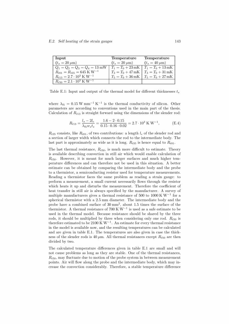
E.2. Self heating of the strain gauges 143
Input Temperature Temperature(ts = 20 µm) (ts = 20 µm) (ts = 40 µm)Q1 = Q2 = Q3 = Q4 = 13 mW T1 = T0 + 23mK T1 = T0 + 13mKRt01 = Rt35 = 645 K W−1 T3 = T0 + 47mK T3 = T0 + 31mKRt13 = 2.7 · 103 K W−1 T5 = T0 + 36mK T5 = T0 + 27mKRt50 = 2.1 · 103 K W−1
Table E.1: Input and output of the thermal model for different thicknesses ts
where λSi = 0.15 W mm−1 K−1 is the thermal conductivity of silicon. Otherparameters are according to conventions used in the main part of the thesis.Calculation of Rt13 is straight forward using the dimensions of the slender rod:
Rt13 =ls − 2leλSiwsts
=1.6− 2 · 0.15
0.15 · 0.16 · 0.02 = 2.7 · 103 K W−1, (E.4)
Rt35 consists, like Rt01, of two contributions: a length le of the slender rod anda section of larger width which connects the rod to the intermediate body. Thelast part is approximately as wide as it is long. Rt35 is hence equal to Rt01.
The last thermal resistance, Rt50, is much more difficult to estimate. Theoryis available describing convection in still air which would enable calculation ofRt50. However, it is meant for much larger surfaces and much higher tem-perature differences and can therefore not be used in this situation. A betterestimate can be obtained by comparing the intermediate body and the probeto a thermistor, a semiconducting resistor used for temperature measurements.Reading a thermistor faces the same problem as reading a strain gauge: toperform a measurement, a small current necessarily flows through the resistorwhich heats it up and disturbs the measurement. Therefore the coefficient ofheat transfer in still air is always specified by the manufacturer. A survey ofmultiple manufacturers gives a thermal resistance of 500 to 1000 K W−1 for aspherical thermistor with a 2.5 mm diameter. The intermediate body and theprobe have a combined surface of 30 mm2, about 1.5 times the surface of thethermistor. A thermal resistance of 700 K W−1 is used as a safe estimate to beused in the thermal model. Because resistance should be shared by the threerods, it should be multiplied by three when considering only one rod. Rt50 istherefore estimated to be 2100 K W−1. An estimate for every thermal resistancein the model is available now, and the resulting temperatures can be calculatedand are given in table E.1. The temperatures are also given in case the thick-ness of the slender rods is 40 µm. All thermal resistances except Rt50 are thendivided by two.
The calculated temperature differences given in table E.1 are small and willnot cause problems as long as they are stable. One of the thermal resistances,Rt50, may fluctuate due to motion of the probe system in between measurementpoints. Air will flow along the probe and the intermediate body, which may in-crease the convection considerably. Therefore, a stable temperature difference
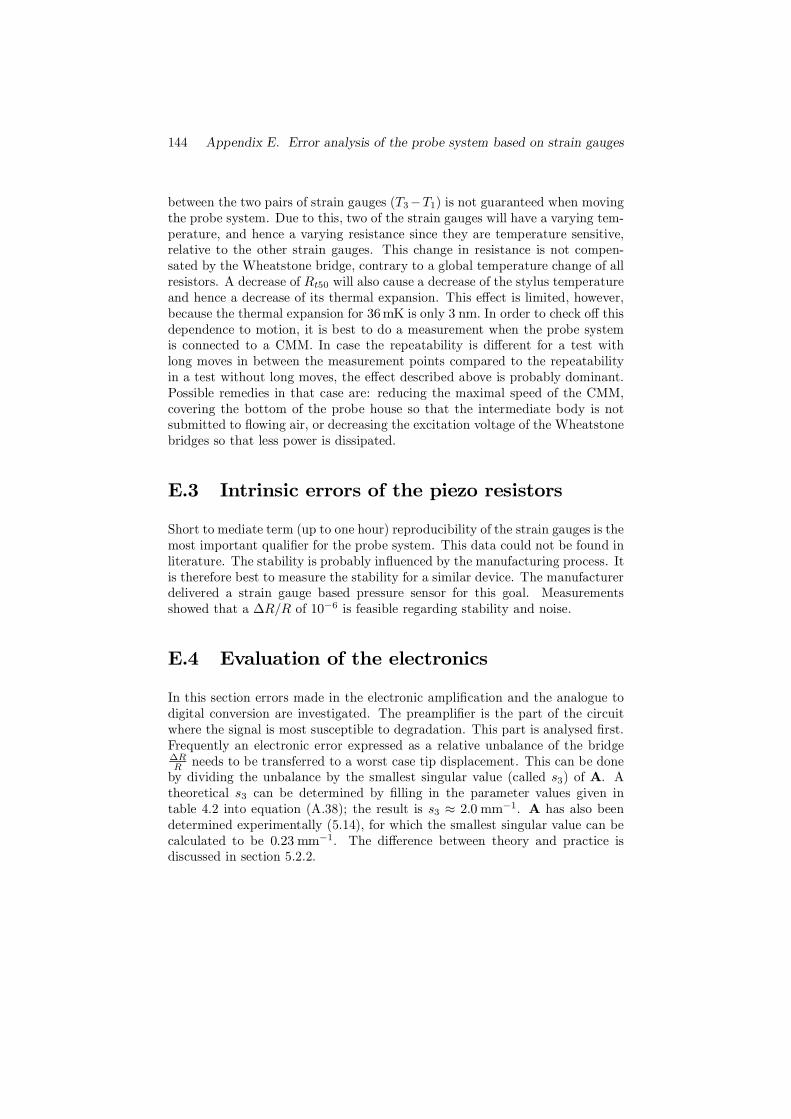
144 Appendix E. Error analysis of the probe system based on strain gauges
between the two pairs of strain gauges (T3−T1) is not guaranteed when movingthe probe system. Due to this, two of the strain gauges will have a varying tem-perature, and hence a varying resistance since they are temperature sensitive,relative to the other strain gauges. This change in resistance is not compen-sated by the Wheatstone bridge, contrary to a global temperature change of allresistors. A decrease of Rt50 will also cause a decrease of the stylus temperatureand hence a decrease of its thermal expansion. This effect is limited, however,because the thermal expansion for 36mK is only 3 nm. In order to check off thisdependence to motion, it is best to do a measurement when the probe systemis connected to a CMM. In case the repeatability is different for a test withlong moves in between the measurement points compared to the repeatabilityin a test without long moves, the effect described above is probably dominant.Possible remedies in that case are: reducing the maximal speed of the CMM,covering the bottom of the probe house so that the intermediate body is notsubmitted to flowing air, or decreasing the excitation voltage of the Wheatstonebridges so that less power is dissipated.
E.3 Intrinsic errors of the piezo resistors
Short to mediate term (up to one hour) reproducibility of the strain gauges is themost important qualifier for the probe system. This data could not be found inliterature. The stability is probably influenced by the manufacturing process. Itis therefore best to measure the stability for a similar device. The manufacturerdelivered a strain gauge based pressure sensor for this goal. Measurementsshowed that a ∆R/R of 10−6 is feasible regarding stability and noise.
E.4 Evaluation of the electronics
In this section errors made in the electronic amplification and the analogue todigital conversion are investigated. The preamplifier is the part of the circuitwhere the signal is most susceptible to degradation. This part is analysed first.Frequently an electronic error expressed as a relative unbalance of the bridge∆RRneeds to be transferred to a worst case tip displacement. This can be done
by dividing the unbalance by the smallest singular value (called s3) of A. Atheoretical s3 can be determined by filling in the parameter values given intable 4.2 into equation (A.38); the result is s3 ≈ 2.0 mm−1. A has also beendetermined experimentally (5.14), for which the smallest singular value can becalculated to be 0.23 mm−1. The difference between theory and practice isdiscussed in section 5.2.2.

E.4. Evaluation of the electronics 145
-
+
~
~R
R
C
½V
-½VV
INA118
i+
i-
1
m
mout
10 nF
Figure E.4: The equivalent circuit of the preamplifier part of the full circuitplotted in figure 4.2. The series resistors Ri− and Ri+ are both equal to half ofthe nominal strain gauge resistance (10 to 20 kΩ, depending on the prototype).
E.4.1 Errors in the preamplifier
As preamplifier, the INA118 made by Burr-Brown was selected, mainly becauseof its low noise and low power dissipation. Specifications can be found in thedata sheet supplied by the manufacturer [Burr-Brown INA118]. Possible errorsources in the preamplifier are (in order of importance):
• noise• drift of the zero point• non-linearity• drift of the gain• common mode leak through• power supply leak through
Noise
To estimate the signal degradation due to noise, the equivalent circuit, givenin figure E.4, is used. The noise arises from two effects at the inputs of theoperational amplifier: voltage noise over the inputs and current noise throughboth inputs. The current noise can only flow away via the two series resistorsRi− and Ri+, and will generate a voltage noise over these resistors. The totalnoise is the quadratic sum of the mentioned noise voltages. The OperationalAmplifier (OpAmp) noise voltage is specified as 25nV Hz−
1
2 at a frequencyof 1 Hz. This implies a 79nV Root Mean Square (RMS) voltage noise for a
bandwidth of 10 Hz. The current noise is specified as 6pA Hz−1
2 at a frequencyof 1 Hz, which causes a voltage noise of 190nV RMS over both series resistors.

146 Appendix E. Error analysis of the probe system based on strain gauges
The quadratic sum of these noise voltage at input of the OpAmp and over thetwo series resistors is:
Vn =√
792 + 2 · 1902 = 280nV (E.5)
For a 1 V Wheatstone bridge excitation voltage, Vn would be equivalent to arelative change of the piezo resistors of ∆R
R= 3 · 10−7. This corresponds to a
noise level of 0.15 nm or 1.3 nm for the theoretical or the experimental A-matrixrespectively. Both are well within the uncertainty requirement of 20 nm.
Drift of the zero value of the OpAmp
Drift in the zero value of the INA118 can be caused by a drift in the offsetvoltage19 or the bias current20 of the OpAmp. The temperature drift of theoffset voltage is specified as 700nV K−1. The maximum temperature variationof the probe system surroundings is specified as 0.1 K. The maximum offsetvoltage drift is therefore 70nV and can be neglected. The drift in the biascurrent is specified as 40pA K−1. The changing offset current difference causesa changing voltage difference over the two 10 kΩ series resistors. The maximumchange in the difference of the series resistor voltages is hence 40nV and can beneglected.
Non-linearity
The non-linearity of the INA118 is specified as 0.002% of the full scale range.The maximum output swing is 5 V. The non-linearity is hence 100 µV at theoutput, or 1 µV at the input. Since the working range of the sensors is only asmall part of the full range of the OpAmp, it is not likely that the full amount ofnon-linearity will show up in real measurements. This error source is thereforeneglected.
Drift of the gain
The drift of the gain is determined by the internal gain drift of the OpAmp(specified as 10ppm K−1) and the resistor that sets this gain, which has atemperature coefficient of 50ppm K−1. For a full scale range of 5 V at theoutput, this implies a maximum signal drift of 300 µV K−1, or 0.3 µV at theinput for a temperature variation of 0.1 K. If the OpAmp is operated near thecenter of its range, this error will be much smaller. In practice this is alwaysthe case, so also this error can be ignored.
19To reach an output voltage of zero volt, an ideal OpAmp would have equal input voltages.In practice zero output is reached with small difference between the inputs called offset voltage.See Horowitz and Hill [Horowitz 89] for more information.20 Ideally an OpAmp would have zero input current. In practice each input sinks or sources
a small current called offset current. The difference between the two offset currents is calledbias current. See Horowitz and Hill [Horowitz 89] for more information.
E.5. Summary 147
Common mode leak through
The common mode rejection ratio is specified as 107dB. This means that anequal change of both amplifier inputs (common mode) is amplified to the same
output as a input difference voltage of 10107
20 smaller size. A common modechange of 0.2 V would amplify as a 1 µV input difference signal. Commonmode variations of this size are not expected.
Power supply leak through
The power supply mode rejection ratio is specified to be better than 130dB forboth inputs and a gain of 100. This implies that the power supply would needto change by 3 V to cause a 1 µVmeasurement error. Since a separate stabilisedpower supply is used for the analogue part of the electronics (the digital parthas its own supply), such a large change will not occur.
E.4.2 Other electronic error sources
Two potential error sources not due to the preamplifier are investigated.
Reference voltage instability
A change of the reference voltage will change the excitation voltage of the bridgesand hence cause a proportional error of the bridge and preamplifier outputsignal. The ADC uses the same reference voltage to compare its inputs to. Anychange in the reference voltage is therefore automatically compensated by theADC and this error can be ignored.
ADC errors
Thanks to the preamplifier, the signal level at the ADC input is well abovecritical limits concerning noise and drift. Non-linearity is specified as 0.0015%,or 1 nm for a 65 µm range.
E.5 Summary
Summarising it can be stated that three error sources may have a significantcontribution: errors due to thermal expansion, and errors due to self heating.Thermal expansion is 450 nm K−1. Correction, either in hardware via a com-pensation somewhere else in the thermal loop of the CMM, or in software bymeasuring the temperature, is needed. Mechanical errors due to self heating

148 Appendix E. Error analysis of the probe system based on strain gauges
of the stylus are maximally 3 nm,but probably less. Due to self heating thetemperature of some of the strain gauges is about 20mK higher than the other.If this temperature varies it may influence the measurement. This is best testedin practice using a CMM. Errors caused by the electronics are all smaller than1 nm, hence they will have a limited contribution only.

Appendix F
Analyses of the A-matrix fit
procedure
It has been shown in chapter 5 that the sensitivities of the three horizontalcalibration moves should add to zero, which is not the case. Five possiblecauses where mentioned, which are repeated here:
1.−→Xt1 +
−→Xt2 +
−→Xt3 = 0 due to imperfections of the calibration setup. These
imperfections include:
(a) the orientation of the probe system relative to the calibration plat-form is not according to specification,
(b) the calibrator movement is not perpendicular to the platform,
(c) the probe shifts over the surface of the extender bar,
2. The A-matrix is not constant because it depends on:
(a) the probe orientation,
(b) the probing direction.
Of these possibilities, the most likely to occur is 1c: the probe shifts over thesurface. Why the other possibilities are less likely, is explained at the end ofthis appendix.
The probe tip shifts over the surface of the extender bar (1c) Itis implicitly assumed that the probe is not shifting over the surface of theextender bar. If it does, the actual displacement of the probe is different fromthe assumed direction which will disturb the calibration. When the probe iscalibrated over a larger distance than the up to now presented 4 µm, it can be
149

150 Appendix F. Analyses of the A-matrix fit procedure
seen that some calibration directions show a large hysteresis. The residuals (incalibrator coordinates) are plotted for tip motions in (0,0,−1), (−1, 0,0), and(− 1
2 ,12
√3,0) directions (figures F.1, F.2, and F.3 respectively). Due to breaking
of the first prototype, a different specimen of the probe system had to be used.However, it showed the same behaviour as presented in chapter 5. The plots
0 2 4 6 8 10-50
0
50
100
displacement in µm
resid
ual
in n
m
residuals for probing in (0,0,-1)-direction
z
y
x
Figure F.1: Residuals in x-, y-, and z-directions of the probe being moved in(0, 0,−1) direction (probe coordinates)
show that this hysteresis occurs almost entirely in x- or y-direction (in calibratorcoordinates), i.e. perpendicular to the calibration direction. This suggests thatthe probe is shifting over the surface. Shifting goes together with friction, andfriction causes hysteresis. There is no other plausible theory that can explainthis hysteresis and the absence of hysteresis in the calibration direction at thesame time.
This explanation raises new questions:
A Apparently there is a tendency to tip motion in a direction perpendicularto the calibration direction, so there must be a sidewards force. However,theory predicts that tip displacements in the direction of the stylus orperpendicular to it cause counter forces parallel to the displacement di-rection, i.e. theoretically there are no sidewards forces in the calibrationdirections used (see equation (A.11)).
B Hysteresis clearly shows up for large moves in the (1, 0, 0) direction, some-what less for large moves in other directions, and completely not for thesmaller (4 µm) moves. There should be sidewards motion for the smaller
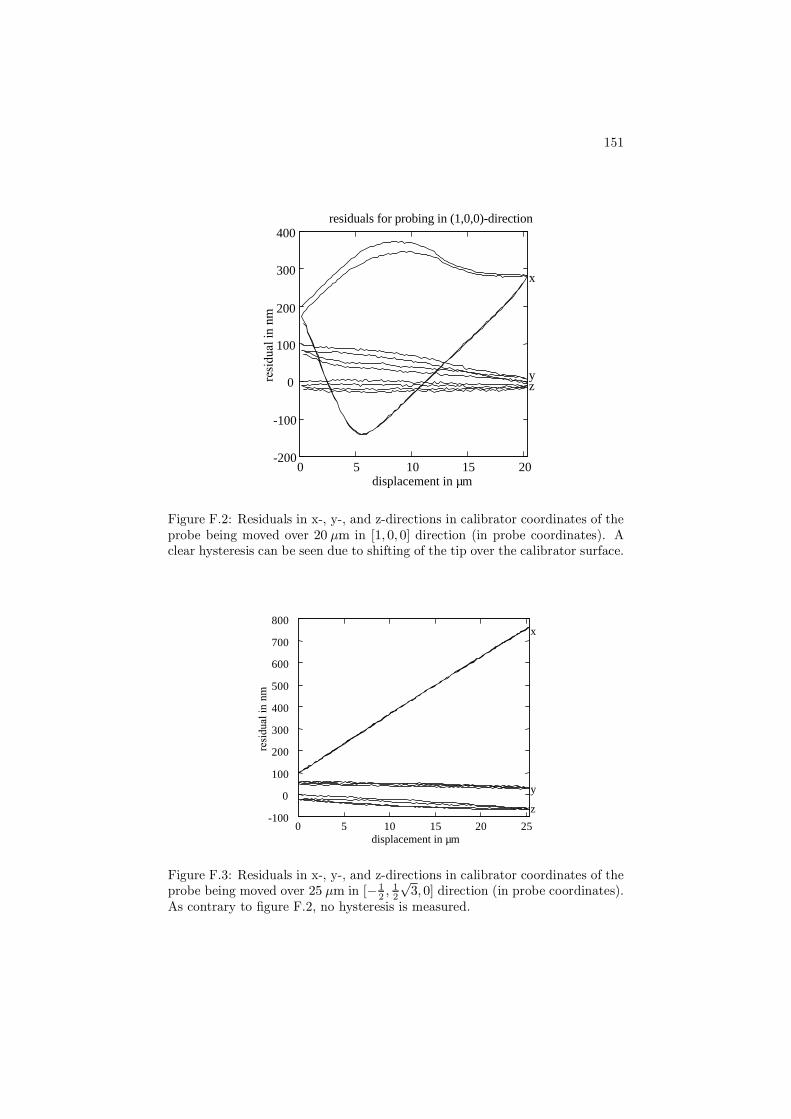
151
0 5 10 15 20-200
-100
0
100
200
300
400
displacement in µm
resi
dual
in
nm
residuals for probing in (1,0,0)-direction
zy
x
Figure F.2: Residuals in x-, y-, and z-directions in calibrator coordinates of theprobe being moved over 20 µm in [1,0,0] direction (in probe coordinates). Aclear hysteresis can be seen due to shifting of the tip over the calibrator surface.
0 5 10 15 20 25-100
0
100
200
300
400
500
600
700
800
displacement in µm
resid
ual
in n
m
z
y
x
Figure F.3: Residuals in x-, y-, and z-directions in calibrator coordinates of theprobe being moved over 25 µm in [− 1
2, 12
√3,0] direction (in probe coordinates).
As contrary to figure F.2, no hysteresis is measured.

152 Appendix F. Analyses of the A-matrix fit procedure
moves, otherwise the inconsistency present in equation (5.16) can stillnot be explained. Apparently there is sidewards motion without muchfriction.
The sidewards forces (question A) can be explained by the anisotropy of silicon,which effect has been neglected in the theory in appendix A, more specificequations (A.1) to (A.4). To model the anisotropy, the Young’s and shearmoduli in these equations should be replaced by fourth rank tensors. Adaptationof these equations will change the calculated stiffness of the probe system (A.11).It should not affect the theoretical A-matrix, since it could have been calculatedwithout the use of forces, only making use of the property that the elasticity isuniform over each slender rod. The strain gauges themselves are polycrystallineand hence have no direction dependence. The fact that the calculated A-matrixdoes not depend on material properties except for the gauge factor, is anotherindication thatA is not influenced by the anisotropy of silicon. The use of tensorcalculus can be prevented, because all stiffnesses in (A.1) to (A.4) depend on thecounter force in the length direction of the rod due to an elongation of the rod inits length direction. The only exception is rotation around its length axis, whichdepends on the shear modulus. It is sufficient if the Young’s modulus and theshear modulus in (A.1) to (A.4) are considered direction dependent. Wortmanand Evans described how to calculate the direction dependent Young’s modulusand shear modulus starting from the tensor elastic constants [Wortman 65].They also calculated the moduli for common directions. It appears that theYoung’s modulus for rods two and three are equal (1.57 · 1011 N m−2), butdifferent from rod 1 (1.30 ·1011 N m−2). The same applies to the shear modulus,0.55 ·1011 N m−2 for rod 2 and 3, and 0.8 ·1011 N m−2 for rod 1. To incorporatethis in the stiffness model, Es and Gs in equations (A.3) and (A.4), whichcalculate the stiffness matrices for rods two and three, are replaced by γEEs
and γGGs respectively. This leads to a stiffness matrix C describing the probingforces due to a tip translation as given in equation (F.1). Fx
FyFz
= C
TpxTpyTpz
C ≈
154 1 331 172 −233 −2 939
N m−1 (F.1)
Originally (see (A.11)), displacement in vertical or horizontal directions causedcounter forces parallel to the displacement direction. Equation (F.1) shows thatthis is no longer true if an anisotrope material like silicon is used for the slenderrods. Apart from parallel counter forces, there is also a force in x-direction for az-displacement and vice versa. Other off-diagonal elements of C are still small.
To understand what is going on intuitively, it is easiest to consider the extremecase where rod two and three can only rotate, but are not allowed to move inz-direction (in the probe system frame). For a tip translation in x-direction, the

153
axis of rotation goes necessarily through the end points of rods two and three.Consequently the stylus will move in z-direction. A z-translation of the tip willforce the intermediate body to rotate along the axis through the end pointsof rod two and three, which causes, apart from the z-translation, a motion inx-direction. Of course fixing rod two and three vertically is an extreme case,but making them stiffer compared to rod one, will cause the same kind of effectsalthough to a lesser extent.
uu
u
vv
v
M F
elasticstandstill mixed slidingsliding
Figure F.4: Basic mass spring model. The displacement of the free end of thespring is plotted agians the displacement of the mass, on the left side accordingto the Coulomb model, on the right side for a model that predics elastic motionfor small forces.
The second question posed above (B) can be explained because the Coulombfriction model breaks down for small displacements [Johnson 85]. Coulomb’smodel predicts that sliding only occurs when a certain force is exceeded. Atsmaller forces the body remains at standstill. This is explained in figure F.4where a body M is pulled over a surface via a spring C. Suppose the free end ofthe spring makes a back and forth movement. The position of the body M (v)is plotted against the position of the free end of the spring (u) at the left sideof figure F.4. For small u the body will not move. At a certain u, M will startmoving and recovers part of the distance u has already travelled. Finally u andv increase at the same pace: the line makes a 45 angle with u-axis. For smallmotions, however, Coulomb’s model should be replaced by a three regime model:for small u and v the behaviour is elastic. For large u, sliding will occur like inCoulomb’s model, with ∆u = ∆v. For moderate u, the motion will be partlyelastic and partly due to sliding. v is plotted against u again for a back andforth movement of u (right side plot of figure F.4). The probe tip sliding over asurface can be translated to the body-spring system by considering v to be the

154 Appendix F. Analyses of the A-matrix fit procedure
sidewards motion of the tip, and u to be that displacement of the tip that wouldcancel the sidewards force. Hysteresis will only occur when the probe slides overthe surface. For small calibration movements, the sidewards translations willremain in the elastic regime, and no hysteresis will occur. For larger motions, thesidewards translation will enter the mixed regime. This will occur in the (1, 0, 0)direction first, because the sidewards force is twice as large compared to the(− 1
2 ,12
√3,0)and
(− 12 ,− 1
2
√3, 0)directions, since the x-displacement is twice as
large. This is in agreement with the measurements, where the (1,0,0) directionshows clearly more hysteresis than the
(− 12 ,± 1
2
√3,0)directions (figure F.2 and
F.3).
The residual curve of the probe shifting over the surface should look like theone given at the right hand side of figure F.4, only u is now replaced by thetravelled distance in the calibration direction. Since this distance has a linearrelationship with u, the scaling will be different. A nice example is shown infigure F.5, where the residuals in the calibrator coordinate frame are plotted.
0 0.5 1 1.5 2 2.5 3 3.5 40
200
400
600
800
1000
1200
1400
displacement in µm
resid
ual
in n
m
z
y
x
residuals when probing under large angle
Figure F.5: Residuals in x-, y-, and z-directions, expressed in calibrator coordi-nates, of the probe being moved in (− sin55 ,0,− cos 55 ) = (−0.82,0,−0.57)direction (in probe coordinates). Note the large hysterysis due to slip over thecalibrator surface.
The stylus makes an angle of 55 with the z-axis, and the probe is moved in(− sin55 ,0,− cos 55 ) = (−0.82, 0,−0.57) direction (probe coordinates). Ifwe look back to the calibration in (1,0,0) direction, it can be seen that thehysteresis curve looks different (figure F.2). In particular, the curve starts
155
steep and flattens at the end, which is inconsistent with the described slidingmodel. Probably this is due to a faulty calibration of the A-matrix. In order tocalculate A, it was assumed that the probe would not move perpendicular tothe calibration direction. As discussed, this assumption was probably invalid. Asmall modification in A can flip the x-residual to the other side of the horizontalaxis, in which case a looks much more like typical hysteresis.
Conclusively it can be stated that the small scale elastic friction effect canexplain why hysteresis shows up only for larger distance moves in some directionsand never for small distance moves. In the remainder of this appendix it isexplained why the other explanations stated at the beginning of this appendixare less likely to occur.
The orientation of the probe system relative to the calibration plat-form is not according to specification (1a). It has been verified by aCMM measurement that the probe system adapter ((15) in figure 5.10) is ori-ented relative to the calibrator platform according to specification. It couldnot be verified how the suspension itself is oriented in the probe system andhow the probe system is oriented in the adapter. However, a misorientation ofthe suspension or the probe system can not explain the experimental inconsis-tency discussed here. SupposeA is the transformation matrix for untilted probesystem. Any rotation of the probe system can be transferred to the unrotatedsystem by a rotation matrix R. Hence a matrix A′ =AR can be defined. SinceR is fixed to the probe system and expressed in probe system coordinates, itdoes not change when another position in the nine position stand is chosen.So, due to a misorientation of the probe system or the suspension, a differentA would be found, but it would still be valid for all orientations of the probesystem. It can therefore be concluded that a misorientation of the probe systemcan not be the cause of inconsistency under discussion.
The calibrator movement is not perpendicular to the platform (1b)A sideways displacement during the vertical travel of the measurement mirrorcauses faulty calibration of the probe system. Because the probe system isoriented in different directions depending on how the probe system is connectedto the nine position stand, the translation will have a different direction foreach calibration run, when expressed in the probe system coordinate frame.The parasitic displacement of the measurement mirror has been measured in atwo step measurement.
It has been verified, using a CMM, that the top side of the measurement mirroris parallel to the platform. Parasitic translation could not be measured withsufficient accuracy by that CMM, due to the travel of the measurement mirrorof 30 µm only. An angular uncertainty of 25 mrad (being the angle that wouldexplain the experimental inconsistency) would require a 0.1 µm uncertainty ofthe CMM, ten times less than what is available. A Fizeau interferometer isused instead. This interferometer can measure the displacement of a plane in

156 Appendix F. Analyses of the A-matrix fit procedure
the direction normal to the plane. A gauge block is placed on the top side ofthe measurement mirror. One of the side planes of the gauge block is used asplane for the Fizeau interferometer. The orthogonality of this mirror to theplatform of the calibrator is secured by the given orthogonality of the gaugeblock and the measured parallelism of the measurement mirror with respectto the platform. The outcome of this measurement is that the rotation of theaxis of motion and the platform normal is smaller than 4 mrad. This can onlyexplain a small fraction (15%) of the abnormality seen in figure 5.18 to 5.21.
The A-matrix depends on the orientation of the probe system (2a)One of the prerequisites of the calibration procedure to be valid is that theA-matrix should not depend on the orientation of the probe system. If A doesdepend on the probe system orientation, the calibration is invalid. This would,for example, be the case if the A-matrix changes when the probe system isrotated from a vertically oriented stylus to a horizontally oriented stylus. Thisis only possible if some kind of field is interacting with the probe system. Thefield could be for example gravity or an electric or magnetic field. Since onlythe sensitivities of the Wheatstone bridges to probe displacements are used tocalculate A, the field should have an influence on the sensitivity in order toexplain the inconsistency. A field that only causes an offset in the measuredprobe position, can not be the explanation, unless the offset is so large thatnon-linearities in transformation of the Wheatstone bridges readings to probedisplacement become important.
Gravity, for example, will cause an offset but has no obvious effect on thesensitivity. The sagging due to gravity is about 2 µm in both horizontal asvertical direction. Since no substantial non-linearity is measured in the 4 µmcalibration curves, the 2 µm offset can not explain why it is not possible to fita single A-matrix to the data.
It has been detected that light has an influence on Wheatstone bridge read outs.However, the experiments are performed in darkness. Even if some light wouldseep through the holes in the isolating box (it has some holes to give entranceto interferometer light beams and cables), it would cause an offset. Sound andvibrations can only cause dynamic effects. It is not likely that at the position ofthe strain gauges there are magnetic or electrical fields present strong enoughto influence the measurement.
To sum up it may be stated that there is no clear reason why the sensitivity ofthe probe system would depend on its orientation. On the other hand, insen-sitivity can not be guaranteed and a true 3D calibration in a fixed orientationis preferred. This setup would most likely be a high accurate, small volumeCMM.
A single A-matrix does not exist (2b) It could be that there is simply nosingle A-matrix valid for all probing directions. If the A-matrix would depend

157
on the direction of the probe system, the calibration procedure that is followedis invalid. A direction dependent A-matrix, however, would be contradictoryto the theory described in appendix A, and, more specific, equation (A.37) and(A.38). That could be the case if one of the approximations is invalid. However,most approximations are first order approximations leading to non straight lineresponse of the Wheatstone bridge measurements. The effect showing up in themeasurements, straight line response in an unexpected direction, can not beexplained by invalid first order approximations.
Suppose, notwithstanding the theoretical problems, that the sensitivity of thebridges would be different for positive directions compared to negative direc-tions. That could explain the fit problem. However, the zero point of themeasurements is not one to one related to the natural zero point were the strainis zero. The relation between the two will depend on the sagging of the probeand the internal stresses in the slender rods. The two zero points coincidingwould be highly accidental. If they do not coincide, then a knee would be visiblein the measurements, which is not the case. It can therefore be stated that adirection dependent A-matrix is unlikely.


Bibliography
[Ashcroft 76] N.W. Ashcroft, N.D. Mermin, Solid State Physics,ISBN0-03-049346-3, Saunders College Philadelphia,1976.
[Binas 86] G. Verkerk, J.B. Broens, W. Kranendonk, F.J. v.d.Puijl, J.L. Sikkema, C.W. Stam, Binas, Informatieboekvwo/havo voor het onderwijs in de natuurwetenschap-pen (in dutch), ISBN 90 01 89351 1, Wolters-NoordhoffGroningen, 1986.
[Bouwhuis 85] G. Bouwhuis, J. Braat, A. Huijser, J. Pasman, G. vanRosmalen K. Schouhamer Immink, Principles of OpticalDisc Systems, ISBN 0-85274-785-3, AdamHilger LTD,Bristol and Boston, 1985.
[Brouwer 64] W. Brouwer, Matrix methods in optical instrument de-sign, W.A. Benjamin Inc, New York and Amsterdam,1964.
[Burr-Brown INA118] Data sheet of the INA118 operational amplifier manu-factured by Burr-Brown, downloadable from www.burr-brown.com.
[Claesen 92] E.T. Claesen, Het meetsysteem van de A.F.M. (indutch), MSc. thesis, Eindhoven University of Technol-ogy, 1992.
[Cosijns 02] S.J.A.G. Cosijns, H. Haitjema, P.H.J. Schellekens, Mod-eling and verifying non-linearities in heterodyne displace-ment interferometry, Precision Engineering, 26(4), 412-424, 2002.
[Cuijpers 95] M.A.W. Cuijpers, Herontwerp van een refractometer (indutch), MSc. thesis, Eindhoven University of Technology,1995.
159
160 Bibliography
[Dubbel 81] W. Beitz, K.H. Küttner, Taschenbuch für den Maschi-nenbau, ISBN 3-540-67777-1, Springer-Verlag Berlin,1981.
[Elwenspoek 96] M. Elwenspoek e.a.; Micromechanics, Etching of silicon;lecture notes of the Twente University, 1996.
[Florussen 02] G.H.J. Florussen, Accuracy Analysis of Multi-axis Ma-chines by 3D Length Measurements, PhD thesis, ISBN90-386-2943-5, Eindhoven University of Technology,2002.
[GUM 95] Guide to the expression of Uncertainties in Measure-ment, ISBN 92 67 101889, ISO-1995, Switzerland, 1995.
[Haitjema 98] H. Haitjema, N. Rosielle, G.Kotte, H. Steijaert, Designand calibration of a parallel-moving displacement genera-tor for nano-metrology, Meas. Sci. Technol. 9, 1098-1104,1998.
[Haitjema 00] H. Haitjema, P.H.J. Schellekens, S.F.C.L. Wetzels, Cal-ibration of displacement sensors up to 300 µm withnanometre accuracy and direct traceability to a primarystandard of length, Metrologia, 37(1), 25-34, 2000.
[Haitjema 01] H. Haitjema, W.O. Pril, P.H.J. Schellekens, Developmentof a silicon-based nanoprobe system for 3-D measure-ments, Annals of CIRP, 50(1), 365-368, 2001.
[Haitjema 01a] H. Haitjema, W.O. Pril, P.H.J. Schellekens, Asilicon-etched probe for 3-D coordinate measurementswith an uncertainty below 0,1 micrometer, IEEETrans.Inst.Meas., 50(6), 1519-1523, 2001.
[Hecht 90] E. Hecht, Optics, ISBN 0 201 11609 X, Addinson-Wesleypublishing company, 1990.
[Hidaka 99] K.Hidaka, N.Ishikawa, K.Nishimura, High accurace &high-response touch trigger probe for coordinate measur-ing machine, Euspen conference proceedings, 2, page 303- 306, 1999.
[Hocken 01] R.J. Hocken, D.L.Trumper, C.Wang, Dynamics and con-trol of the UNCC/MIT sub-atomic measuring machine,Annals of CIRP, 50(1), 373-376, 2001.
[Horowitz 89] P. Horowitz, W. Hill, The art of electronics, ISBN 0-521-37095-7, Cambridge University Press, Cambridge, 1989.
[Johnson 85] K.L. Johnson, Contact mechanics, ISBN 0-521-34796-3,Cambridge University Press, 1985.

Bibliography 161
[Kramar 98] J.A. Kramar, J. Jun, W.B. Penzes, F.E. Scire, E.C.Teague, J.S. Villarrubia, Grating pitch measurementswith the molecular measuring machine, Proc. SPIE,3806, 46-53, 1999.
[Levoisier 97] L. Levoisier, private communication, 1997.
[Lu 99] R. Lu, Design of a nanometer capacative probe, thesisfor Mechatronic Design post graduate course, ISBN 90-5282-936-5, Eindhoven University of Technology, 1999.
[Middelhoek 89] S. Middelhoek, S.A. Audet, Silicon Sensors, ISBN 0-12-495051-5, Academic Press, London 1989.
[Peggs 99] G.N. Peggs, A.J. Lewis, S. Oldfield, Design for a compacthigh-accuracy CMM, Annals of CIRP, 48(1), 417-420,1999.
[Petersen 82] K.E. Petersen, Silicon as a mechanical material, Pro-ceedings of the IEEE, 70(5), 420-457, 1982.
[Pril 97] W.O. Pril, K.G. Struik, P.H.J. Schellekens, Developmentof a 2D probing system with nanometer resolution, Pro-ceedings of the American Society of Precision Engineer-ing 1997 Annual Meeting, 438-442, 1997.
[Pril 95] W.O. Pril, Ontwikkeling van een 3D-CMM-tastsysteemmet nanometernauwkeurigheid (in dutch), thesis forMechatronic Design post graduate course, ISBN 90-5282-479-7, Eindhoven University of Technology, 1995.
[Przemieniecki 68] J.S. Przemieniecki, Theory of matrix structural analysis,McGraw-Hill, 1968.
[Ray-Choudhury 97] P. Ray-Choudhury, Handbook of Microlithography, Mi-cromachining and Microfabrication part 1 & 2, ISBN 0-8194-2378-5 & ISBN 0-85296-911-2 , SPIE Optical En-gineering Press, Bellingham, Washington USA, 1997.
[Ruijl 01] T.A.M. Ruijl, Ultra Precision Coordinate Measuring Ma-chine, PhD thesis, ISBN 90-6464-287-7, Delft Universityof Technology, 2001.
[Sartori 95] S. Sartori, G.X. Zhang, Geometric error measurementand compensation of machines, Annals of CIRP, 44(2),599-609, 1995.
[Schellekens 98] P. Schellekens, N.Rosielle, H. Vermeulen, M. Vermeulen,S. Wetzels, W. Pril, Design for precision: Current statusand trends, Annals of CIRP, 44(2), 557-586, 1998.

162 Bibliography
[Schoot 98] H. v.d. Schoot, private communication, 1998.
[Schouten 97] C.H. Schouten, P.C.J.N. Rosielle, P.H.J. Schellekens, De-sign of a kinematic coupling for precion applications,Precision Engineering, 20(1), 46-52, 1997.
[Schwenke 01] H. Schwenke, F. Wäldele, C. Weiskirch, H. Kunzmann,Opto-tactile sensor for 2D and 3D measurement of smallstructures on coordinate measuring machines, Annals ofCIRP, 50(1), 361-365, 2001.
[Sharp 88] Technical literature for laser diode model no.LTOH1OM, Sharp corporation electronic componentsgroup, 1988.
[Soons 93] J.A.S. Soons, Accuracy Analysis of Multi-Axis Machines,PhD thesis, Eindhoven University of Technology, 1993.
[Spaan 95] H.A.M. Spaan, Software error compensation of machinetools, PhD thesis, Eindhoven University of Technology,1995.
[Szabo 77] István Szabó, Höhere Technische Mechanic, Springer-Verlag Berlin Heidelberg New York, 1977.
[Takaya 99] Y. Takaya, S. Takahashi, T.Miyoshi, K.Saito, Develop-ment of the Nano-CMM Probe based on laser trappingtechnology, Annals of CIRP, 48(1), 421-424 1999.
[Taniguchi 83] N. Taniguchi, Current status in and future trends ofultra-precision machining and ultra fine materials pro-cessing, Annals of CIRP, 32(2), 573-582, 1993.
[TI TLC1078C] Data sheet of the INA118 operational amplifier man-ufactured by Texas Instruments, downloadable fromwww.ti.com.
[Vermeulen 95] M. Vermeulen, private communication, 1995.
[Vermeulen 98] M.M.P.A. Vermeulen, P.C.J.N. Rosielle, P.H.J.Schellekens, Design of a high-precision 3D-coordinatemeasuring machine, Annals of CIRP, 47(1), 447-451,1998.
[Vermeulen 99] M.M.P.A. Vermeulen, High Precision 3D-CoordinateMeasuring Machine: Design and Prototype-Development, ISBN 90-386-2631-2, PhD thesis,Eindhoven University of Technology.

Bibliography 163
[VIM 93] International Vocabulary of Basic and General Terms inMetrology (Vocabulaire International des Termes Fonda-mentaux et Généraux de Métrologie), ISBN 92-67-01075-1, International Organization for Standardization, 1993.
[Visscher 92] M. Visscher, The measurement of the filmthickness andthe roughness deformation of lubricate elastomers, PhDthesis, Eindhoven University of Technology, 1992.
[Visscher 94] M. Visscher and K.G. Struik, Optical profilometry andits application to mechaniclly inaccessible surfaces PartI: Principles of focus error detection, Precision Engineer-ing, 16(3), 192-198, 1994.
[Vliet 96] W. van Vliet, Development of a Fast Mechanical Probefor Coordinate Measuring Machines, ISBN 90-386-0168-9, PhD thesis, Eindhoven University of Technology, 1996.
[Wetzels 98] S.F.C.L. Wetzels, Laser Based Displacement Calibrationwith Nanometre Accuracy, ISBN 90-386-0730-X, PhDthesis, Eindhoven University of Technology, 1998.
[Wortman 65] J.J. Wortman, R.A. Evans, Young’s modulus, Shearmodulus and Poisson’s ratio in silicon and germanium,Journal of Applied Physics 36(1), 153-156, 1965.
[Young 89] W. C. Young, Roark’s Formulas for Stress & Strains,ISBN 0-07-100373-8, McGraw-Hill, 1989.
[Zhu 92] F. Zhu, Development of capacitive position transducersthrough a mechatronic approach, PhD thesis, ISBN 90-9005114-7, Delft university of Technology, 1992.


Acknowledgements
I well remember the day I visited the “open dag” of the TU/e post gradu-ate courses (SAI). At that day, Professor Schellekens convinced me that doingmechatronics with a physics background is both possible and fun. This way helaid the very basis for this thesis. During the research he stimulated me withhis never lasting optimism and enthusiasm. For all this I am much indepted tohim.
Furthermore, I am much obliged to the members of the core promotion com-mittee prof. dr. ing. L.M.F. Kaufmann, dr. H. Haitjema, prof. dr. ir. A.J.A.Vandenput, and prof. dr. ir. M.J.W. Schouten for the time they spent reviewingand improving this thesis.
The research described in this thesis has been performed at the Precision En-gineering group of the Eindhoven University of Technology. This project wasfinancially supported by Mitutoyo Corporation, STW and NMi and I would liketo thank these institutions.
I also would like to thank my fellow Ph.D.-students for their support and com-pany through the years. I benefitted greatly from the discussions with SergeWetzels. Yujian Fan supplied me with a lot of Chinese culture, including cook-ing. Guido Florussen was of great help, especially during the last stage of myPh.D. In addition I wish to express thanks to present and former staff members,Ph.D.-students and students of the section Precision Engineering who made mehave a pleasant time doing my PhD research.
A lot of people helped in realising the prototypes and I want to thank them fortheir efforts. The support from the university’s technical workshop (GTD) wasof priceless value. In specific I want to mention Lucien Cleven, Ruud van deBogaert, and the employees of Twente Micro Products (TMP).
Finally, a special word of thanks goes to my family, friends, and especially tomy wife Anke for their support, patience and encouragement.
165

Curriculum Vitae
Wouter Pril was born on May 13th, 1969 in Eindhoven, The Netherlands. Heattended the St. Willibrord Gymnasium, where he obtained his Gymnasiumdiploma in 1987. The same year, he started his physics study at the NijmegenUniversity. In March 1993 he received his Masters degree.
Immediately after his graduation, he started the post graduate coarse ‘Mecha-tronic Designer’ at the Stan Ackermans Institute of the Eindhoven Universityof Technology, for which he graduated in May 1995 as Master of TechnologicalDesign. The research described in this thesis is a continuation of the practicalwork done in the framework of the ‘Mechatronic Designer’ coarse. Since Octo-ber 1999 he works within the department ‘Mechatronic System Development’of ASML in Veldhoven.
166