Embed Size (px)
Citation preview
ABSTRACT
Title of Thesis: DEVELOPMENT OF A DEEP SILICON PHASE FRESNEL LENS USING GRAY-SCALE LITHOGRAPHY AND DEEP REACTIVE ION ETCHING Degree candidate: Brian C. Morgan Degree and year: Master of Science, 2004 Thesis directed by: Professor Reza Ghodssi Department of Electrical and Computer Engineering
A phase Fresnel lens (PFL) could achieve higher sensitivity and angular
resolution in astronomical observations than the current generation of gamma and hard
x-ray instruments. For ground tests of a PFL system, silicon lenses must be fabricated
on the micro-scale with controlled profiles to enable high lens efficiency. Thus, two
MEMS-based technologies, gray-scale lithography and deep reactive ion etching
(DRIE), are extended to create multiple controlled step heights in silicon on the
necessary scale.
A Gaussian approximation is introduced as a method of predicting a
photoresist gray level height given the amount of transmitted light through a gray-
scale optical mask. Etch selectivity during DRIE is then accurately controlled by
introducing an oxygen-only step to a standard Bosch cycle to produce the desired
scaling factor between the photoresist and silicon profiles. Finally, a profile
evaluation method is developed to calculate the expected efficiency of measured
silicon profiles. Calculated efficiencies above 87% have been achieved.
DEVELOPMENT OF A DEEP SILICON PHASE FRESNEL LENS
USING GRAY-SCALE LITHOGRAPHY AND DEEP REACTIVE ION ETCHING
By
Brian C. Morgan
Thesis submitted to the Faculty of the Graduate School of the University of Maryland, College Park in partial fulfillment
of the requirements for the degree of Master of Science
2004
Advisory Committee: Professor Reza Ghodssi, Chair Professor Christopher Davis Professor Thomas Murphy

©Copyright by
Brian C. Morgan
2004
ii
TABLE OF CONTENTS List of Tables……………………………………………………………………………. List of Figures…………………………………………………………………………… 1 Introduction
1.1 Astronomical Imaging Systems………………………..………………….……… 1.2 Fresnel Lenses………………………………………………………….………….
1.2.1 Fresnel Lens Derivatives…………………………………….…………….. 1.2.2 The proposed Fresnel Lens-based Telescope………………..……………...
1.3 Test Lens Considerations…………………………………………………..…….… 1.3.1 Material Selection……………………………………………………..…… 1.3.2 Dimensions…………………………………………………………………..
1.4 Micro-Electro-Mechanical Systems (MEMS) Fabrication………………………..... 1.4.1 Planar Fabrication………………………………………………………..….
1.4.1.1 Photolithography……………………………………………………….. 1.4.1.2 Surface Micromachining………………………………………………. 1.4.1.3 Bulk Micromachining………………………………………………….. 1.4.1.4 Planar micro-scale Fresnel Lenses……………………………………..
1.4.2 3-Dimensional MEMS Fabrication………………………………………… 2 Gray-scale Technology
2.1 Introduction……………………………………………………………………….. 2.2 Gray-scale Lithography……………………………………………………………
2.2.1 Gray-scale Mask Design…………………………………………………… 2.2.2 Lithography Processing…………………………………………………….
2.2.2.1 Photoresist Selection……………………………………………………. 2.2.2.2 Exposure………………………………………………………………… 2.2.2.3 Development…………………………………………………………….
2.2.3 Calibration Mask…………………………………………………………… 2.2.4 Standardized Lithography Process………………………………………….
2.3 Dry-anisotropic Etching……………………………………………………………. 2.3.1 Deep Reactive Ion Etching…………………………………………………. 2.3.2 Gray-scale Pattern Transfer………………………………………………… 2.3.3 Selectivity Control Experiments…………………………………………….
2.4 Summary……………………………………………………………………………
iv
v
12346689
101013141719
2223242627282931333434353741

iii
3 Optical Mask Design
3.1 Introduction……………………………………………………………………… 3.2 PFL Equations…………………………………………………………………..… 3.3 PFL Mask Design considerations…………………………………………….…..
3.3.1 Pitch Selection……………………………………………………….…… 3.3.2 Pixel Constraints……………………………………………………..…… 3.3.3 Choice of Gray Levels…………………………………………………… 3.3.4 Multiple Phase Depths……………………………………………………
3.4 Gaussian Approximation Method…………………………………………..……. 3.4.1 Experiment…………………………………………………………..……… 3.4.2 Integration into C Program Design………………………………..………
3.5 PFL Device Design Parameters…………………………………………..……… 3.6 Summary…………………………………………………………………………
4 PFL Fabrication and Evaluation
4.1 Introduction……………………………………………………………………… 4.2 Lithography Results………………………………………………………………
4.2.1 Photoresist PFL Structures……………………………………………….. 4.2.2 PFL Metrology (Photoresist)……………………………………………. 4.2.3 Gaussian Approximation Confirmation…………………………………..
4.3 Dry Etching Results……………………………………………………………... 4.3.1 General DRIE Results……………………………………………………. 4.3.2 DRIE with Oxygen-only Step……………………………………………. 4.3.3 Aspect Ratio Dependent Etching…………………………………………
4.4 Profile Evaluation……………………………………………………………….. 4.4.1 Method…………………………………………………………………… 4.4.2 Profile Measurements………………………………………………….… 4.4.3 Lens Design Comparison…………………………………………………
4.5 Summary………………………………………………………………………… 5 Summary and Future Work
5.1 Summary………………………………………………………………………… 5.2 Future Work………………………………………………………………………
5.2.1 ARDE Compensation…………………………………………………….. 5.2.2 Bulk Silicon Removal…………………………………………………….
5.3 Conclusion………………………………………………………………………. Bibliography………………………………………………………………………….
424245464850525354575960
6263636871727374808485889396
98101102103105
106
iv
LIST OF TABLES
Table 1.1: Three example PFL telescopes proposed by Skinner……………………. Table 2.1: List of gray-scale wedge structures designed on the calibration
mask…………………………………………………………………..…. Table 2.2: The standard gray-scale lithography process……………………….…….. Table 2.3: DRIE process parameters for Base Etch I……………………………...… Table 2.4: DRIE selectivity characterization results………………………………… Table 3.1: Mock selection of pixels using a 2.2 pitch and fictional design
rules……………………………………………………………………… Table 3.2: Gray level height data taken from a structures using a 2.8µm pitch……… Table 3.3: Properties of the 3 primary PFL’s designed for this research……………. Table 4.1: Modified Bosch process using an Oxygen-only step………………………. Table 4.2: Modulating the length of the O2 etch step and the resulting etch
selectivity………………………………………………………………… Table 4.3: Theoretical versus calculated lens efficiencies for various lens
profiles……………………………………………………………………. Table 4.4: Calculated efficiencies of a PFL with each radial scan taken at a
different angle from the horizontal…………………………………….… Table 4.5: Calculated efficiencies of PFLs at different locations across a
75mm wafer…………………………………………………………….…
5
33
33
37
39
50
54
60
75
77
87
89
92
v
LIST OF FIGURES
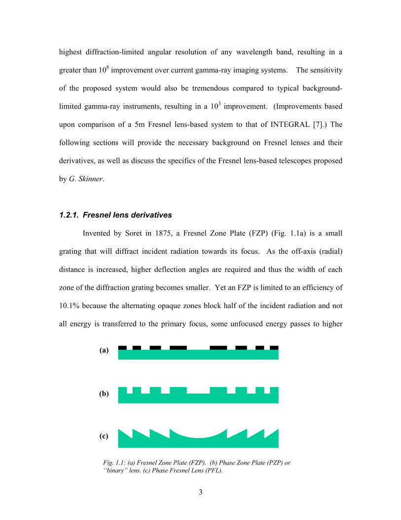
Figure 1.1: (a) Fresnel Zone Plate (FZP). (b) Phase Zone Plate (PZP) or “binary” lens. (c) Phase Fresnel Lens (PFL)………….……………....….
Figure 1.2: The thickness of different lens materials required to produce a π
phase shift [16]……..…….……….……….……….……….……….…. Figure 1.3: The amount of photon absorption through a material with a phase
shift of π [16].……….……….……….……….………….………….…. Figure 1.4: Photoresist patterns resulting from contact lithography using
positive or negative resist with the same optical mask………………….... Figure 1.5: A projection lithography system with reduction optics (usually 5X
or 10X).……….……….……….……….……….……….…...………… Figure 1.6: Surface micromachining to release a beam. (a) Sacrificial layer is
deposited and patterned. (b) Structural layer is deposited and patterned. (c) Sacrificial layer is selectively etched away leaving a free-standing beam.……….……….……….……….………..…………..
Figure 1.7: Illustration of wet isotropic etching with a small amount of mask
undercut.……….……….……….……….……….……….………….…. Figure 1.8: Illustration of wet anisotropic etching, where a 54.7% angle is
revealed between the (111) and the (100) planes in crystalline silicon.……….……….……….……….……….………….………….….
Figure 1.9: Plasma etching mechanisms: (a) Physical sputtering. (b) Chemical
etching. (c) Ion-assisted etching..……….……….……….…….………... Figure 2.1: Photoresist gray levels after development, on a silicon substrate………. Figure 2.2: Optical mask design scheme using sub-resolution pixels and a
constant sub-resolution pitch. By calculating the area of each pixel and the area of the pitch, the percent transmission through the mask is estimated.……….……….……….……….……….…………….
Figure 2.3: A photoresist gray-scale wedge structure after (a) over-
development, (b) under-development, and (c) appropriate development.….……….……….……….……….………….………….
3
7
7
12
12
13
14
15
16
22
25
30
vi
Figure 2.4: SEM images showing two gray levels produced using two different pitches on the gray-scale mask; (a) shows a pitch slightly above resolution and (b) shows a smoother photoresist surface using a pitch right at the resolution limit.……….……….……….……………...
Figure 2.5: The steps of deep reactive ion etching (DRIE). (a) Silicon wafer is
patterned with a masking material. (b) Etching step of the cycle etches the silicon similar to RIE. (c) Conformal passivation layer is deposited over entire wafer. (d) Etch step is repeated. Ion bombardment removes the passivation layer from horizontal surfaces, while sidewalls remain protected. (e) Passivation step is repeated to cover the newly exposed sidewall. (f) Etch step repeats. (g) Vertical trench achieved with slight sidewall scalloping.……………..
Figure 2.6: (a) Initial sloped photoresist structure on silicon. (b) Sloped
pattern begins to transfer into the silicon with a certain selectivity. (c) Final structure in silicon retains lateral dimensions while vertical dimensions are amplified by the etch selectivity.………………….
Figure 2.7: SEM showing the structures used to measure the inside sidewall
angle and outside sidewall angle.……….……….……….……….……. Figure 3.1: Example PFL profile with a focal length of 118m for 8.4keV
photons…………….……….……….……….……….……….……….. Figure 3.2: The 4π phase depth shifts every other grating vertically. This
effectively doubles the width of each grating.……….…………………. Figure 3.3: An example pixel layout near the boundary of one ridge……….……… Figure 3.4: Rectangular pixilation schematic used to define mask design
constraints.……….……….…………….……….……….…………….. Figure 3.5: Gaussian curve fit through data points relating normalized
photoresist heights to the percent transmission through the mask that caused them.……….……….……….……….……….………….….
Figure 4.1: The first demonstration of a photoresist PFL.……….………………..… Figure 4.2: PFL ridge exhibiting a digital nature to the curved gray levels.
Location on overall PFL is shown in Fig. 4.1 as a red box.………….…. Figure 4.3: Relative intensity profiles made with ~5 pixels for (a) horizontal
ridge geometries and (b) curved ridge geometries.…………………..….
31
35
36
38
43
44 46
49
55 64
65
67
vii
Figure 4.4: SEM image of small curved ridges in photoresist resulting from the non-uniform intensity transmission exhibited in Fig. 4.3(b).……………
Figure 4.5: Example 3-D photoresist measurement taken with a contact
profilometer.……….……….……….……….……….…………………. Figure 4.6: Locations measured to investigate the accuracy of the Gaussian
approximation method.……….……….……….……….………….……. Figure 4.7: PFL photoresist profiles fabricated using the Gaussian
approximation method closely mimic the desired profile.………..……. Figure 4.8: Initial pattern transfer of a 90° PFL wedge with a high selectivity…….. Figure 4.9: The steps of a modified Bosch process. (a) Initial photoresist
structure on silicon. (b) High selectivity recipe etches silicon while photoresist is virtually untouched. (c) Oxygen-only plasma step removes a layer of photoresist but does not etch the silicon. (d) Conformal passivation layer is deposited over the entire wafer, and the process is repeated.……….……….……….……….……….…………..…….
Figure 4.10: Fully etched silicon PFL fabricated using an etch selectivity of
14:1 achieved through the addition of the Oxygen-only step to the standard Bosch process.……….……….……….……….…………….….
Figure 4.11: Optical profilometer measurement of center ridge of a silicon PFL.
Height data was taken around the circumference of the top gray level, marked in red.……….……….……….……….…………………...
Figure 4.12: Close up picture of the PFL shown in Fig. 4.11.……….…………….…. Figure 4.13: Narrow ridges on test structures did not etch as deeply as the open
area and the larger ridges.……….……….……….……….………..……. . Figure 4.14: Optical profilometer measurement of thin ridges compared to the
ideal case.……….……….……….……….……….……….……..…….. Figure 4.15: Etch depths measured for trenches with varying widths. Smaller
features etch slower, resulting in a reduced etch depth ……….….……. Figure 4.16: Schematic used as the basis for developing a method to calculate
the expected efficiency of a measured silicon profile..……….……..…. Figure 4.17: Phasor addition. Normalized resultant magnitude determines
efficiency.……….……….……….……….……….……….………..….
68
69
71
72 74
76
78
78
79
81
82
83
85
87
viii
Figure 4.18: Optical profilomter measurement of a silicon PFL. 2-D scans of arbitrary length and orientation may be output into a text file……….….
Figure 4.19: Silicon PFL etch with a higher etch selectivity than desired.
Calculated efficiency of this lens was 19.3%……….…………….……. Figure 4.20: Silicon PFL etch with a selectivity slightly lower than desired,
entire photoresist pattern is transferred too early. Calculated efficiency for this lens was 68.7%.……….……….……….…………….
Figure 4.21: Silicon PFL etched with the appropriate etch selectivity compared
to the ideal case. Calculated efficiency of this lens was 87.9%.……….. Figure 4.22: Optical profilometer measurement of a silicon lens ‘A’ design
versus the ideal case. Calculated efficiency of this lens was 66.5%.….... Figure 4.23: Optical profilometer measurement of a silicon lens ‘B’ design
versus the ideal case. Calculated efficiency of this lens was 81.7%..… Figure 5.1: Possible method of reducing aspect ratio dependent effects. (a)
Thin ridges in an ideal photoresist pattern are not etched as deeply into the silicon as the larger ridges are etched. (b) An offset in the photoresist gives the thinner ridges a head start and all ridges etch to the appropriate depth.……….……….……….……….……………..
Figure 5.2: Bulk silicon removal process. (a) Begin with Silicon-on-Insulator
(SOI) wafer with device layer slightly thicker than desired lens thickness. (b) Fabricate PFL using gray-scale technology as described earlier, and grow a small thermal oxide layer. (c) Pattern oxide on backside of wafer and use TMAH wet etch to remove silicon bulk beneath the PFL. Buried oxide layer serves as an etch stop.……….……….…………….……………………………….….…
89
90
91
91
94
95
102
104
1
1. Introduction
1.1. Astronomical imaging systems
High energy gamma rays can probe some of the most energetic phenomena in
nature. Neutron stars, black holes, nuclei of active galaxies, and supernovae are only
some of the many astrophysical sources that emit gamma-rays (>100keV) on a consistent
basis. Since Earth’s atmosphere shields its surface from most gamma-rays, observations
of these complex gamma ray sources must be made by space-bound telescope systems.
Given sufficient angular resolution, a space-bound gamma-ray telescope will have
the ability to resolve the fine structure of astronomical objects and to separate multiple
objects from each other. However, the sensitivity and angular resolution of current X-ray
and gamma ray telescopes have suffered from the difficulty in constructing concentrating
optics due to the inherent nature of this high-energy radiation. The poor performance can
be largely attributed to high detector background noise due to particle interactions,
induced radioactivity and diffuse sky emission. Also, to this point, gamma-ray telescopes
systems have lacked a method of concentrating the flux from a large collection area onto
a small detector.
Current systems working with lower energy X-rays, such as Chandra [1], use
grazing incidence optics to concentrate flux by 7 orders of magnitude but only offer an
angular resolution of 0.5 arcseconds (far above the diffraction-limit), and are still limited
to photon energies below ~10keV. The energy limits of grazing incidence optics are
being pushed to 100 keV [2-4], but small grazing angles limit the effective areas feasible
2
and polishing tolerances inhibit extremely good angular resolution. Other X-ray missions
under study [5] could considerably improve sensitivity and spectral resolution, however
they will not emphasize improvements in angular resolution, which will remain >103
times worse than the diffraction-limit, inhibiting their use for measurements requiring
high-angular resolution. As the name implies, the Micro-Arcsecond X-ray Imaging
Mission [6] (MAXIM) aims to improve angular resolution to the micro-arcsecond range
through an interferometric approach. Unfortunately, to achieve a large entrance aperture,
MAXIM’s primary mirror segments must be placed on 32 separate spacecraft while the
secondary mirror segments and detector array will be located on two more, making
spacecraft control a difficult problem.
As the energies being considered increase, the capabilities of present instruments
only get worse. The best angular resolution in the 100-1000 keV range offered by current
imaging instruments (Integral [7], angular resolution of 12 arcminutes) only leads to a
resolving power of approximately half the angular size of a full moon (31 arcminutes).
Even the next generation high energy gamma ray observatory, the Gamma-ray Large
Area Space Telescope [8] (GLAST), merely expects to achieve an angular resolution of
<12,600 arcseconds at 100 MeV and <540 arcseconds at >10GeV. However, if
diffraction-limited gamma ray optics could be constructed, even of modest diameter
(1m), the achievable angular resolution would be sub-microarcsecond.
1.2. Fresnel lenses
Recently, G. Skinner proposed a Fresnel lens-based system for astronomical
observations at hard X-ray and gamma-ray energies [9,10]. This system would have the
3
highest diffraction-limited angular resolution of any wavelength band, resulting in a
greater than 108 improvement over current gamma-ray imaging systems. The sensitivity
of the proposed system would also be tremendous compared to typical background-
limited gamma-ray instruments, resulting in a 103 improvement. (Improvements based
upon comparison of a 5m Fresnel lens-based system to that of INTEGRAL [7].) The
following sections will provide the necessary background on Fresnel lenses and their
derivatives, as well as discuss the specifics of the Fresnel lens-based telescopes proposed
by G. Skinner.
1.2.1. Fresnel lens derivatives
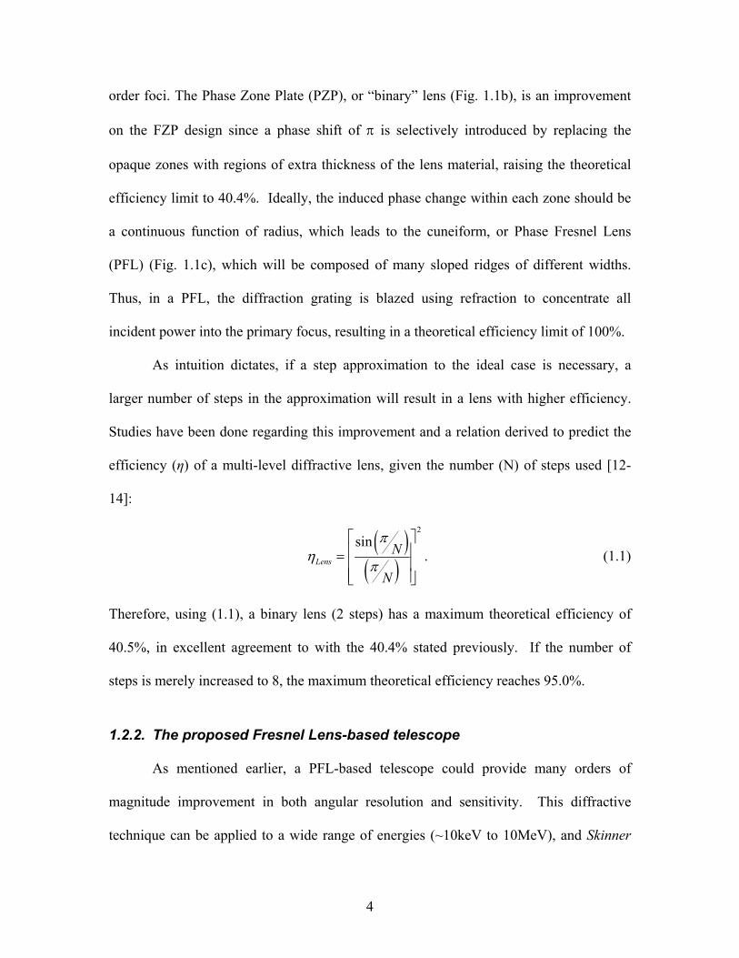
Invented by Soret in 1875, a Fresnel Zone Plate (FZP) (Fig. 1.1a) is a small
grating that will diffract incident radiation towards its focus. As the off-axis (radial)
distance is increased, higher deflection angles are required and thus the width of each
zone of the diffraction grating becomes smaller. Yet an FZP is limited to an efficiency of
10.1% because the alternating opaque zones block half of the incident radiation and not
all energy is transferred to the primary focus, some unfocused energy passes to higher
Fig. 1.1: (a) Fresnel Zone Plate (FZP). (b) Phase Zone Plate (PZP) or “binary” lens. (c) Phase Fresnel Lens (PFL).
(a)
(b)
(c)
4
order foci. The Phase Zone Plate (PZP), or “binary” lens (Fig. 1.1b), is an improvement
on the FZP design since a phase shift of π is selectively introduced by replacing the
opaque zones with regions of extra thickness of the lens material, raising the theoretical
efficiency limit to 40.4%. Ideally, the induced phase change within each zone should be
a continuous function of radius, which leads to the cuneiform, or Phase Fresnel Lens
(PFL) (Fig. 1.1c), which will be composed of many sloped ridges of different widths.
Thus, in a PFL, the diffraction grating is blazed using refraction to concentrate all
incident power into the primary focus, resulting in a theoretical efficiency limit of 100%.
As intuition dictates, if a step approximation to the ideal case is necessary, a
larger number of steps in the approximation will result in a lens with higher efficiency.
Studies have been done regarding this improvement and a relation derived to predict the
efficiency (η) of a multi-level diffractive lens, given the number (N) of steps used [12-
14]:
( )( )
2sin
LensN
N
πη
π
=
. (1.1)
Therefore, using (1.1), a binary lens (2 steps) has a maximum theoretical efficiency of
40.5%, in excellent agreement to with the 40.4% stated previously. If the number of
steps is merely increased to 8, the maximum theoretical efficiency reaches 95.0%.
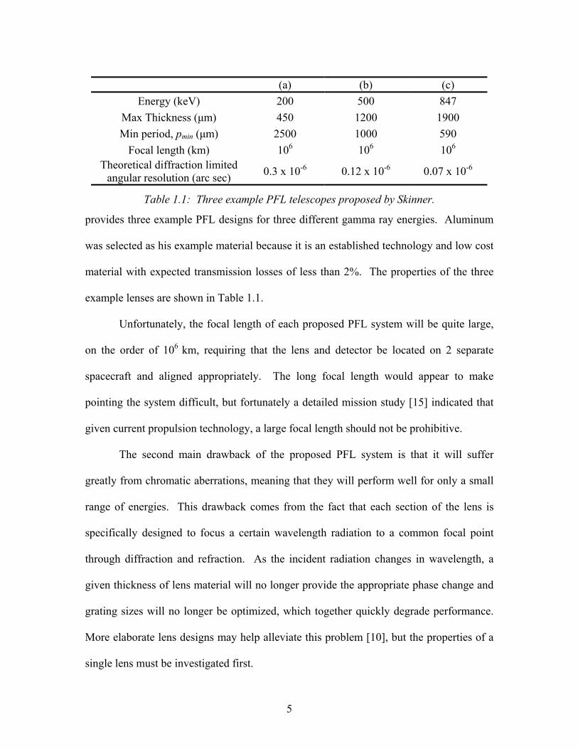
1.2.2. The proposed Fresnel Lens-based telescope
As mentioned earlier, a PFL-based telescope could provide many orders of
magnitude improvement in both angular resolution and sensitivity. This diffractive
technique can be applied to a wide range of energies (~10keV to 10MeV), and Skinner
5
provides three example PFL designs for three different gamma ray energies. Aluminum
was selected as his example material because it is an established technology and low cost
material with expected transmission losses of less than 2%. The properties of the three
example lenses are shown in Table 1.1.
Unfortunately, the focal length of each proposed PFL system will be quite large,
on the order of 106 km, requiring that the lens and detector be located on 2 separate
spacecraft and aligned appropriately. The long focal length would appear to make
pointing the system difficult, but fortunately a detailed mission study [15] indicated that
given current propulsion technology, a large focal length should not be prohibitive.
The second main drawback of the proposed PFL system is that it will suffer
greatly from chromatic aberrations, meaning that they will perform well for only a small
range of energies. This drawback comes from the fact that each section of the lens is
specifically designed to focus a certain wavelength radiation to a common focal point
through diffraction and refraction. As the incident radiation changes in wavelength, a
given thickness of lens material will no longer provide the appropriate phase change and
grating sizes will no longer be optimized, which together quickly degrade performance.
More elaborate lens designs may help alleviate this problem [10], but the properties of a
single lens must be investigated first.
(a) (b) (c) Energy (keV) 200 500 847
Max Thickness (µm) 450 1200 1900 Min period, pmin (µm) 2500 1000 590
Focal length (km) 106 106 106 Theoretical diffraction limited
angular resolution (arc sec) 0.3 x 10⁻⁶ 0.12 x 10⁻⁶ 0.07 x 10⁻⁶
Table 1.1: Three example PFL telescopes proposed by Skinner.
6
As stated earlier, the proposed PFL system should provide a 108 increase in
angular resolution and a 103 increase in sensitivity over current instruments. With this
increased angular resolution, the proposed PFL system will be ideally suited to observing
highly compact, and high surface brightness regions which cannot be sufficiently imaged
with current technology.
1.3. Test lens considerations
To first demonstrate the superior imaging properties of a PFL, a number of scaled
down lenses must be developed for ground testing at lower energies, such as X-rays.
NASA has proposed to carry out such testing at the Marshall Space Flight Center X-ray
Calibration Facility (XRFC) in Hunstville, Alabama. The X-ray source at XRFC is
located in a tunnel approximately 0.5km from the detector, with an access point to the
center section of the tunnel located 400m from the source (to ensure a relatively
collimated beam) and 118m from the detector. It is at this access point where a test lens
must be mounted. Assuming a tungsten target as the X-ray source, the strongest emission
lines of interest will be the L_alpha line at 8.4keV and the K_alpha line at 59.3keV. The
sections that follow will discuss the selection of the test lens material and the
approximate dimensions of a lens given the ground-based testing setup described above.
1.3.1. Material Selection
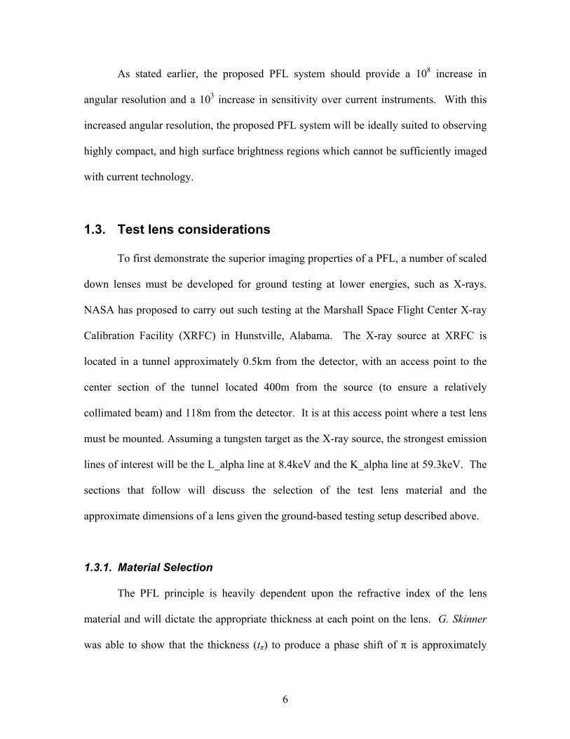
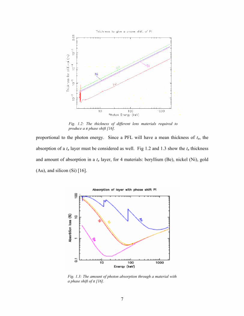
The PFL principle is heavily dependent upon the refractive index of the lens
material and will dictate the appropriate thickness at each point on the lens. G. Skinner
was able to show that the thickness (tπ) to produce a phase shift of π is approximately
7
proportional to the photon energy. Since a PFL will have a mean thickness of tπ, the
absorption of a tπ layer must be considered as well. Fig 1.2 and 1.3 show the tπ thickness
and amount of absorption in a tπ layer, for 4 materials: beryllium (Be), nickel (Ni), gold
(Au), and silicon (Si) [16].
Fig. 1.2: The thickness of different lens materials required to produce a π phase shift [16].
Fig. 1.3: The amount of photon absorption through a material with a phase shift of π [16].
8
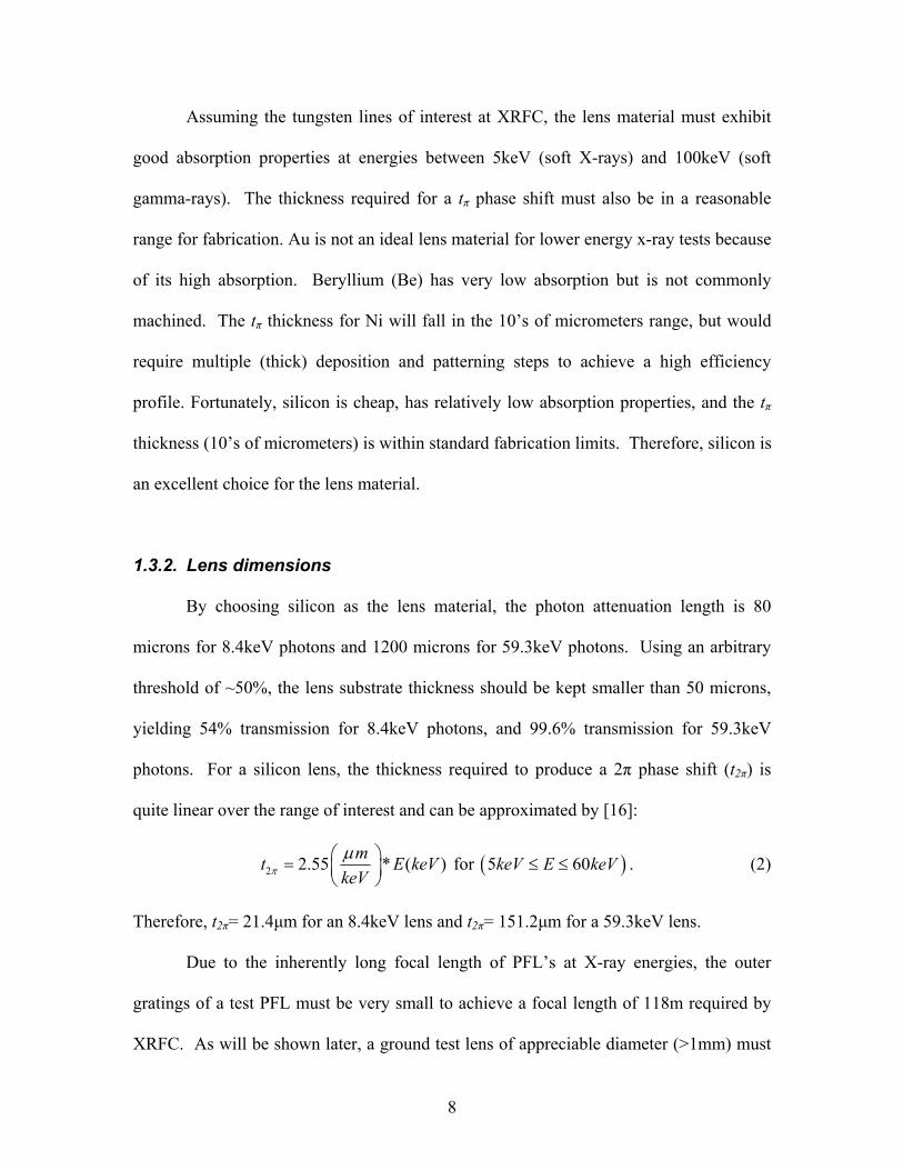
Assuming the tungsten lines of interest at XRFC, the lens material must exhibit
good absorption properties at energies between 5keV (soft X-rays) and 100keV (soft
gamma-rays). The thickness required for a tπ phase shift must also be in a reasonable
range for fabrication. Au is not an ideal lens material for lower energy x-ray tests because
of its high absorption. Beryllium (Be) has very low absorption but is not commonly
machined. The tπ thickness for Ni will fall in the 10’s of micrometers range, but would
require multiple (thick) deposition and patterning steps to achieve a high efficiency
profile. Fortunately, silicon is cheap, has relatively low absorption properties, and the tπ
thickness (10’s of micrometers) is within standard fabrication limits. Therefore, silicon is
an excellent choice for the lens material.
1.3.2. Lens dimensions
By choosing silicon as the lens material, the photon attenuation length is 80
microns for 8.4keV photons and 1200 microns for 59.3keV photons. Using an arbitrary
threshold of ~50%, the lens substrate thickness should be kept smaller than 50 microns,
yielding 54% transmission for 8.4keV photons, and 99.6% transmission for 59.3keV
photons. For a silicon lens, the thickness required to produce a 2π phase shift (t2π) is
quite linear over the range of interest and can be approximated by [16]:
2 2.55 * ( )mt E keVkeVπµ =
for ( )5 60keV E keV≤ ≤ . (2)
Therefore, t2π= 21.4µm for an 8.4keV lens and t2π= 151.2µm for a 59.3keV lens.
Due to the inherently long focal length of PFL’s at X-ray energies, the outer
gratings of a test PFL must be very small to achieve a focal length of 118m required by
XRFC. As will be shown later, a ground test lens of appreciable diameter (>1mm) must
9
then have outer ridge widths on the order of 10’s of micrometers, and it should be
reiterated that each of these ridges must have a unique sloped or stepped profile in order
to achieve a highly efficient PFL.
By choosing silicon as the material for the PFLs described above, we may take
advantage of the plethora of technologies available and under development in the area of
micro-fabrication, and specifically some fabrication technologies currently being
developed in the area of Micro-Electro-Mechanical Systems (MEMS).
1.4. Micro-Electro-Mechanical Systems (MEMS) Fabrication
Originating from the established fabrication methods of the integrated circuit (IC)
industry, the field of MEMS has grown tremendously over the past decade, as planar
processes, originally used to make transistors and diodes, were extended to make small
mechanical structures and “Microsystems.” Complicated layer structures and established
fabrication methods enabled many ‘macro-scale’ components to be mimicked or
improved on the ‘micro-scale.’ The possibility emerged for high performance, low
power, and low cost systems using similar batch fabrication techniques to those used in
the IC industry to fabricate many devices/systems simultaneously.
Many MEMS components use simple physical principles, such as electrostatic
actuation or capacitance, to create movement or sensing on a micrometer scale. Some of
the most common MEMS applications have come in accelerometers in cars. A
significant deceleration (possibly signifying a crash) can be sensed through a change in
capacitance from a small proof mass moving on a tiny silicon chip, deploying an airbag if
necessary. The field of MEMS has also grown to include areas of research with
10
applications in biotechnology (a ‘lab-on-a-chip’), optoelectronics (waveguides and
switches), power generation (micro-engines), and many more.
Research advances in MEMS fabrication can be applied to an ever increasing
range of devices and concepts that wish to take advantage of the batch fabrication,
potentially low cost, and high performance of devices made in the micrometer to
millimeter scale. The limits are constantly being pushed in both academia and industry
as the potential of MEMS is explored even further. The next sections will describe some
of the planar fabrication techniques used in MEMS, compare some Fresnel lenses
fabricated with such planar techniques, and discuss some of the 3D fabrication techniques
currently available and under development in MEMS.
1.4.1. Planar MEMS Fabrication
Since MEMS fabrication originated from planar IC processes, the basic planar
fabrication methods described below are quite well established and as such will not be
covered in great detail, nor should this discussion be considered a complete review of all
planar techniques used in IC fabrication. Similar fabrication principles can be applied to
other material substrates, such as III-V semiconductors, but only silicon is discussed here.
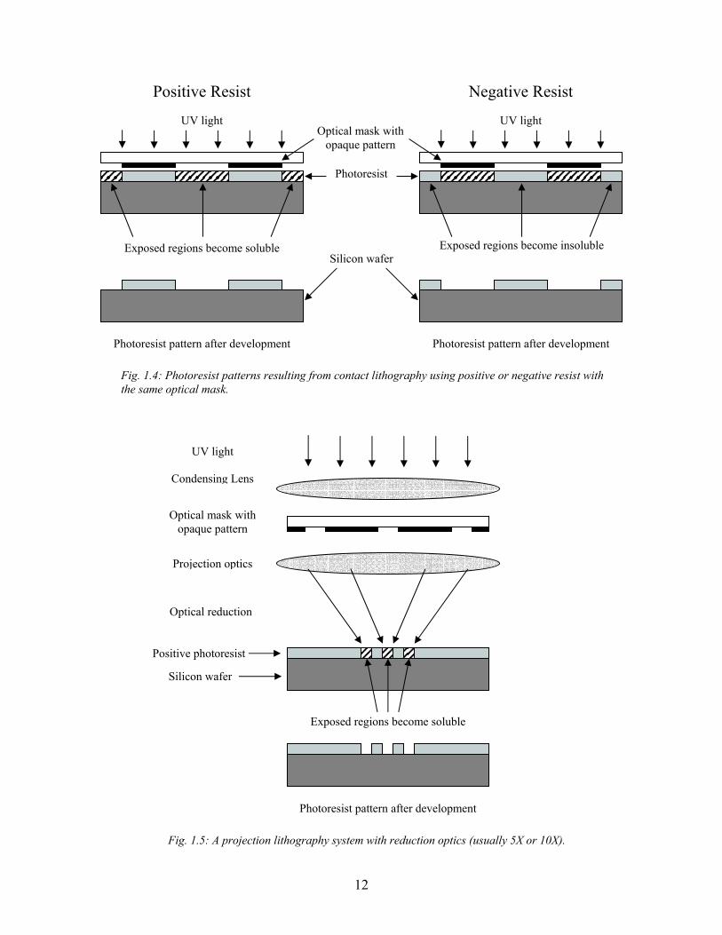
1.4.1.1. Photolithography
The general method used to define features on a wafer is termed
“photolithography.” The enabling material of photolithography, or lithography, is a
polymeric optically-sensitive material called “photoresist.” Thin photoresist films,
usually 1-5 µm thick, are deposited onto a silicon wafer through a spin-coating process.
11
The photoresist is then baked in a convection oven or on a hot plate at low temperature
(110ºC) to remove solvent. An optical photomask with clear and opaque patterns is then
used to selectively transmit incident UV light, exposing only those areas of photoresist
unprotected by an opaque section of the mask. Exposure to UV light will change the
chemistry of the photoresist, making it either more or less soluble in a developer solution.
If the photoresist is negative, areas exposed to UV light become cross-linked, and
insoluble in the developer solution, while the unexposed regions remain soluble.
Conversely, if the photoresist is positive, regions exposed to UV light have their bonds
broken and become more soluble than unexposed regions. Upon immersion in a
developing solution, soluble regions will be washed away and a spatially selective pattern
is formed in the photoresist, exposing certain regions of the wafer to further processing.
Figures 1.4 illustrates the photolithography process for negative and positive
photoresists in ‘contact’ lithography, where the optical mask is brought in contact or very
close proximity to the photoresist surface. Fig. 1.5 illustrates the principle of ‘projection’
lithography in which the optical mask is located above the photoresist surface and a series
of optics are used to transfer the pattern to the wafer in a step-and-repeat method. If
reduction optics are used, projection lithography systems may use optical masks that are
fabricated typically 4X, 5X, or 10X the dimensions desired on the wafer, making optical
masks inexpensive and small linewidths easier to achieve. Projection lithography
systems are primarily used in the IC industry, while contact lithography is often used in
MEMS fabrication because it can produce most required dimensions and contact systems
are less costly and easier to maintain.
12
Photoresist pattern after development Photoresist pattern after development
Silicon wafer
UV light
Exposed regions become soluble Exposed regions become insoluble
Positive Resist Negative Resist
Optical mask with opaque pattern
Photoresist
UV light
Fig. 1.4: Photoresist patterns resulting from contact lithography using positive or negative resist with the same optical mask.
Fig. 1.5: A projection lithography system with reduction optics (usually 5X or 10X).
Photoresist pattern after development
Silicon wafer
UV light
Exposed regions become soluble
Optical mask with opaque pattern
Positive photoresist
Condensing Lens
Projection optics
Optical reduction
13
Photolithography can also be accomplished through the use of an electron-beam,
or e-beam. By using an electron-beam photoresist material, usually poly-
methylmethacrylate (PMMA), areas exposed to the e-beam depolymerize and become
locally soluble, analogous to conventional lithography. However, e-beam lithography
has the advantage of being able to create fine resist patterns (on the order of 20nm) since
the electron beam/gun can be controlled with extreme accuracy. Unfortunately the
process is often slow as each individual pattern on a substrate must be written in a serial
manner rather than creating many patterns at once as is done in conventional lithography.
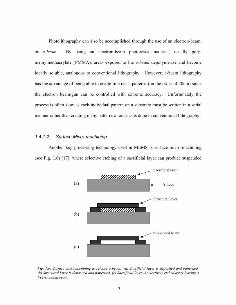
1.4.1.2. Surface Micro-machining
Another key processing technology used in MEMS is surface micro-machining
(see Fig. 1.6) [17], where selective etching of a sacrificial layer can produce suspended
(a)
(b)
(c)
Sacrificial layer
Structural layer
Silicon
Suspended beam
Fig. 1.6: Surface micromachining to release a beam. (a) Sacrificial layer is deposited and patterned. (b) Structural layer is deposited and patterned. (c) Sacrificial layer is selectively etched away leaving a free-standing beam.
14
structures. By first patterning a sacrificial layer, a structural layer may be deposited and
patterned on top. After selective removal of the sacrificial layer, a suspended structure
remains. With multiple deposition and etching steps, vertical structures may be extruded
from the silicon surface, creating stepped profiles with multiple steps. Figure 1.6 shows
the steps involved in releasing a suspended beam. However, surface micromachining is a
technique used primarily on deposited layers, while our test PFL structures should be
made out of a crystalline silicon substrate rather than deposited amorphous layers.
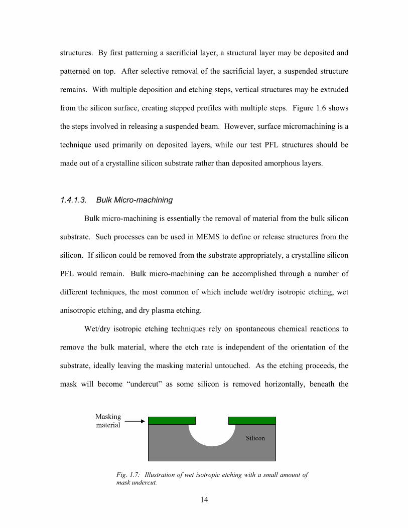
1.4.1.3. Bulk Micro-machining
Bulk micro-machining is essentially the removal of material from the bulk silicon
substrate. Such processes can be used in MEMS to define or release structures from the
silicon. If silicon could be removed from the substrate appropriately, a crystalline silicon
PFL would remain. Bulk micro-machining can be accomplished through a number of
different techniques, the most common of which include wet/dry isotropic etching, wet
anisotropic etching, and dry plasma etching.
Wet/dry isotropic etching techniques rely on spontaneous chemical reactions to
remove the bulk material, where the etch rate is independent of the orientation of the
substrate, ideally leaving the masking material untouched. As the etching proceeds, the
mask will become “undercut” as some silicon is removed horizontally, beneath the
Fig. 1.7: Illustration of wet isotropic etching with a small amount of mask undercut.
Silicon
Masking material
15
masking layer. See Fig 1.7. For silicon, a common chemistry includes vapor-phase
xenon-diflouride (XeF2), which can dissociate into many forms (XeF+, F+, etc) and the F+
atoms spontaneously react with the silicon to form a volatile (SiF4). This volatile then
desorbs from the silicon surface along with any residual xenon. Unfortunately, isotropic
etching is usually used for shallow applications (<5µm) and gives little control over the
etch profile, making it a poor fabrication technique to adopt for a test PFL in silicon.
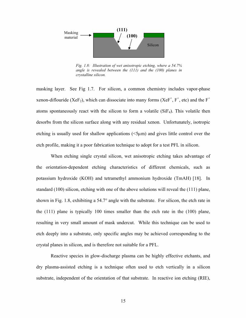
When etching single crystal silicon, wet anisotropic etching takes advantage of
the orientation-dependent etching characteristics of different chemicals, such as
potassium hydroxide (KOH) and tetramethyl ammonium hydroxide (TmAH) [18]. In
standard (100) silicon, etching with one of the above solutions will reveal the (111) plane,
shown in Fig. 1.8, exhibiting a 54.7° angle with the substrate. For silicon, the etch rate in
the (111) plane is typically 100 times smaller than the etch rate in the (100) plane,
resulting in very small amount of mask undercut. While this technique can be used to
etch deeply into a substrate, only specific angles may be achieved corresponding to the
crystal planes in silicon, and is therefore not suitable for a PFL.
Reactive species in glow-discharge plasma can be highly effective etchants, and
dry plasma-assisted etching is a technique often used to etch vertically in a silicon
substrate, independent of the orientation of that substrate. In reactive ion etching (RIE),
Fig. 1.8: Illustration of wet anisotropic etching, where a 54.7% angle is revealed between the (111) and the (100) planes in crystalline silicon.
(100) (111)
Silicon
Masking material
16
the most common dry etching technique for silicon (Si), a plasma is used to dissociate
and ionize a gas, such as carbon-tetraflouride (CF4) or sulfer-hexaflouride (SF6). A wafer
is then placed on an anode which is driven with a negative DC bias that accelerates the
ions towards the wafer surface.
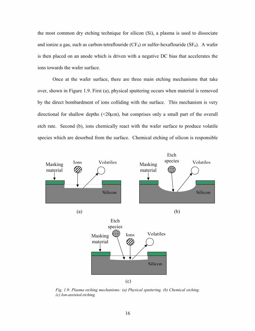
Once at the wafer surface, there are three main etching mechanisms that take
over, shown in Figure 1.9. First (a), physical sputtering occurs when material is removed
by the direct bombardment of ions colliding with the surface. This mechanism is very
directional for shallow depths (<20µm), but comprises only a small part of the overall
etch rate. Second (b), ions chemically react with the wafer surface to produce volatile
species which are desorbed from the surface. Chemical etching of silicon is responsible
Ions Volatiles
Silicon
Masking material
Etch species Volatiles
Silicon
Masking material
Silicon
Masking material
Etch species
VolatilesIons
(a) (b)
(c)
Fig. 1.9: Plasma etching mechanisms: (a) Physical sputtering. (b) Chemical etching. (c) Ion-assisted etching.
17
for the majority of the etch rate, and is usually achieved by ionizing a gas containing F,
such as CF4 or SF6. The third etch mechanism in RIE (c), often called ion-assisted
etching, a combination of the first two mechanisms whereby ion-bombardment damages
the silicon surface in order to make it more chemically reactive. This mechanism can
assist in creating vertical etch profiles as the incident ions damage the horizontal surface
of the substrate more than the sidewalls, increasing the etch rate vertically but not
horizontally.
RIE is widely used to remove silicon vertically from the substrate, and is a
potential candidate for removing silicon selectively from a bulk material for a PFL.
However, the PFL target depths being considered here (20 to 150µm) are beyond the
standard range of RIE (<20µm). A technique called deep reactive ion etching (DRIE) has
been developed [19] for applications, such as ours, requiring deeper etches. DRIE uses a
very similar process to that of RIE, however etching and passivation steps are cycled in a
high density plasma to provide a temporary protection of the silicon sidewall during
etching, enabling vertical sidewalls and deep etches (beyond 400µm). DRIE will be
discussed in more detail in Chapter 2 of this thesis.
1.4.1.4. Planar micro-scale Fresnel Lenses
To this point, X-ray microscopy has been the most common motivation for
fabricating Fresnel lenses, yet the dimensions of an astronomical test lens in silicon are
quite different than those designed for most X-ray microscopy applications.
Spector et al. [20] have fabricated FZP’s in both germanium (Ge) and nickel (Ni)
for photons in the 500eV range. Using e-beam lithography and electroplating, lenses
18
with diameters <200µm were fabricated with outer zone widths as small as 20nm. Since
the authors motivation was x-ray microscopy, each FZP emphasized spatial resolution
rather than angular resolution. Not only were these lenses for lower target energies than
those being considered in this thesis, but the lens diameters would be too small to collect
an appreciable number of photons from a distant x-ray source, such as the one at XRCF.
Chen et al. [21] were successful in fabricating a 1.8mm diameter gold (Au) FZP
for 8keV photons, much closer to the target energy and diameter of a test PFL in silicon.
The Au layer was reported to be 1.6µm, relatively thick for an Au layer in MEMS. Being
chiefly concerned with good spatial resolution, and short focal length (~3m), outer zone
widths were designed to be sub-micrometer. Fabrication was again accomplished using
e-beam lithography and electroplating. While the authors did achieve a large diameter x-
ray lens with sub-micron zone widths, the lens was still binary and made of Au, limiting
its maximum efficiency and having higher absorption than silicon. Also, to achieve
increased angular resolution, the dimensions of an FZP would change dramatically,
rendering most of the customized e-beam work done by the authors irrelevant.
DiFabrizio and Gentili [22] used a similar e-beam lithography and electroplating
approach as the authors mentioned above, however they chose to work towards higher
efficiency performances: namely developing a stepped PFL. Lenses of 150µm in
diameter were fabricated in both nickel (Ni) and gold (Au) with material layers <5µm
thick. Lenses were designed with 4 levels per zone for energies between 5 and 8keV,
again for x-ray microscopy applications concerned with spatial resolution. These lenses
were able to demonstrate efficiencies greater than the binary limit of 40%, however a test
19
PFL in silicon needs to be much larger in diameter and depth, while exhibiting low
absorption, high efficiency, and high angular resolution.
1.4.2. 3Dimensional MEMS Fabrication
It has been established thus far that the proposed test PFL in silicon must have
zone widths up to 100 times larger than those created previously and must also be much
thicker (>20µm) to achieve the appropriate phase shift over a range of energies.
Conventional planar MEMS fabrication methods merely extrude shapes from the
substrate with deposited layers, or remove material vertically or on crystalline planes.
However, the fabrication method used to create the PFL proposed for this research must
be somewhat unconventional to achieve this unique combination of size and
performance. Therefore, 3Dimensional MEMS fabrication methods must be explored.
Microstereolithography [23] is a method of creating 3D SU-8 (a photosensitive
polymer) molds by consecutively depositing and patterning many thin SU-8 layers one at
a time. Using many patterning steps, 3D structures can be made, but the process becomes
quite time consuming. Also, the approach is best suited to polymers and is not
appropriate for silicon applications such as our PFL.
3D metal structures have been achieved with angled sidewalls by using a rotating
light source in a customized lithography setup and then electroplating [24]. A rotating
light source exposes the desired film at an angle (through two separate masks) and upon
development and electroplating, an angled structure may be created. However, this
technique requires many customized instruments and again is geared towards fabrication
of 3D structures in materials other than silicon.
20
Other groups have directed ions in DRIE with buried dielectric layers [25] to
achieve angled etch sidewalls in silicon. This process requires the bonding of multiple
wafers with a charged dielectric between them. Upon etching through the dielectric,
charged ions are directed away from the dielectric layer creating angled etching
characteristics. However, the authors state that the etch results are not always repeatable,
and the bonding of multiple wafers is often avoided due to processing complications.
Ideally, a test PFL in silicon should be fabricated using a method that creates the
entire 3D structure at one time, eliminating all alignment steps. This fabrication method
must also achieve a wide range of vertical and horizontal dimensions, allowing each zone
of a PFL to be individually contoured to maximize lens efficiency.
Recently, an alternative method of fabricating 3D structures, called “Gray-scale
technology,” has been investigated as a MEMS fabrication method [26]. 3D structures
with stepped profiles and horizontal dimensions ranging from 5µm to 20mm are created
in a single lithography step, yielding a controllable profile in photoresist. This
photoresist pattern may then be used as a nested mask in a dry-anisotropic etching
process, such as RIE or DRIE, to selectively transfer the 3D photoresist profile into a 3D
silicon structure. Since our target depths are beyond the normal limits of standard RIE,
DRIE can be used as the transfer technique, where etch depths greater than >20µm can be
easily achieved.
Gray-scale technology has thus been chosen as the fabrication technique to be
used in this research to develop a high efficiency, high angular resolution PFL in silicon.
Gray-scale technology will be presented in detail in Chapter 2 of this thesis, while
Chapter 3 will discuss design considerations for gray-scale optical masks and introduce a

21
novel method for predicting the 3D photoresist profiles of various PFLs. Chapter 4 will
summarize the lithography and etching results achieved while fabricating test PFLs, and
evaluate the resulting silicon profiles. Concluding remarks about the use of gray-scale
technology for fabricating test PFLs in silicon will be provided in Chapter 5, and some
future work on silicon PFLs and gray-scale technology will be discussed.
22
2. Gray-scale Technology
2.1. Introduction
Previously, gray-scale lithography has been widely utilized in the area of
diffractive optics [27-29]. However, gray-scale technology using dry-anisotropic etching
has recently emerged as an enabling fabrication method for creating 3D structures for
MEMS applications [30,31]. For clarity, the term ‘gray-scale lithography’ will refer to a
photolithography process using a ‘gray-scale optical mask,’ while the term ‘gray-scale
technology’ will refer to the combination of ‘gray-scale lithography’ and a dry-
anisotropic etching step to transfer the photoresist pattern into the silicon.
Gray-scale mask design and lithography can be approached in a number of ways,
however all methods rely on the same general principles [26,32-35]. A gray-scale optical
mask is used to transmit only a portion of the incident intensity of light, partially
exposing sections of a positive photoresist to a certain depth. This exposure renders the
top portion of the photoresist layer more soluble in a developer solution, while the bottom
portion of the photoresist layer remains unchanged. Therefore, after a standard
development step, some thickness of photoresist, called a ‘gray level,’ will remain behind
in areas that received a partial exposure. By locally modulating this intensity pattern
with a specially designed gray-scale optical mask, many gray levels may be created at
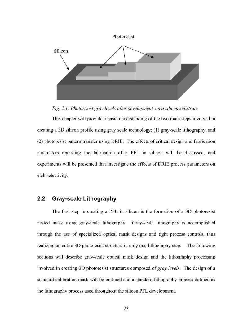
once, forming a 3D structure in the photoresist (see Fig. 2.1). By patterning the
photoresist on a silicon wafer, a dry-anisotropic etching technique, such as reactive ion
etching (RIE) or deep reactive ion etching (DRIE), may be used to subsequently transfer
this pattern into the silicon.
23
This chapter will provide a basic understanding of the two main steps involved in
creating a 3D silicon profile using gray scale technology: (1) gray-scale lithography, and
(2) photoresist pattern transfer using DRIE. The effects of critical design and fabrication
parameters regarding the fabrication of a PFL in silicon will be discussed, and
experiments will be presented that investigate the effects of DRIE process parameters on
etch selectivity.
2.2. Gray-scale Lithography
The first step in creating a PFL in silicon is the formation of a 3D photoresist
nested mask using gray-scale lithography. Gray-scale lithography is accomplished
through the use of specialized optical mask designs and tight process controls, thus
realizing an entire 3D photoresist structure in only one lithography step. The following
sections will describe gray-scale optical mask design and the lithography processing
involved in creating 3D photoresist structures composed of gray levels. The design of a
standard calibration mask will be outlined and a standard lithography process defined as
the lithography process used throughout the silicon PFL development.
Fig. 2.1: Photoresist gray levels after development, on a silicon substrate.
Silicon
Photoresist
24
2.2.1. Gray-scale mask design
The chosen method of gray-scale patterning, as detailed by Waits et al. [26,32]
uses various sized opaque features, called ‘pixels’ on a transparent background. These
pixels block a fraction of the incident light and cause diffraction as the light passes
between them. The light transmitted between pixels can be modeled as the transmission
of a square wave function. By expanding this square wave into a Fourier series [36], it
can be seen that the 0th diffraction order acts as a ‘DC’ component to the transmitted
light, while all higher diffraction orders are spatial frequency terms that depend on the
spatial dimensions of the features on the mask. By recalling the elements of a projection
lithography system (Fig. 1.6), the objective lens serves to collect the diffracted light from
the optical mask and transmit it through the system to the wafer. As the spatial
dimensions of opaque features on the optical mask are decreased, the higher diffraction
orders become spread out in the plane of the objective lens. Once the pixels and their
spacing are below the resolution of the chosen projection lithography system, only the 0th
diffraction order is collected by the objective lens, effectively truncating the Fourier
series leaving only the ‘DC’ component to the transmitted light [26]. The resolution of
the stepper system may be approximated as [37]:
( )1Resolution
NAλσ
=+
(2.1)
where σ is the partial coherence of the light source, NA is the numerical aperture,
and λ is the wavelength of light being used. By varying the size of the sub-resolution
pixels, this ‘DC’ component of the transmission can be locally modulated, resulting in the
exposure of a photoresist film to various depths.
25
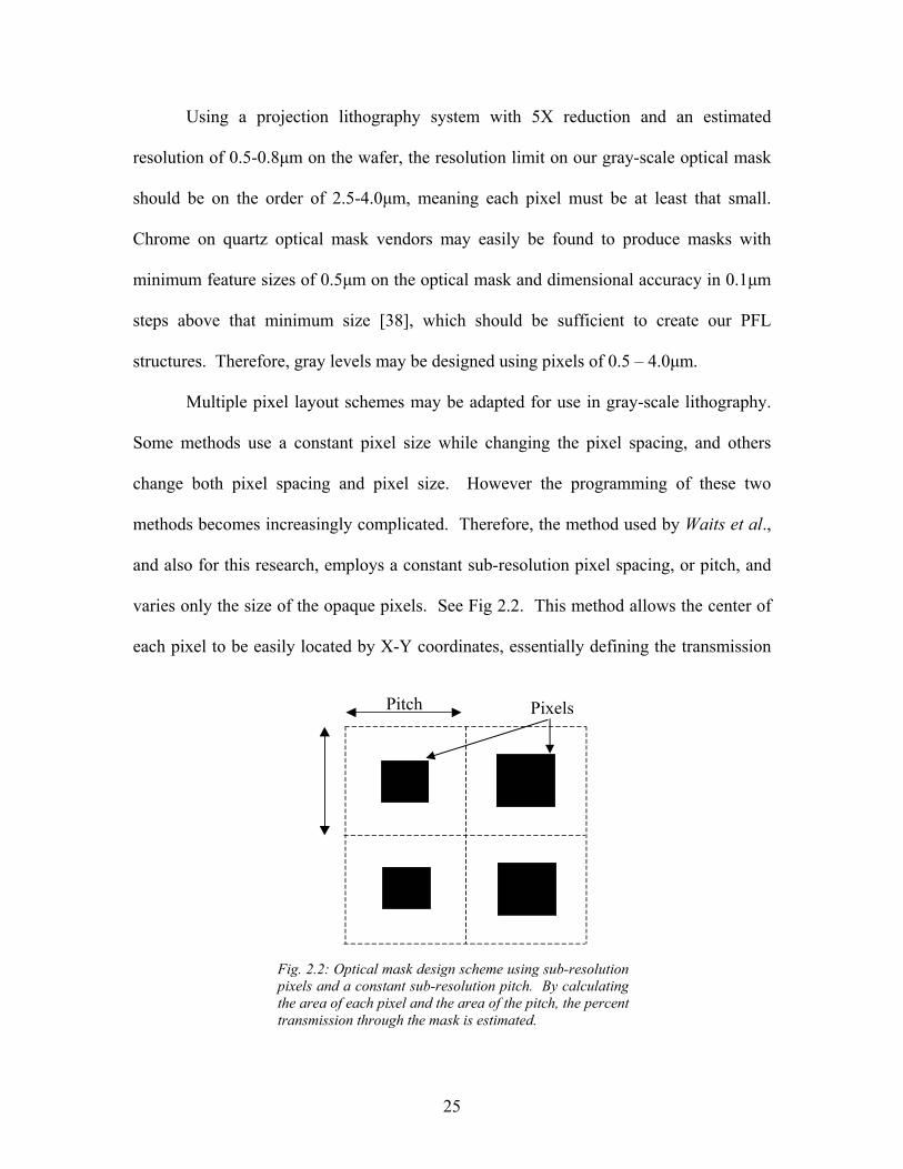
Using a projection lithography system with 5X reduction and an estimated
resolution of 0.5-0.8µm on the wafer, the resolution limit on our gray-scale optical mask
should be on the order of 2.5-4.0µm, meaning each pixel must be at least that small.
Chrome on quartz optical mask vendors may easily be found to produce masks with
minimum feature sizes of 0.5µm on the optical mask and dimensional accuracy in 0.1µm
steps above that minimum size [38], which should be sufficient to create our PFL
structures. Therefore, gray levels may be designed using pixels of 0.5 – 4.0µm.
Multiple pixel layout schemes may be adapted for use in gray-scale lithography.
Some methods use a constant pixel size while changing the pixel spacing, and others
change both pixel spacing and pixel size. However the programming of these two
methods becomes increasingly complicated. Therefore, the method used by Waits et al.,
and also for this research, employs a constant sub-resolution pixel spacing, or pitch, and
varies only the size of the opaque pixels. See Fig 2.2. This method allows the center of
each pixel to be easily located by X-Y coordinates, essentially defining the transmission
Fig. 2.2: Optical mask design scheme using sub-resolution pixels and a constant sub-resolution pitch. By calculating the area of each pixel and the area of the pitch, the percent transmission through the mask is estimated.
Pitch
Pixels
26
at that point on the mask. Since each pixel is sub-resolution, the actual shape of the pixel
should not be reconstructed and therefore only the total area of the pixel will be
important. For this research, rectangular pixels were used to make mask design and
fabrication as simple as possible.
It is then useful to calculate the relative amount of light blocked by the opaque
pixel, or equivalently the percentage of light transmitted through the optical mask. By
calculating the area of each pixel (Apixel) and the area of the square pitch (Apitch), we can
estimate the percent transmission through the optical mask (Tr) as:
1 pixel
pitch
ATr
A= − . (2.2)
Mask fabrication provides some constraints on pixel dimensions and their possible
increments, so the choice of a mask pitch immediately dictates the upper and lower
bounds of Tr. The number of different size rectangles that may be created between these
limits will be finite. The result is a discrete Tr set that depends on the selected pitch and
the mask vendor limitations, with each Tr creating a distinct gray level in photoresist.
2.2.2. Lithography Processing
Once mask design and fabrication is complete, a gray-scale lithography process
must be created. Traditionally, exposed photoresist is either totally cleared or entirely
left behind, depending on its polarity (positive or negative). The goal of gray-scale
lithography is to only clear away a fraction of the photoresist thickness, leaving behind a
series of gray levels that together form a 3D photoresist structure. The partial light
transmission through the specially designed gray-scale optical mask coupled with time of
exposure, time of development, and photoresist contrast, will determine these final
27
intermediate gray level heights in photoresist. The lithography processing for this
research was performed by a collaborator on this research, C. Michael Waits, on a 5X
projection lithography system (CGA-Ultratech) in the clean-room facilities at the
Laboratory for Physical Sciences (LPS), in College Park, MD. Further details on the
gray-scale lithography process may be found in [26].
2.2.2.1. Photoresist Selection
Gray-scale lithography processing begins with the spinning of a thin photoresist
film onto a silicon wafer. In the case of this research, 75mm <100> test grade silicon
wafers were used for compatibility with the projection lithography system at LPS.
However, photoresists used in gray-scale lithography may have some properties that
differ from high-resolution photoresists used in other applications. Typically, gray-scale
lithography uses photoresists that exhibit low ‘contrast,’ where contrast is essentially a
measure of how sensitive the photoresist is to changes in exposure dose.
Ideally, as the exposure dose is increased on a photoresist with the highest
possible contrast, there will be one point at which the photoresist changes from
unexposed to totally exposed, usually referred to as the ‘clearing dose.’ However, no
photoresist exhibits this ideal clearing dose behavior, every photoresist has a small
exposure dose ‘range’ in which the photoresist will be partially removed during
development. The contrast of a photoresist is defined as the slope of the development
rate vs. log(exposure dose) curve, and essentially measures the size of this ‘range.’
Photoresists with low contrast should realize more gray levels because a large portion of
the available Tr values from the mask design will fit inside the operating range, enabling
28
a larger number of achievable gray levels. Photoresists with high contrast behave closer
to the ideal case, making the operating range for gray-scale lithography quite small.
Additionally, thicker photoresists are better suited to gray-scale lithography
because the gray levels may be more pronounced and a larger margin of error afforded to
the process. Clariant’s AZ9245 was chosen as the photoresist for this research because it
has relatively low contrast and can be spun to a nominal thickness of >6µm with ease.
The spin coating procedure is followed by a 90 sec soft bake step at 110°C to remove
solvent. No hard bake step is required according to the manufacturer.
2.2.2.2. Exposure
To find the optimum exposure dose for gray-scale lithography, a focus-exposure
matrix must be performed, as is done in conventional lithography. In a focus exposure
matrix, the exposure dose is varied along the rows and the focus is varied along the
columns of the dies on a wafer, giving many combinations of focus and exposure. By
inspection, the die with the best results will then determine the optimum settings for both
the focus and exposure. However, the evaluation of the exposure results after a fixed
development step is different if your purposes are gray-scale in nature. In gray-scale
lithography, it is desirable to find the exposure dose where the fully exposed photoresist
is barely removed; ensuring the largest possible range for gray levels. To evaluate this
optimum exposure point, visual inspection determines when the photoresist is fully
cleared away in open areas. The number of gray levels remaining on a calibration
structure containing a wide range of gray levels can then be counted. (The design and
properties of such a calibration optical mask will be discussed in section 2.2.3.) The die
29
with the largest number of gray levels remaining after development is interpreted to have
the exposure settings closest to ideal for gray-scale lithography processing.
2.2.2.3. Development
The one element that has been taken as a given until this point has been the
development step. During photoresist development, even areas of unexposed photoresist
will be removed, albeit extremely slowly. Depending on the time of development, areas
receiving any exposure dose will eventually develop fully. By inspection an appropriate
development range can be established, but in this range there are multiple development
recipes that yield many gray levels. Depending on previous processing steps, different
development recipes may appear ideal, but for this research, the development step is held
constant, and gray-scale structures are optimized primarily through optical mask design.
During development, the concentration of developer solution and the time
necessary for development are inversely proportional. The developer solution used for
this research was Clariant’s AZ400K, mixed in a concentration of 3:1, DI water to
developer solution. This yielded development times in the 3-5 minute range, much
longer than conventional development times of 1-2 minutes. Using a stronger
concentration of developer solution may decrease the development time, but the faster
development rate will make it more difficult to stop the development at the appropriate
time. If over-development occurs, there will be a loss of lower gray levels, and all
remaining gray levels will be lower than expected. The converse is also true, where
under-development will cause gray levels to be higher than expected and open areas may
not be fully developed. Fig. 2.3 shows three gray-scale stepped wedge structures. Fig.
30
2.3(a) shows a structure which has been over-developed and has lost the lowest of 4 gray
levels, while the remaining 3 gray levels are lower than expected. Fig. 2.3 (b) shows a
structure which has been under-developed where all gray levels are higher than expected
and the open areas were not fully cleared away. Fig. 2.3 (c) shows a structure developed
for the appropriate amount of time. When developing a precise silicon PFL, all gray
levels must be consistently achieved at the same height to ensure profile accuracy,
enabling high lens performance. Therefore, a longer development time must be tolerated
for high quality gray-scale structures like the PFL being developed in this research.
(a)
(b)
(c)
Fig. 2.3: A photoresist gray-scale wedge structure after (a) over-development, (b) under-development, and (c) appropriate development.
Photoresist
Silicon
31
2.2.3. Calibration mask
A generic calibration mask was created to experimentally investigate the
resolution of the projection lithography system being used. Gray-scale wedge structures
(like those shown in Fig. 2.2) were designed with various pitches ranging from 1.5µm to
4.0µm in 0.1µm increments to cover the estimated resolution range of 2.5-4.0µm pitch on
the optical mask. Using only square pixels, gray levels of fixed length (50-100µm) were
designed adjacent to each other. By using a combination of pitches and pixels, an
achievable range of pixels can be established for a wide range of pitches simultaneously.
An opaque area on the mask was included adjacent to the highest gray level as a
reference point, so the heights of gray levels after fabrication can be measured and
correlated to the pixel size that created them. Using scanning electron micrographs
(SEM) and optical microscopes, gray levels in photoresist were inspected to obtain the
resolution of the projection lithography system. See Fig. 2.4. Gray levels created by
over-resolution pitches appear rough as the tiny pixels are partially resolved in the
photoresist, see Fig. 2.4(a). Gray levels created by using sub-resolution pitches will
Fig. 2.4: SEM images showing two gray levels produced using two different pitches on the gray-scale mask; (a) shows a pitch slightly above resolution and (b) shows a smoother photoresist surface using a pitch right at the resolution limit.
(a) (b)
32
appear smooth, see Fig. 2.4(b). The resolution of the system is defined here to be the
largest mask pitch that still creates a smooth gray level. The pitch determined as the
resolution limit for our 5X reduction projection lithography system was 2.8µm, meaning
a horizontal resolution of ~0.56µm could be expected on the wafer for a photoresist PFL.
One major constraint that arises from the use of a 5X reduction system pertains to
the exposure area. When using a traditional 100mm optical mask plate, after 5X
reduction the exposed area will be only 20mm by 20mm, limiting the area that can be
patterned at one time. While this exposure area should be sufficient for most ground test
lenses, this limitation may prohibit this technology from being extended to space-bound
applications with much larger single lens dimensions.
The advantage of using a calibration mask to experimentally obtain a lithography
system’s gray-scale properties is that the many factors that determine the success of gray-
scale lithography can be simultaneously investigated by looking only at the final gray-
scale photoresist structures. Table 2.1 describes the wedge structures included on the
calibration mask designed for this research and described above.
Structure Pitch Largest Pixel (um) # of levels
Level Length (um)
D1 1.2 0.7 4 100 D2 1.3 0.8 5 50 D3 1.4 0.9 6 50 D4 1.5 1.0 7 50 D5 1.6 1.1 8 100 D6 1.7 1.2 9 50 D7 1.8 1.3 10 50 D8 1.9 1.4 11 50 D9 2.0 1.5 12 100
D10 2.1 1.6 13 50 D11 2.2 1.7 14 50 D12 2.3 1.8 15 50 D13 2.4 1.9 16 100 D14 2.4 1.9 16 100 D15 2.5 2.0 17 50
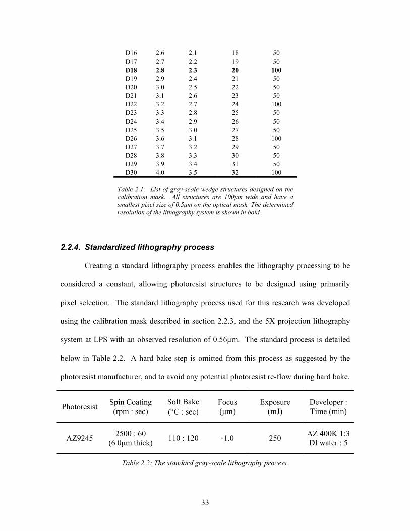
33
D16 2.6 2.1 18 50 D17 2.7 2.2 19 50 D18 2.8 2.3 20 100 D19 2.9 2.4 21 50 D20 3.0 2.5 22 50 D21 3.1 2.6 23 50 D22 3.2 2.7 24 100 D23 3.3 2.8 25 50 D24 3.4 2.9 26 50 D25 3.5 3.0 27 50 D26 3.6 3.1 28 100 D27 3.7 3.2 29 50 D28 3.8 3.3 30 50 D29 3.9 3.4 31 50 D30 4.0 3.5 32 100
Table 2.1: List of gray-scale wedge structures designed on the calibration mask. All structures are 100µm wide and have a smallest pixel size of 0.5µm on the optical mask. The determined resolution of the lithography system is shown in bold.
2.2.4. Standardized lithography process
Creating a standard lithography process enables the lithography processing to be
considered a constant, allowing photoresist structures to be designed using primarily
pixel selection. The standard lithography process used for this research was developed
using the calibration mask described in section 2.2.3, and the 5X projection lithography
system at LPS with an observed resolution of 0.56µm. The standard process is detailed
below in Table 2.2. A hard bake step is omitted from this process as suggested by the
photoresist manufacturer, and to avoid any potential photoresist re-flow during hard bake.
Photoresist Spin Coating (rpm : sec)
Soft Bake (°C : sec)
Focus (µm)
Exposure (mJ)
Developer : Time (min)
AZ9245 2500 : 60 (6.0µm thick) 110 : 120 -1.0 250 AZ 400K 1:3
DI water : 5
Table 2.2: The standard gray-scale lithography process.
34
2.3. Dry-anisotropic Etching
Once a photoresist gray-scale structure has been created, the pattern must be
transferred into the silicon via a selective etching process. As mentioned in section
1.4.1.3, deep reactive ion etching (DRIE) will be the preferred method of pattern transfer
for creating a silicon PFL to achieve the desired dimension range of 20 to 150 µm. The
DRIE system used in this research was a Unaxis, PlasmaTherm 770 Inductively Coupled
Plasma (ICP) etching system located in the clean-room at the Army Research Laboratory
(ARL) in Adelphi, MD.
2.3.1. Deep Reactive Ion Etching (DRIE)
Robert Bosch GmbH established the basic DRIE process in 1996 [19], while
Whitley et al. [39] briefly demonstrated and received a patent on the transfer of gray-scale
structures into silicon using DRIE in 2002. A basic DRIE process is shown in Fig. 2.5.
First, a masking material (often photoresist) is patterned; exposing only selected areas for
etching, see Fig. 2.5(a). The etching step is executed first using an inductively coupled
plasma (ICP) containing SF6 and Ar gases, which enables relatively vertical sidewalls
over small depths (usually ~1µm), however there will be a limited amount of isotropic
lateral etching of the silicon, see Fig. 2.5(b). C4F8 gas is then cycled into the chamber as
part of a passivation step, creating a conformal teflon-like film over the entire surface, see
Fig. 2.5(c). When the etching step is repeated, the passivation layer is preferentially
removed from horizontal surfaces by the Ar+ ions in the plasma allowing the vertical
etching to continue, while the previously etched silicon sidewall is temporarily protected
from continued etching by F ions, see Fig. 2.5(d). Passivation, Fig. 2.5(e) and etching,
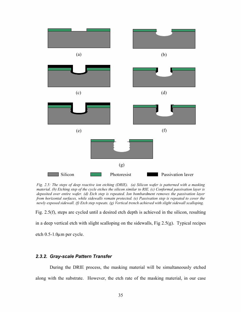
35
Fig. 2.5(f), steps are cycled until a desired etch depth is achieved in the silicon, resulting
in a deep vertical etch with slight scalloping on the sidewalls, Fig 2.5(g). Typical recipes
etch 0.5-1.0µm per cycle.
2.3.2. Gray-scale Pattern Transfer
During the DRIE process, the masking material will be simultaneously etched
along with the substrate. However, the etch rate of the masking material, in our case
(a)
(g)
(f) (e)
(c) (d)
(b)
Fig. 2.5: The steps of deep reactive ion etching (DRIE). (a) Silicon wafer is patterned with a masking material. (b) Etching step of the cycle etches the silicon similar to RIE. (c) Conformal passivation layer is deposited over entire wafer. (d) Etch step is repeated. Ion bombardment removes the passivation layer from horizontal surfaces, while sidewalls remain protected. (e) Passivation step is repeated to cover the newly exposed sidewall. (f) Etch step repeats. (g) Vertical trench achieved with slight sidewall scalloping.
Silicon Photoresist Passivation layer
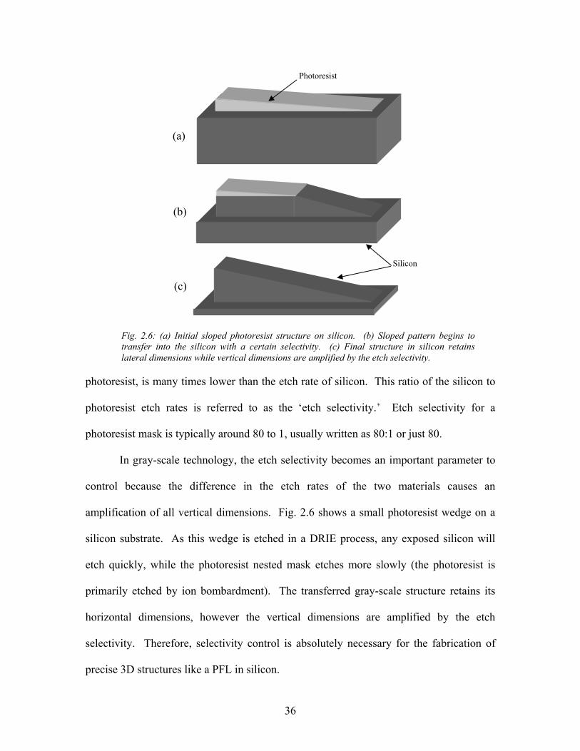
36
photoresist, is many times lower than the etch rate of silicon. This ratio of the silicon to
photoresist etch rates is referred to as the ‘etch selectivity.’ Etch selectivity for a
photoresist mask is typically around 80 to 1, usually written as 80:1 or just 80.
In gray-scale technology, the etch selectivity becomes an important parameter to
control because the difference in the etch rates of the two materials causes an
amplification of all vertical dimensions. Fig. 2.6 shows a small photoresist wedge on a
silicon substrate. As this wedge is etched in a DRIE process, any exposed silicon will
etch quickly, while the photoresist nested mask etches more slowly (the photoresist is
primarily etched by ion bombardment). The transferred gray-scale structure retains its
horizontal dimensions, however the vertical dimensions are amplified by the etch
selectivity. Therefore, selectivity control is absolutely necessary for the fabrication of
precise 3D structures like a PFL in silicon.
Fig. 2.6: (a) Initial sloped photoresist structure on silicon. (b) Sloped pattern begins to transfer into the silicon with a certain selectivity. (c) Final structure in silicon retains lateral dimensions while vertical dimensions are amplified by the etch selectivity.
(a)
(c)
(b)
Photoresist
Silicon
37
2.3.3. Selectivity control experiments
To investigate the etch properties of the DRIE system being utilized at ARL, a
series of experiments were used to gauge the effects of individual parameter changes in
the different DRIE process steps [31]. Samples were prepared with opaque and gray-
scale photoresist test structures on 75mm <100> test-grade silicon wafers. Each sample
wafer was then etched for 150 cycles, while individual etch parameters were varied
during each run. The etch recipe used as the starting point in this characterization, ‘Base
Etch I,’ is shown in Table 2.3.
Step Ar (sccm)
C4F8 (sccm)
SF6 (sccm)
Pressure (mTorr)
Water Temp(°C)
Electrode Power (W)
Time (sec)
Passivation 40 70 0 19 20 1 5
Etch 40 0 100 19 20 10 8
Table 2.3: DRIE process parameters for Base Etch I.
Three parameters were initially chosen to investigate the characteristics of our
DRIE tool: global silicon loading, electrode power, and chamber temperature (as
determined by the temperature of the water flowing through the chamber walls). Each
successive etch differed from Base Etch I in only one respect so that the effects of each
parameter could be isolated. The silicon loading of Base Etch I was 41%, while Base
Etch II had a silicon loading of 27% and Base Etch III had a silicon loading of 52%. The
high electrode power etch was done with a power of 12W during the etch step, while the
low electrode power etch had a power of 8W. The increased chamber temperature etch
was done with the water temperature set to 50°C instead of 20°C.
38
Height measurements of gray-scale structures at 5 points on each wafer were
taken in photoresist (before etching) and in silicon (after etching) to obtain the selectivity
resulting from the particular etch recipes:
tPhotoresis
Silicon
HH
ySelectivit = . (2.3)
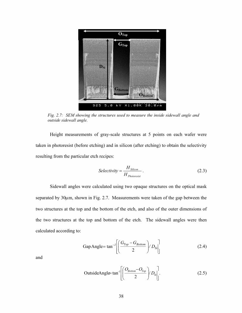
Sidewall angles were calculated using two opaque structures on the optical mask
separated by 30µm, shown in Fig. 2.7. Measurements were taken of the gap between the
two structures at the top and the bottom of the etch, and also of the outer dimensions of
the two structures at the top and bottom of the etch. The sidewall angles were then
calculated according to:
−= −
SiBottomTop1 D/
GG2
tanAngle Gap (2.4)
and
−= −
SiTopBottom D
OO/
2tanAngle Outside 1 . (2.5)
GTop
OTop
GBottom OBottom
Fig. 2.7: SEM showing the structures used to measure the inside sidewall angle and outside sidewall angle.
DSi
39
By calculating the angle in this way, re-entrant profiles will result in negative sidewall
angles and positive profiles will result in positive sidewall angles.
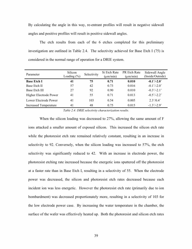
The etch results from each of the 6 etches completed for this preliminary
investigation are outlined in Table 2.4. The selectivity achieved for Base Etch I (75) is
considered in the normal range of operation for a DRIE system.
Parameter Silicon Loading (%) Selectivity Si Etch Rate
(µm/min) PR Etch Rate
(µm/min) Sidewall Angle (Inside/Outside)
Base Etch I 41 75 0.71 0.010 -0.1˚/-2.0˚ Base Etch II 57 42 0.73 0.016 -0.1˚/-2.0˚ Base Etch III 27 92 0.90 0.010 -0.3˚/-2.1˚ Higher Electrode Power 41 55 0.71 0.013 -0.5˚/-2.2˚ Lower Electrode Power 41 103 0.54 0.005 2.3˚/0.4˚ Increased Temperature 41 48 0.75 0.015 -1.3˚/-2.9˚
Table 2.4: DRIE selectivity characterization results. When the silicon loading was decreased to 27%, allowing the same amount of F
ions attacked a smaller amount of exposed silicon. This increased the silicon etch rate
while the photoresist etch rate remained relatively constant, resulting in an increase in
selectivity to 92. Conversely, when the silicon loading was increased to 57%, the etch
selectivity was significantly reduced to 42. With an increase in electrode power, the
photoresist etching rate increased because the energetic ions sputtered off the photoresist
at a faster rate than in Base Etch I, resulting in a selectivity of 55. When the electrode
power was decreased, the silicon and photoresist etch rates decreased because each
incident ion was less energetic. However the photoresist etch rate (primarily due to ion
bombardment) was decreased proportionately more, resulting in a selectivity of 103 for
the low electrode power case. By increasing the water temperature in the chamber, the
surface of the wafer was effectively heated up. Both the photoresist and silicon etch rates
40
increased, however the photoresist etch rate grew proportionately more resulting in a net
lowering of the selectivity to 48.
The sidewall profiles for the final 3 etches were considerably different from the
three Base etches, which were all fairly vertical. It should be noted that the outside angle
is consistently more re-entrant than the inside angle because the outside walls of the
structures being considered are subject to greater bombardment from ions with high
incident angles, whereas the inside walls are protected from highly angular incident ions
by the structure itself. In the high electrode power case, the increased energy of each
incident ion caused faster removal of the sidewall passivation layer, allowing slight
horizontal etching during each cycle, which in turn results in a more re-entrant profile
when compared to Base Etch I. Conversely, when the electrode power was lowered, the
sidewall passivation is not completely removed during each cycle causing a gradual
build-up of the passivation layer, resulting in a slightly positive profile (again being more
positive in the gap due to the decreased angular ion bombardment). When the chamber
temperature was increased, the rate of reactions involving the sidewall passivation layer
increased. This increased temperature caused the sidewall passivation layer to be
removed prematurely, resulting in a highly re-entrant sidewall profile.
This DRIE characterization enables recipes to be developed for tuning etch
selectivity to the desired values for etching a PFL in silicon. The effects of changing
individual parameters may be anticipated as they pertain to both etch selectivity and
sidewall profile. By combining multiple parameter changes and adjusting the passivation
layer thickness (length of passivation step), highly vertical etches with precise etch
selectivity are possible over a wide range of etch selectivities.
41
2.4. Summary
The goal of this chapter was to introduce in detail gray-scale lithography and 3D
photoresist pattern transfer using DRIE. The terms and concepts presented herein will be
used freely throughout chapters 3, 4, and 5 of this thesis as the specific design and
fabrication steps taken to achieve a PFL in silicon are described. Limitations imposed by
the chosen method of gray-scale patterning, such as horizontal resolution and maximum
exposure area, have been discussed as they pertain to the creation of a PFL in silicon, and
a preliminary DRIE characterization completed towards the creation of vertical etch
profiles with precisely controlled etch selectivity.
42
3. Optical Mask Design 3.1. Introduction
The proper design of a gray-scale optical mask is the single most important step
when creating a 3D structure. No matter how well the lithography and etching steps are
controlled, if the initial intensity pattern is incorrect, all subsequent processing is
pointless. It has been established that the chosen pixilation scheme will use a set of sub-
resolution pixels spaced on a sub-resolution pitch (section 2.2.1), however the selection
of exactly which pixels and which pitch to use depends on many factors when developing
a PFL in silicon. There will be some freedom afforded to the designer at certain stages,
however tradeoffs will become apparent as some selections will necessitate others.
This chapter will outline the PFL profile equations to precisely define the profiles
of interest and comment on the specific challenges posed by such a profile. A number of
conditions will be derived regarding the precise design of pixilated gray-scale optical
masks, and their impact on a potential PFL profile. An experimental approximation
method, tied closely to the calibration mask used in section 2.2.3, will also be introduced
as a means of predicting and defining an arbitrary profile in a photoresist film. Finally,
the optical mask designs for multiple lens iterations will be discussed.
3.2. PFL equations
To create a PFL in silicon, first we must define and assess the exact profile that
we wish to emulate. As mentioned in section 1.2.1, an ideal PFL will not only diffract
the incident photons to a common focal point, but also counteract the phase shift caused
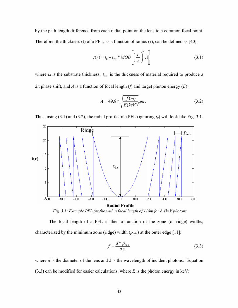
43
by the path length difference from each radial point on the lens to a common focal point.
Therefore, the thickness (t) of a PFL, as a function of radius (r), can be defined as [40]:
2
0 2( ) * ,1rt r t t MODAπ
= +
(3.1)
where t0 is the substrate thickness, π2t is the thickness of material required to produce a
2π phase shift, and A is a function of focal length (f) and target photon energy (E):
mkeVEmfA µ
)()(*8.49= . (3.2)
Thus, using (3.1) and (3.2), the radial profile of a PFL (ignoring t0) will look like Fig. 3.1.
The focal length of a PFL is then a function of the zone (or ridge) widths,
characterized by the minimum zone (ridge) width (pmin) at the outer edge [11]:
min*2
d pfλ
= (3.3)
where d is the diameter of the lens and λ is the wavelength of incident photons. Equation
(3.3) can be modified for easier calculations, where E is the photon energy in keV:
Radial Profile
t(r)
Pmin
t2π
Ridge
Fig. 3.1: Example PFL profile with a focal length of 118m for 8.4keV photons.
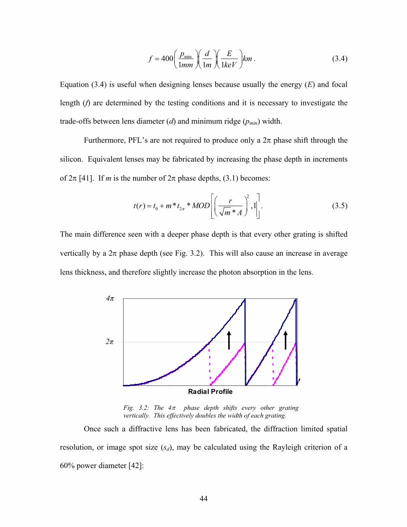
44
min4001 1 1p d Ef kmmm m keV
=
. (3.4)
Equation (3.4) is useful when designing lenses because usually the energy (E) and focal
length (f) are determined by the testing conditions and it is necessary to investigate the
trade-offs between lens diameter (d) and minimum ridge (pmin) width.
Furthermore, PFL’s are not required to produce only a 2π phase shift through the
silicon. Equivalent lenses may be fabricated by increasing the phase depth in increments
of 2π [41]. If m is the number of 2π phase depths, (3.1) becomes:
2
0 2( ) * * ,1*
rt r t m t MODm Aπ
= +
. (3.5)
The main difference seen with a deeper phase depth is that every other grating is shifted
vertically by a 2π phase depth (see Fig. 3.2). This will also cause an increase in average
lens thickness, and therefore slightly increase the photon absorption in the lens.
Once such a diffractive lens has been fabricated, the diffraction limited spatial
resolution, or image spot size (sd), may be calculated using the Rayleigh criterion of a
60% power diameter [42]:
Radial Profile
Fig. 3.2: The 4π phase depth shifts every other grating vertically. This effectively doubles the width of each grating.
2π
4π
45
1.22d
fsdλ
= . (3.6)
Although the spot size is of great importance when using Fresnel lenses in microscopy,
angular resolution (θd) is much more important in astronomy and will determine the
success of any tested PFL’s. The angular resolution can be calculated by:
fs
dd
d ==λθ 22.1 . (3.7)
3.3. PFL Mask Design Considerations
The success of gray-scale technology is dependent not only on the design of the
optical mask, but also on the quality of the pattern actually generated by the mask vendor.
As such, the cost of an optical mask will largely be a function of the feature dimensions
required. Since gray-scale technology relies on sub-resolution pixels in a projection
lithography system, the dimensions of the individual pixels on a mask will be quite small
(<3.0µm). As such, a large number of pixels are required to make a gray-scale structure,
which tends to increase the write time required by the mask fabrication tool, and that cost
is often relayed to the customer. Therefore, gray-scale optical masks will likely be more
expensive than other MEMS optical masks because of the high resolution and the long
write times required for the intricate patterns, a price you must pay to create a 3D
photoresist structure in one lithography step.
The following sections will describe the important factors to consider when
defining the pitch on the optical mask, as well as the constraints imposed on pixel design
by the mask vendor. These 2 factors together will limit the number of possible pixels. A
procedure is also outlined for selecting the appropriate pixels to be used in the design of a
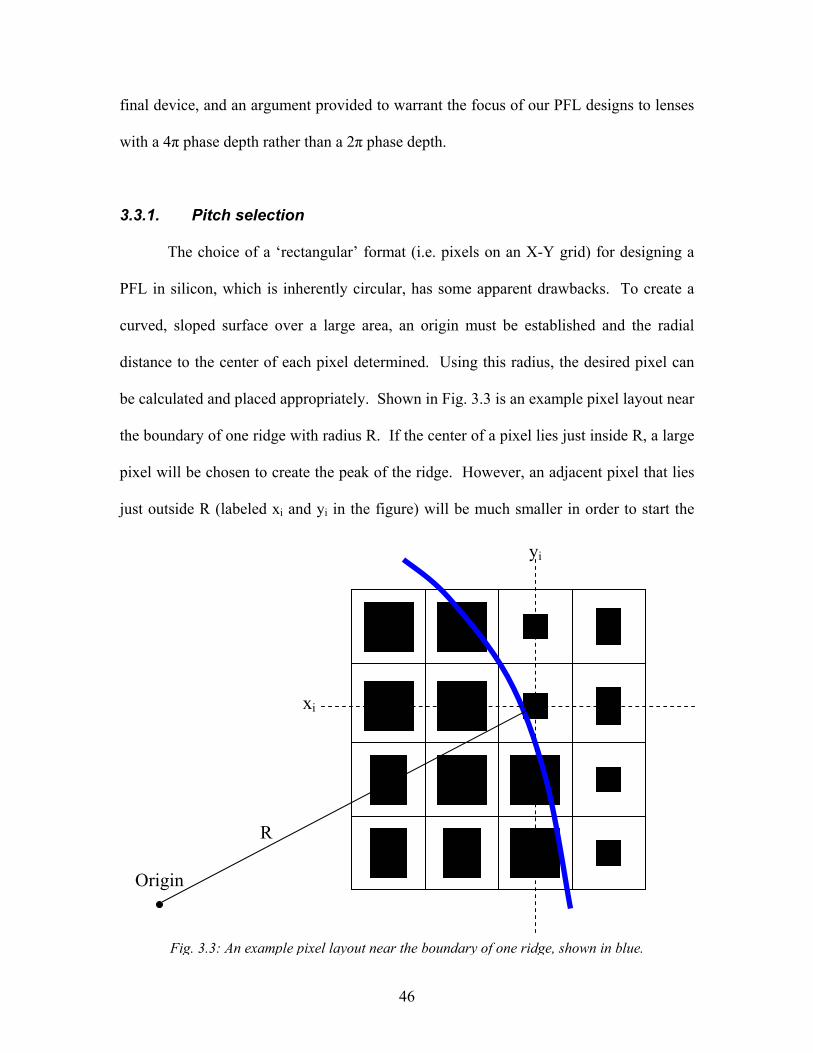
46
final device, and an argument provided to warrant the focus of our PFL designs to lenses
with a 4π phase depth rather than a 2π phase depth.
3.3.1. Pitch selection
The choice of a ‘rectangular’ format (i.e. pixels on an X-Y grid) for designing a
PFL in silicon, which is inherently circular, has some apparent drawbacks. To create a
curved, sloped surface over a large area, an origin must be established and the radial
distance to the center of each pixel determined. Using this radius, the desired pixel can
be calculated and placed appropriately. Shown in Fig. 3.3 is an example pixel layout near
the boundary of one ridge with radius R. If the center of a pixel lies just inside R, a large
pixel will be chosen to create the peak of the ridge. However, an adjacent pixel that lies
just outside R (labeled xi and yi in the figure) will be much smaller in order to start the
yi
Origin
xi
R
Fig. 3.3: An example pixel layout near the boundary of one ridge, shown in blue.
47
lower portion of the next ridge. This will cause some digital nature to our circular PFL’s
as the radius sweeps out a circle. The problem becomes analogous to making a circle on
a piece of graph paper by filling in boxes – the edges are never quite smooth, and the
accuracy of the circle depends on how large each box is (the pitch).
Thus, by selecting a pitch, the horizontal resolution of our pixel placement is
defined. A pitch of 2.8µm on the mask (the resolution limit determined in section 2.2.3),
means that after 5X reduction, the resolution of our PFL will be ~0.56µm. This
resolution is sufficient when making large features (>20µm wide), however as each ridge
is reduced in width, the number of pixels that can fit in that ridge decreases. Therefore,
control of the profile is reduced as fewer pixels are asked to do the work of many. The
obvious method of alleviating this problem is to reduce the chosen pitch to allow a larger
number of pixels to fit horizontally in the smaller ridges. However, as the pitch is
decreased, the number of pixels available within the constraints of the mask fabrication
will also decrease, possibly lowering PFL efficiency. Pixel constraints will be discussed
in detail in the following section.
A balance must be found between the horizontal resolution of gray-scale
structures in our PFL and the number of pixels available to produce the most accurate 3D
slope possible. While it should be possible to increase the number of available pixels by
using more accurate mask fabrication technologies, the cost of each optical mask would
increase and the gain in resolution would likely be small for the PFL’s being considered
here. Therefore, this research will use only the critical pitch (PC = 2.8µm on the optical
mask), resulting in an approximate resolution of ~0.56µm on the silicon PFL.
48
3.3.2. Pixel constraints
When comparing mask vendors, there are 2 main parameters of interest in gray-
scale lithography that will determine your pixel constraints: (1) minimum feature size
(Fm) and (2) electron beam spot size (S0). The minimum feature size is the smallest
feature dimension, opaque or clear, expected to be resolved on the mask after fabrication
(i.e. opaque boxes must have all dimensions larger than Fm and their edges cannot be
spaced closer than Fm). The spot size of the electron beam used to fabricate a mask is
important because it defines the smallest possible increment between subsequent pixel
sizes. Smaller spot sizes are advantageous because they can lead to larger pixel sets as
the permutations of pixel sizes can be increased while remaining within the Fm
constraints.
As described in Chapter 2 of this thesis, the method of gray-scale patterning
chosen to fabricate a PFL in silicon utilizes sub-resolution pixels located in an X-Y
format. Since optical masks are fabricated on systems that also use an X-Y format, it is
best to use rectangular pixels conforming to such a format to avoid pixilated
approximations of our pixels. Therefore, the dimensions of each rectangular pixel,
height(x) vs. length(y), must satisfy the following 3 identities derived from Fig. 3.4:
mFYX ≥, (3.8)
( )mC FPYX −≤, (3.9)
+=+=
0
0
**
SmFYSnFX
m
m where 0
*2,...1,0,
SFP
mn mC −= (3.10)
where PC is the critical pitch, or resolution limit, discussed in chapter 2 of this thesis. The
limiting case of (3.8) will result in the largest transmission through the mask, while (3.9)
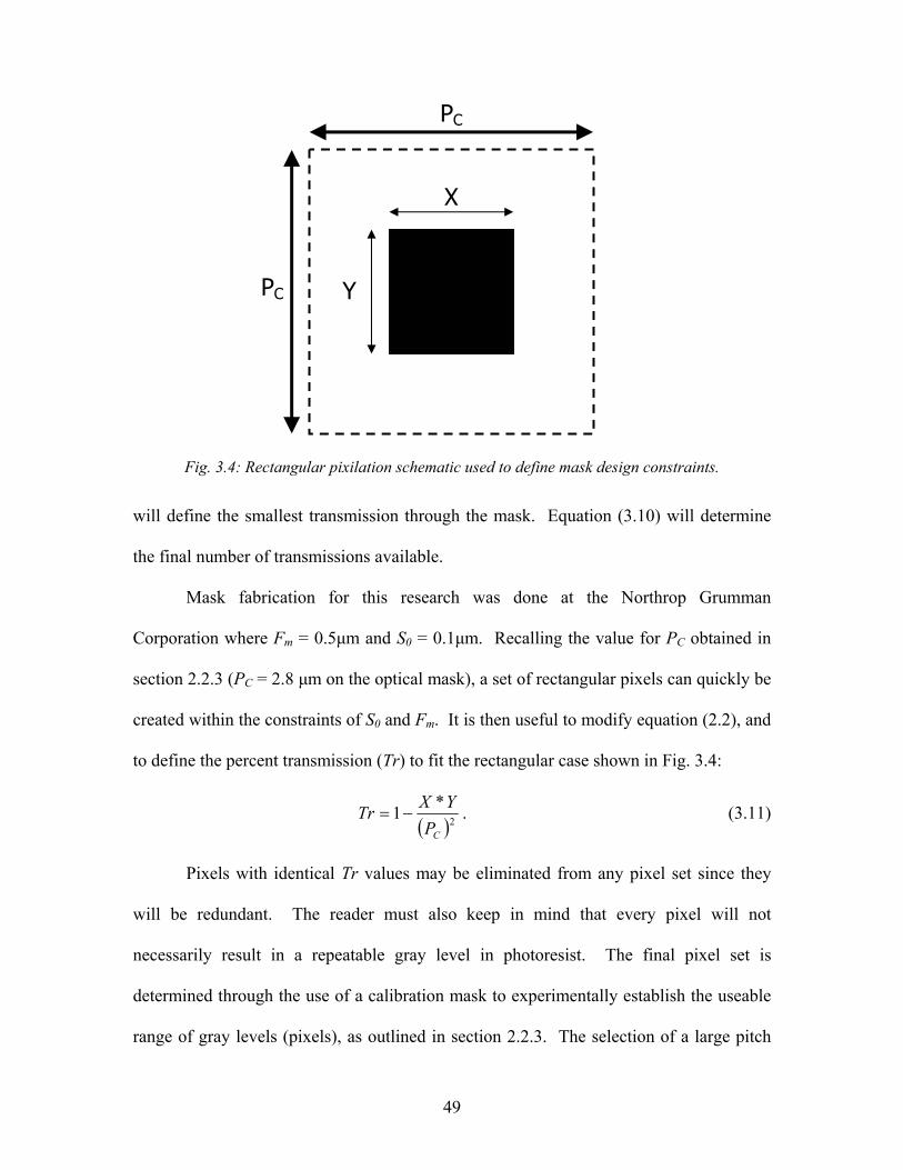
49
will define the smallest transmission through the mask. Equation (3.10) will determine
the final number of transmissions available.
Mask fabrication for this research was done at the Northrop Grumman
Corporation where Fm = 0.5µm and S0 = 0.1µm. Recalling the value for PC obtained in
section 2.2.3 (PC = 2.8 µm on the optical mask), a set of rectangular pixels can quickly be
created within the constraints of S0 and Fm. It is then useful to modify equation (2.2), and
to define the percent transmission (Tr) to fit the rectangular case shown in Fig. 3.4:
( )2
*1CP
YXTr −= . (3.11)
Pixels with identical Tr values may be eliminated from any pixel set since they
will be redundant. The reader must also keep in mind that every pixel will not
necessarily result in a repeatable gray level in photoresist. The final pixel set is
determined through the use of a calibration mask to experimentally establish the useable
range of gray levels (pixels), as outlined in section 2.2.3. The selection of a large pitch
PC
X
Y PC
Fig. 3.4: Rectangular pixilation schematic used to define mask design constraints.
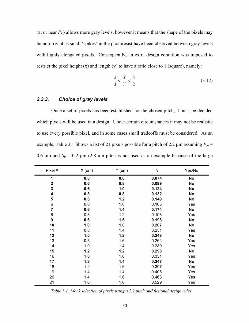
50
(at or near PC) allows more gray levels, however it means that the shape of the pixels may
be non-trivial as small ‘spikes’ in the photoresist have been observed between gray levels
with highly elongated pixels. Consequently, an extra design condition was imposed to
restrict the pixel height (x) and length (y) to have a ratio close to 1 (square), namely:
23
32
<<YX (3.12)
3.3.3. Choice of gray levels
Once a set of pixels has been established for the chosen pitch, it must be decided
which pixels will be used in a design. Under certain circumstances it may not be realistic
to use every possible pixel, and in some cases small tradeoffs must be considered. As an
example, Table 3.1 Shows a list of 21 pixels possible for a pitch of 2.2 µm assuming Fm =
0.6 µm and S0 = 0.2 µm (2.8 µm pitch is not used as an example because of the large
Pixel # X (um) Y (um) Tr Yes/No
1 0.6 0.6 0.074 No 2 0.6 0.8 0.099 No 3 0.6 1.0 0.124 No 4 0.8 0.8 0.132 No 5 0.6 1.2 0.149 No 6 0.8 1.0 0.165 Yes 7 0.6 1.4 0.174 No 8 0.8 1.2 0.198 Yes 9 0.6 1.6 0.198 No 10 1.0 1.0 0.207 No 11 0.8 1.4 0.231 Yes 12 1.0 1.2 0.248 No 13 0.8 1.6 0.264 Yes 14 1.0 1.4 0.289 Yes 15 1.2 1.2 0.298 No 16 1.0 1.6 0.331 Yes 17 1.2 1.4 0.347 No 18 1.2 1.6 0.397 Yes 19 1.4 1.4 0.405 Yes 20 1.4 1.6 0.463 Yes 21 1.6 1.6 0.529 Yes
Table 3.1: Mock selection of pixels using a 2.2 pitch and fictional design rules.
51
increase in rectangular permutations). A mock pixel selection procedure would go as
follows: It is important to eliminate pixels that will not be created consistently because
any loss of bottom gray levels will result in flat areas at the bottom of each ridge,
deforming the PFL profile and decreasing the efficiency. Supposing from the calibration
mask that Tr < 0.15 does not result in a useable gray level, pixels 1-5 are eliminated.
Pixels 8 and 9 result in the same Tr value and are therefore redundant, so pixel 9 is
eliminated. One can then compare the Tr values for the remaining pixels. If 2 successive
pixels are sufficiently close, it is unlikely that they will be consistently resolved in the
photoresist and one can usually be eliminated (the uncertainty during the rest of the gray-
scale process will be more of a determining factor). Using an arbitrary threshold of 0.02,
pixels 7, 10, 12, 15, and 17 are eliminated. The remaining 10 pixels can then be used to
produce any final structures.
Depending on the PFL dimensions, it may be beneficial to design for a smaller
number of well-defined levels rather than a larger number of less-uniform levels. In this
way, the levels could be more consistently defined and achieved. Additionally, the
pattern transfer may benefit from having a more step-like profile because of cycling the
passivation and etch steps during DRIE. If the profile becomes truly sloped, then the
passivation will no longer be on a ‘vertical’ sidewall where it is protected, and may be
prematurely removed, resulting in a loss of profile control.
The selection of a pixel set will obviously have an impact on the PFL design. If
only 10 pixels are possible, and therefore 10 gray levels, then the max efficiency using
equation (1.1) is 96.7%, which may or may not be sufficient depending on the other
design parameters of the lens. However, the number of gray levels available becomes
52
increasingly important if a deeper phase depth is used, since twice as many gray levels
will be necessary to maintain a similar efficiency. As a minimum, 8 or more levels per
phase depth should be available in our PFL designs in order to target efficiencies at or
above 90%.
3.3.4. Multiple Phase depths
As stated earlier in section 3.2, equivalent PFL’s may be constructed by
increasing the phase depth from 2π to 4π or more, with the penalty being an increase in
absorption. Since silicon PFL’s are being considered here, the increase in absorption for
a 4π lens, especially as the energy is increased, is tolerable. Instead of an average
thickness of t2π/2, there will be an average thickness of t2π over the entire lens. For
8.4keV photons with a photon attenuation length of 80µm in silicon, the intrinsic
absorption in the lens increases from 13% for a 2π phase depth to 23% for a 4π phase
depth. The intrinsic absorption will be smaller for higher energy lenses.
Designs using multiple phase depths for this PFL are specifically investigated
because of the nature of gray-scale technology and the peculiar dimensions required. By
increasing the phase depth from 2π to 4π, the width of each ridge in photoresist is
effectively doubled. Since gray-scale technology can easily deliver 30+ gray levels using
PC, more than 16 gray levels per phase depth are still possible. One advantage of
doubling the width of each ridge in photoresist is that the lithography processing is more
readily achieved because the aspect ratio of the photoresist structures is reduced.
A second important aspect of increasing the phase depth is that the etch depth
required in DRIE is doubled, which will assist in the pattern transfer. Consider an
53
8.4keV PFL. The t2π phase depth using (1.2) is 21.4µm in silicon, which can be easily
achieved in silicon using DRIE. Since the lithography processing is more consistent with
thicker photoresist and thicker gray levels, an entire gray-scale pattern is commonly
~3µm thick. Such a pattern would then require a selectivity of 7:1 to transfer it entirely,
which is extremely low (see section 2.3.2). By increasing the target phase depth to 4π
and doubling the number of gray levels, the target depth is now 42.8µm and the
selectivity can be increased to 14:1. This etch selectivity is still very low for DRIE, but is
much more reasonable. Specific steps taken to address this issue will be discussed in
Chapter 4 of this thesis. Increasing the phase depth beyond 4π for an 8.4keV lens will
further increase the absorption and require a larger number of gray levels. Therefore,
8.4keV PFL’s with 4π phase depths were chosen as the focus of this research.
3.4. Gaussian Approximation Method
To create silicon PFL’s with high efficiency, every pixel in the optical mask
design must be individually placed. Previously, rectangular gray levels were created in
this research by placing a single pixel and repeating it in an array. For small geometries
with few gray levels, a structure design could be done entirely by hand with only a small
knowledge of previous experiments. However, for millimeter sized PFL’s, each gray
level will be curved and as such each pixel must be placed individually. With >106 pixels
required to make each test lens, an automated system is necessary to create the
appropriate pixel at every point. The Gaussian approximation method presented in the
next sections will outline the method by which an optimum pixel may be selected for
each pixel location to accurately re-create any desired profile, including but not limited
to, the PFL profile defined in equation (3.5). Alternate gray-scale photoresist
54
linearization schemes have been investigated [43]. Linear gratings with 8 levels were
fabricated, however the authors did not demonstrate arbitrary profiles, nor did the model
facilitate integration into complicated structure designs. The authors also used High-
Energy-Beam-Sensitive (HEBS) glass in contact lithography rather than the pixilated
approach with projection lithography that was selected for this research.
3.4.1. Experiment
The Gaussian approximation relies on the calibration mask of section 2.2.3 and
the standard lithography process defined in section 2.2.4. First, the standard gray-scale
lithography process is performed using the calibration mask. Each wedge designed on
the calibration mask has an opaque photoresist block at one end as a reference point, with
adjacent large square gray levels made with pixels of descending size. The photoresist
height of each level is associated with a particular pixel by counting the steps from the
opaque square. Thus, for a given photoresist wedge produced by the calibration mask,
the Tr value can be calculated and related to the final photoresist height. Table 3.2 shows
some example data taken from structures with a pitch of 2.8µm. The Tr value, from the
Normalized Height in Photoresist, Hp (µm) Square Pixel Size (µm) Tr
Sample 1 Sample 2 Sample 3 Sample 4 2.1 0.438 0.39 0.42 0.42 0.42 2.0 0.490 0.30 0.33 0.32 0.32 1.9 0.540 0.23 0.24 0.25 0.25 1.8 0.587 0.18 0.19 0.19 0.19 1.7 0.631 0.12 0.14 0.14 0.14 1.6 0.673 0.09 0.09 0.10 0.10 1.5 0.713 0.05 0.05 0.06 0.07
Table 3.2: Gray level height data taken from a structures using a 2.8µm pitch.
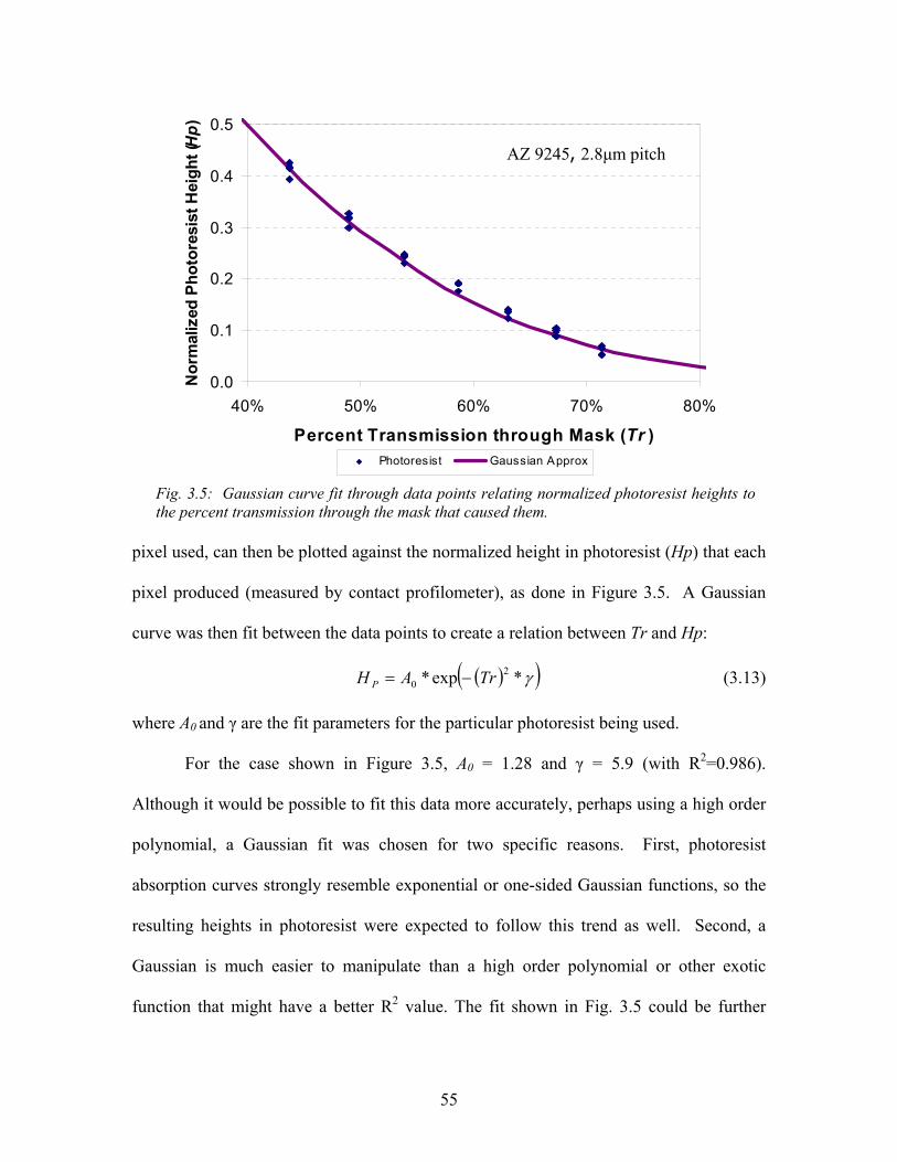
55
pixel used, can then be plotted against the normalized height in photoresist (Hp) that each
pixel produced (measured by contact profilometer), as done in Figure 3.5. A Gaussian
curve was then fit between the data points to create a relation between Tr and Hp:
( )( )γ*exp* 20 TrAH P −= (3.13)
where A0 and γ are the fit parameters for the particular photoresist being used.
For the case shown in Figure 3.5, A0 = 1.28 and γ = 5.9 (with R2=0.986).
Although it would be possible to fit this data more accurately, perhaps using a high order
polynomial, a Gaussian fit was chosen for two specific reasons. First, photoresist
absorption curves strongly resemble exponential or one-sided Gaussian functions, so the
resulting heights in photoresist were expected to follow this trend as well. Second, a
Gaussian is much easier to manipulate than a high order polynomial or other exotic
function that might have a better R2 value. The fit shown in Fig. 3.5 could be further
0.0
0.1
0.2
0.3
0.4
0.5
40% 50% 60% 70% 80%
Percent Transmission through Mask (Tr )
Nor
mal
ized
Pho
tore
sist
Hei
ght (
Hp)
Photoresist Gaussian Approx
AZ 9245, 2.8µm pitch
Fig. 3.5: Gaussian curve fit through data points relating normalized photoresist heights to the percent transmission through the mask that caused them.
56
optimized by either incorporating small offsets in x or y, or possibly using a slightly
simpler exponential form:
( )γ*exp*0 TrAH P −= (3.14)
As is evident in Figure 3.4, the Gaussian approximation provides a reasonably
good fit for the data in question for initial PFL iterations, and as such will be extended as
the method of choice throughout this analysis.
Once suitable fit parameters have been determined, the true power of the
Gaussian approximation is realized as the equation is reversed:
γ
−
= 0
lnAH
Tr
P
. (3.15)
In equation (3.15), we now have a case where Tr is only a function of Hp, the normalized
height in photoresist. Therefore, equation (3.15) has the ability to calculate the optimum
Tr value necessary to produce a desired Hp. Naturally the desired Hp is simply a
normalized version of equation (3.5), meaning that the optimum Tr value is now simply a
function of the radius. By combining equations (3.15) and (3.11), the pixel size can be
directly related to the desired Hp at each radial point:
( )
−
−==γ
02
ln1**
AH
PYXA
P
Cpixel . (3.16)
By using the Gaussian approximation method described above, much of the
modeling and theory behind the gray-scale lithography process may be abbreviated. This
approximation is especially helpful since the gray-scale process is so heavily dependent
57
upon process conditions that are difficult to model from one lab to the next. Additionally,
creating a custom Gaussian approximation for a new lab can be carried out
simultaneously as a standardized lithography process is developed with the calibration
mask, as would be done for traditional lithography anyway. Therefore, with the addition
of only a few profilometer measurements and one curve fit, gray-scale masks may be
designed to precisely mimic any desired slope.
3.4.2. Integration into C Program Design
As stated earlier, the individual placement of each pixel may not be realistically
done by hand. By incorporating equation (3.16) into a program developed using the C++
programming language, all pixels may be automatically determined with ease and read
into a CAD layout tool with scripting capabilities (Tanner’s L-edit). (Throughout the
following analysis, it is assumed that a pixel set has already been established.)
Additionally, by symmetry, a circle defined on an X-Y grid can be created by defining
only the 1st quadrant, and then using the CAD tool to mirror and/or rotate 3 more 90°
wedges. Thus only the pixels necessary to make ¼ of a PFL must be individually defined
(or 1/8 of a PFL with 7 more identical wedges).
Assuming the desired focal length, photon energy, phase depth, and radius (R) on
the wafer have been defined by the user, a C program can simply walk through and
address every point on the mask’s X-Y grid from the origin (0,0) to the boundary of the
lens (5R, 5R) (assuming a 5X reduction by the projection lithography system will result
in a PFL of radius R). By incrementing x and y by PC on the optical mask, every pixel
location in x and y on the interval 0 to 5R will be individually addressed. Since PFL
58
equation (3.5) is defined by the radial distance from the origin, the program will
transform each xA and yB coordinates into a radial coordinate, rAB:
22
55
+
= BA
AByxr . (3.17)
To find the desired Hp at rAB, the part of equation (3.5) that is radially dependent
is normalized to the highest expected Hp (Hpmax) of the pixel set being used:
== 1,
**)(
2
max Amr
MODHprtHp ABAB . (3.18)
Plugging equation (3.18) into (3.16), the optimum pixel size required to produce such a
height in photoresist is obtained. Since the optimum pixel size will probably not exist,
the optimum value can be compared to the available pixels and rounded to the closest
pixel. It is through this final rounding procedure that the stair-step nature of our PFL
comes about, as each point on the curve is rounded to the nearest available step.
As a quick aside, this rounding effect may influence the desired pixel set. As the
size of each pixel increases, the difference in area between pixel permutations become
farther and farther apart. This gap in area creates large gaps between Tr values which
will cause the profile to look rather poor as the steps towards the top of a device become
much larger than the steps at the bottom of a device. Such a non-uniform step
approximation to the desired profile, which was highlighted by the Gaussian
approximation, will decrease the efficiency of any PFLs created in this manor.
Consequently, it may be appropriate to truncate the pixel set before using all possible
pixels in order to maintain evenly spaced gray levels.
59
Once the best pixel has been selected for a particular point, the program outputs a
set of commands into a text file specifying the location and size of a box to be created by
the CAD layout tool. Once all locations have been addressed, the final text file may be
imported into the CAD layout tool using command line scripting. Since the number of
pixels is often very large (>106), the final text file may take as long as 1-2 days to import
an entire design into a layout file (Dell PC with 1.8GHz Pentium 4 processor and 512MB
RAM), creating files as large as 500MB. Such large files make data storage and
manipulation tedious while finalizing the rest of the mask design, and any changes that
require re-creating the design will come with an enormous time penalty. This penalty can
be alleviated somewhat by making multiple smaller command files to allow for some
design inspection, hopefully avoiding minor programming mistakes that could cost days
of computation time.
3.5. PFL Device Design Parameters
In addition to various test structures, three primary PFL designs were developed
and placed on two successive optical masks. Table 3.3 shows the properties of each of
these three lenses. Chronologically, lens A was the first full PFL to be fabricated in
silicon. Lenses B and C followed with more accurate Gaussian fit parameters and larger
diameters.
The combination of these three lenses will enable the investigation of multiple
aspects of PFL design and fabrication using gray-scale technology. To evaluate the
profile difference between fewer sharply defined gray levels and a larger number of
‘blended’ gray levels, lenses A and B have been designed with 32 levels, while lens C has
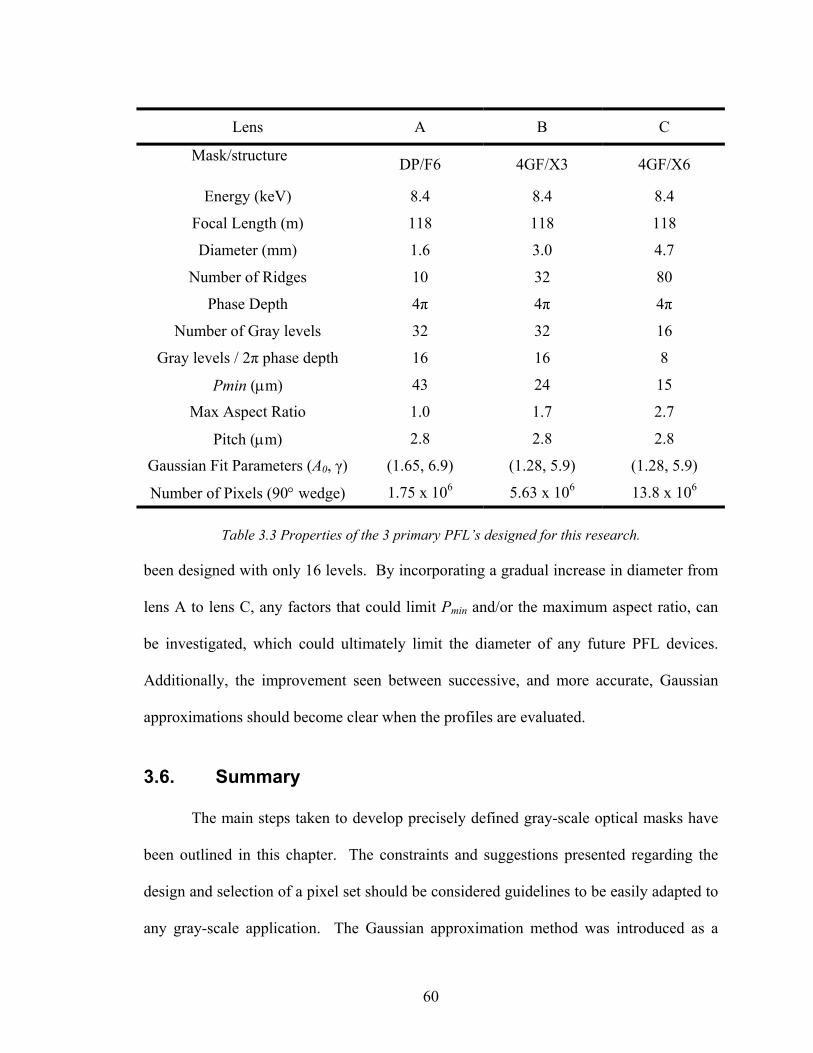
60
been designed with only 16 levels. By incorporating a gradual increase in diameter from
lens A to lens C, any factors that could limit Pmin and/or the maximum aspect ratio, can
be investigated, which could ultimately limit the diameter of any future PFL devices.
Additionally, the improvement seen between successive, and more accurate, Gaussian
approximations should become clear when the profiles are evaluated.
3.6. Summary
The main steps taken to develop precisely defined gray-scale optical masks have
been outlined in this chapter. The constraints and suggestions presented regarding the
design and selection of a pixel set should be considered guidelines to be easily adapted to
any gray-scale application. The Gaussian approximation method was introduced as a
Lens A B C
Mask/structure DP/F6 4GF/X3 4GF/X6
Energy (keV) 8.4 8.4 8.4
Focal Length (m) 118 118 118
Diameter (mm) 1.6 3.0 4.7
Number of Ridges 10 32 80
Phase Depth 4π 4π 4π
Number of Gray levels 32 32 16
Gray levels / 2π phase depth 16 16 8
Pmin (µm) 43 24 15
Max Aspect Ratio 1.0 1.7 2.7
Pitch (µm) 2.8 2.8 2.8
Gaussian Fit Parameters (A0, γ) (1.65, 6.9) (1.28, 5.9) (1.28, 5.9)
Number of Pixels (90° wedge) 1.75 x 10⁶ 5.63 x 10⁶ 13.8 x 10⁶
Table 3.3 Properties of the 3 primary PFL’s designed for this research.
61
method of precisely placing many appropriate pixels to create a desired height profile in
photoresist, in our case re-creating the PFL equations given in section 3.2. A method of
integrating pixel design limitations and the Gaussian approximation into a custom C
program was outlined and used to develop multiple gray-scale optical masks containing
three different PFL designs. The success and accuracy of the design methodologies
presented herein will be assessed in Chapter 4 of this thesis as the fabrication aspects of
developing a PFL in silicon are discussed and their profiles evaluated.
62
4. Lens Fabrication 4.1. Introduction
As discussed in the previous chapter, a large amount of work goes into the design
of each gray-scale structure created. However, a wide understanding of the fabrication
challenges involved is necessary when attempting to produce an accurate structure in the
silicon, largely because the mask design is dependent on consistent lithography
processing and precise control of etching characteristics. The typical process flow for a
PFL wafer starts with the lithography, then the photoresist height is measured to
determine the appropriate etch selectivity, and the wafer is subsequently etched in DRIE
with the best available etch recipe. For the results presented in this chapter, all
lithography processing was carried out by C. Mike Waits at the Laboratory for Physical
Sciences (LPS) in College Park, MD, while I performed all dry etching at the U.S. Army
Research Laboratory (ARL) in Adelphi, MD. Analysis tools used to evaluate and image
various results were located at ARL or on the campus of the University of Maryland.
This chapter will address all aspects of this research regarding the fabrication of a
PFL in silicon. Lithography results will be discussed in detail for ridge widths ranging
from hundreds of micrometers down to a few micrometers. Examples will be given that
show the impact of using a pixilated design for fabricating PFL’s in photoresist, with
comments on how these results will limit future designs. Contact and optical
profilometer measurements of photoresist profiles will confirm that the methodologies
employed for designing our PFL masks, namely the Gaussian approximation and pixel
design methods outlined in Chapter 3, accurately mimic the desired PFL profile. Key
63
issues regarding the DRIE transfer of a photoresist PFL will be discussed, and a
modification to the standard Bosch process will be introduced as a means of lowering
etch selectivity to the desired range. Etch results obtained using this low selectivity
process will be presented and the method by which metrology is performed on a silicon
PFL profile will also be discussed. Two problems will be analyzed with respect to their
possible impact on lens performance: aspect ratio dependent etching (ARDE) and surface
roughness. Finally, a method will be introduced to calculate the approximate efficiency
of a silicon PFL profile without testing the lens in an X-ray beam line. This method will
be used to compare the different silicon PFL profiles designed and fabricated.
4.2. Lithography Results
All lithography results in this chapter were achieved using the standard
lithography process developed in Chapter 2 of this thesis. The following sections will
present and comment on multiple photoresist PFL structures that have been fabricated
using gray-scale lithography. First, lithography results will confirm the digital behavior
of the circular approximations made when designing our PFL structures (discussed in
Chapter 3). The limiting cases of this digital behavior will be presented. The metrology
method used to investigate the photoresist profiles will be discussed as it is an important
aspect of evaluating each photoresist profile. Ultimately, these metrology measurements
will be used to confirm the accuracy of the mask design method developed in Chapter 3.
4.2.1. Photoresist PFL Structures
A number of photoresist PFL’s and test structures have been fabricated during this
research, yet only a small sampling will be presented in this thesis in order to highlight
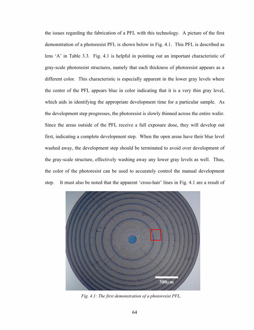
64
the issues regarding the fabrication of a PFL with this technology. A picture of the first
demonstration of a photoresist PFL is shown below in Fig. 4.1. This PFL is described as
lens ‘A’ in Table 3.3. Fig. 4.1 is helpful in pointing out an important characteristic of
gray-scale photoresist structures, namely that each thickness of photoresist appears as a
different color. This characteristic is especially apparent in the lower gray levels where
the center of the PFL appears blue in color indicating that it is a very thin gray level,
which aids in identifying the appropriate development time for a particular sample. As
the development step progresses, the photoresist is slowly thinned across the entire wafer.
Since the areas outside of the PFL receive a full exposure dose, they will develop out
first, indicating a complete development step. When the open areas have their blue level
washed away, the development step should be terminated to avoid over development of
the gray-scale structure, effectively washing away any lower gray levels as well. Thus,
the color of the photoresist can be used to accurately control the manual development
step. It must also be noted that the apparent ‘cross-hair’ lines in Fig. 4.1 are a result of
Fig. 4.1: The first demonstration of a photoresist PFL.
300µm
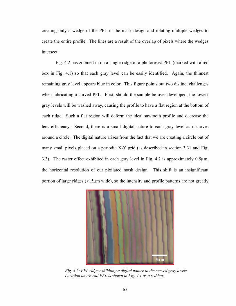
65
creating only a wedge of the PFL in the mask design and rotating multiple wedges to
create the entire profile. The lines are a result of the overlap of pixels where the wedges
intersect.
Fig. 4.2 has zoomed in on a single ridge of a photoresist PFL (marked with a red
box in Fig. 4.1) so that each gray level can be easily identified. Again, the thinnest
remaining gray level appears blue in color. This figure points out two distinct challenges
when fabricating a curved PFL. First, should the sample be over-developed, the lowest
gray levels will be washed away, causing the profile to have a flat region at the bottom of
each ridge. Such a flat region will deform the ideal sawtooth profile and decrease the
lens efficiency. Second, there is a small digital nature to each gray level as it curves
around a circle. The digital nature arises from the fact that we are creating a circle out of
many small pixels placed on a periodic X-Y grid (as described in section 3.31 and Fig.
3.3). The raster effect exhibited in each gray level in Fig. 4.2 is approximately 0.5µm,
the horizontal resolution of our pixilated mask design. This shift is an insignificant
portion of large ridges (>15µm wide), so the intensity and profile patterns are not greatly
5µm
Fig. 4.2: PFL ridge exhibiting a digital nature to the curved gray levels. Location on overall PFL is shown in Fig. 4.1 as a red box.
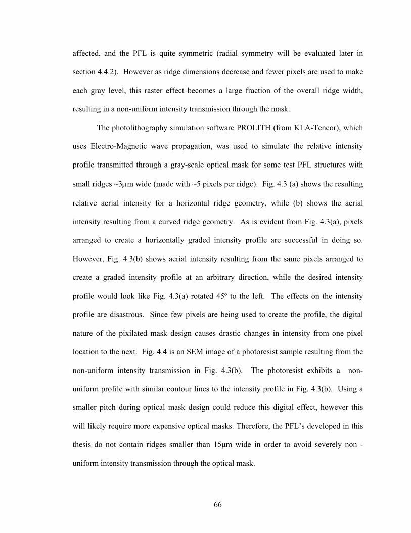
66
affected, and the PFL is quite symmetric (radial symmetry will be evaluated later in
section 4.4.2). However as ridge dimensions decrease and fewer pixels are used to make
each gray level, this raster effect becomes a large fraction of the overall ridge width,
resulting in a non-uniform intensity transmission through the mask.
The photolithography simulation software PROLITH (from KLA-Tencor), which
uses Electro-Magnetic wave propagation, was used to simulate the relative intensity
profile transmitted through a gray-scale optical mask for some test PFL structures with
small ridges ~3µm wide (made with ~5 pixels per ridge). Fig. 4.3 (a) shows the resulting
relative aerial intensity for a horizontal ridge geometry, while (b) shows the aerial
intensity resulting from a curved ridge geometry. As is evident from Fig. 4.3(a), pixels
arranged to create a horizontally graded intensity profile are successful in doing so.
However, Fig. 4.3(b) shows aerial intensity resulting from the same pixels arranged to
create a graded intensity profile at an arbitrary direction, while the desired intensity
profile would look like Fig. 4.3(a) rotated 45º to the left. The effects on the intensity
profile are disastrous. Since few pixels are being used to create the profile, the digital
nature of the pixilated mask design causes drastic changes in intensity from one pixel
location to the next. Fig. 4.4 is an SEM image of a photoresist sample resulting from the
non-uniform intensity transmission in Fig. 4.3(b). The photoresist exhibits a non-
uniform profile with similar contour lines to the intensity profile in Fig. 4.3(b). Using a
smaller pitch during optical mask design could reduce this digital effect, however this
will likely require more expensive optical masks. Therefore, the PFL’s developed in this
thesis do not contain ridges smaller than 15µm wide in order to avoid severely non -
uniform intensity transmission through the optical mask.
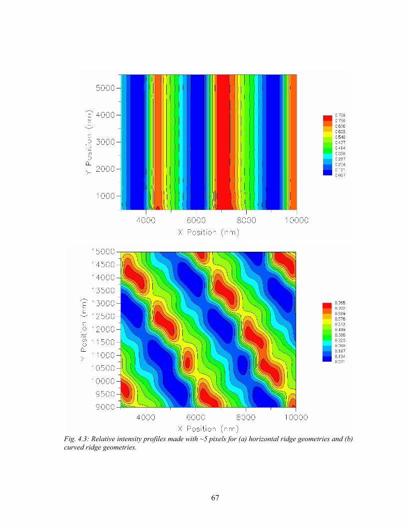
67
Fig. 4.3: Relative intensity profiles made with ~5 pixels for (a) horizontal ridge geometries and (b) curved ridge geometries.
68
4.2.2. PFL Metrology (Photoresist)
We have shown that photoresist PFL structures have been fabricated using gray-
scale lithography, however the goal of this research is to produce structures with specific
profiles, and therefore we must investigate exactly what profile has been fabricated in the
photoresist. Metrology measurements of photoresist are often done with a contact
profilometer, which physically drags a stylus tip across a photoresist sample in order to
measure the profile. Provided the contact force is low, this method generally will not
scratch or deform your photoresist. Another option for measuring our photoresist
profiles is to use an optical profilometer, which measures light reflected from the surface.
Since photoresist is semi-transparent, samples measured by optical profilometry were
coated with a 20nm layer of Au. Each measurement method has advantages and will be
used for separate purposes described below.
Fig. 4.4: SEM image of small curved ridges in photoresist resulting from the non-uniform intensity transmission exhibited in Fig. 4.3(b).
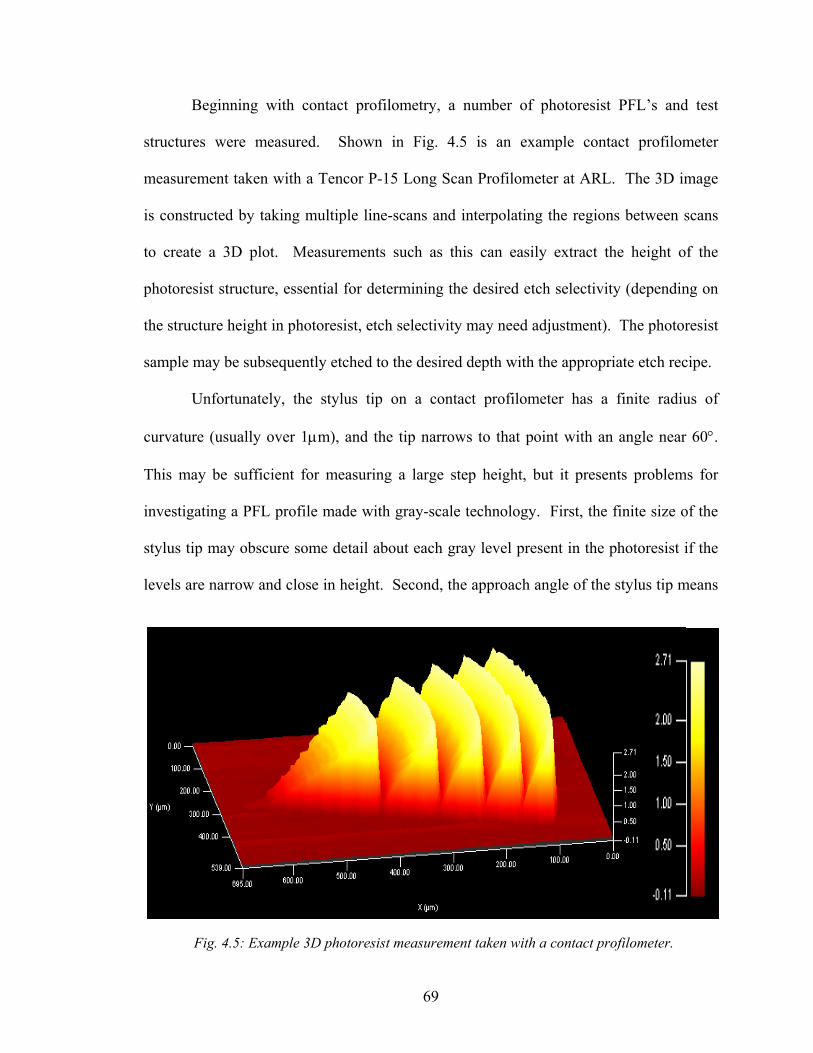
69
Beginning with contact profilometry, a number of photoresist PFL’s and test
structures were measured. Shown in Fig. 4.5 is an example contact profilometer
measurement taken with a Tencor P-15 Long Scan Profilometer at ARL. The 3D image
is constructed by taking multiple line-scans and interpolating the regions between scans
to create a 3D plot. Measurements such as this can easily extract the height of the
photoresist structure, essential for determining the desired etch selectivity (depending on
the structure height in photoresist, etch selectivity may need adjustment). The photoresist
sample may be subsequently etched to the desired depth with the appropriate etch recipe.
Unfortunately, the stylus tip on a contact profilometer has a finite radius of
curvature (usually over 1µm), and the tip narrows to that point with an angle near 60°.
This may be sufficient for measuring a large step height, but it presents problems for
investigating a PFL profile made with gray-scale technology. First, the finite size of the
stylus tip may obscure some detail about each gray level present in the photoresist if the
levels are narrow and close in height. Second, the approach angle of the stylus tip means
Fig. 4.5: Example 3D photoresist measurement taken with a contact profilometer.
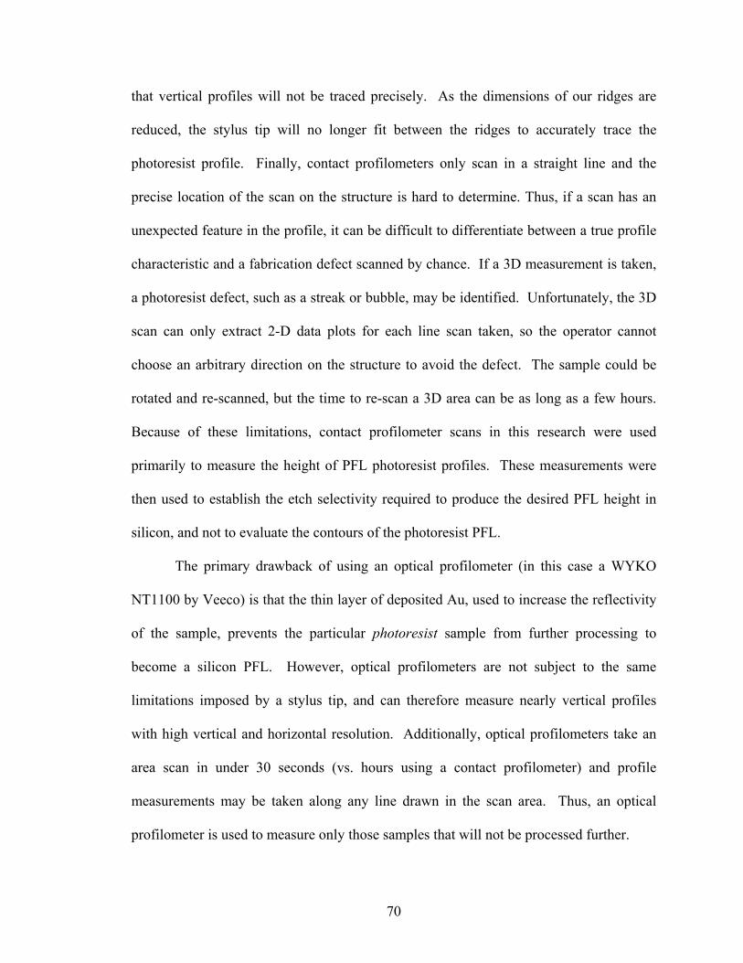
70
that vertical profiles will not be traced precisely. As the dimensions of our ridges are
reduced, the stylus tip will no longer fit between the ridges to accurately trace the
photoresist profile. Finally, contact profilometers only scan in a straight line and the
precise location of the scan on the structure is hard to determine. Thus, if a scan has an
unexpected feature in the profile, it can be difficult to differentiate between a true profile
characteristic and a fabrication defect scanned by chance. If a 3D measurement is taken,
a photoresist defect, such as a streak or bubble, may be identified. Unfortunately, the 3D
scan can only extract 2-D data plots for each line scan taken, so the operator cannot
choose an arbitrary direction on the structure to avoid the defect. The sample could be
rotated and re-scanned, but the time to re-scan a 3D area can be as long as a few hours.
Because of these limitations, contact profilometer scans in this research were used
primarily to measure the height of PFL photoresist profiles. These measurements were
then used to establish the etch selectivity required to produce the desired PFL height in
silicon, and not to evaluate the contours of the photoresist PFL.
The primary drawback of using an optical profilometer (in this case a WYKO
NT1100 by Veeco) is that the thin layer of deposited Au, used to increase the reflectivity
of the sample, prevents the particular photoresist sample from further processing to
become a silicon PFL. However, optical profilometers are not subject to the same
limitations imposed by a stylus tip, and can therefore measure nearly vertical profiles
with high vertical and horizontal resolution. Additionally, optical profilometers take an
area scan in under 30 seconds (vs. hours using a contact profilometer) and profile
measurements may be taken along any line drawn in the scan area. Thus, an optical
profilometer is used to measure only those samples that will not be processed further.
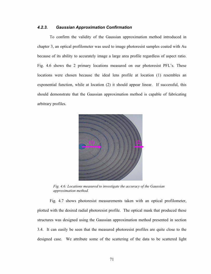
71
4.2.3. Gaussian Approximation Confirmation
To confirm the validity of the Gaussian approximation method introduced in
chapter 3, an optical profilometer was used to image photoresist samples coated with Au
because of its ability to accurately image a large area profile regardless of aspect ratio.
Fig. 4.6 shows the 2 primary locations measured on our photoresist PFL’s. These
locations were chosen because the ideal lens profile at location (1) resembles an
exponential function, while at location (2) it should appear linear. If successful, this
should demonstrate that the Gaussian approximation method is capable of fabricating
arbitrary profiles.
Fig. 4.7 shows photoresist measurements taken with an optical profilometer,
plotted with the desired radial photoresist profile. The optical mask that produced these
structures was designed using the Gaussian approximation method presented in section
3.4. It can easily be seen that the measured photoresist profiles are quite close to the
designed case. We attribute some of the scattering of the data to be scattered light
Fig. 4.6: Locations measured to investigate the accuracy of the Gaussian approximation method.
(1) (2)
72
reflecting from the thin Au coating and the photoresist surface roughness. The strong
resemblance between the fabricated photoresist PFL profiles and the desired profiles
confirms that the Gaussian approximation method introduced in this thesis is a valid and
useful tool for precisely designing 3D structures using gray-scale technology.
4.3. Dry Etching Results
The importance of accurately transferring a 3D photoresist gray-scale structure
was underscored in section 2.3.2 as the vertical dimensions of a silicon gray-scale
First Ridge
0
0.5
1
1.5
2
2.5
3
0 50 100 150 200 250 300
Radius (um)
Hei
ght (
um)
Designed PhotoresistFinal 2 Ridges
0
0.5
1
1.5
2
2.5
3
735 755 775 795 815
Radius (um)
Hei
ght (
um)
Designed Photoresist
Fig. 4.7: PFL photoresist profiles fabricated using the Gaussian approximation method closely mimic the desired profile.
73
structure will be dependent on the etch selectivity during DRIE. An initial investigation
regarding the control of etch selectivity during DRIE was presented in section 2.3.3.
Since the PFL photoresist patterns described in the preceding sections are routinely ~3µm
thick, and given the target 4π phase depth of 43µm, a controlled DRIE etch selectivity of
~14:1 will be necessary to achieve the appropriate vertical dimensions in silicon (each
wafer will be measured individually before etching to allow any necessary final tuning of
etch selectivity).
The following sections will discuss the results achieved using traditional etch
recipes like those presented in section 2.3.3, and also results achieved using a novel
modified Bosch process with an Oxygen-only step. Analysis will then be provided
regarding the aspect ratio dependent etching (ARDE) characteristics of the successful
etch recipes, and the expected impact of surface roughness on PFL performance.
4.3.1. General DRIE Results
During the etch selectivity characterization of section 2.3.3, a number of test PFL
structures were successfully transferred into the silicon. However, each etch selectivity
in that characterization was much higher than desired, producing adverse results. An
example of a transferred structure is shown below in Fig. 4.8. This 90° PFL wedge was
etched using a recipe with an etch selectivity of 70:1. After etching to a depth of 100µm
in the silicon, the entire gray-scale photoresist pattern still has not fully transferred, when
ideally the entire pattern needs to be transferred in less than half this depth. It is also easy
to see in Fig. 4.8 that some gray levels appear uneven, and this non-uniformity is
attributed to the photoresist structures and not the etch process. Fig. 4.8 shows the first
successful transfer of a curved PFL test structure into the silicon.
74
4.3.2. DRIE with Oxygen-only step
For the successful fabrication of the silicon PFL’s being considered in this
research, a recipe with extremely low etch selectivity is imperative. By referring back to
section 2.3.1 where DRIE is described, recall that etch selectivity is simply a ratio of etch
rates, namely the silicon etch rate divided by the photoresist etch rate. Therefore, to
achieve low etch selectivity, the photoresist etch rate must be increased without a large
effect on the silicon etch rate. In order to accomplish such a goal, I will introduce the
concept of a modified Bosch process with an Oxygen-only step.
One process that is widely used in MEMS and the IC industry, is an Oxygen (O2)
plasma to remove residual photoresist films after lithography. Such a process is
advantageous in MEMS because the O2 plasma removes most organic materials quickly,
like photoresist, without affecting underlying materials such as silicon or silicon-dioxide.
This fact works to my advantage for two reasons: First, most dry etch tools have O2
plumbing already available because it is commonly used for surface or chamber cleaning.
So no additional modifications to the DRIE system are required. Second, the O2 plasma
Fig. 4.8: Initial pattern transfer of a 90° PFL wedge with a high selectivity.
75
should only attack the photoresist layer, and not the underlying silicon, increasing only
the photoresist etch rate.
I have chosen to integrate an Oxygen-only etch step into the standard Bosch
process to increase the photoresist etch rate without increasing the silicon etch rate, thus
creating a novel modified Bosch process with low selectivity. Table 4.1 shows an etch
recipe with an original selectivity of 70:1 that now incorporates an Oxygen-only step.
The additional Oxygen-only step also contains a small flow of Ar to help maintain a
steady and uniform plasma. The other gasses, C4F8 and SF6, were not included in the
new step to minimize their chemical reactions with the O2, thus keeping the steps as
separated as possible.
The goal behind modifying the Bosch process with a short Oxygen-only etch step
is to remove a thin layer of photoresist from the top of the 3D photoresist pattern after
each passivation and etch step, to increase the overall photoresist etch rate. An
exaggeration of this process is shown in Fig. 4.9. Fig. 4.9(a) shows an initial photoresist
3D structure, while Fig. 4.9(b) shows this structure after the first etch step has been
completed with a high etch selectivity, leaving the photoresist virtually unchanged. The
subsequent Oxygen-only step, shown in Fig. 4.9(c), removes a thin layer of photoresist
before moving on to the passivation step of the following cycle, shown in Fig. 4.9(d). By
Step Ar (sccm)
C4F8 (sccm)
SF6 (sccm)
O2 (sccm)
Pressure (mTorr)
Chamber Temp(°C)
Electrode Power (W)
Time (sec)
Passivation 40 70 0 0 19 20 1 5
Etch 40 0 100 0 19 20 10 8
Oxygen-step 40 0 0 70 19 20 8 0-6
Table 4.1: Modified Bosch process using an Oxygen-only step.
76
modulating the length of the Oxygen-only plasma step, the amount of photoresist
removed during each cycle may be changed dramatically, therefore reducing the etch
selectivity.
The primary advantage of changing the etch selectivity in this manor is that it can
be tuned over a wide range (with minimal effect on sidewall profile since the main etch
steps that determine sidewall profile remain unchanged). Table 4.2 shows data taken
from 4 samples etched with various lengths of an Oxygen-only step. The etch selectivity
was successfully modulated from 70:1 down to 14:1 by increasing the length of the
(a)
Fig. 4.9: The steps of a modified Bosch process. (a) Initial photoresist structure on silicon. (b) High selectivity recipe etches silicon while photoresist is virtually untouched. (c) Oxygen-only plasma step removes a layer of photoresist but does not etch the silicon. (d) Conformal passivation layer is deposited over the entire wafer, and the process is repeated
Silicon Photoresist Passivation layer
(b)
(c)
Oxygen plasma
(d)
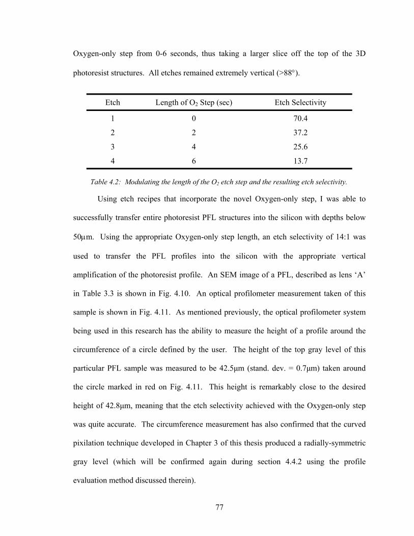
77
Oxygen-only step from 0-6 seconds, thus taking a larger slice off the top of the 3D
photoresist structures. All etches remained extremely vertical (>88°).
Etch Length of O2 Step (sec) Etch Selectivity
1 0 70.4
2 2 37.2
3 4 25.6
4 6 13.7
Table 4.2: Modulating the length of the O2 etch step and the resulting etch selectivity.
Using etch recipes that incorporate the novel Oxygen-only step, I was able to
successfully transfer entire photoresist PFL structures into the silicon with depths below
50µm. Using the appropriate Oxygen-only step length, an etch selectivity of 14:1 was
used to transfer the PFL profiles into the silicon with the appropriate vertical
amplification of the photoresist profile. An SEM image of a PFL, described as lens ‘A’
in Table 3.3 is shown in Fig. 4.10. An optical profilometer measurement taken of this
sample is shown in Fig. 4.11. As mentioned previously, the optical profilometer system
being used in this research has the ability to measure the height of a profile around the
circumference of a circle defined by the user. The height of the top gray level of this
particular PFL sample was measured to be 42.5µm (stand. dev. = 0.7µm) taken around
the circle marked in red on Fig. 4.11. This height is remarkably close to the desired
height of 42.8µm, meaning that the etch selectivity achieved with the Oxygen-only step
was quite accurate. The circumference measurement has also confirmed that the curved
pixilation technique developed in Chapter 3 of this thesis produced a radially-symmetric
gray level (which will be confirmed again during section 4.4.2 using the profile
evaluation method discussed therein).
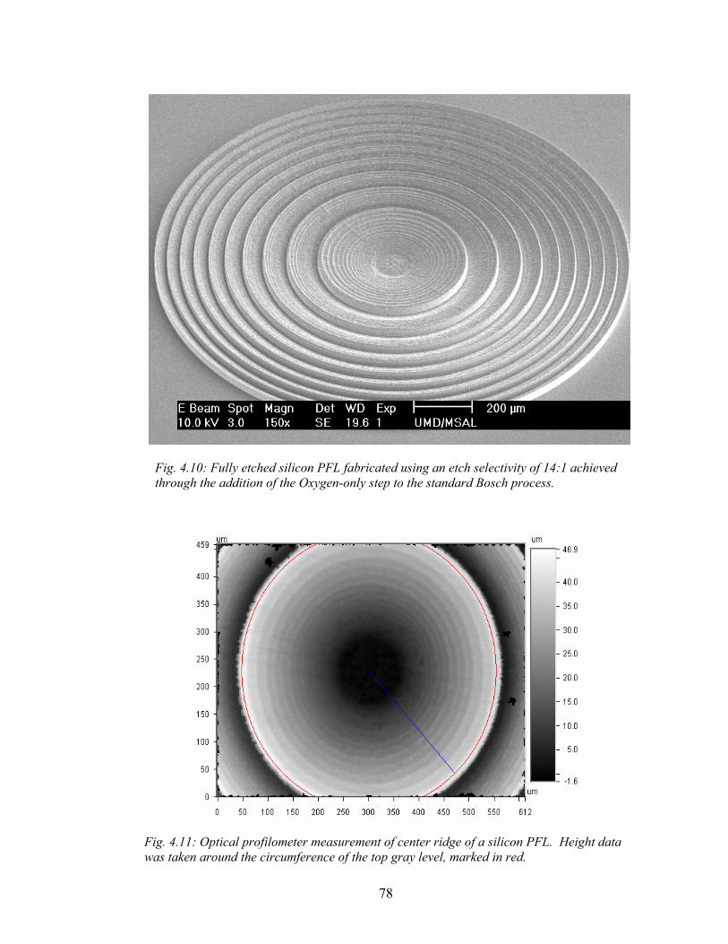
78
Fig. 4.10: Fully etched silicon PFL fabricated using an etch selectivity of 14:1 achieved through the addition of the Oxygen-only step to the standard Bosch process.
Fig. 4.11: Optical profilometer measurement of center ridge of a silicon PFL. Height data was taken around the circumference of the top gray level, marked in red.
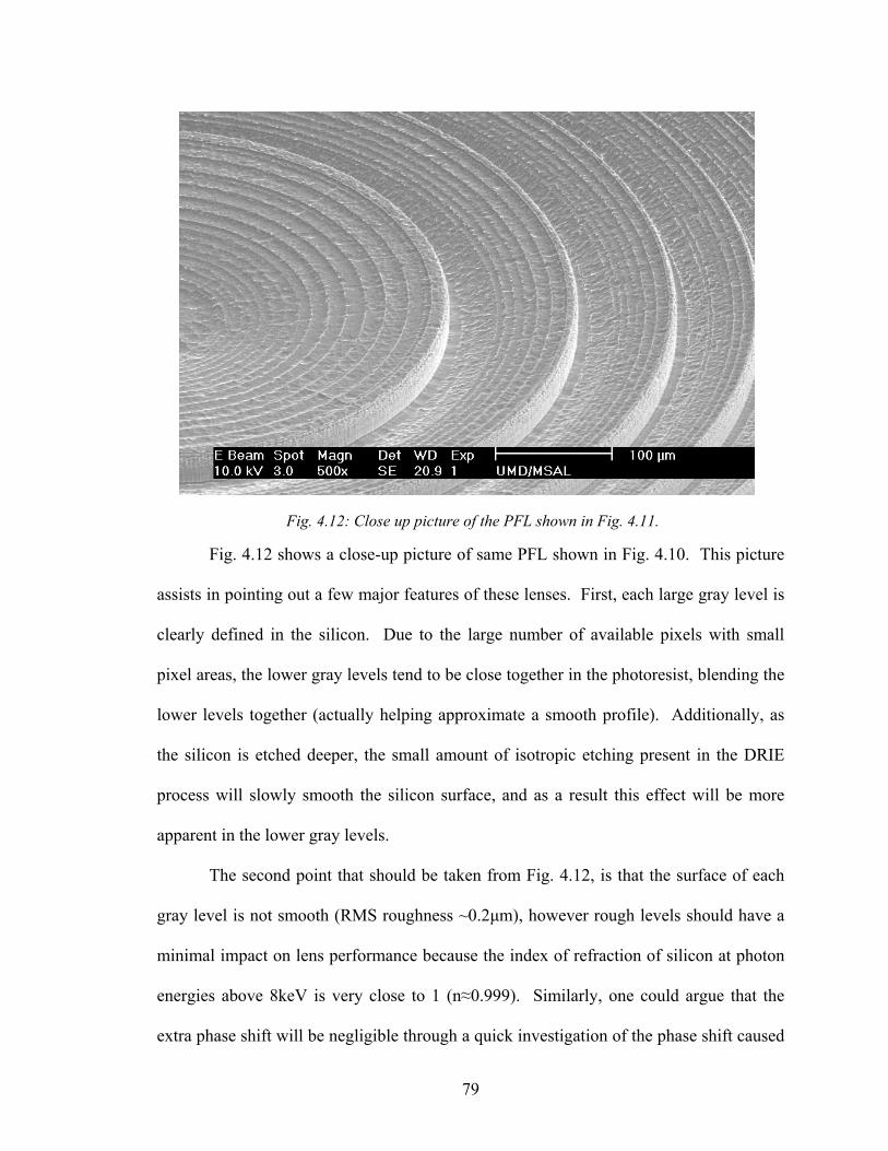
79
Fig. 4.12 shows a close-up picture of same PFL shown in Fig. 4.10. This picture
assists in pointing out a few major features of these lenses. First, each large gray level is
clearly defined in the silicon. Due to the large number of available pixels with small
pixel areas, the lower gray levels tend to be close together in the photoresist, blending the
lower levels together (actually helping approximate a smooth profile). Additionally, as
the silicon is etched deeper, the small amount of isotropic etching present in the DRIE
process will slowly smooth the silicon surface, and as a result this effect will be more
apparent in the lower gray levels.
The second point that should be taken from Fig. 4.12, is that the surface of each
gray level is not smooth (RMS roughness ~0.2µm), however rough levels should have a
minimal impact on lens performance because the index of refraction of silicon at photon
energies above 8keV is very close to 1 (n≈0.999). Similarly, one could argue that the
extra phase shift will be negligible through a quick investigation of the phase shift caused
Fig. 4.12: Close up picture of the PFL shown in Fig. 4.11.
80
in silicon at X-ray energies. If 8.4keV photons are considered, the thickness of silicon
required to produce a 2π phase shift, using equation (1.2), is 21.4µm. If a local section of
the lens has an extra 0.2µm of silicon (due to roughness), the extra phase shift introduced
is slightly less than 1%. Since a step approximation to the ideal profile is already being
made, an extra 1% phase shift may actually help performance if the step is inducing a
non-ideal phase shift at that point anyway. Although the presence of surface roughness on
gray levels will be a concern as gray-scale technology is developed for other applications,
the surface roughness currently on our PFL structures is acceptable. Should the surface
roughness become unacceptable or cause unforeseen effects, it could possibly be reduced
using an isotropic etch, or a thermal oxidation and strip, which will be discussed further
in Chapter 5.
A final feature to notice in Fig. 4.12 is that the backside of each ridge is sharply
defined. As discussed earlier, optical profilometry is the only method available to
measure the profile in these deeply etched silicon areas with vertical sidewalls. These
measurements taken with an optical profilometer have helped quantify another
characteristic of our etch recipes, namely that as the ridge width is decreased, the final
etch depth in silicon decreases as well. This phenomenon is known as Aspect Ratio
Dependent Etching (ARDE) and is discussed in more detail in the following section.
4.3.3. Aspect Ratio Dependent Etching
Aspect Ratio Dependent Etching (ARDE) can be observed in virtually any RIE or
DRIE application. As discussed in Chapter 2, the majority of the etching in a dry plasma
process is driven by chemical reactions. Therefore, the reactive species and ions present
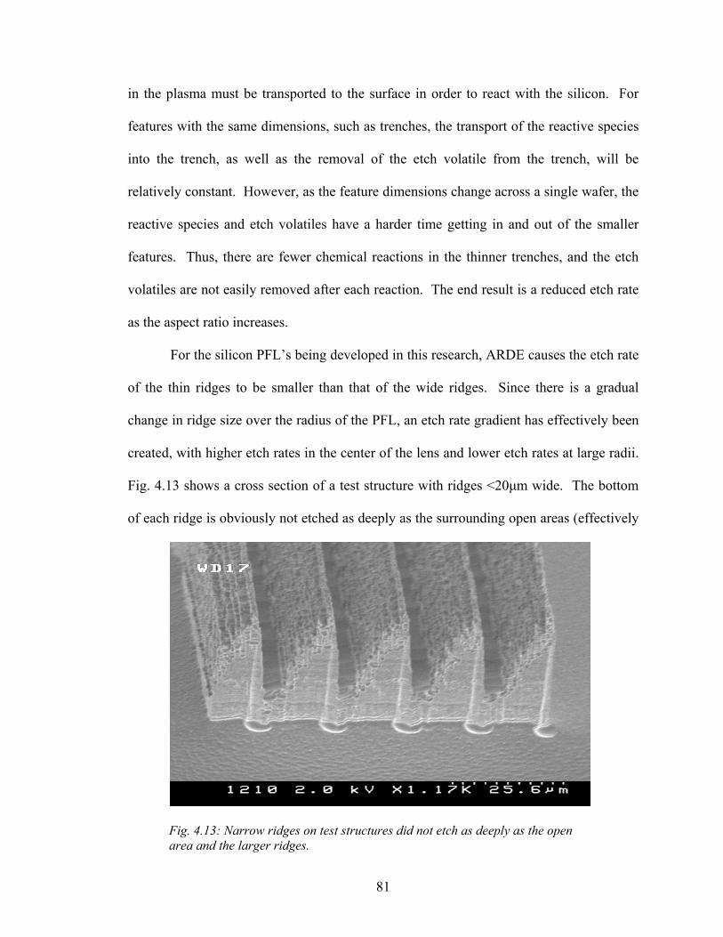
81
in the plasma must be transported to the surface in order to react with the silicon. For
features with the same dimensions, such as trenches, the transport of the reactive species
into the trench, as well as the removal of the etch volatile from the trench, will be
relatively constant. However, as the feature dimensions change across a single wafer, the
reactive species and etch volatiles have a harder time getting in and out of the smaller
features. Thus, there are fewer chemical reactions in the thinner trenches, and the etch
volatiles are not easily removed after each reaction. The end result is a reduced etch rate
as the aspect ratio increases.
For the silicon PFL’s being developed in this research, ARDE causes the etch rate
of the thin ridges to be smaller than that of the wide ridges. Since there is a gradual
change in ridge size over the radius of the PFL, an etch rate gradient has effectively been
created, with higher etch rates in the center of the lens and lower etch rates at large radii.
Fig. 4.13 shows a cross section of a test structure with ridges <20µm wide. The bottom
of each ridge is obviously not etched as deeply as the surrounding open areas (effectively
Fig. 4.13: Narrow ridges on test structures did not etch as deeply as the open area and the larger ridges.
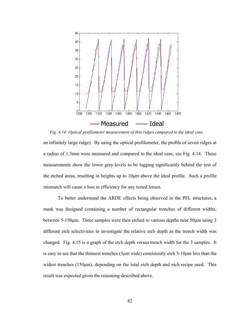
82
an infinitely large ridge). By using the optical profilometer, the profile of seven ridges at
a radius of 1.3mm were measured and compared to the ideal case, see Fig. 4.14. These
measurements show the lower gray-levels to be lagging significantly behind the rest of
the etched areas, resulting in heights up to 10µm above the ideal profile. Such a profile
mismatch will cause a loss in efficiency for any tested lenses.
To better understand the ARDE effects being observed in the PFL structures, a
mask was designed containing a number of rectangular trenches of different widths,
between 5-150µm. Three samples were then etched to various depths near 50µm using 3
different etch selectivities to investigate the relative etch depth as the trench width was
changed. Fig. 4.15 is a graph of the etch depth versus trench width for the 3 samples. It
is easy to see that the thinnest trenches (5µm wide) consistently etch 5-10µm less than the
widest trenches (150µm), depending on the total etch depth and etch recipe used. This
result was expected given the reasoning described above.
IdealMeasuredFig. 4.14: Optical profilometer measurement of thin ridges compared to the ideal case.
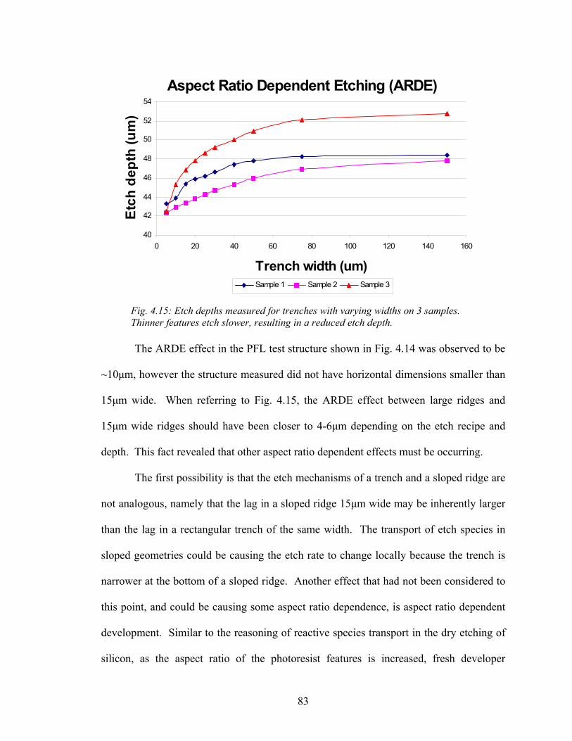
83
The ARDE effect in the PFL test structure shown in Fig. 4.14 was observed to be
~10µm, however the structure measured did not have horizontal dimensions smaller than
15µm wide. When referring to Fig. 4.15, the ARDE effect between large ridges and
15µm wide ridges should have been closer to 4-6µm depending on the etch recipe and
depth. This fact revealed that other aspect ratio dependent effects must be occurring.
The first possibility is that the etch mechanisms of a trench and a sloped ridge are
not analogous, namely that the lag in a sloped ridge 15µm wide may be inherently larger
than the lag in a rectangular trench of the same width. The transport of etch species in
sloped geometries could be causing the etch rate to change locally because the trench is
narrower at the bottom of a sloped ridge. Another effect that had not been considered to
this point, and could be causing some aspect ratio dependence, is aspect ratio dependent
development. Similar to the reasoning of reactive species transport in the dry etching of
silicon, as the aspect ratio of the photoresist features is increased, fresh developer
Aspect Ratio Dependent Etching (ARDE)
40
42
44
46
48
50
52
54
0 20 40 60 80 100 120 140 160
Trench width (um)
Etch
dep
th (u
m)
Sample 1 Sample 2 Sample 3
Fig. 4.15: Etch depths measured for trenches with varying widths on 3 samples. Thinner features etch slower, resulting in a reduced etch depth.
84
solution will have a harder time getting in and out of the smaller features to remove the
exposed photoresist. Therefore, photoresist gray levels located in thin trenches may not
be developed as efficiently, resulting in slightly higher photoresist heights. The
investigation of these two effects will become increasingly important as the diameter of
the PFL is increased, however such investigations fall beyond the scope of this thesis. A
solution that has prospects for diminishing, and possibly eliminating, the aspect ratio
effects seen in final silicon PFLs will be discussed in Chapter 5 as part of the future work.
4.4. Profile Evaluation (Silicon)
Now that 3D silicon PFL profiles have been successfully designed and fabricated,
a quantitative method must be developed by which the final silicon profile may be
evaluated. A new X-ray beam line testing facility is currently under construction at
NASA-Goddard Space Flight Center (near the University of Maryland campus), but until
the facility is operational, a simple method with the ability to calculate an approximate
theoretical PFL efficiency will greatly assist in evaluating each design and fabrication
iteration. The following sections will describe the method developed in this research to
calculate an expected lens efficiency using simple physical principles. Efficiencies
calculated from perfect stepped lens profiles (binary, 4-level, etc) will be shown to agree
well with the theoretical efficiencies calculated using equation (1.1). Measurements of
silicon profiles will then be used to calculate the expected efficiency of a variety of
lenses, including those lenses fabricated using etch recipes with the incorrect etch
selectivity. Finally, comments will be made regarding the differences in calculated
efficiency for the 3 primary lenses described in Table 3.3.
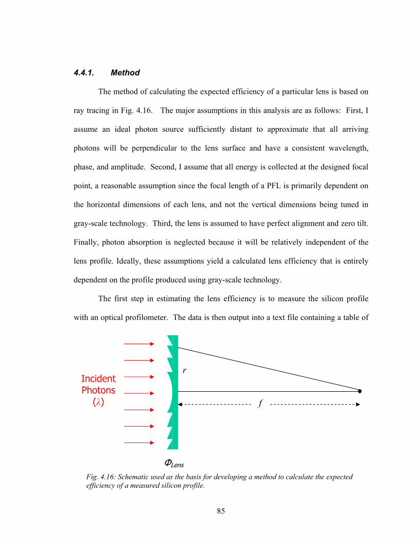
85
4.4.1. Method
The method of calculating the expected efficiency of a particular lens is based on
ray tracing in Fig. 4.16. The major assumptions in this analysis are as follows: First, I
assume an ideal photon source sufficiently distant to approximate that all arriving
photons will be perpendicular to the lens surface and have a consistent wavelength,
phase, and amplitude. Second, I assume that all energy is collected at the designed focal
point, a reasonable assumption since the focal length of a PFL is primarily dependent on
the horizontal dimensions of each lens, and not the vertical dimensions being tuned in
gray-scale technology. Third, the lens is assumed to have perfect alignment and zero tilt.
Finally, photon absorption is neglected because it will be relatively independent of the
lens profile. Ideally, these assumptions yield a calculated lens efficiency that is entirely
dependent on the profile produced using gray-scale technology.
The first step in estimating the lens efficiency is to measure the silicon profile
with an optical profilometer. The data is then output into a text file containing a table of
Fig. 4.16: Schematic used as the basis for developing a method to calculate the expected efficiency of a measured silicon profile.
r
ФLens
f
Incident Photons
(λ)
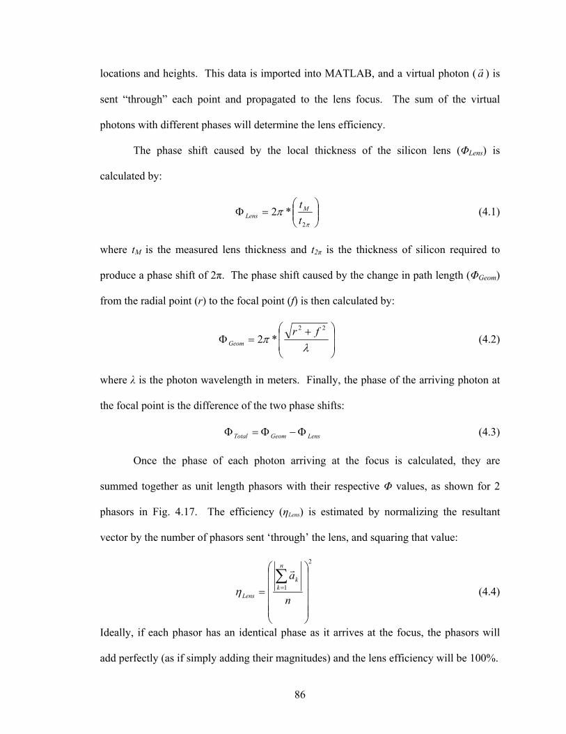
86
locations and heights. This data is imported into MATLAB, and a virtual photon ( ar ) is
sent “through” each point and propagated to the lens focus. The sum of the virtual
photons with different phases will determine the lens efficiency.
The phase shift caused by the local thickness of the silicon lens (ΦLens) is
calculated by:
=Φ
π
π2
*2ttM
Lens (4.1)
where tM is the measured lens thickness and t2π is the thickness of silicon required to
produce a phase shift of 2π. The phase shift caused by the change in path length (ΦGeom)
from the radial point (r) to the focal point (f) is then calculated by:
+=Φ
λπ
22
*2fr
Geom (4.2)
where λ is the photon wavelength in meters. Finally, the phase of the arriving photon at
the focal point is the difference of the two phase shifts:
LensGeomTotal Φ−Φ=Φ (4.3)
Once the phase of each photon arriving at the focus is calculated, they are
summed together as unit length phasors with their respective Φ values, as shown for 2
phasors in Fig. 4.17. The efficiency (ηLens) is estimated by normalizing the resultant
vector by the number of phasors sent ‘through’ the lens, and squaring that value:
2
1
=∑=
n
an
kk
Lens
r
η (4.4)
Ideally, if each phasor has an identical phase as it arrives at the focus, the phasors will
add perfectly (as if simply adding their magnitudes) and the lens efficiency will be 100%.
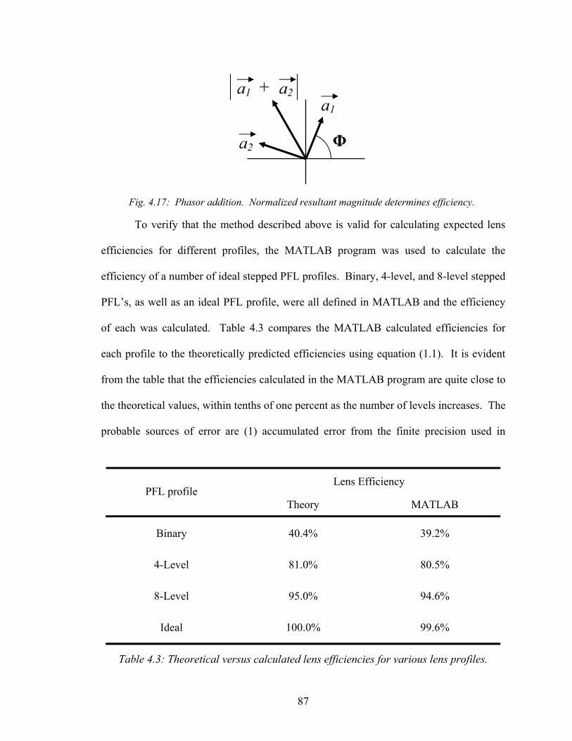
87
To verify that the method described above is valid for calculating expected lens
efficiencies for different profiles, the MATLAB program was used to calculate the
efficiency of a number of ideal stepped PFL profiles. Binary, 4-level, and 8-level stepped
PFL’s, as well as an ideal PFL profile, were all defined in MATLAB and the efficiency
of each was calculated. Table 4.3 compares the MATLAB calculated efficiencies for
each profile to the theoretically predicted efficiencies using equation (1.1). It is evident
from the table that the efficiencies calculated in the MATLAB program are quite close to
the theoretical values, within tenths of one percent as the number of levels increases. The
probable sources of error are (1) accumulated error from the finite precision used in
Lens Efficiency PFL profile
Theory MATLAB
Binary 40.4% 39.2%
4-Level 81.0% 80.5%
8-Level 95.0% 94.6%
Ideal 100.0% 99.6%
Table 4.3: Theoretical versus calculated lens efficiencies for various lens profiles.
Φ
a1
a1 a2
a2
Fig. 4.17: Phasor addition. Normalized resultant magnitude determines efficiency.
88
MATLAB (16 decimal places), and (2) the lens profile equations already contains a slight
approximation since the constant coefficient in equation (3.2) is only carried to 1 decimal
place. For the purposes of this research, Table 4.3 confirms the method of calculating
lens efficiency described in this section is sufficient to evaluate each silicon PFL profile.
4.4.2. Profile Measurements
As mentioned before, an optical profilometer scan of a particular silicon PFL will
be taken to obtain a list of radial locations in ‘x’ and heights in ‘y.’ One problem that
became apparent as these measurements progressed was the definition of a common
origin. The optical profilometer takes the origin of the scan to be the first data point,
however the first data point (x=0) is almost certainly not actually located at the exact
center (r=0) of the lens design. Thus the entire measured profile must be shifted until
each ‘x’ point has been translated to correspond to the appropriate ‘r’ on the lens design.
To accommodate this, the MATLAB program was modified to sweep through a large
range of offsets and calculate the lens efficiency with each offset. When the measured
profile is shifted the appropriate amount, the lens efficiency should be at a maximum.
An example optical profilometer 3D measurement is shown in Fig. 4.18. Once
each measurement is taken, an arbitrary “SCAN” may be defined with any direction and
length. The 2-D data is output to a text file. Table 4.4 shows the resulting efficiency for
5 scans taken on a single 3D measurement. Each scan began at the center of the lens and
scanned at the specified angles for the first 3 ridges (angles are approximate, and
measured from a horizontal line across the width of the page). The calculated
efficiencies for these 5 scans are grouped quite closely. Thus, within a small amount of
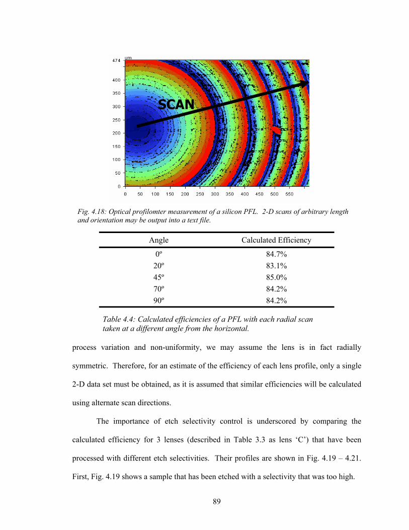
89
process variation and non-uniformity, we may assume the lens is in fact radially
symmetric. Therefore, for an estimate of the efficiency of each lens profile, only a single
2-D data set must be obtained, as it is assumed that similar efficiencies will be calculated
using alternate scan directions.
The importance of etch selectivity control is underscored by comparing the
calculated efficiency for 3 lenses (described in Table 3.3 as lens ‘C’) that have been
processed with different etch selectivities. Their profiles are shown in Fig. 4.19 – 4.21.
First, Fig. 4.19 shows a sample that has been etched with a selectivity that was too high.
Angle Calculated Efficiency
0º 84.7% 20º 83.1% 45º 85.0% 70º 84.2% 90º 84.2%
Table 4.4: Calculated efficiencies of a PFL with each radial scan taken at a different angle from the horizontal.
SCAN
Fig. 4.18: Optical profilomter measurement of a silicon PFL. 2-D scans of arbitrary length and orientation may be output into a text file.
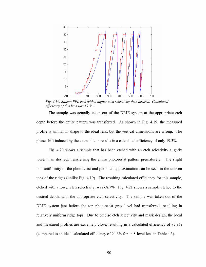
90
The sample was actually taken out of the DRIE system at the appropriate etch
depth before the entire pattern was transferred. As shown in Fig. 4.19, the measured
profile is similar in shape to the ideal lens, but the vertical dimensions are wrong. The
phase shift induced by the extra silicon results in a calculated efficiency of only 19.3%.
Fig. 4.20 shows a sample that has been etched with an etch selectivity slightly
lower than desired, transferring the entire photoresist pattern prematurely. The slight
non-uniformity of the photoresist and pixilated approximation can be seen in the uneven
tops of the ridges (unlike Fig. 4.19). The resulting calculated efficiency for this sample,
etched with a lower etch selectivity, was 68.7%. Fig. 4.21 shows a sample etched to the
desired depth, with the appropriate etch selectivity. The sample was taken out of the
DRIE system just before the top photoresist gray level had transferred, resulting in
relatively uniform ridge tops. Due to precise etch selectivity and mask design, the ideal
and measured profiles are extremely close, resulting in a calculated efficiency of 87.9%
(compared to an ideal calculated efficiency of 94.6% for an 8-level lens in Table 4.3).
Fig. 4.19: Silicon PFL etch with a higher etch selectivity than desired. Calculated efficiency of this lens was 19.3%
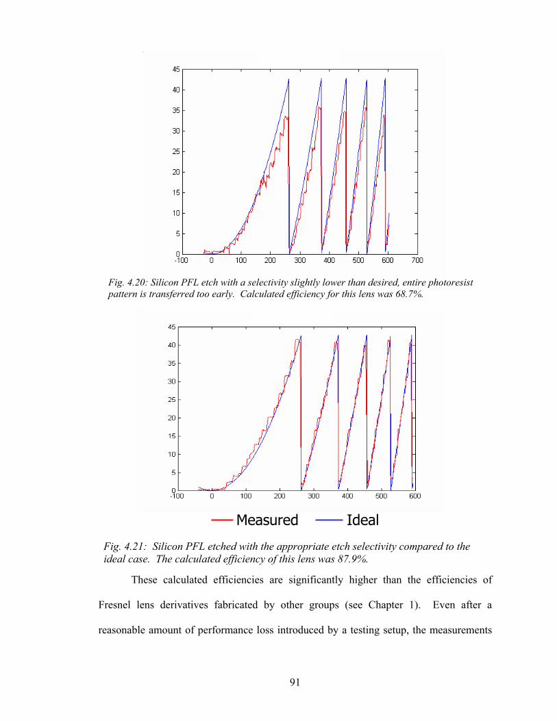
91
These calculated efficiencies are significantly higher than the efficiencies of
Fresnel lens derivatives fabricated by other groups (see Chapter 1). Even after a
reasonable amount of performance loss introduced by a testing setup, the measurements
IdealMeasured
Fig. 4.21: Silicon PFL etched with the appropriate etch selectivity compared to the ideal case. The calculated efficiency of this lens was 87.9%.
Fig. 4.20: Silicon PFL etch with a selectivity slightly lower than desired, entire photoresist pattern is transferred too early. Calculated efficiency for this lens was 68.7%.
92
presented above should provide a good starting point for estimating the lens performance
in an X-ray beam line. It must be noted that the efficiencies quoted above are only
accurate for a lens with a radius equal to the scan length. As the lens radius increases,
the outer ridges will become progressively less efficient because of the ARDE effect
discussed previously, lowering lens performance.
Die Calculated Efficiency
2 84.8% 4 87.3% 5 86.4% 6 87.9% 8 83.1%
Table 4.5: Calculated efficiencies of PFLs at different locations across a 75mm wafer.
Since the demonstration of the imaging properties of a PFL may be accomplished
with a small number of high quality PFL’s, it is not necessary to produce large quantities
of identical lenses. Nonetheless, uniformity is a chief concern for the integration of gray-
scale technology into other applications. If the uniformity can be controlled sufficiently,
coded PFL arrays may be possible to investigate alternative high energy telescope
arrangements. Table 4.5 shows the calculated efficiency of 5 PFLs (lens ‘C’ in Table
3.3) at 5 different locations on a 75mm wafer. The range in efficiencies is <5% across
the wafer. With further process optimization, PFL uniformity across the wafer should
improve slightly. These high efficiencies should be sufficient to enable coded PFL
arrays.
Returning to the ARDE issue, I am now able to quantify the effective decrease in
efficiency resulting from the reduced etch rate seen in smaller ridges. The efficiency for
the structures shown in Fig. 4.14 was calculated to be only 57%, while the center of the
93
same lens was calculated to have an efficiency of over 85%. Thus, the ARDE problem
must be improved before PFLs of increased radius with high efficiency can be
realistically fabricated. A possible solution will be outlined in Chapter 5 of this thesis as
part of the discussion on future work
4.4.3. Lens design comparison
Finally, the method of calculating profile efficiency is used here to compare and
contrast 2 main parameters used in the optical mask design for the lenses described in
Table 3.3. First, the accuracy of the Gaussian approximation and the choice of a pixel set
will be discussed as they effect the calculated efficiency, using lens designs ‘A’ and ‘B’.
Second, lens designs ‘B’ and ‘C’ will be used to investigate the difference in calculated
efficiency resulting from using a different number of gray levels to fabricate each ridge.
The difference in calculated efficiency at the outer edges of each lens will not be directly
compared due to the non-linear ARDE effects that have already been discussed at length
and are not a product of the optical mask design.
Referring back to Table 3.3, lens ‘A’ and ‘B’ have identical focal lengths, etch
depths, and number of levels. The main differences between these two lenses are the lens
diameter and the Gaussian approximation. In the Gaussian approximation, the fit
parameters, A0 and γ, are slightly different for the two lenses, and although the number of
levels used were the same, the pixel sets were different. By measuring only the inner
600µm profile, we are able to isolate the effect on the calculated efficiency from
improving the Gaussian approximation and pixel set. Fig. 4.22 shows an optical
profilometer measurement of lens ‘A’ which had a calculated efficiency of 66.5%. Fig.
94
4.23 shows an optical profilometer measurement of lens ‘B’ which had a calculated
efficiency of 81.7%. Thus, by improving the accuracy of the Gaussian approximation
and the pixel set, an increase in calculated efficiency of roughly 15% was achieved.
The improvement in calculated efficiency is attributed to two primary factors:
First, as discussed in section 3.4.2, the pixel set used to fabricate lens ‘B’ did not include
some of the larger pixels whose Tr values had large separations. Looking at Fig. 4.22,
the top 3-4 levels are spaced quite far apart (vertically) while the bottom levels are
bunched together. By replacing the low Tr pixels with pixels having intermediate Tr
values, the levels may be evenly distributed, enabling higher lens efficiencies. Second,
now that the pixel set does not include the low Tr pixels, the Gaussian fit parameters
were adjusted to improve the curve fit for only the remaining pixels. Thus, the “bubble”
in the profile seen in the center of the first ridge in Fig. 4.22 is reduced in Fig. 4.23.
Further improving the accuracy of the Gaussian fit (as discussed in section 3.4.1) could
Fig. 4.22: Optical profilometer measurement of a silicon lens ‘A’ design versus the ideal case. Calculated efficiency of this lens was 66.5%.
IdealMeasured
95
eliminate any small remaining “bubble” in the profile, but the Gaussian/exponential form
of the approximation must be kept for easy integration into the mask layout design.
Comparing lens ‘B’ and lens ‘C’, they both use the more accurate Gaussian fit
parameters, and are designed for identical focal lengths and etch depths. The primary
differences are again in the lens diameter, which will be ignored by only measuring the
center of the lens, and in the number of gray levels used to approximate the profile. Lens
‘B’ utilizes 32 total gray levels, or 16 levels per phase depth, while lens ‘C’ utilizes half
as many gray levels, 16 total and 8 per phase depth. Again, lens ‘B’ with an efficiency of
81.7% is shown in Fig. 4.23 and lens ‘C’ with an efficiency of 87.9% was shown
previously in Fig. 4.21.
In comparing the two figures, it can be seen that the height of lens ‘B’ was just
shy of the height of lens ‘C,’ which would contribute to some of the difference in
calculated efficiency. However, these structures were both located on the same wafer
and underwent the same processing steps, and are typical examples of the structures seen
Fig. 4.23: Optical profilometer measurement of a silicon lens ‘B’ design versus the ideal case. Calculated efficiency of this lens was 81.7%.
IdealMeasured
96
across the wafer. The primary conclusion I would like to draw from these two designs is
that there is no significant gain in the calculated efficiency of profiles designed using 16
levels per phase depth versus 8 levels per phase depth. (The theoretical efficiency
difference between ideal 16 level and 8 level designs using equation (1.1) would be
98.7% vs. 95.0%). In fact, the lens ‘C’ structures (with only 8 levels per phase depth) on
a single wafer had calculated efficiencies that were consistently ~5% more efficient than
the lens ‘B’ structures on the same wafer (16 levels per phase depth). One possible
reason for lens ‘C’ to have equal to or higher efficiencies is that larger gray levels are
more sharply defined and thus retain their expected heights with greater integrity.
Additionally, as the width of the ridges is decreased, it will no longer be possible to fit
every pixel in every ridge. This limitation means that as the radius increases, even
though there are 16 pixels per phase depth available, not all levels will be used in thin
ridges, and we are essentially forced into an 8 level per phase depth design.
In summation, both lens ‘B’ and lens ‘C’ have significantly higher calculated
efficiencies than lens ‘A’, and the calculated efficiency of the lens ‘C’ design is
consistently equal to or higher than the lens ‘B’ design, even though lens ‘B’ utilizes a
larger number of gray levels. Since ridge widths decrease as the PFL radius increases,
not every level in the larger gray level set will be used in each ridge, essentially reducing
a large gray level set into a smaller gray level set. Therefore, I conclude that gray-scale
PFL designs using more than 8 gray levels per phase depth will exhibit a negligible gain
in efficiency, if any at all.
97
4.5. Summary
This chapter has presented all fabrication aspects of developing a silicon PFL
using gray-scale technology. Lithography results were obtained showing the successful
fabrication of photoresist PFL structures. Limitations were discussed regarding the
intensity profiles created as the ridge dimensions are reduced and fewer pixels are used to
define each ridge. Optical profilometer measurements of photoresist profiles confirmed
that the Gaussian approximation method introduced in Chapter 3 of this thesis is indeed a
valid method for accurately defining 3D photoresist profiles. Pattern transfer of the 3D
photoresist structures with extremely low etch selectivity was achieved through the
introduction of a novel Oxygen-only etch step to the standard Bosch process. By
modulating the length of the Oxygen-only step, the etch selectivity may be tuned over a
wide range without large effects on other etch characteristics. Finally, a method was
developed to estimate the efficiency of different silicon PFL profiles measured with an
optical profilometer. These calculated efficiencies were used to evaluate and compare
the different designs and fabrication steps developed in this thesis. Chapter 5 will
summarize the work presented in the first 4 chapters, as well as discuss areas of design
and fabrication that will be addressed as part of the future work involved in this research.
98
5. Summary and Future Work
5.1. Summary
This thesis has outlined the steps taken to develop a phase Fresnel lens in silicon
with modest focal lengths (~100m) for soft X-ray energies using gray-scale technology.
PFLs fabricated with this technology have the potential to exhibit high angular resolution
and high efficiency, as well as serve as the basis of an investigation into larger space-
bound PFL telescopes for gamma-ray energies. Further development of the techniques
and issues discussed in this thesis should produce PFLs appropriate for testing in an
existing X-ray beam line at NASA XRCF in Huntsville, Al, or a beam line currently
under construction at NASA Goddard Space Flight Center (GSFC) in Greenbelt, MD. If
ground tests of a silicon PFL are successful, and high angular resolution and high
efficiency are achieved, then we will have taken the first step towards a high efficiency
PFL telescope with the ability to probe nearby active galactic nuclei, event horizons
around black holes, and other high energy phenomena with unprecedented accuracy.
The fabrication of the PFL’s presented in this thesis was achieved through the use
of gray-scale lithography and deep reactive ion etching (DRIE), two MEMS fabrication
techniques. Gray-scale lithography enables complex 3D structures to be fabricated in one
lithography step using standard processing equipment. By manipulating the placement of
various sized opaque pixels on an optical mask, an intensity pattern is generated on the
photoresist surface that will form the 3D structure in the photoresist after development.
This 3D photoresist structure is then transferred into a silicon substrate using DRIE to
create the final silicon structure.
99
Analysis was presented regarding the design of individual pixels given mask
fabrication limitations, and the construction of a pixel set as it effects the design and
fabrication of a PFL. Millions of pixels are required to produce any particular structure,
and each must be selected and placed with high accuracy using an automated system. A
solution to this problem was the development of the Gaussian approximation method,
introduced in Chapter 3. Based on a calibration mask, the Gaussian approximation
enables a simple relation between the pixel size and the corresponding height in
photoresist on the wafer. This relationship is easily reversed to calculate the pixel size
required to produce a desired photoresist height. A C-program queries each pixel
location, and using the desired PFL profile as an input, selects the pixel with a size
closest to ideal. Since the intensity pattern is generated by pixels of finite width, a digital
nature of the approximation was apparent in the photoresist, causing non-uniform
photoresist profiles of thinner ridges. To minimize this effect, the PFL design was
modified to incorporate a 4π phase depth. The primary advantage of a deeper phase
depth design is that the width of each ridge is essentially doubled in the photoresist,
making it easier to achieve a uniform gradient intensity profile. An additional advantage
of selecting an increased phase depth design is that the required etch depth is larger,
increasing the necessary etch selectivity (helpful considering the low etch selectivity
already required to transfer an entire 3D photoresist pattern in shallow depths).
Achieving the proper etch selectivity is paramount to the success of gray-scale
technology. As such, the DRIE system at ARL was characterized by varying a number of
DRIE etch recipe parameters in the standard Bosch process in an attempt to change and
control the etch selectivity. Although the etch selectivity was modulated, it was often at
100
the expense of other etch properties, such as sidewall profile, and the etch selectivity was
still not low enough. The desired etch depth of a 4π phase depth design (43µm) required
an etch selectivity of 20 or below (assuming 2-3µm resist), so the etch selectivity had to
be decreased dramatically by a new method. In this thesis, I therefore introduced the
concept of a modified Bosch process with an Oxygen-only step. This modified process
adds an additional step to the Bosch cycle, which uses an Oxygen plasma to increase the
etch rate of the photoresist and not the silicon, thus decreasing the etch selectivity. Using
this new process, recipes with low etch selectivity were achieved. Furthermore, by
simply modulating the length of the oxygen step, the etch selectivity could be tuned over
a wide range without significant effect on sidewall profile.
Once PFL profiles had been fabricated, metrology methods for measuring both
photoresist and silicon profiles were discussed. Contact profilometry was deemed
appropriate for measuring photoresist profiles before pattern transfer into the silicon since
it does not disturb the photoresist profile. Optical profilometry was then used to measure
the high aspect ratio ridges of each silicon PFL after DRIE that could not be measured
with contact profilometry. Ray-tracing was employed to develop a method of estimating
PFL efficiency from a silicon profile. This method was shown to agree well with
theoretical predictions of ideal stepped profiles. Optical profilometer measurements were
subsequently imported into a mathematical programming tool (MATLAB) to calculate
the expected efficiency of each silicon profile.
The maximum calculated efficiency of a measured 8 level per phase depth gray-
scale profile was 87.9% (an ideal 8 level per phase depth profile has a maximum
calculated efficiency of 94.6%). Thus, the PFLs developed in this thesis should exhibit a
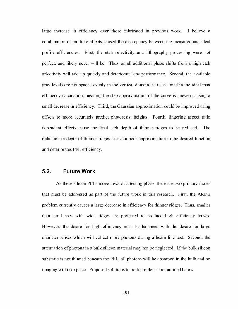
101
large increase in efficiency over those fabricated in previous work. I believe a
combination of multiple effects caused the discrepancy between the measured and ideal
profile efficiencies. First, the etch selectivity and lithography processing were not
perfect, and likely never will be. Thus, small additional phase shifts from a high etch
selectivity will add up quickly and deteriorate lens performance. Second, the available
gray levels are not spaced evenly in the vertical domain, as is assumed in the ideal max
efficiency calculation, meaning the step approximation of the curve is uneven causing a
small decrease in efficiency. Third, the Gaussian approximation could be improved using
offsets to more accurately predict photoresist heights. Fourth, lingering aspect ratio
dependent effects cause the final etch depth of thinner ridges to be reduced. The
reduction in depth of thinner ridges causes a poor approximation to the desired function
and deteriorates PFL efficiency.
5.2. Future Work
As these silicon PFLs move towards a testing phase, there are two primary issues
that must be addressed as part of the future work in this research. First, the ARDE
problem currently causes a large decrease in efficiency for thinner ridges. Thus, smaller
diameter lenses with wide ridges are preferred to produce high efficiency lenses.
However, the desire for high efficiency must be balanced with the desire for large
diameter lenses which will collect more photons during a beam line test. Second, the
attenuation of photons in a bulk silicon material may not be neglected. If the bulk silicon
substrate is not thinned beneath the PFL, all photons will be absorbed in the bulk and no
imaging will take place. Proposed solutions to both problems are outlined below.
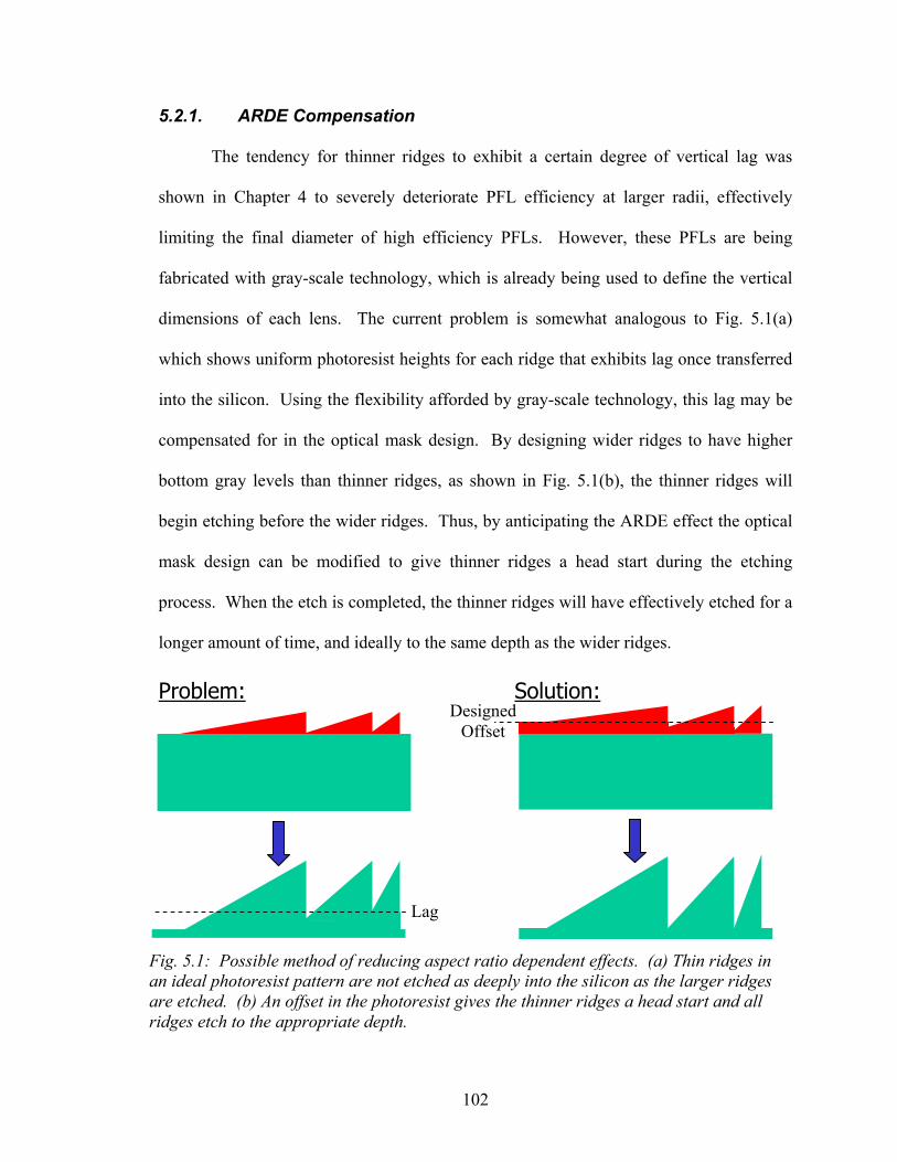
102
5.2.1. ARDE Compensation
The tendency for thinner ridges to exhibit a certain degree of vertical lag was
shown in Chapter 4 to severely deteriorate PFL efficiency at larger radii, effectively
limiting the final diameter of high efficiency PFLs. However, these PFLs are being
fabricated with gray-scale technology, which is already being used to define the vertical
dimensions of each lens. The current problem is somewhat analogous to Fig. 5.1(a)
which shows uniform photoresist heights for each ridge that exhibits lag once transferred
into the silicon. Using the flexibility afforded by gray-scale technology, this lag may be
compensated for in the optical mask design. By designing wider ridges to have higher
bottom gray levels than thinner ridges, as shown in Fig. 5.1(b), the thinner ridges will
begin etching before the wider ridges. Thus, by anticipating the ARDE effect the optical
mask design can be modified to give thinner ridges a head start during the etching
process. When the etch is completed, the thinner ridges will have effectively etched for a
longer amount of time, and ideally to the same depth as the wider ridges.
Solution:Problem:
Fig. 5.1: Possible method of reducing aspect ratio dependent effects. (a) Thin ridges in an ideal photoresist pattern are not etched as deeply into the silicon as the larger ridges are etched. (b) An offset in the photoresist gives the thinner ridges a head start and all ridges etch to the appropriate depth.
Lag
Designed Offset
103
A starting point to compensate for the aspect ratio dependence can be found in the
ARDE measurements shown in Fig. 4.15. Although these measurements are for
rectangular trenches, and will not account for geometrical effects, Fig. 4.15 does exhibit
the fact that the severity of the ARDE effect changes with trench width. Thus, any
calibration solution must be a continuous function of radius because a PFL profile
exhibits a continuous change in ridge width as the radius increases.
5.2.2. Bulk Silicon Removal
Due to the photon attenuation length of X-rays in silicon, the removal of the bulk
silicon substrate is essential for the eventual testing in an X-ray beam line of PFLs
fabricated using gray-scale technology. For the energies being considered in this thesis
(~10keV) the photon attenuation length is approximately 100µm. Therefore, a 400µm
thick wafer will block all incident photons before they reach the 40µm thick PFL on the
opposite side. A method of removing the bulk silicon selectively below the PFL is
proposed in Fig. 5.2. The starting material is a silicon-on-insulator (SOI) wafer, which
has two silicon layers separated by a thin silicon-dioxide layer, said to be ‘buried’
beneath the ‘device layer’, see Fig. 5.2(a). The thickness of the device layer can be
specified when ordering from a particular vendor, and should be selected to be slightly
larger than the thickness of the final PFL to be fabricated. Since the oxide layer is buried,
the gray-scale lithography process and the DRIE transfer should remain unchanged.
After PFL fabrication, a thermal oxidation step could be used to grow a thin
(~2000 angstrom) SiO2 layer over the entire wafer, as shown in Fig. 5.2(b). Using front-
to-back alignment, the SiO2 layer could be patterned on the backside to open windows
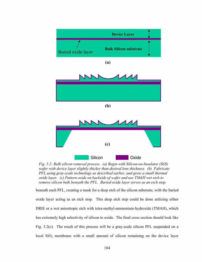
104
beneath each PFL, creating a mask for a deep etch of the silicon substrate, with the buried
oxide layer acting as an etch stop. This deep etch step could be done utilizing either
DRIE or a wet anisotropic etch with tetra-methyl-ammonium-hydroxide (TMAH), which
has extremely high selectivity of silicon to oxide. The final cross section should look like
Fig. 5.2(c). The result of this process will be a gray-scale silicon PFL suspended on a
local SiO2 membrane with a small amount of silicon remaining on the device layer
Silicon OxideFig. 5.2: Bulk silicon removal process. (a) Begin with Silicon-on-Insulator (SOI) wafer with device layer slightly thicker than desired lens thickness. (b) Fabricate PFL using gray-scale technology as described earlier, and grow a small thermal oxide layer. (c) Pattern oxide on backside of wafer and use TMAH wet etch to remove silicon bulk beneath the PFL. Buried oxide layer serves as an etch stop.
(c)
(b)
(a)
Device Layer
Bulk Silicon substrate Buried oxide layer
105
(which can be adjusted by buying wafers with the appropriate device layer thickness).
Thus, the absorption of the bulk silicon is minimized without losing the structural benefit
of a 400µm wafer for mounting and handling the lenses.
5.3. Conclusion
This thesis has successfully demonstrated gray scale technology as a valid method
for creating accurate 3D PFL profiles in silicon. A new Gaussian approximation method
has been introduced that is capable of defining complex profiles in a single lithography
step. Methods of tuning etch selectivity during DRIE were investigated, and a Bosch
process has been modified to include a unique Oxygen-only step to achieve uncommonly
low etch selectivities. Moreover, the techniques developed herein can be extended to any
application requiring precise definition of arbitrary 3D profiles in silicon. PFL profile
measurements were then combined with an analytical model to calculate the expected
efficiency of fabricated PFL profiles. The PFLs developed in this research have not yet
been tested in an X-ray beam line, however early measurements indicate that they should
perform with high efficiency in ground based testing. Such tests will set the stage for the
next generation of space-bound gamma-ray telescopes to be developed by NASA that
promise increases of many orders of magnitude in sensitivity and angular resolution.
106
BIBLIOGRAPHY
[1] Jerius, D., Donnelly, R. H., Tibbetts, M. S., et al, Proceedings of SPIE, p. 4012, 17
(2000)
[2] J. Koglin, F.E. Christensen, C.J. Hailey, F.A.C.P. Jensen, M. Sileo, D.L. Windt,
“Development and production of hard X-ray multiplayer optics for HEFT,”
Proceedings of SPIE, vol. 4851 (X-ray and Gamma-ray Telescopes and Instruments
for Astronomy), 4851-67 (2002).
[3] B. D. Ramsey et al, Development of hard x-ray optics at MSFC,” Proceedings of
SPIE, vol. 4851 (X-ray and Gamma-ray Telescopes and Instruments for
Astronomy), 4851-69 (2002).
[4] Y. Ogasaka et al, “Supermirror hard x-ray telescope and the results of first
observation flight of InFOCuS, Proceedings of SPIE, vol. 4851 (X-ray and Gamma-
ray Telescopes and Instruments for Astronomy), 4851-68 (2002).
[5] White, N.E. and Tananbaum, H., Astron. Nachr., 320, 280 (1999)
[6] M. D. Lieber, W. C. Cash, D. J. Gallagher, “System performance evaluation of the
MAXIM concept with integrated modeling,” Proceedings of SPIE, vol. 4851 (X-ray
and Gamma-ray Telescopes and Instruments for Astronomy), 4851-34 (2002).
[7] http://sci.esa.int/integral/ visited July 24, 2003
[8] http://glast.gsfc.nasa.gov/science/instruments/ visited October 7, 2003.
[9] G. Skinner. “Diffractive/refractive optics for high energy astronomy I. Gamma-ray
phase Fresnel lenses.” Astronomy and Astrophysics, v.375, p.691-700 (2001).
107
[10] G. Skinner, “Diffractive/refractive optics for high energy astronomy II: Variations
on the theme,” Astronomy and Astrophysics, v.383, p.352-9, Feb 2002.
[11] G. Skinner, P. von Ballmoos, H. Halloin, N. Gehrels, J. Krizmanic. “Diffraction-
limited gamma-ray imaging with Fresnel lenses.” Proceedings of SPIE v.4851, X-
ray and Gamma-Ray Telescopes and Instruments for Astronomy (J.E. Truemper &
H.D. Tananbaum, eds.), 4851-163 (2002).
[12] B. Hadimioglu, E. G. Rawson, R. Lujan, M. Lim, J. C. Zesch, B. T. Khuri-Yakub,
and C. F. Quate. “High-Efficiency Fresnel Acoustic Lenses,” 1993 Ultrasonics
Symposium, p. 579-82.
[13] J.R. Leger, M. L. Scott, P. Bundman and M. P. Griswold. “Astigmatic Wavefront
Correction of Gain-Guided Laser Diode Array Using Anamorphic Diffractive
Microlenses,” Proc. SPIE, v. 884, p.82 (1988).
[14] B. H. Kleemann and R. Guther, “Zonal diffraction efficiencies and imaging of
micro-Fresnel lenses,” Journal of Modern Optics, Vol. 45, No. 7, p. 1405-1420,
1998.
[15] NASA GSFC Integrated Mission Design Center (IMDC) study (2002, unpublished)
[16] Chantler, C.T., 1995, “Theoretical Form Factor, Attenuation and Scattering
Tabulation for Z=1-92 from E=1-20eV to E=0.4-1.0Mev” J. Phys. Chem. Ref. Data,
24,71.
[17] C. Linder, L. Paratte, M-A Gretillat, V.P. Jaeckllin, and N.F. de Rooij, “Surface
Micromachining,” J. Micromech. Microeng., vol. 2, pp. 122-132, 1992.
[18] G. T. A. Kovacs, N. I. Maluf, and K. E. Peterson, “ Bulk Micromachining of
Silicon,” Proc. IEEE, vol. 86, pp. 1536-1551, 1998.
108
[19] Robert Bosch GmbH, US patent 4,855,017
[20] S. Spector, C. J. Jacobsen, and D. M. Tennant, “Process optimization for production
of sub-20nm soft x-ray zone plates,” J. Vac. Sci. Technol. B 15(6), Nov/Dec
p.2872-6 1997.
[21] Z. Chen, et al. “Design and fabrication of fresnel zone plates with large numbers of
zones,” J. Vac. Sci. Technol. B 15(6), Nov/Dec p. 2522-7, 1997.
[22] E. Di Fabrizio and M. Gentili, “X-ray multilevel zone plate fabrication by means of
electron-beam lithography: Toward high-efficiency performances,” J. Vac. Sci.
Technol. B 17(6), Nov/Dec p. 3439-3443, 1999.
[23] A. Bertsch, H. Lorenz, and P. Renaud, “Combining Microstereolithography and
Thick Resist UV Lithography for 3D Microfabrication,” Proc. of IEEE: MEMS ’98,
pp. 18-23, Heidelberg, Germany, 1998.
[24] C. Beuret, G.-A. Racine, J. Gobet, R. Luthier, and N.F. de Rooij, “Microfabrication
of 3D Multidirectional Inclined Structures by UV Lithography and Electroplating,”
Proc. IEEE Micro Electro Mechanical Syst., MEMS 1994, Oiso, Japan, pp. 81-85,
1994.
[25] A.A. Ayón, S. Nagle, L. Fréchette, R. Ghodssi, A. Epstein, and M.A. Schmidt,
“Tailoring Etch Directionality In a Deep Reactive Ion Etching Tool,” Proc. of
Transducers ’99, pp. 854-857, Sendai, Japan, June 7-10, 1999.
[26] C. M. Waits, “Investigation of Gray-scale technology for large area 3D silicon
structures,” M.S. Thesis, University of Maryland (2003).
109
[27] Y. Opplinger, P. Sixt, J.M. Stauffer, J.M. Mayor, P. Regnault, and G. Voirin, “One-
step 3D Shaping Using a Gray-tone Mask for optical and microelectronic
applications,” Microelectron. Eng., Vol 23, 449-454, 1994.
[28] T.J. Suleski and D.C. O’Shea, “Gray-scale Masks for Diffractive-optics fabrication:
I. Commercial Slide Images,” Applied Optics, vol. 34, no. 32, p. 7507-7517, 1995.
[29] D.C. O’Shea, W. S. Rockward, “Gray-scale masks for diffractive-optics fabrication:
II. Spatially filtered halftone screens,” Applied Optics, vol. 34, no. 32, p. 7518-26,
1995.
[30] B. Morgan, C.M. Waits, J. Krizmanic and R. Ghodssi, "Development of a Deep
Silicon Phase Fresnel lens using Gray-scale Technology and Deep Reactive Ion
Etching," Journal of Microelectromechanical Systems, February 2004.
[31] C. .M. Waits, B. Morgan, M. J. Kastantin and R. Ghodssi, "Microfabrication of 3D
Silicon MEMS Structures using Gray-scale Lithography and Deep Reactive Ion
Etching," Sensors and Actuators A: Physical, In revision, January 2004
[32] C. M. Waits, A. Modafe and R. Ghodssi, "Investigation of Gray-scale Technology
for Large Area 3D Silicon MEMS Structures," Journal of Micromechanics And
Microengineering, Vol. 13, pp. 170-177, 2003.
[33] Canyon Materials, Inc, US patent 5285,517, 1994.
[34] Gal, US patent 5,310,623 1994.
[35] W. Daschner, R. Stein, Pin Long, Chuck Wu, and S. H. Lee 1996 One-step
lithography for mass production of multilevel diffractive optical elements using
high energy beam sensitive (HEBS) gray-level mask Proc. of the SPIE: Diffractive
and Holographic Optics Technology III 2689 153-5
110
[36] J.R. Sheats and B.W. Smith, “Microlithography: Science and Technology,” Marcel
Dekker, Inc., New York, 1998.
[37] Wagner et al., Sensors & Actuators A: Physical, vol46-47, p. 89-94, 1995.
[38] Optical masks for this research were obtained through Northrop Grumman Corp.,
Linthicum, MD.
[39] M R Whitley, R L Clark, J R Shaw, D R Brown, P S Erbach, and G T Dorek, 2002
International Patent WO 02/31600 A1
[40] E. Hecht and A. Zajac, OPTICS, Addison-Wesley, 1974, pg. 375
[41] M. Kuittinen, H.P. Herzig, and P. Ehbets, “Improvements in diffraction efficiency
of gratings and microlenses with continuous relief structures,” Optics
Communications, vol. 120, p. 230-234, 1995
[42] E. Hecht, Optics Third Edition, Addison-Wesley, 1998, p. 463-4.
[43] M. LeCompte, X. Gao, and W. Prather, “Photoresist characterization and
linearization procedure for the gray-scale fabrication of diffractive optical
elements,” Applied Optics vol. 40 pp. 5921-7, 2001.