Embed Size (px)
Citation preview

Preliminary1(23)
Prepared Document Number
Manfred OrtmannApproved Checked Date Revision Storage
20100609 PA4.3 Mycable01
Receiver:
XXSvideoD users
Info:
Developer’s Manual for the XXSvideoD Module
Summary
This manual provides detailed technical information for system architects, hardware and software developers, who work with mycable’s XXSvideoD module version PA4 for evaluation and development purpose.
Enclosures
None.

Preliminary2(23)
Prepared Document Number
Manfred OrtmannApproved Checked Date Revision Storage
20100609 PA4.3 Mycable01
Product Information
The XXSvideoD is a module based on Fujitsu’s MB86R02 also called JADED.
The JADED is a LSI product for the graphics applications, a product with ARM Limited's CPU ARM926EJS and Fujitsu's GDC MB86296 as itscore. This product contains invehicle LAN, HDD, and USB, etc. as peripheral I/O resources.Therefore, the main control of the graphics application system for which two chips, CPU and GDC, are needed is realizable only in the singlechip.Further information about the JADED can be obtained from the datasheet.
The module populated with JADED and memory is designed to plug it on a base board with the required external components for interfaces which shall be used.
Revision History
Revision Date Sign Description
PA2.1 20090203 mo Document setup
PA2.2 20090209 mo Pinning of APIX lines changed
PA3.1 20090423 mo Documentation after finishing PCB
PA3.2 20090706 mo Pictures added
PA4.1 20090814 mo New PCB revision PA4
PA4.2 20091005 mo Picture changed
PA4.3 20100609 mo Tab.21 default R334 for CRIPM0
Contact Information
Michael CarstensBehrens [email protected]( Hardware and commercial ) +49 4321 55956 55
Manfred Ortmann [email protected]( Hardware ) +49 4321 55956 65
Carsten Schneider [email protected]( Software ) +49 4321 55956 28

Preliminary3(23)
Prepared Document Number
Manfred OrtmannApproved Checked Date Revision Storage
20100609 PA4.3 Mycable01
Table of Contents
1 OVERVIEW......................................................................................................4
1.1 MANUAL SCOPE...............................................................................................41.2 PUTTING INTO OPERATION..................................................................................4
2 XXSVIDEOD MODULE...................................................................................5
2.1 FEATURES.......................................................................................................52.2 SYSTEM ARCHITECTURE.....................................................................................52.3 FUNCTION UNITS..............................................................................................8
2.3.1Power Supply.......................................................................................82.3.2Reset and Watchdog............................................................................82.3.3Configuration Pins................................................................................82.3.4Extension Interface...............................................................................92.3.5Secure Memory .................................................................................182.3.6DDR2 SDRAM....................................................................................192.3.7Flash Memory....................................................................................19
2.4 HARDWARE VARIANTS......................................................................................192.5 PLACEMENT OF COMPONENTS............................................................................202.6 MECHANICAL DIMENSIONS.................................................................................22

Preliminary4(23)
Prepared Document Number
Manfred OrtmannApproved Checked Date Revision Storage
20100609 PA4.3 Mycable01
1 Overview
1.1 Manual Scope
This manual provides detailed technical information about the XXSvideoD module for system architects, hardware and software developers covering:
System architecture description and users manual
Hardware architecture
Operating system independent software drivers
Operating system specific board support packages
Mechanical information
References to further information like design data, data sheets, software documentation, …
It is the engineer’s reference for evaluation, system development and prototyping based on the module. This document covers all available hardware versions regarding their configuration options and revision state.
1.2 Putting into Operation
Plug the XXSvideoD on a board only if the power supply is off !

Preliminary5(23)
Prepared Document Number
Manfred OrtmannApproved Checked Date Revision Storage
20100609 PA4.3 Mycable01
2 XXSvideoD Module
The XXSvideoD is a mycable product and is available as a development system or OEM product. The development of customer specific version are offered by mycable on request.
2.1 Features
The XXSvideoD has the following features:
• JADED ( MB86R02 )
• DDR2 SDRAM
• MirrorBit Flash Memory
• Secure Memory
• Needs 3.3 V DC power supply only
• Plugable with two 120pin connectors with interface signals
• Card size 65.0 x 55.0 mm
• Operating temperature range 40 ... + 85 Grad Celsius
2.2 System Architecture
The system architecture of the XXSvideoD modul is shown in picture 21.
Pic. 21: XXSvideoD block diagram

Preliminary6(23)
Prepared Document Number
Manfred OrtmannApproved Checked Date Revision Storage
20100609 PA4.3 Mycable01
Picture 22 shows the top side of the XXSvideoD board, picture 23 shows the bottom side.
Pic. 22: XXSvideoD top side
Preliminary7(23)
Prepared Document Number
Manfred OrtmannApproved Checked Date Revision Storage
20100609 PA4.3 Mycable01
Pic. 23: XXSvideoD bottom side

Preliminary8(23)
Prepared Document Number
Manfred OrtmannApproved Checked Date Revision Storage
20100609 PA4.3 Mycable01
2.3 Function Units
2.3.1 Power Supply
The modul needs only 3.3 V DC for power supply. 1.2 V and 1.8 V will be regulated from the dual switching regulator LTC3417AEDHC ( U200 ) from Linear Technologies on the modul.
2.3.2 Reset and Watchdog
The supervisory circuit ADM6320CY29ARJZR7 from Analog Devices ( U201 ) generates a power on reset. An external reset can be asserted through a reset input at the extension interface ( MR# ).A watchdog can be started through through the WDI input at the extension interface ( WDI ).
2.3.3 Configuration Pins
The multiplex settingrelated pins MPX_MODE_1_[1:0] and MPX_MODE_5_[1:0] and the systemrelated configuration pins VINITHI, TESTMODE_2, CRIPM[3:0] and PLLBYPASS have 10 kOhm pullup resistors and pulldown resistors can be populated to tie the pin to low.
Following table shows which resistor is assigned to tie the pin to low.
Pin name Pull down resistor
DefaultPopulation
TESTMODE_0 R311 yesTESTMODE_1 R312 yesTESTMODE_2 R304 yesTESTMODE_3 R310 yesTESTMODE_4 R313 yesMPX_MODE_1_0 R308 yesMPX_MODE_1_1 R309 yesMPX_MODE_5_0 R306 noMPX_MODE_5_1 R307 noVINITHI R340 noCRIPM0 R334 noCRIPM1 R351 yesCRIPM2 R352 yesCRIPM3 R353 yesPLLBYPASS R338 yesPLLTDTRST noJTAGSEL noOSC_BIAS0 R350 yesOSC_BIAS1 R335 yesOSC_MODE0 R336 yesOSC_MODE1 R337 yes

Preliminary9(23)
Prepared Document Number
Manfred OrtmannApproved Checked Date Revision Storage
20100609 PA4.3 Mycable01
CLK_SEL R354 yesOSC_FILTER R339 no
Tab. 21 Configuration pins
The status of the pins MPX_MODE_1_[1:0], CRIPM[3:0], PLLBYPASS, PLLTDTRST and JTAGSEL can not be modified by settings over the extension interface. The status of the pins MPX_MODE_5_[1:0], VINITHI and TESTMODE_2 can be modified by settings over the extension interface. So the pulldown resistors should not be populated else the status can not be changed by settings over the extension interface.
At the extension connectors are no separate pins defined or free for the Analog Digital Converter inputs 2 and 3 ( AD_VIN2 and AD_VIN3 ). To make these ADC inputs use able a population option is foreseen.R600 can be removed. TESTMODE_2 has to be set on the XXSvideoD module. The zero Ohm resistor R601 has to be populated and ADC input 2 is available.R602 can be removed. VINITHI has to be set on the XXSvideoD module. The zero Ohm resistor R603 has to be populated and ADC input 3 is available.
2.3.4 Extension Interface
Signals for connecting with a base board are available at two 120pin 0.5 mm connectors QSH06001FDAK from Samtec.The signal order is the result of optimisation for a good layout of the XXSvideoD module.
Following tables shows the assignment from pins, signals and function of connector X100 CPU Extensions and X600 IO Extensions.Mostly the function is no further elucidated and only the name of the connected pin of the JADED is stated. For further details see the datasheet from the JADED and the schematic of the XXSvideoD module.
Pin Signal Function
1 VCC33 Power Supply 3.3 V for XXSvideoD
2 VCC33 Power Supply 3.3 V for XXSvideoD
3 MEM_XCS4 Chip Select 4 for Flash Memory
4 VCC33 Power Supply 3.3 V for XXSvideoD
5 CPU_D15 Data
6 VCC33 Power Supply 3.3 V for XXSvideoD
7 CPU_A1 Address
8 GND Ground
9 CPU_A3 Address
10 CPU_D0 Data

Preliminary10(23)
Prepared Document Number
Manfred OrtmannApproved Checked Date Revision Storage
20100609 PA4.3 Mycable01
Pin Signal Function
11 CPU_A4 Address
12 CPU_D3 Data
13 CPU_A7 Address
14 CPU_D4 Data
15 CPU_A8 Address
16 CPU_D7 Data
17 CPU_A11 Address
18 CPU_D8 Data
19 CPU_A12 Address
20 CPU_D11 Data
21 CPU_A15 Address
22 CPU_D12 Data
23 CPU_A16 Address
24 CPU_D14 Data
25 CPU_A19 Address
26 CPU_D1 Data
27 CPU_A20 Address
28 CPU_D2 Data
29 CPU_A23 Address
30 CPU_D5 Data
31 MEM_XWR1 Write Strobe
32 CPU_D6 Data
33 MEM_XRD Read Strobe
34 CPU_D9 Data
35 MEM_XCS2 Chip Select 2
36 CPU_D10 Data
37 MEM_XCS0 Chip Select 0
38 CPU_D13 Data
39 CPU_A22 Address
40 CPU_A2 Address
41 CPU_A21 Address
42 CPU_A6 Address
43 MEM_XWR0 Write Strobe

Preliminary11(23)
Prepared Document Number
Manfred OrtmannApproved Checked Date Revision Storage
20100609 PA4.3 Mycable01
Pin Signal Function
44 CPU_A5 Address
45 CPU_A24 Address
46 CPU_A10 Address
47 MEM_RDY Ready input for slow device
48 CPU_A9 Address
49 APIXGND Ground for APIX signals
50 CPU_A14 Address
51 APIX_SDIN2 Serial Data Input 1 ( positive )
52 CPU_A13 Address
53 APIX_SDIN3 Serial Data Input 0 ( negative )
54 CPU_A18 Address
55 APIXGND Ground for APIX signals
56 CPU_A17 Address
57 APIX_SDOUT3 Serial Data Output 1 ( negative )
58 HOST_SPI_DI HOST SPI Data Input ( MOSI )
59 APIX_SDOUT2 Serial Data Output 1 ( positive )
60 HOST_SPI_DO HOST SPI Data Output ( MISO )
61 APIX_SDIN1 Serial Data Input 0 ( negative )
62 HOST_SPI_SS HOST SPI Slave Select
63 APIX_SDIN0 Serial Data Input 0 ( positive )
64 HOST_SPI_SCK HOST SPI Clock
65 APIXGND Ground for APIX signals
66 DCLKIN1 Video output interface 1 dot clock input
67 APIX_SDOUT1 Serial Data Output 0 ( negative )
68 SPI_DI0 SPI0 Master Data Input ( MISO )
69 APIX_SDOUT0 Serial Data Output 0 ( positive )
70 SPI_DO0 SPI0 Master Data Output ( MOSI )
71 APIXGND Ground for APIX signals
72 SPI_SS0 SPI0 Master Slave Select
73 VIN0_7 Video Capture Data Input 0 bit 7
74 SPI_SCK0 SPI0 Master serial clock
75 VIN0_4 Video Capture Data Input 0 bit 4
76 TSG_R_4 TCON Timing Signal

Preliminary12(23)
Prepared Document Number
Manfred OrtmannApproved Checked Date Revision Storage
20100609 PA4.3 Mycable01
Pin Signal Function
77 VIN0_3 Video Capture Data Input 0 bit 3
78 TSG_R_5 TCON Timing Signal
79 VIN0_5 Video Capture Data Input 0 bit 5
80 TSG_R_6 TCON Timing Signal
81 VIN0_6 Video Capture Data Input 0 bit 6
82 DCLKP RSDS Clock Output CLKp, in TTL Mode
83 VIN0_1 Video Capture Data Input 0 bit 1
84 DCLKN RSDS Clock Output CLKn, in TTL Mode
85 VIN0_2 Video Capture Data Input 0 bit 2
86DE0 TCON Bypass: DE/CSYNC of DISPL0,
TCON:TSG_2
87 VIN0_8 Video Capture 0 Clock
88 HSYNC0 Video Capture 0 Horizontal Syncronisation
89 VIN0_0 Video Capture Data Input 0 bit 0
90 GVO0 Video output interface 0 graphics / video switch
91 TSG_R_7 TCON Timing Signal
92
VSYNC0 TCON Bypass: Video output interface 0 vertical sync output vertical sync input in external sync mode
93 ATST_R APIX analog Test Clock
94 DOUTB1_R_5 Digital RGB output1 with serial resistor
95 PWMO2 PWM Output
96 DOUTB1_R_2 Digital RGB output1 with serial resistor
97 DOUTB1_R_3 Digital RGB output1 with serial resistor
98 DOUTG1_R_3 Digital RGB output1 with serial resistor
99 DOUTB1_R_4 Digital RGB output1 with serial resistor
100 DOUTB1_R_6 Digital RGB output1 with serial resistor
101 DOUTB1_R_7 Digital RGB output1 with serial resistor
102 DOUTG1_R_7 Digital RGB output1 with serial resistor
103 DOUTG1_R_2 Digital RGB output1 with serial resistor
104 DOUTG1_R_4 Digital RGB output1 with serial resistor
105 DOUTG1_R_5 Digital RGB output1 with serial resistor
106 DOUTR1_R_5 Digital RGB output1 with serial resistor
107 DOUTG1_R_6 Digital RGB output1 with serial resistor

Preliminary13(23)
Prepared Document Number
Manfred OrtmannApproved Checked Date Revision Storage
20100609 PA4.3 Mycable01
Pin Signal Function
108 DOUTR1_R_2 Digital RGB output1 with serial resistor
109 DOUTR1_R_3 Digital RGB output1 with serial resistor
110 DCLKO1_R Video output interface 1 dot clock output w. s. r.
111 DOUTR1_R_4 Digital RGB output1 with serial resistor
112 GV1 Video output interface 1 graphics / video switch
113 DOUTR1_R_7 Digital RGB output1 with serial resistor
114 VINHSYNC0 Video Capture 0 Horizontal Syncronisation
115 DOUTR1_R_6 Digital RGB output1 with serial resistor
116 VINVSYNC1 Video Capture 1 Vertical Syncronisation
117VSYNC1 Video output interface 1 vertical sync output
vertical sync input in external sync mode
118 VINFID0 Video input 0 field identification signal
119HSYNC1 Video output interface 1 horizontal sync output
Horizontal sync input in external sync mode
120 DE1 DE / CSYNC
121 GND Ground at center pin
122 GND Ground at center pin
123 GND Ground at center pin
124 GND Ground at center pin
125 GND Ground at center pin
126 GND Ground at center pin
127 GND Ground at center pin
128 GND Ground at center pin
Tab. 22 Pin assignment of connector X100, CPU signals side

Preliminary14(23)
Prepared Document Number
Manfred OrtmannApproved Checked Date Revision Storage
20100609 PA4.3 Mycable01
Following table shows the assignment from pins, signals and function of connector X600 IO Extensions:
Pin Signal Function
1 VCC33 Power Supply 3.3 V for XXSvideoD
2 VCC33 Power Supply 3.3 V for XXSvideoD
3 VCC33 Power Supply 3.3 V for XXSvideoD
4 VCC33 Power Supply 3.3 V for XXSvideoD
5 GND Ground
6 GND Ground
7 INT_A0 Interrupt 0
8 I2C_SDA0 I2C 0 Data
9 INT_A1 Interrupt 1
10 I2C_SCL0 I2C 0 Clock
11 I2C_SDA1 I2C 1 Data
12 I2C_SCL1 I2C 1 Clock
13 INT_A3 Interrupt 3
14 SPI_DO1 SPI1 Master Data Output ( MOSI )
15 INT_A2 Interrupt 2
16 SPI_DI1 SPI1 Master Data Input ( MISO )
17 TSG_R_10 TCON Timing Signal 10
18 TSG_R_8 TCON Timing Signal 8
19 TSG_R_11 TCON Timing Signal 11
20 TSG_R_9 TCON Timing Signal 9
21 SPI_SCK1 SPI1 Master serial clock
22 UART_SOUT1 UART 1 serial output
23 SPI_SS1 SPI1 Master Slave Select
24 UART_SIN1 UART 1serial input
25 UART_SIN2 UART 2 serial input
26 UART_CTS0# UART 0 Clear to send
27 UART_SOUT2 UART 2 serial output
28 UART_SIN0 UART 0 serial input
29 ADCGND Ground for ADC signals
30 UART_RTS0# UART0 Request to send
31 AD_VRL1 Reference voltage "L" input

Preliminary15(23)
Prepared Document Number
Manfred OrtmannApproved Checked Date Revision Storage
20100609 PA4.3 Mycable01
Pin Signal Function
32 UART_SOUT0 UART 0 serial output
33 AD_VR1 Reference output
34 ADCGND Ground for ADC signals
35 AD_VRL0 Reference voltage "L" input
36 AD_VRH1 Reference voltage "H" input 1
37 AD_VR0 Reference output
38 AD_VIN1 A/D analog input, channel 1
39 AD_VIN0 A/D analog input, channel 0
40 AD_VRH0 Reference voltage "H" input 0
41 GND Ground
42OPT_PIN_0 A/D analog input, channel 2 or
TESTMODE 2
43DISP_P_R_10 RSDS Output 10p, in TTL Mode
Default=DOUTB0_4
44OPT_PIN_1 A/D analog input, channel 3 or
VINITHI
45DISP_N_R_10 RSDS Output 10n, in TTL Mode
Default=DOUTB0_5
46 VCC12 1.2 V from CPU core voltage regulator
47DISP_P_R_7 RSDS Output 7p, in TTL Mode
Default=DOUTG0_6
48 VCC12 1.2 V from CPU core voltage regulator
49DISP_N_R_7 RSDS Output 7n, in TTL Mode
Default=DOUTG0_7
50DISP_P_R_0 RSDS Output 0p, in TTL Mode
Default=DOUTR0_0
51DISP_P_R_8 RSDS Output 8p, in TTL Mode
Default=DOUTB0_0
52DISP_N_R_0 RSDS Output 0n, in TTL Mode
Default=DOUTR0_1
53DISP_N_R_8 RSDS Output 8n, in TTL Mode
Default=DOUTB0_1
54DISP_P_R_1 RSDS Output 1p, in TTL Mode
Default=DOUTR0_2
55DISP_P_R_9 RSDS Output 9p, in TTL Mode
Default=DOUTB0_2

Preliminary16(23)
Prepared Document Number
Manfred OrtmannApproved Checked Date Revision Storage
20100609 PA4.3 Mycable01
Pin Signal Function
56DISP_N_R_1 RSDS Output 1n, in TTL Mode
Default=DOUTR0_3
57DISP_N_R_9 RSDS Output 9n, in TTL Mode
Default=DOUTB0_3
58DISP_P_R_2 RSDS Output 2p, in TTL Mode
Default=DOUTR0_4
59 CAN_TX0 CAN Transmission 0
60DISP_N_R_2 RSDS Output 2n, in TTL Mode
Default=DOUTR0_5
61 CAN_RX0 CAN Reception 0
62DISP_P_R_3 RSDS Output 3p, in TTL Mode
Default=DOUTR0_6
63DISP_P_R_11 RSDS Output 11p, in TTL Mode
Default=DOUTB0_6
64DISP_N_R_3 RSDS Output 3n, in TTL Mode
Default=DOUTR0_7
65DISP_N_R_11 RSDS Output 11n, in TTL Mode
Default=DOUTB0_7
66 CAN_RX1 CAN Reception 1
67 TSG_R_12 TCON Timing Signal 12
68 CAN_TX1 CAN Transmission 1
69 VIN1_9 Video Capture Data Input 1 bit 6
70DISP_P_R_5 RSDS Output 5p, in TTL Mode
Default=DOUTG0_2
71 I2S_WS
72DISP_N_R_5 RSDS Output 5n, in TTL Mode
Default=DOUTG0_3
73 VIN1_3 Video Capture Data Input 1 bit 3
74DISP_P_R_6 RSDS Output 6p, in TTL Mode
Default=DOUTG0_4
75 VIN1_0 Video Capture Data Input 1 bit 0
76DISP_N_R_6 RSDS Output 6n, in TTL Mode
Default=DOUTG0_5
77 VIN1_10 Video Capture 1 Vertical Syncronisation
78DISP_P_R_4 RSDS Output 4p, in TTL Mode
Default=DOUTG0_0
79 I2S_SDI Serial Data Input

Preliminary17(23)
Prepared Document Number
Manfred OrtmannApproved Checked Date Revision Storage
20100609 PA4.3 Mycable01
Pin Signal Function
80DISP_N_R_4 RSDS Output 4n, in TTL Mode
Default=DOUTG0_1
81 VIN1_4 Video Capture Data Input 1 bit 4
82 PWMO0 PWM Output
83 VIN1_1 Video Capture Data Input 1 bit 1
84 I2S_ECLK I2S Clock Input (
85 VIN1_7 Video Capture Data Input 1 bit 7
86 PWMO1 PWM Output
87 VIN1_5 Video Capture Data Input 1 bit 5
88 I2S_SCK I2S Clock Output
89 VIN1_6 Video Capture Data Input 1 bit 6
90 I2S_SDO Serial Data Output
91 MLB_SIG Media LB Control Pin
92 CCLK1 Video Capture 1 Clock
93 MLB_CLK Media LB Clock Pin
94 VIN1_2 Video Capture Data Input 1 bit 2
95 MLB_DAT Media LB Data Pin
96 MPX_MODE_1_0 Multiplex Mode Pin
97 RTCK Return test clock
98 MPX_MODE_1_1 Multiplex Mode Pin
99 TCK JTAG Test Clock
100 VINFID1 Video input 1 field identification signal
101 TMS JTAG TMS
102JTAGSEL JTAG Selector ( 0 = Fujitsu TAP
Controller, 1 = ARM Tap Controller )
103 TDO JTAG TDO
104 XSRST ICE System reset
105TRACEDATA_0 Trace data used by the trace tool such as
RealView supplied by ARM Limited.
106 XTRST Test reset
107TRACEDATA_2 Trace data used by the trace tool such as
RealView supplied by ARM Limited.
108 TDI JTAG TDI
109 TRACECTL TRACE control
110 VCC_CORE_PG Power good CPU core voltage

Preliminary18(23)
Prepared Document Number
Manfred OrtmannApproved Checked Date Revision Storage
20100609 PA4.3 Mycable01
Pin Signal Function
111TRACEDATA_1 Trace data used by the trace tool such as
RealView supplied by ARM Limited.
112 MR# Master reset input
113 GND Ground
114 RESET# Reset output
115 GND Ground
116 WDI Watch dog input
117TRACEDATA_3 Trace data used by the trace tool such as
RealView supplied by ARM Limited.
118VCC18 1.8 V, regulated on XXSvideoD for
DDR2 SDRAM
119 TRACECLK Trace clock
120VCC18 1.8 V, regulated on XXSvideoD for
DDR2 SDRAM
121 GND Ground at center pin
122 GND Ground at center pin
123 GND Ground at center pin
124 GND Ground at center pin
125 GND Ground at center pin
126 GND Ground at center pin
127 GND Ground at center pin
128 GND Ground at center pin
Tab. 23 Pin assignment of connector X600, I/O signals side
2.3.5 Secure Memory
A secure memory providing 8 kBits of user memory with advanced security and cryptographic features built in AT88SC0808C from ATMEL ( U331 ) is available. Through dynamic and symmetric mutual authentication, data encryption, and the use of encrypted checksums it is a secure place for storage of sensitiveinformation within a system.It is connected to I2C interface 0.The address pin A0 is always lo. As default address pins A1 and A2 are lo because R355 and R359 are populated. It is possible to set A1 high by remove R359 and populate R341. A2 can be set to high by remove R355 and populate R342.

Preliminary19(23)
Prepared Document Number
Manfred OrtmannApproved Checked Date Revision Storage
20100609 PA4.3 Mycable01
2.3.6 DDR2 SDRAM
The modul is populated with 1 GBit DDR2 SDRAM ( MT47H32M16CC5E IT from Micron, U400, U401 ) as default.Other memory sizes are possible by equipment options ( R408, R409, R410 ).
2.3.7 Flash Memory
The modul is populated with 256 MBit MirrorBit Flash memory ( S29GL256N10FFI02 from Spansion, U500 ). This memory will be used if the 16 bit mode by the MPX_MODE_1 pins is configured.If the 32 bit mode is configured by the MPX_MODE_1 pins the Flash memory on the board is disabled.
2.4 Hardware Variants
Prototypes have PCB revision PA3.For this revision PA4 hardware variants are not designated.

Preliminary20(23)
Prepared Document Number
Manfred OrtmannApproved Checked Date Revision Storage
20100609 PA4.3 Mycable01
2.5 Placement of Components
The placement of components on the XXSvideoD is shown below.
Pictures from placement of components with a better resolution are available as separate pdf documents.
Pic. 26: XXSvideoD placement of components, top side

Preliminary21(23)
Prepared Document Number
Manfred OrtmannApproved Checked Date Revision Storage
20100609 PA4.3 Mycable01
Pic. 27: XXSvideoD placement of components, bottom side
Preliminary22(23)
Prepared Document Number
Manfred OrtmannApproved Checked Date Revision Storage
20100609 PA4.3 Mycable01
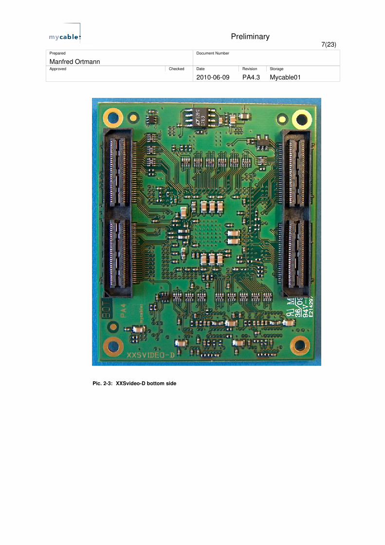
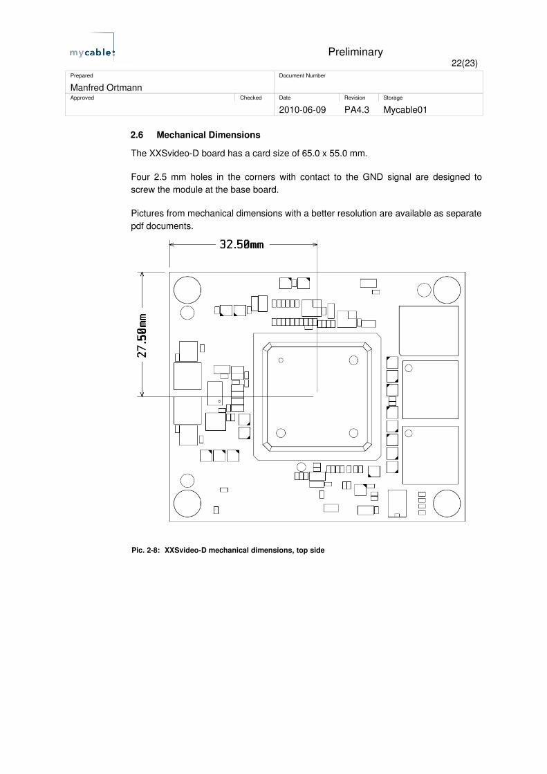
2.6 Mechanical Dimensions
The XXSvideoD board has a card size of 65.0 x 55.0 mm.
Four 2.5 mm holes in the corners with contact to the GND signal are designed to screw the module at the base board.
Pictures from mechanical dimensions with a better resolution are available as separate pdf documents.
Pic. 28: XXSvideoD mechanical dimensions, top side
Preliminary23(23)
Prepared Document Number
Manfred OrtmannApproved Checked Date Revision Storage
20100609 PA4.3 Mycable01
Pic. 29: XXSvideoD mechanical dimensions, bottom side