Embed Size (px)
Citation preview
AQA Physics A-level
Section 13: Electronics Notes
www.pmt.education

3.13.1 Discrete semiconductor devices Discrete components are made up of a single semiconductor device, while an integrated circuit is made up of several semiconductor devices which are interconnected on a single silicon chip or wafer. 3.13.1.1 - MOSFET (metal-oxide semiconducting field-effect transistor) Transistors are switches which contain no moving parts, so they switch between states through changes in the arrangement of semiconductor materials. They can also be used to regulate current and voltage. The MOSFET is the most commonly used type of transistor, due to its efficiency and versatility. In order to understand a MOSFET, you must understand the semiconductors which form it. Semiconductors allow limited movement of charge carriers, meaning that if the charge carriers are given a small amount of energy they can cross through the material, otherwise they cannot. For comparison, in conductors no energy is needed by the charge carriers in order to move through the material, whereas in insulators, a large amount of energy is required to allow charge carriers to move through the material. There are two possible types of charge carriers in semiconductors: ➔ Electrons - these can be removed from atoms using thermal energy. ➔ Holes - these are formed when an electron leaves an atom, and are not physical
particles, however they behave like positively charged particles, with a charge equal in magnitude to the charge on an electron. They act like particles because electrons can move into a hole, forming a hole elsewhere in the material (therefore the hole moves).
There are also two types of semiconductors, which depends on what type of charge carrier the material has an excess of:
● N-type - have an excess of conduction electrons. ● P-type - have an excess of holes.
If a p-type and an n-type material are placed close to each other (for example in a p-n junction), the conduction electrons on the n-type material closest to the p-type material are
www.pmt.education

attracted towards the holes and fill them. This causes a region at the edges closest to the meeting point of the materials to have no spare charge carriers, therefore it is called the depletion zone, which acts as an insulator, and so a large positive voltage must be supplied to the p-type material for electrons to cross into the p-type material and for the depletion zone to be removed. A MOSFET has 3 terminals:
1. Drain - where electrons leave, connected to the positive terminal. 2. Gate - a voltage here will turn the MOSFET on. 3. Source - the source of electrons, this is the negative terminal.
The current used in electronics is conventional current, therefore it flows from positive to negative (from drain to source). A MOSFET is formed using two p-n junctions. The diagram shows the structure of the MOSFET when an adequate voltage is supplied to the gate. When there is no voltage across the gate the n-channel doesn’t exist, this region is instead made up of a depletion zone, meaning that no current can flow. However, when a positive voltage is supplied to the gate, an electric field forms across the n-channel repelling holes and attracting electrons, and the size of the depletion zone decreases, allowing electrons to travel across the n-channel from the source to the drain. As the voltage across the gate increases, the width of the n-channel will increase until it reaches its maximum size, at this point the MOSFET is saturated, and the current can only be increased by increasing the supply voltage. If the voltage drops to zero, the n-channel will collapse. Due to the insulation between the gate and p-type material, the resistance between the gate and the other electrodes is extremely high, therefore a MOSFET will draw almost zero current from the circuit connected to the gate.
www.pmt.education

A MOSFET has several measurement parameters, which you need to be aware of: ● VDS - the voltage between the drain and the source. ● VGS - the voltage between the gate and the source . ● Vth - the threshold voltage, which is the minimum value of gate voltage (VGS) required
to form a conducting channel between the drain and source and allow current to flow. ● IDS - the current between the drain and source. ● IDSS - the small amount of current flowing between the drain and source when the gate
voltage (VGS) is zero. When the gate voltage (VGS) is below the threshold voltage (Vth), the MOSFET is off because there is no n-channel for electrons to move through, however a very small amount of current (IDSS) will still flow. As the gate voltage (VGS) increases above the threshold voltage (Vth), the MOSFET turns on because an n-channel begins to form. This channel allows electrons to pass through it, so IDS will increase slowly at first, then sharply. As gate voltage increases further the n-channel increases in width, allowing more electrons to pass through so IDS also increases until the n-channel reaches its maximum width. The above output characteristics can be shown on a graph of drain-source current (IDS) against drain-source voltage (VDS). A graph of drain-source current (IDS) against gate voltage (VDS) is used to show the input characteristics of a MOSFET. As you can see, once the gate voltage reaches the threshold voltage, IDS increases slowly at first, then sharply.
www.pmt.education

The operation of a MOSFET has 4 main regions: ➔ Cut-off region - VGS < Vth
Gate voltage is below threshold voltage so the MOSFET is turned off, so no current will flow and it acts as an open switch.
➔ Ohm’s law region - VGS > Vth
The MOSFET acts as a variable resistor (which varies with gate voltage) up until it becomes saturated.
➔ Saturation region - VGS > Vth
The MOSFET is fully on and the current cannot increase any further and the value of current will depend on the value of VGS.
➔ Breakdown region - VGS >> Vth
The gate voltage reaches the breakdown voltage, which causes a large current to flow into the transistor, destroying it.
A MOSFET can be used as a switch by varying the gate voltage supplied:
● When VGS = 0 V, the MOSFET is off and no current will flow. ● When VGS > Vth, the MOSFET is fully on (saturated) and so maximum current flows.
When using a MOSFET as a switch for an inductive component (one which can induce a current, e.g a solenoid), you must also connect connect a protection diode across the component. This is because turning the MOSFET off will cause a current to be induced, which oppose the motion which caused it (Lenz’s law). This may cause the MOSFET to become broken, so the protection diode is used as it will short-circuit the coil and protect the MOSFET. Due to the MOSFET’s high input resistance, electrostatic charge can build up at the gate, and cause the transistor to become damaged. To prevent this, a resistor can be connected between the gate and 0 V, so that charge has a region to flow off into. This resistance should be very high so that it does not draw much current from the input (gate). 3.13.1.2 - Zener diode A zener diode is a particular type of semiconductor diode, which: ➔ In the forward bias - will act like an ordinary diode, meaning that it will allow current to
flow easily in this direction once the voltage is greater than the threshold voltage. The threshold voltage is the minimum voltage required for a current to flow.
➔ In the reverse bias - unlike an ordinary diode, which is manufactured to have the highest breakdown voltage possible, a zener diode is manufactured to have a relatively low and specific breakdown voltage. The breakdown voltage of a diode is the minimum reverse voltage, which will cause a significant current to flow through the diode in the reverse bias. In an ordinary diode, reaching the breakdown voltage will cause it to become damaged, however this is not true for a zener diode due to its construction, meaning they can be used at their breakdown voltages.
www.pmt.education
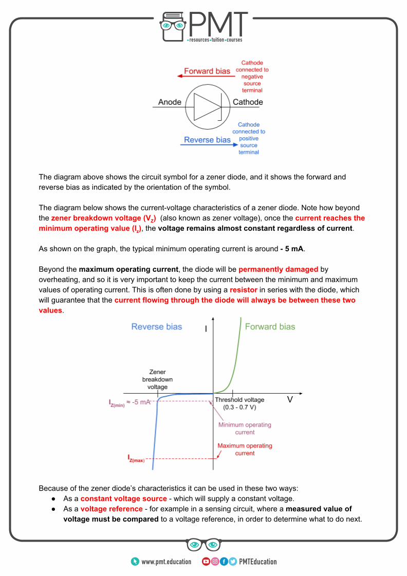
The diagram above shows the circuit symbol for a zener diode, and it shows the forward and reverse bias as indicated by the orientation of the symbol. The diagram below shows the current-voltage characteristics of a zener diode. Note how beyond the zener breakdown voltage (VZ) (also known as zener voltage), once the current reaches the minimum operating value (Iz), the voltage remains almost constant regardless of current. As shown on the graph, the typical minimum operating current is around - 5 mA. Beyond the maximum operating current, the diode will be permanently damaged by overheating, and so it is very important to keep the current between the minimum and maximum values of operating current. This is often done by using a resistor in series with the diode, which will guarantee that the current flowing through the diode will always be between these two values.
Because of the zener diode’s characteristics it can be used in these two ways:
● As a constant voltage source - which will supply a constant voltage. ● As a voltage reference - for example in a sensing circuit, where a measured value of
voltage must be compared to a voltage reference, in order to determine what to do next.
www.pmt.education

However, it can only be used in these ways given that:
➔ The input voltage is greater than the zener voltage of the diode (Vinput > VZ). ➔ The current is greater than or equal to about - 5 mA and is kept constant ➔ No current is drawn from the output of the circuit.
The value of R, from the diagram above can be calculated by using the (minimum) value of input voltage, zener voltage, and the minimum operating current of the diode. For example, a zener diode is used in a circuit connected to a speaker which requires a constant output of 4 V, and a maximum current of 100 mA. The input voltage is 10 V and the minimum operating current of the diode is 5 mA. Find the value of R required in this circuit.
The zener voltage across the diode must be 4 V so that the voltage across the speaker is also 4 V. Given this, find the voltage required across the resistor.
6 V01 − 4 =
The speaker requires a maximum current of 100 mA, while the diode requires a minimum current of 5 mA, meaning that the total current in the circuit will be 105 mA (assuming maximum load current). Given this information, and the voltage across the resistor calculated above, find the resistance of the resistor.
57 ΩR = IV = 6
105×10−3 =
www.pmt.education
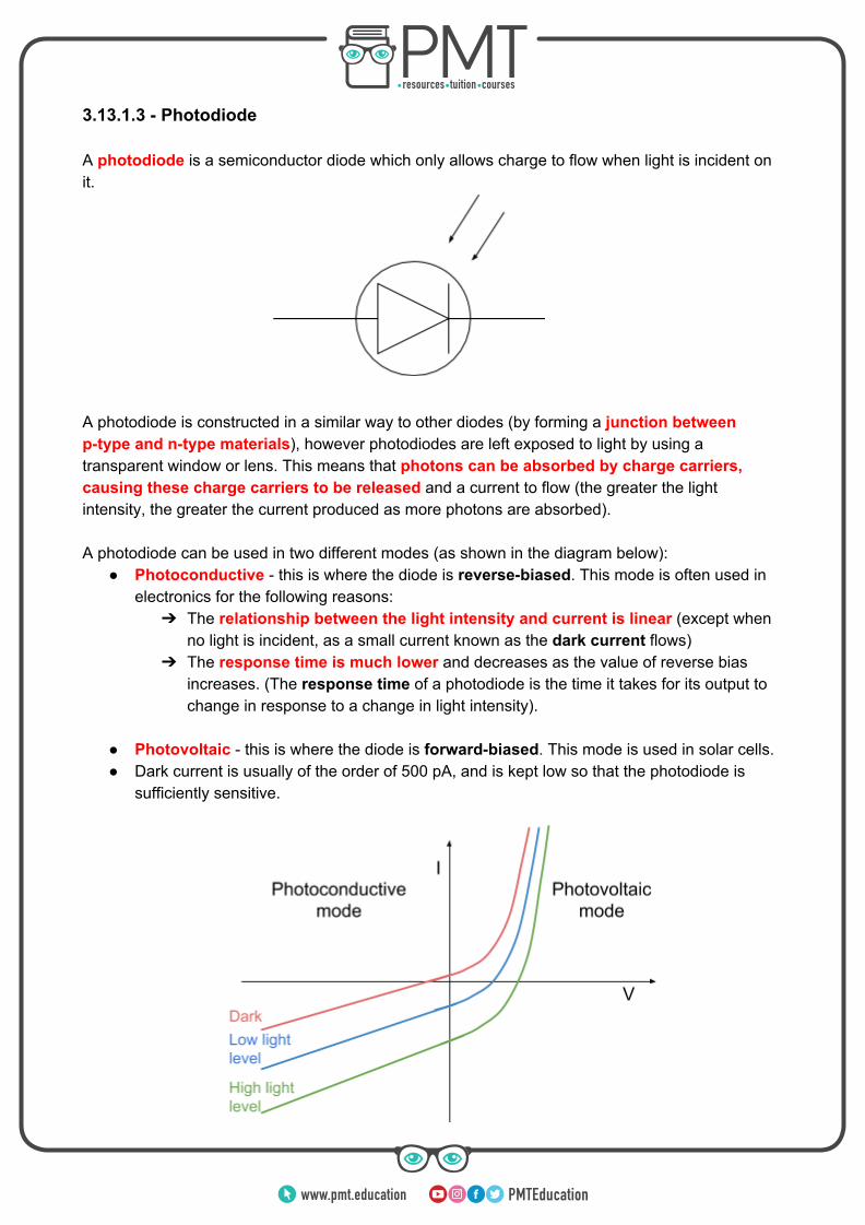
3.13.1.3 - Photodiode A photodiode is a semiconductor diode which only allows charge to flow when light is incident on it. A photodiode is constructed in a similar way to other diodes (by forming a junction between p-type and n-type materials), however photodiodes are left exposed to light by using a transparent window or lens. This means that photons can be absorbed by charge carriers, causing these charge carriers to be released and a current to flow (the greater the light intensity, the greater the current produced as more photons are absorbed). A photodiode can be used in two different modes (as shown in the diagram below):
● Photoconductive - this is where the diode is reverse-biased. This mode is often used in electronics for the following reasons: ➔ The relationship between the light intensity and current is linear (except when
no light is incident, as a small current known as the dark current flows) ➔ The response time is much lower and decreases as the value of reverse bias
increases. (The response time of a photodiode is the time it takes for its output to change in response to a change in light intensity).
● Photovoltaic - this is where the diode is forward-biased. This mode is used in solar cells. ● Dark current is usually of the order of 500 pA, and is kept low so that the photodiode is
sufficiently sensitive.
www.pmt.education

A photodiode has a different responsivity to different wavelengths of light, this is described by the diode’s spectral response. The responsivity (also known as sensitivity) is the ratio of the current generated to the power incident on the diode.
esponsivity/Sensitivity R = current generatedpower incident on diode
A diode’s spectral response depends on the way it is manufactured and can be represented by a spectral response curve. The spectral response curve below shows the relative responses of 3 photodiodes, S, M, and L. The spectral response of S peaks at around 450 nm, therefore it is most sensitive to light in this region. Note that photodiodes can be manufactured to have spectral responses in UV and infrared light, not just visible light (as shown below).
Image source: Vanessaezekowitz,CC BY 3.0, Image is edited through the addition of scales
Photodiodes used in photoconductive mode can be used as detectors in optical systems, for example:
● Smoke detectors - In certain smoke detectors, there is a source of pulsing infrared light and a photodiode, which is positioned so that no light is incident on it. The detector is also designed so that light from external sources cannot enter it. When smoke enters the detector, the infrared light is scattered and some is incident on the photodiode, which causes the diode to generate a current, which can be amplified to sound an alarm.
● Light detectors - Photodiodes are usually used as light detectors in optical fibre
communication systems due to being cheap to produce, small in size and being reliable. When light from the fibre is incident on the diode, a current is produced, which can be amplified and recorded.
A scintillator is a material which emits light photons when struck by particles or high energy photons. The energy of the light photons emitted by the scintillator is proportional to the energy
www.pmt.education

of the particles or high energy photons it absorbs. Scintillators and photodiodes can be used together to detect atomic particles:
1. A photodiode is bound to a scintillator material (e.g caesium iodide), so that when a particle collides with the material and it emits light photons, the photodiode can easily absorb them and produce an electric current, which can be amplified and recorded.
2. Using the recorded values of current, the energy of the particles can be calculated, and the number of light pulses can be counted meaning atomic particles can be detected.
In order to get maximum detection efficiency, the spectral response of the photodiode must be matched to the wavelengths of light produced by the scintillator. 3.13.1.4 - Hall effect sensor When a current-carrying semiconductor is placed in a magnetic field, a potential difference is produced perpendicular to the direction of current flow, this is known as the Hall effect. The voltage produced is proportional to the magnetic flux density of the field, and is called the Hall voltage (VH). Because of this, Hall sensors can be used to measure the detected magnetic flux density of a field by measuring the potential difference produced. Hall sensors can be used to monitor the orientation/angle change of an object. In order to do this, a magnet must be attached to the object so that there is a magnetic field for the Hall sensor to interact with.
www.pmt.education

As the object is rotated, the component of magnetic flux density detected by the hall sensor will change, so the Hall voltage produced will also change, meaning the orientation of an object can be monitored by measuring the output Hall voltage. The horizontal and vertical position of an object can be calculated in a similar way: ➔ As a magnet is moved across the face of a hall sensor maintaining a fixed gap, the Hall
voltage generated will change as the number of field lines passing through the sensor at a right-angle changes.
➔ The hall voltage is measured and can be related to the position of the magnet. By using the methods above, the attitude (orientation and position) of an object can be monitored. A tachometer is a device which measures the speed of rotation of an engine, or any other rotating component, by using a Hall effect sensor. A tachometer can be constructed by:
● Attaching a magnet to the rotating component - As the component rotates, the magnet moves past a stationary Hall sensor, which will produce a pulse of Hall voltage when the component passes it.
● Using a stationary magnet and attaching a toothed wheel made out of a ferrous material to the rotating component, between the sensor and the magnet - As the component rotates, the position of the wheel will affect the magnetic field strength and so will affect the Hall voltage produced by the Hall sensor.
www.pmt.education

In both types of tachometers, the output of the Hall sensor will be a pulsed signal, the frequency of which can be used to find the rotation speed of the component. The advantages of using a tachometer are:
1. They can measure very fast rotation speeds (over 100 kHz). 2. They do not make any contact which the shaft of the rotating object, so there are no
additional frictional forces applied. 3. They are small so can be used in confined spaces.
www.pmt.education

3.13.2 Analogue and digital signals 3.13.2.1 - Difference between analogue and digital signals Analogue signals are continuous and so can take any value. They used to represent “real-world” quantities, below are some examples of sensors and the analogue data they record:
● LDR/photodiode - light intensity ● Microphone - sound ● Hall effect sensor - magnetic field strength ● Thermistor - temperature ● pH probe - pH level ● Lambda sensor - oxygen level ● Flow sensor - pressure
It is important to note that not all of these sensors produce a signal voltage, for example the LDR and thermistor change resistance when they detect a change in light intensity or temperature (respectively). Therefore, additional circuitry is used to turn a resistance change into a voltage or current. Digital signals are discrete, meaning they can only take one of two values, either on/off or true/false. These on/off signals are represented using either a 1 or a 0. The value of the on/off states can vary depending on the circuit, however the off state is usually 0 V, while the on state is the supply voltage. The typical value of the on state for digital circuits is 5 V. Binary numbers (base-2) are used to represent digital signals because they use a combination of 1s and 0s to form numerical values (larger values require more bits to be represented). A bit is the basic unit of information used for the representation of digital signals in computing and digital communication, and can take one of two values, 1 or 0. A byte is a string of 8 bits, and represents a group of 8 digital signals. The position of bits in a binary number is significant because bits in different positions have different possible values, below is an example byte and its value in base-10.
www.pmt.education

27 (128) 26 (64) 25 (32) 24 (16) 23 (8) 22 (4) 21 (2) 20 (1)
1 0 0 0 1 1 0 1
10001101 (base-2) = 128 + 8 + 4 + 1 = 141 (base-10) You need to be aware of binary equivalent to the numbers 0 to 10:
Decimal number (base-10) Binary number (base-2)
0 0000
1 0001
2 0010
3 0011
4 0100
5 0101
6 0110
7 0111
8 1000
9 1001
10 1010
Analogue data which needs to be processed by a computer, usually needs to be converted into digital signals using an A-D converter (ADC). An ADC works in the following way:
1. The analogue signal is sampled at regular intervals. The size of the intervals is determined by the sampling rate.
2. These samples are converted into a binary number, which represents the analogue signal’s amplitude at the time the sample is taken. The amplitude is rounded to the nearest available discrete value.
3. This process is repeated for the whole piece of the analogue data and a sequence of numbers is produced, which represents the variation of amplitude (of the signal) over time.
www.pmt.education

This process is known as quantisation, as continuous values are assigned one of a number of discrete values. The quality of the conversion (how well an analogue signal is represented by a digital one) is dependent on the following parameters:
● Sampling rate - this is the number of samples taken per second As the sample rate increases, the quality of conversion increases, because the risk of missing out signal variations decreases. However, increasing the sampling rate means that the electronics used to do the conversion must become much more complex as the amount of data required increases. ➔ Generally, the minimum sampling rate is twice the frequency of the highest
recorded frequency in the analogue signal.
● Resolution - this is the smallest change in analogue signal which will cause a change in digital signal output, and is determined by the number of bits used to represent an analogue value. As the number of bits increases, the smallest change decreases (so resolution is increased). As the number of bits increases, the number of possible discrete values that can be assigned increases. The quality of conversion increases because this causes the approximation error to decrease. The number of bits, n, allows for 2n possible values. For example, 3 bits allows (23 =) 8 possible values to be assigned. So if you use 3 bits and the maximum recorded (analogue) value is 10 V, the resolution is 10/8 = 1.25 V.
www.pmt.education

➔ Generally, the minimum resolution needed to provide an adequate conversion is 8 bits.
2-bit resolution 3-bit resolution
Image source (left): Hyacinth,CC BY-SA 3.0 Image source (right): Hyacinth,CC BY-SA 3.0 The advantages of digital sampling are:
● Digital signals are much easier to process than analogue signals. ● Digital signals are less likely to be affected by noise, meaning they can be used when
transmitting signals over long distances. Even if they are affected by noise, it is relatively easy to recover the original signal.
● Digital signals can be transmitted using optical fibres. ● Digital signals can be encoded, which means they can be made to only be readable by the
person who is intended to receive them. This also means that you can send many digital signals using the same optical fibre, as they can be extracted and separated easily.
The disadvantages of digital sampling are:
● Digital signals provide less exact information in comparison to analogue signals as values of amplitude are rounded and so there is an approximation error.
● Generally, the systems for transmitting digital signals are more complex and so require a greater bandwidth than an analogue signal. The bandwidth is the range of frequencies that are used for transmitting a signal.
When being transferred, signals will be affected by a certain level of noise. Noise causes random variations in the signal, for example the noise in a reading of voltage (over time) will be caused by random voltage fluctuations caused by interference from the electronic system and external sources. Noise adds random information to a signal. Analogue signals may require amplification, however this will also amplify the noise affecting the signal. If amplified too many times, the original signal may become undecipherable. Digital signals will also experience noise, however because digital signals are formed of two distinct states (on/off), they are less affected. This is because the states are still recognisable
www.pmt.education

in a digital signal, whereas in an analogue signal the shape of the signal contains the signal’s information and this is what is affected by noise.
Image source: Krupsi 1999,CC BY-SA 4.0
If a signal has a high enough level of noise, it will become very hard to distinguish the original signal. There are two methods for reducing the effect of noise on a system:
● Repeaters - These will amplify the signal, reducing the amount of attenuation. Attenuation is where part of the signal’s energy is absorbed, reducing the amplitude of the signal, making it harder for the original signal to be distinguished. As noted above, amplification will also amplify noise.
● Regenerators - These regenerate a noisy signal. These work by using a switching circuit, which turns on when the input signal is above the upper switching threshold and turns off when the signal is below the lower switching threshold. A switching threshold is a particular voltage which when reached will cause the circuit to either turn on/off as described above.
The process of analogue-to-digital signal conversion is known as pulse code modulation. There are 3 stages of pulse code modulation: ➔ Sampling - where the signal is measured at regular intervals at a constant sampling
rate.
www.pmt.education

➔ Quantisation - where the measured (continuous) values are assigned a discrete value by rounding (which introduces an approximation error).
➔ Encoding - where the discrete values are represented by a binary number, which has a length n, dependent on the resolution of the conversion.
ADC will produce a parallel output as the n number of bits produced will be output simultaneously. Data is usually transmitted by using a single transmission path, therefore in pulse code modulation, a parallel-to-serial converter can be used. This device will convert the parallel data into serial data, which is formed of a single stream.
www.pmt.education
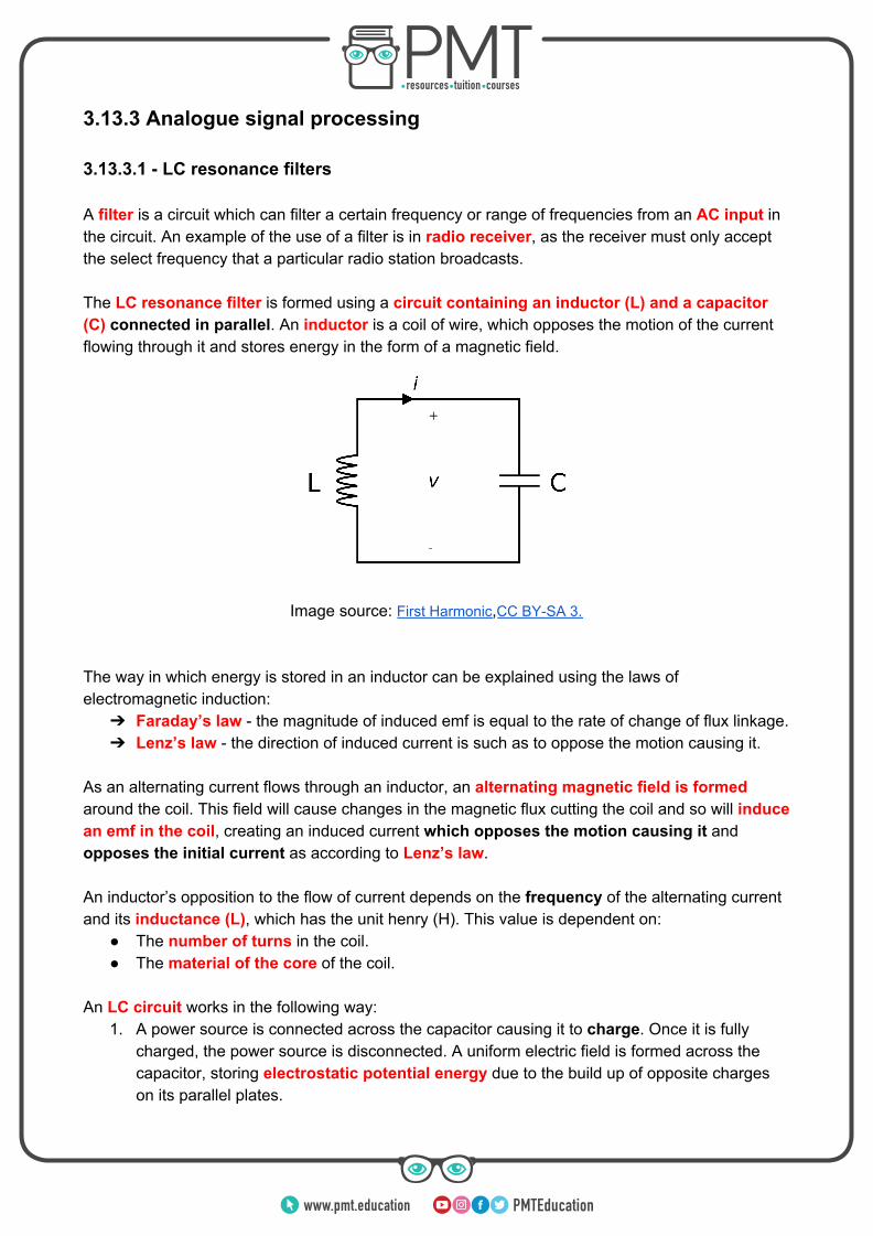
3.13.3 Analogue signal processing 3.13.3.1 - LC resonance filters A filter is a circuit which can filter a certain frequency or range of frequencies from an AC input in the circuit. An example of the use of a filter is in radio receiver, as the receiver must only accept the select frequency that a particular radio station broadcasts. The LC resonance filter is formed using a circuit containing an inductor (L) and a capacitor (C) connected in parallel. An inductor is a coil of wire, which opposes the motion of the current flowing through it and stores energy in the form of a magnetic field.
Image source: First Harmonic,CC BY-SA 3. The way in which energy is stored in an inductor can be explained using the laws of electromagnetic induction: ➔ Faraday’s law - the magnitude of induced emf is equal to the rate of change of flux linkage. ➔ Lenz’s law - the direction of induced current is such as to oppose the motion causing it.
As an alternating current flows through an inductor, an alternating magnetic field is formed around the coil. This field will cause changes in the magnetic flux cutting the coil and so will induce an emf in the coil, creating an induced current which opposes the motion causing it and opposes the initial current as according to Lenz’s law. An inductor’s opposition to the flow of current depends on the frequency of the alternating current and its inductance (L), which has the unit henry (H). This value is dependent on:
● The number of turns in the coil. ● The material of the core of the coil.
An LC circuit works in the following way:
1. A power source is connected across the capacitor causing it to charge. Once it is fully charged, the power source is disconnected. A uniform electric field is formed across the capacitor, storing electrostatic potential energy due to the build up of opposite charges on its parallel plates.
www.pmt.education

2. The capacitor is connected in parallel to the inductor, so charge begins to flow from the capacitor to the inductor. As the capacitor loses charge, the electrostatic potential energy decreases, while the energy stored in the magnetic field in the inductor increases.
3. Once the capacitor is completely discharged, no more current flows. This means there is no longer a rate of change of flux in the inductor, so the magnetic field subsides causing the induction of an emf. The induced current is in the opposite direction to the initial current due to Lenz’s law.
4. The current flows from the inductor to the capacitor causing it to charge up in the opposite direction (so with opposite polarity). The energy stored by the magnetic field is transferred to electrostatic potential energy in the capacitor.
5. The capacitor charges fully to its initial voltage and the above cycle (from step 2 onwards) will repeat. And so the circuit “oscillates”.
The above process is analogous to a (horizontal) mass-spring system, where mass is the inductance and the spring is the capacitance, for example: ➔ In part one (above), the capacitor is fully charged by an external power source, this is
analogous to an external force pulling the spring to its maximum displacement. In the LC circuit, all the energy is stored as electrostatic potential energy, while in the mass-spring system, all the energy is stored as elastic potential energy.
➔ In part three, the capacitor is completely discharged while the inductor is fully charged which is analogous to a spring reaching a displacement of zero while the mass is travelling at maximum velocity. In the LC circuit, all the energy is now stored in the magnetic field formed by the inductor, while in the mass-spring system, all the energy is now stored as kinetic energy of the mass.
As in any oscillating system, the system will eventually stop oscillating as energy is lost due to resistive forces, for example in the mass-spring system, the resistive force is air resistance, while in an LC circuit energy is dissipated due to resistance in the circuit. And so to prevent the oscillations from decreasing in amplitude and stopping, an external driving force is required. If the frequency of the driving force is near or equal to the natural frequency of a system, resonance occurs. Resonance is where the amplitude of oscillations of a system drastically increase due to gaining an increased amount of energy from the driving force.
www.pmt.education

The driving force in an LC circuit is a source of emf with an alternating frequency, the charge will oscillate between the inductor and capacitor at the frequency of the source. Therefore, if the frequency of the emf source is equal to the natural frequency of the LC circuit, resonance will occur. You can calculate the resonant frequency (f0) (also known as the natural frequency) of an LC circuit using the following equation:
f 0 = 12π√LC
Where L is the inductance and C is the capacitance. The frequency calculated will be given in hertz (Hz) if the inductance is in henry (H) and capacitance is in farad (F). Energy response curves of LC circuits show the variation of energy stored in the circuit against frequency of the driving force, below is an example: As you can see, the energy stored by the circuit is at its maximum value when the frequency is equal to the resonant frequency. If the inductance or capacitance of the circuit is adjusted, the resonant frequency would change and so the peak of the graph will shift accordingly. The shape of a voltage-frequency graph is the same as above. The effect of an increase in electrical resistance in an LC circuit, is analogous to an increase in the amount of damping experienced by a mass-spring system. Therefore, as the degree of
www.pmt.education

damping/electrical resistance increases, the resonant frequency decreases (shifts to left on a graph), the maximum amplitude decreases and the peak of maximum amplitude becomes wider, these effects are shown in the graph below: (ζ is the damping ratio, ζ = 1 represents critical damping)
Image source: Geek3,CC BY 3.0
The bandwidth (fB) of the filter is the range of frequencies where the energy is greater than or equal to 50% of the maximum energy. When looking at a graph of voltage gain (Vout/ Vin) against frequency, you can also find the bandwidth however the range is found where the voltage is equal to or 0.71 of the peak voltage.1
√2
The width of the resonant peak for an LC filter is important in determining the application of the filter. The Q factor (Q) (quality factor) can be used to measure the sharpness of the resonant peak:
Q = f0fB
Where f0 is the resonant frequency and fB is the bandwidth.
www.pmt.education

Using a filter with a small Q-factor will lead to: ● A broader bandwidth ● More noise detected ● Lower ability to select a particular frequency, and so in a radio tuner there is more
susceptibility to multiple stations being heard at once ● High rate of energy losses
Using a filter with a high Q-factor will lead to:
● A narrow bandwidth ● Less noise detected ● Better ability to select a particular frequency ● Low rate of energy losses
3.13.3.2 - The ideal operational amplifier An amplifier is a device which increases the signal strength of an analogue signal input. The diagram on the right shows the output voltage (VO) of an amplifier and its input voltage (Vi) for comparison. An operational amplifier (op-amp) is an important system building block, which can be configured in many different ways in order to cause amplification of signals for different applications. Below is the circuit symbol for an op-amp. Note that the inverting input (V-) and non-inverting input (V+) can sometimes swap positions to reduce clutter in circuit diagrams, therefore it is always important to check which input is which.
Image source: User: Omegatron,CC BY-SA 3.0
Amplification can be measured using a value called gain (A), which is the ratio of output voltage and input voltage as shown below:
A = input voltageoutput voltage = V in
V out
www.pmt.education

There are two types of gain in an op-amp, these are:
● Open-loop gain (AOL) - this is where there is no feedback in the circuit, so no signals are fed from output back to input.
● Closed-loop gain (ACL) - this is where part of the output is fed back into the input. An operational amplifier will amplify the voltage between the two inputs, as shown in the equation for the output of an op-amp below, this is known as its open-loop transfer function:
(V ) V out = AOL + − V − Where AOL is the open-loop gain, V+ is the non-inverting input and V- is the inverting input.
An ideal operational amplifier is assumed to have the following features: ➔ Infinite open-loop gain (AOL) - this means that the op-amp can produce any finite gain
required by the system in a closed-loop circuit. In an open-loop circuit, this feature is used to compare voltages as a comparator circuit (explained in more detail below).
➔ Infinite input resistance (between V+ and V- inputs) - meaning that inputs will draw no current from the signal sources connected to them.
➔ Infinite bandwidth - which means that the op-amp can operate at any input frequency. ➔ Zero output resistance - meaning that the output current of the op-amp is unaffected.
An operational amplifier cannot generate an output voltage which is greater than its supply voltage. If such an input is used which attempts to produce an output greater than Vs+ or less than Vs-, the output voltage will stay at Vs+ or Vs- despite any further increase in input voltage. This is called saturation, as even as the difference in input voltages increases, output voltage remains constant. Below is a graph which shows the variation in output voltage, against the change in the two input voltages.
Using the equation , you can see that the gradient of the linear region is AOL.(V ) V out = AOL + − V − As mentioned above, an operation amplifier in an open-loop circuit can be used to compare its two input voltages in a comparator circuit.
www.pmt.education

The table below summarises the possible voltage outputs of the example comparator circuit below it.
Vout Explanation
V1 > V2 +10 V The op-amp tries to output a voltage defined by the equation
however, as AOL(V ) V out = AOL + − V − is infinite, this is not possible. So the amplifier is saturated and will output either +10 V or -10 V depending on
which input is larger.
V1 < V2 -10 V
V1 = V2 0 V / undefined
The equation for Vout states that in this case Vout should be zero. In reality though, this can never occur and so the output in undefined.
Comparators are usually used in sensor circuits, for example a circuit which detects when the temperature in a room drops below a certain level and causes a heater to turn on as a result. An example circuit is shown below:
A PTC (positive temperature coefficient) thermistor is used in the circuit, because as
www.pmt.education

its temperature decreases, the resistance of the thermistor decreases. The potential divider formed of the thermistor and R1 will produce a varying voltage, which is used as the non-inverting (V+) input of the op-amp. The potential divider formed by the variable resistor and R2 will produce a constant voltage (which can be adjusted using the variable resistor), which is used as the inverting input (V-). ➔ When the temperature of the thermistor is low, its resistance will also be low, therefore
the voltage across R1 will be large, and so V+ will also be large. Given that V+ is larger than the voltage across the variable resistor, the output to the heater will be +120 V so it will be turned on.
➔ When the temperature of the thermistor is high, its resistance will also be high, therefore the voltage across R1 will be small, and so V+ will also be small. Given that V+ is smaller than the voltage across the variable resistor, the output to the heater will be 0 V so it will be turned off.
The resistance of the variable resistor can be adjusted, which also adjusts the voltage across it and so the inverting input (V-), in order to adjust the temperature at which the heater will be switched on.
www.pmt.education

3.13.4 Operational amplifier in: 3.13.4.1 - Inverting amplifier configuration In an inverting amplifier configuration, the output voltage from the operational amplifier is fed back into the inverting input of the op-amp, forming a closed-loop circuit with negative feedback. Due to this, the gain of the op-amp can be adjusted to much lower values. An example inverting amplifier configuration is shown on the right. Note that the power supply connections are not shown, however unless otherwise noted, they are assumed to be present. Using virtual earth analysis, and the assumptions noted below, we can derive the transfer function (voltage output equation) for this type of circuit. Assumptions:
● The op-amp is ideal (requirements for this are noted above). ● The op-amp in operating in its linear region and so is not saturated, .V|| out
|| < V S
By looking at the inverting amplifier configuration above, you can see that the non-inverting input voltage is 0 V (as it is connected to the ground). And as the op-amp is ideal, it has infinite open-loop gain (AOL). Using these pieces of information, we can rewrite the open-loop transfer function as shown:
(V ) V out = AOL + − V − (0 ) V out = ∞ × − V −
VV − = ∞−V out ⇒ V − = 0
This equation shows us that the voltage at the inverting input is virtually zero, as it is such a small value (because it is divided by infinite open-loop gain) it can be regarded as zero. This point in the circuit is known as a virtual earth, as even though it is not connected to earth, it (virtually) has a value of 0 V. The location of the virtual earth is shown on the circuit on the right using a red cross.
www.pmt.education

The derivation below uses virtual earth analysis as the virtual earth gives a steady reference potential which is used to analyse the circuit:
1. As the op-amp is ideal, its input resistance is infinite so no current will be drawn into the inverting input, meaning IX = 0 A. Using Kirchoff’s current law, which states that the total current flowing into a junction is equal to the current flowing out of that junction, we can see that current passing through Rin (IR1) is equal to the current passing through Rf (IRf), so IR1 = IRf .
2. Using V=IR, you can find the voltage across Rin (VR1) and Rf (VRf):
V R1 = IR1 × R1 V Rf = IRf × Rf
3. As IR1 = IRf, you can rearrange the above equations for current, equate them, then
rearrange the final equation for VRf as shown below:
IR1 = R1
V R1 IRf = Rf
V Rf
R1
V R1 = Rf
V Rf
V Rf = R1
V R1 × Rf 4. Using Kirchoff’s voltage law, which states that the sum of all the voltages in closed loop
is equal to zero, we can find the value of Vout. The only two voltages involved in the loop containing the op-amp and the output are VRf and Vout, so…
V Rf + V out = 0 V out = − V Rf
5. Using the equations defined in the last two steps, we can form the transfer function.
)V out = − ( R1
V R1 × Rf
V R1
V out = −RfR1
VR1 can be rewritten as Vin and R1 can be rewritten as Rin to get the following equation:
V in
V out = −Rf
Rin
www.pmt.education

Below is a graph which shows the output voltage (VO) of an inverting amplifier and its input voltage (Vi) for comparison. As you can see, the input is not only amplified but its polarity is inverted giving this formation its name. An advantage of the inverting amplifier configuration is that the input signals experience lower levels of distortion in comparison to non-inverting amplifiers.
3.13.4.2 - Non-inverting amplifier configuration A non-inverting amplifier configuration does not affect the polarity of the signal, so is useful if a signal must be amplified and keep its original polarity. In this configuration, the output voltage from the operational amplifier is fed back into the non-inverting input of the op-amp, forming a closed-loop circuit with negative feedback. Below is an example non-inverting amplifier configuration.
www.pmt.education

The transfer function of a non-inverting amplifier configuration is given below:
V in
V out = 1 +Rf
R1
(you do not need to know how to derive this result) It is important to note that the gain can never be lower than 1. An advantage of this circuit over the inverting amplifier circuit is that the input signal is connected directly to the op-amp, meaning the entire circuit draws no current due to the op-amp’s infinite input resistance. Whereas the inverting amplifier circuit will draw a current across Rf. If the resistance of Rf becomes 0 and/or the resistance of R1 becomes infinite the following circuit is formed:
The above circuit is known as a unity gain buffer (or unity gain amplifier) because the op-amp has a gain of 1 so no amplification occurs. These types of circuits are used as an interface between a signal source and device with a low input resistance, which draws no or very little current. Because of the op-amp’s infinite input resistance, this buffer will draw very little current while still outputting the same input signal, not disturbing the original circuit.
www.pmt.education

3.13.4.3 - Summing amplifier configuration A summing amplifier configuration allows several signals to be connected in an inverting amplifier and amplified independently. The virtual earth in an inverting amplifier allows the signals to be connected without interference. Below is an example summing amplifier configuration.
The transfer function of a summing amplifier configuration is given below:
( ..)V out = − Rf R1
V 1 + R2
V 2 + R3
V 3 + . This type of amplifier is most commonly used as an audio mixer, where different audio inputs can be merged and their individual levels adjusted. A difference amplifier configuration allows the difference between two signals to be found (and subtracted). Below is an example difference amplifier configuration.
www.pmt.education

Usually the gain for the two inputs is equal, therefore the resistances R1 and R2 are made equal, and Rg and RF are also made equal. In this case, the transfer function of a difference amplifier configuration is given below:
V )V out = ( + − V −Rf
R1
This type of amplifier is often used in noise cancellation, below are two examples: ➔ Balanced microphone -
Microphone leads can pick up interference, especially the 50 Hz signal output by mains electricity. It would not be ideal to filter out any signal at 50 Hz because part of the original signal would be lost, therefore a difference amplifier is used. The original signal, and an inverted signal are input into the amplifier, and subtracted from one another causing the interference to be cancelled out.
➔ ECG amplifier - The electrocardiogram (ECG) measures the change in potential difference produced by the heart over time by attaching several electrodes to the body. The leads connecting to the ECG and the human body can pick up interference, again mainly the 50 Hz signal output by mains electricity. Again, this interference can be reduced through the use of a difference amplifier, by attaching an additional electrode in a place where mostly only interference is picked up (e.g. on the patient’s ankle), and so this interference can be removed.
3.13.4.4 - Real operational amplifiers In reality operational amplifiers are not ideal, though there are many different types of op-amps which have characteristics optimised for certain applications. The table below shows a comparison between a typical and ideal op-amp, noting that the real values will vary for different op-amps.
Ideal Real
Open-loop gain (AOL) Infinite 106
Input resistance (Rin) Infinite - draws no current 1012
Output resistance (Rout) Zero 100 Ω
Output voltage (Vout) − V S ≤ V out ≤ + V S , − V S < V out < + V S= 0 V out /
Bandwidth Infinite - can operate at any input frequency
Open-loop - Around 15 Hz Closed-loop - Around 2.5 MHz
It is also important to note that real op-amps are affected by the temperature of the environment around them.
www.pmt.education

The open-loop gain of a real op-amp is not infinite, however it is still very high, so the assumption it is infinite holds well during analysis. The input resistance of a real op-amp is very high, however it is not infinite, meaning a very small current (of the magnitude nA) is drawn. The output resistance of a real op-amp is very high, which means that there is a limit on the current that can be delivered by a real op-amp. It is important to note that the output resistance is reduced when the op-amp is used in a circuit with negative feedback. When the inverting and non-inverting terminals are the same or both grounded, an ideal op-amp would output a value of 0 V, however a real op-amp will output a small voltage called the off-set voltage. This value must be cancelled out in many applications to allow proper operation; this is done by connecting the op-amp to an external voltage divider circuit (labelled offset null in diagram below). Also, a real op-amp cannot output the exact values of the positive or negative supply voltage due to resistance in the circuitry.
The diagram below shows the pin connections for one type of op-amp.
Image source: TedPavlic,CC BY-SA 3.0
The bandwidth, which is the range of frequencies at which the op-amp operates is very small in open-loop circuits due to its high gain. What is usually quoted on data sheets is the closed-loop bandwidth, where a unity gain amplifier circuit is used, as this allows for a larger bandwidth though gain is decreased. A frequency response curve shows how the voltage gain of an op-amp varies with the frequency of the input signal. Below is an example of a frequency response curve for an open-loop circuit. Frequency response curves may have a logarithmic scale due to the large values of gain and frequency.
www.pmt.education

The break frequency is the frequency at which the gain begins to change. As illustrated in the diagram, you can find this frequency by using straight-line approximations of the upper and lower part of the curve and finding where the straight lines intersect. If the x-axis of the graph starts at 0, the break frequency will also give you the value of bandwidth. This frequency response curve shows that if this op-amp was used as a comparator in an open-loop circuit, its performance will decrease beyond the break frequency, which limits its use. Below is a frequency response curve for the same op-amp but in a closed loop circuit.
As you can see, when the op-amp is used in a closed-loop circuit the break frequency increases significantly.
www.pmt.education

As seen in both frequency response curves, beyond the break frequency, the curve approximates a straight line. This means that the relationship between voltage gain and bandwidth is linear, meaning that the product of voltage gain and bandwidth must be constant for a given op-amp. The relationship defined above can be used to predict the bandwidth of a circuit and is summarised below:
ain bandwidth constant g × =
www.pmt.education

3.13.5 Digital signal processing 3.13.5.1 - Combinational logic Logic gates are electronic switching circuits, which give different outputs depending on their input. The output of a logic gate depends on the type of gate used and the input into the gate which can be one of the following:
● On - represented by a 1, this signifies that a current is present ● Off - represented by a 0, this signifies the absence of a current
Logic gates are used in many electronic systems, for example in the processor of a computer, where they process digital information. The use of several logic gates to form a desired outcome (depending on what is input into the system), is called combinational logic. Truth tables are used to show all the possible inputs into a logic gate and their outcomes, which make them useful for analysing simple combinational logic circuits to see how they function. When forming truth tables, you should list all the possible inputs in ascending numerical order (in binary) to make sure you have included all possibilities. Also, it is important to note that the number of possible input combinations is 2n where n is the number of inputs, for example a circuit with 4 inputs will have (24 =) 16 possible input combinations. There are 6 types of logic gates which you need to know about. The first three are the most basic logic gates, from which the rest are formed. Below are their circuit symbols and truth tables: ➔ AND gate - the output of this gate is 1 if both its inputs are 1, otherwise its output is 0
A B Out
0 0 0
0 1 0
1 0 0
1 1 1
➔ OR gate - the output of this gate is 1 if either or both inputs are 1, otherwise its output is 0
www.pmt.education
A B Out
0 0 0
0 1 1
1 0 1
1 1 1
Image source: Chris-martin,CC BY-SA 3.0
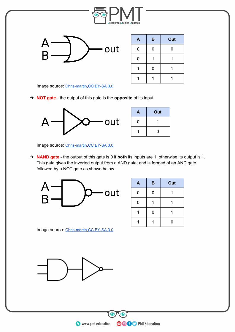
➔ NOT gate - the output of this gate is the opposite of its input
A Out
0 1
1 0
Image source: Chris-martin,CC BY-SA 3.0
➔ NAND gate - the output of this gate is 0 if both its inputs are 1, otherwise its output is 1. This gate gives the inverted output from a AND gate, and is formed of an AND gate followed by a NOT gate as shown below.
A B Out
0 0 1
0 1 1
1 0 1
1 1 0
Image source: Chris-martin,CC BY-SA 3.0
www.pmt.education

➔ NOR gate - the output of this gate is 0 if either or both inputs are 1, otherwise its output is 1. This gate gives the inverted output from an OR gate, and is formed of an OR gate followed by a NOT gate as shown below.
A B Out
0 0 1
0 1 0
1 0 0
1 1 0
Image source: Chris-martin,CC BY-SA 3.0
➔ EOR gate - this gate is known as the exclusive OR (EOR/XOR) gate. It gives an output of 1 only if one of its inputs is 1 but not both, otherwise its output is zero. This gate is sometimes called a digital comparator as it gives an output of 1 when its inputs are different. One of the possible formations of an EOR gate from AND, NOT and OR gates is shown below.
A B Out
0 0 0
0 1 1
1 0 1
1 1 0
Image source: Chris-martin,CC BY-SA 3.0
www.pmt.education

Boolean algebra allows the formation of mathematical expressions to describe logic circuits, it can also be used to draw and optimise logic circuits. Below are three relationships between signals (which are our variables) and how they are written in Boolean algebra:
A and B = A · B A or B = A + B
Not A = A The following rules allow the above functions to be combined with other variables:
1. The associative law - B C) A ) A · ( · = ( · B · C B C) A ) A + ( + = ( + B + C
2. The commutative law - A · B = B · A A + B = B + A
3. The distributive law - B ) A ) A ) A · ( + C = ( · B + ( · C B ) A ) A ) A + ( · C = ( + B · ( + C
Along with the above laws, there are several simplifications in Boolean algebra which you must be able to understand. These simplifications can be easily understood by drawing the appropriate logic gate and truth table. For example, one of these simplifications is : A and A gives A. From first glance, it is not A · A = A easy to spot why this is true, however if you think of the appropriate logic gate, which in this case is the AND gate and draw a truth table you can see this property is true.
A A A・A
0 0 0
1 1 1
Another example simplification is A + A = 1
A Ā A + Ā
0 1 1
1 0 1
Image source: Chris-martin,CC BY-SA 3.0, Inputs and output are edited
www.pmt.education
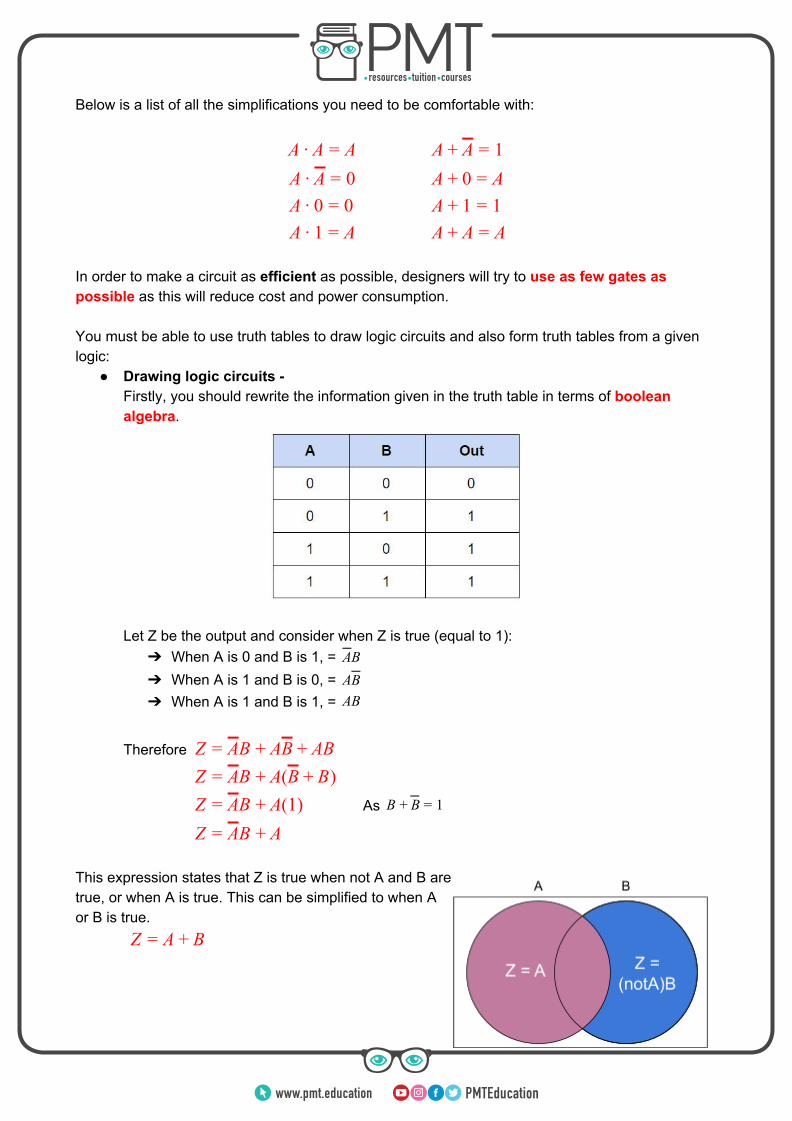
Below is a list of all the simplifications you need to be comfortable with:
A · A = A A + A = 1 A · A = 0 A + 0 = A A · 0 = 0 A + 1 = 1 A · 1 = A A + A = A
In order to make a circuit as efficient as possible, designers will try to use as few gates as possible as this will reduce cost and power consumption. You must be able to use truth tables to draw logic circuits and also form truth tables from a given logic:
● Drawing logic circuits - Firstly, you should rewrite the information given in the truth table in terms of boolean algebra. Let Z be the output and consider when Z is true (equal to 1): ➔ When A is 0 and B is 1, = BA ➔ When A is 1 and B is 0, = BA ➔ When A is 1 and B is 1, = B A
Therefore B B B Z = A + A + A B (B ) Z = A + A + B B (1) Z = A + A As B + B = 1
B Z = A + A
This expression states that Z is true when not A and B are true, or when A is true. This can be simplified to when A or B is true.
Z = A + B
www.pmt.education

www.pmt.education

Therefore, a single logic gate could be used to draw this logic circuit, the OR gate:
Image source: Chris-martin,CC BY-SA 3.0
The method described above involved simplification, however you do not have to simplify your Boolean expression before you draw you logic circuit. For example, given the following truth table and Boolean expression:
A B A B A · B A · B Z
0 0 1 1 0 0 0
0 1 1 0 1 0 1
1 0 0 1 0 1 1
1 1 0 0 0 0 0
A ) A ) Z = ( · B + ( · B You can identify the type and number of logic gates required to form the logic circuit from the above expression. In this example AND, NOT and OR gates are used: ➔ AND - there are two AND gates, ( ) and ( )A · B A · B ➔ NOT - there are two NOT gates, ( ) and ( )A B ➔ OR - there is one OR gate, ( )A ) A )( · B + ( · B
Now that you know how many of each gate you must use (and roughly where), you can form the logic circuit for this truth table.
www.pmt.education

● Forming truth tables -
Firstly, you should label intermediate signals within the circuit. One convention is to label input signals by using letters of the alphabet working from A onwards, and to label outputs from Z backwards. Below is an example logic circuit which is already labelled.
Image source: P Astbury,CC BY 4.0, Output label added
Then, draw a truth table containing all the possible primary inputs noting that the number of possible input combinations is 2n where n is the number of inputs. In the above example there are 3 inputs so there are (23 =) 8 possible combinations.
As noted before, you should list all the possible inputs in ascending numerical order to make sure you have included all possibilities.
A B C D E Z
0 0 0
0 0 1
0 1 0
0 1 1
1 0 0
1 0 1
1 1 0
1 1 1
www.pmt.education
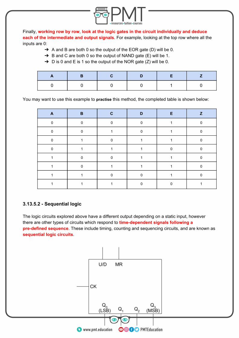
Finally, working row by row, look at the logic gates in the circuit individually and deduce each of the intermediate and output signals. For example, looking at the top row where all the inputs are 0:
➔ A and B are both 0 so the output of the EOR gate (D) will be 0. ➔ B and C are both 0 so the output of NAND gate (E) will be 1. ➔ D is 0 and E is 1 so the output of the NOR gate (Z) will be 0.
A B C D E Z
0 0 0 0 1 0
You may want to use this example to practise this method, the completed table is shown below:
A B C D E Z
0 0 0 0 1 0
0 0 1 0 1 0
0 1 0 1 1 0
0 1 1 1 0 0
1 0 0 1 1 0
1 0 1 1 1 0
1 1 0 0 1 0
1 1 1 0 0 1
3.13.5.2 - Sequential logic The logic circuits explored above have a different output depending on a static input, however there are other types of circuits which respond to time-dependent signals following a pre-defined sequence. These include timing, counting and sequencing circuits, and are known as sequential logic circuits.
www.pmt.education

Counting circuits are used in many systems and always count in binary, however their output can be converted to other forms. To the right is a circuit block for a binary counter, with its inputs on the top and left and its outputs on the right:
● CK - this is the clock input, which inputs pulses which are counted by the circuit. ● U/D - this is the up/down input which allows you to change whether the circuit counts up or
down. When the input is 1 it counts up, otherwise it counts down (this may be labelled as ).U /D
● MR - this is the master reset input. When its input is 1, all the counter outputs (Q0 to QN) reset and become 0.
● Q0 to QN - these are counter outputs and are used to output the value of the counter. ● Q0 - this is the least significant bit as it will change most frequently. This is due to the fact
it is the closest to the clock input. Q0 will always represent a difference of 1. ● QN - this is the most significant bit as it will change least frequently. This is due to the fact
it is furthest away from the clock input. The value QN depends on the number of bits in the counter. The counter shown in the diagram is a 4-bit counter so its QN is Q3, which will represent a value of 8.
A timing diagram is used to show the behaviour of a binary counter as its input signals change with time.
Image source: geeksforgeeks,CC BY-SA 4.0, Clock pulse scale is edited
www.pmt.education

As you can see from the diagram: ➔ The states of the counter outputs only change when the clock changes from 0 to 1, this is
known as the rising edge. Therefore this countered is said to be rising-edge triggered. ➔ When the counter reaches 0000, on the 16th clock pulse, the counter automatically resets.
An N-bit binary counter can only count up to 2N - 1, so in this case after (24 - 1 =) 15 pulses, the counter will reset.
➔ The pulse rate, which is the frequency of output pulses, is less than half of the clock’s frequency. Q0 has half the frequency of the clock, while Q1 has half the frequency of Q2, and Q3 has half the frequency of Q2. This is useful as the counter can be used as a frequency divider. For example, a usual digital watch produced pulses at 32768 Hz, this can be divided down to lower frequencies by a counter in order to count hours, minutes and seconds.
Another type of counting circuit is the modulo-n counter which counts up to a certain number before resetting to zero. Unlike in a binary counter, this final value does not have to be a power of 2. This type of counter is formed from a binary counter connected to logic gates, which cause the input to MR to become 1 when the counter reaches the chosen final value, causing it to be reset. Below is a diagram of a modulo-11 counter, which will count to 10 before resetting to zero. As you can see, once Q1 and Q3 become 1, and the output of the counter is (1010 =) 10, the AND gate gives an output of 1 to the master reset input, causing the circuit to be reset. A similar method, with more or the same number of AND gates, can be used to form a counter counting to any chosen value. A BCD (Binary Coded Decimal) counter is a modulo-10 counter which is usually connected to one or more digital displays to show the output (0-9) of the counter. They are formed from a 4 bit binary counter, with an AND gate which causes it to reset once it reaches 9 (similarly to the diagram above).
www.pmt.education

Most of these types of counter also have an additional output called carry out (C0), which allows several digital displays to be connected together to output a number several digits long. The carry out output is connected to the clock input (CK) of the next counter, meaning that each time its signal reaches 1, the next counter will count 1.
A Johnson counter (also known as a decade counter) doesn’t present its outputs in binary. This type of counter has 10 counter outputs, meaning it goes up to Q9, however it doesn’t function like a 9-bit binary counter. Its outputs turn on in sequence: on the rising edge of the first clock pulse Q0 will become 1, on the rising edge of the next clock pulse Q0 will return to 0, while Q1 becomes 1, and so on in sequence. As with other counters, the output of a Johnson counter is best presented on a timing diagram:
www.pmt.education

It is important to note that unlike in a binary counter, in a Johnson counter Q0 represents 0 and so has a value of 1 when the counter is reset, as seen on the previous page. These counters are often used as sequencers, which are devices which cause operations to be carried out in a certain order, for a certain length of time. Below is an example of a Johnson counter, which is continuously used to heat an element for 3 seconds, then after a pause of 2 seconds, to rotate it for 2 seconds, (every 10 seconds). Note the use of the OR gates in this configuration, and how Q9 is connected to MR to allow it to reset. 3.13.5.3 - Astables Astables are oscillating circuits which produce continuous clock pulses, and they are also known as pulse generators. Astable circuits have no stable state meaning they will turn on and off with a constant period. The period (tP) is the time between the start of one pulse and the start of the next. This can also be considered as the sum of the ON time (ton) and the OFF time (toff), which are shown in the diagram above.
tP = ton + tof f
www.pmt.education

The clock rate (pulse frequency) is the number of pulses produced per second, and is the reciprocal of the period.
lock rate C = 1tP
The pulse width is the amount of time a pulse is in its ON state, as shown in the diagram below: The duty cycle is the percentage of the time that a pulse is in its ON state.
uty cycle D = tPton 00 × 1
The mark-to-space ratio is the ratio between the time the pulse in the ON state (mark/M) and the time the pulse in the OFF state (space/S).
ark to space ratio M = M : S = SM
In both diagrams above, the ON time and the OFF time are equal, therefore the duty cycle is 50%, while the mark-to-space ratio is 1:1. Astables are formed of an RC (resistor-capacitor) network, which also contains a NOT gate (or inverting switch circuit - 3.13.4.1) which has hysteresis. This means that the NOT gate will have two switching thresholds. An example astable circuit is shown below, note that the output would lead to a buffer before being used as clock pulse. The symbol within the NOT gate shows that it has hysteresis.
Image source: HiTechHiTouch,CC BY-SA 3.0, (some text has been removed and the image is cropped)
www.pmt.education

The above circuit works in the following way: 1. At first, the capacitor is uncharged so the input into the logic gate is 0, meaning its output
will be 1, causing the capacitor to start charging through the resistor. 2. When the voltage across the capacitor (VC) is at the upper switching threshold, the NOT
gate will now see its input as 1, meaning its output changes to 0. 3. Therefore the capacitor will now discharge through the resistor until it reaches the lower
switching threshold at which point the NOT gate will see its input as 0, and so the cycle repeats.
The NOT gate has a lower threshold at around ⅓ VS, and upper threshold at around ⅔ VS, whereas a normal NOT gate would have a single threshold at around ½ VS. The diagram below shows the voltage output, along with the voltage across the capacitor and resistor. Note that this diagram does not start at t = 0.
Image source: Krishnavedala,CC BY-SA 3.0, Scales are edited For the circuit above, ton will be the time taken for the voltage across the capacitor to reach ⅔ VS from ⅓ VS. As the capacitor charges and discharges through the same resistor, ton and toff will be equal.
Ton is given as the time constant of the circuit rounded to 1 d.p, 0.7RC The above result can be derived using the capacitor charging equation, however you do not need to know how to do this. Given this result, the period = = 1.4 RC. And so pulse frequency can be calculated.7RC 2 × 0 using the values of resistance and capacitance as shown below:
ulse f requency P = 11.4RC
www.pmt.education
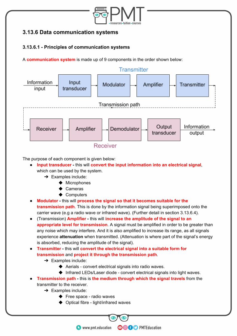
3.13.6 Data communication systems 3.13.6.1 - Principles of communication systems A communication system is made up of 9 components in the order shown below:
The purpose of each component is given below:
● Input transducer - this will convert the input information into an electrical signal, which can be used by the system. ➔ Examples include:
◆ Microphones ◆ Cameras ◆ Computers
● Modulator - this will process the signal so that it becomes suitable for the transmission path. This is done by the information signal being superimposed onto the carrier wave (e.g a radio wave or infrared wave). (Further detail in section 3.13.6.4).
● (Transmission) Amplifier - this will increase the amplitude of the signal to an appropriate level for transmission. A signal must be amplified in order to be greater than any noise which may interfere. And it is also amplified to increase its range, as all signals experience attenuation when transmitted. (Attenuation is where part of the signal’s energy is absorbed, reducing the amplitude of the signal).
● Transmitter - this will convert the electrical signal into a suitable form for transmission and project it through the transmission path. ➔ Examples include:
◆ Aerials - convert electrical signals into radio waves. ◆ Infrared LEDs/Laser diode - convert electrical signals into light waves.
● Transmission path - this is the medium through which the signal travels from the transmitter to the receiver. ➔ Examples include:
◆ Free space - radio waves ◆ Optical fibre - light/infrared waves
www.pmt.education

◆ Copper wire - electrical signals ● Receiver - this detects the transmitted signal and converts it back into an electrical
signal. ➔ Examples include:
◆ Aerials - radio waves ◆ Photodiode - light/infrared waves
● (Receiver) Amplifier - as mentioned above, when a signal is transmitted it becomes attenuated so the receiver amplifier will increase the amplitude of the signal to an appropriate level for further processing.
● Demodulator - this is used to separate the original information signal from the carrier wave, therefore will obtain the original signal.
● Output transducer - this will convert the signal into its required form. ➔ Examples include:
◆ Speakers - convert electrical signals to sound ◆ Printers - convert electrical signals to mechanical ◆ Projectors - convert electrical signals to light
3.13.6.2 - Transmission media There are three main types of transmission media: metal wire, optical fibre, and electromagnetic waves in the radio and microwave range. Metal wires made from materials such as copper form a direct connection between the transmitter and receiver and carry information in the form of electric current. These are used for short distances and low data transfers. A major disadvantage of metal wires is that they experience corrosion and oxidation which affects their performance. There are three types of metal wires that are used:
● Coaxial cable - this is made up of a central copper conductor, surrounded by an insulator, which in turn is surrounded by a braided metal shield, which protects the signal in the copper conductor from outside interference. The entire cable is covered by an outer insulating jacket which protects it from the environment.
○ This type of cable can only be used for short distances as the signal power halves every 5 m travelled.
○ It is not very secure. ○ It can transmit high frequency
signals up to 1 GHz.
Image source: Tkgd2007,CC BY 3.0
www.pmt.education
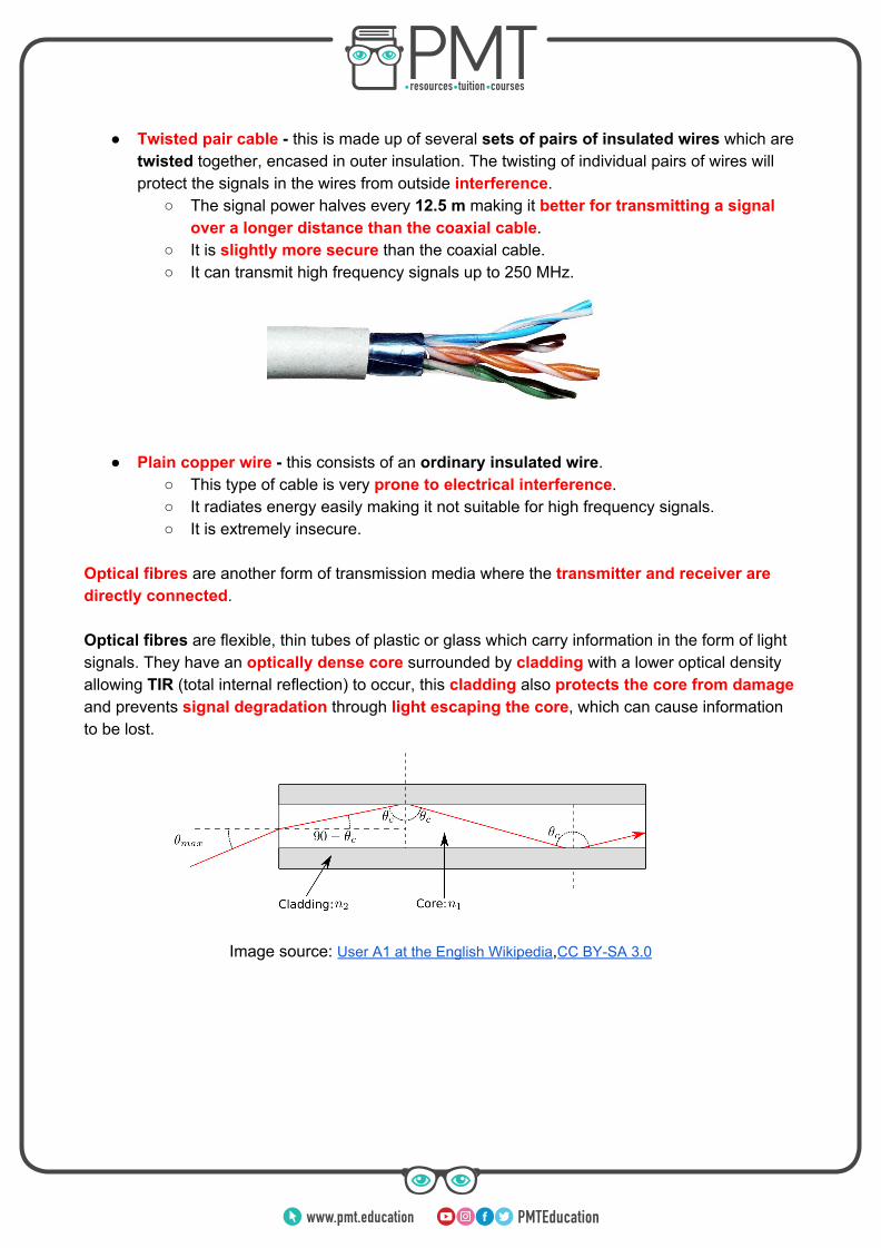
● Twisted pair cable - this is made up of several sets of pairs of insulated wires which are
twisted together, encased in outer insulation. The twisting of individual pairs of wires will protect the signals in the wires from outside interference.
○ The signal power halves every 12.5 m making it better for transmitting a signal over a longer distance than the coaxial cable.
○ It is slightly more secure than the coaxial cable. ○ It can transmit high frequency signals up to 250 MHz.
● Plain copper wire - this consists of an ordinary insulated wire. ○ This type of cable is very prone to electrical interference. ○ It radiates energy easily making it not suitable for high frequency signals. ○ It is extremely insecure.
Optical fibres are another form of transmission media where the transmitter and receiver are directly connected. Optical fibres are flexible, thin tubes of plastic or glass which carry information in the form of light signals. They have an optically dense core surrounded by cladding with a lower optical density allowing TIR (total internal reflection) to occur, this cladding also protects the core from damage and prevents signal degradation through light escaping the core, which can cause information to be lost.
Image source: User A1 at the English Wikipedia,CC BY-SA 3.0
www.pmt.education

Information can travel through an optical fibre at very high frequencies and due to the small size of fibres, hundreds can be included in an optical fibre cable, meaning that a huge volume of information can be transmitted at one time.
Image source: Buy_on_turbosquid_optical.jpg: Cable masterderivative work: Srleffler
,CC BY-SA 3.0 Some further advantages of optical fibres are that they are:
● Extremely secure - this is because it is not possible to intercept the signal within a fibre without first breaking into the fibre.
● Resistant to noise - this is because each fibre confines the light signals within it, and adjacent fibres do not cause interference.
● Cheap - this is because they are produced using glass, which is much cheaper than copper and much fewer optical fibres are needed to transfer the same amount of information as many metal wires.
Optical fibre repeaters are used to reduce the effect of absorption and dispersion (section 3.3.2.3) in an optical fibre. There are two types of optical fibres: ➔ Multi-mode - allows several rays of light to travel through it at once and relies on TIR.
Image source: Kebes,CC BY-SA 3.0, Image is cropped
➔ Single-mode - these fibres are much more narrow and difficult to make, meaning they are
more expensive than multimode fibres. As they are very narrow, the degree of dispersion in them is much lower.
Image source: Kebes,CC BY-SA 3.0, Image is cropped
www.pmt.education

Electromagnetic waves are used to transfer information when there is no physical connection between the transmitter and receiver, the electromagnetic waves travel through free space. EM waves are very easy to intercept, meaning they are potentially insecure, however data can be encrypted to increase security. EM waves are also affected by absorption and scattering in the atmosphere which will reduce their signal strength. There are three main ranges of frequencies of EM waves used for transmission:
● Longwave - Frequency: 150 kHz - 300 kHz, Wavelength: 1 - 2 km These types of signals can travel very long distances, due to their large wavelengths which allow them to diffract around obstacles (e.g hills and large structures) easily. Furthermore, due to the differences in refractive index of certain layers of the Earth’s atmosphere, longwave signals can travel as ground waves (surface waves), which move parallel to the Earth’s surface following its curvature. This means that transmitter and receiver do not need to be in line of sight of each other. Longwave signals are used to broadcast radio signals.
● Shortwave - Frequency: 3 MHz - 30 MHz, Wavelength: 10 - 100 m These types of signals can also travel very long distances, but they travel as skywaves. These are refracted and reflected by layers of different densities in the atmosphere for example the ionosphere, (and sometimes also the Earth) meaning they can travel far beyond the horizon. Shortwave signals are used in communication between ships and airplanes, and remote regions.
Image source: Sebastian Janke,CC BY-SA 2.5, Image is cropped
● Microwave - Frequency: 2 GHz - 100 GHz, Wavelength: 3 - 150 mm
These signals travel in straight lines (as effective diffraction does not occur) and so the transmitter and receiver must be within line of sight.
www.pmt.education

Microwave signals can carry a large amount of information and so are used in mobile networks (3G and 4G) and bluetooth devices.
Satellite systems can also be used to transfer information; satellites detect signals from Earth and re-transmit them so they can reach their intended locations. Satellites allow extremely long distance communication links. There are two main types of satellite orbit: ➔ Geostationary orbits - their orbital period is 24 hours and they always stay above the
same point on the Earth, because they orbit directly above the equator. These types of satellites are very useful for sending TV and telephone signals because they are always above the same point on the Earth so you don’t have to alter the plane of an aerial or transmitter. These are positioned 35786 km above Earth.
➔ Low-orbit satellites - these have significantly lower orbits in comparison to geostationary satellites, therefore they travel much faster meaning their orbital periods are much smaller. Because of this, these satellites require less powerful transmitters and can potentially orbit across the entire Earth’s surface, this makes them useful for monitoring the weather, making scientific observations about places which are unreachable and military applications. They can also be used for communications but because they travel so quickly, many satellites must work together to allow constant coverage for a certain region. As they have lower orbits, they are cheaper to launch and maintain than geostationary satellites.
An up-link is the transmission path from Earth to the satellite, while a down-link is the transmission path from the satellite to Earth. Because the transmitters on Earth are much more powerful than those found on satellites, the signal strength of the down-link is far lower than that of the up-link. To prevent the up-link from overwhelming (overlapping) the down-link, which would cause receivers to become de-sensed, the two links have different frequencies. Satellites use signals in the microwave region. There are several bands of frequencies used, below are the two most common ones:
● C-band - Up-link: 6 GHz, Down-link: 4 GHz ● Ku-band - Up-link: 14 GHz, Down-link: 11 GHz
www.pmt.education

The table below summarises the advantages and disadvantages of the 3 transmission media and satellite communication, which are described above:
Medium Data transmission rate Cost Security
Metal wire 10 Mbit s-1 - 1 Gbit s-1 More expensive than optical fibre when the data transmission rate is considered, otherwise cheaper
Low
Optical fibre 100 Tbit s-1 Expensive but better value than metal wire, as the transmission rate is much larger. Also multi-mode fibres are far cheaper than single-mode fibres.
Very high
EM waves through free
space
Depends on the type of transmission, ranges from
20 kbit s-1 - 275 Mbit s-1
No physical link so cheaper in that sense, however the transmitters and receivers can be very expensive
Low, however can be improved
through encryption of signals
Satellite Up to 50 Mbit s-1 Extremely high Low, however can be improved
through encryption of signals
3.13.6.3 - Time-division multiplexing Time-division multiplexing (TDM) is a way of increasing data transmission rates by combining many input signals, meaning they can travel as a continuous signal down the transmission path. This method works as follows:
➔ Each data stream is separated into packets and is allocated a defined time slot for
transmission. These packets will also contain information which will help identify the stream
www.pmt.education

from which it originated and synchronisation information, which allows the multiplexer and demultiplexer to remain in sync.
➔ The multiplexer will switch between data streams to allow transmission during their allocated time slot, maintaining a continuous flow of data down the transmission path.
➔ The demultiplexer must stay in sync with the multiplexer so that it can separate/demultiplex packets so that they can be recombined with others from the same data stream to ensure that the original data is received.
An important thing to note is that the bandwidth, which is the maximum data transfer rate, of the transmission medium must be larger than the bandwidth of the sending and receiving devices. The advantages of TDM are:
● It is relatively cheap. ● The bandwidth of the transmitted signal is never greater than the bandwidth of any
individual data stream. ● It allows data to be transmitted at a single frequency.
The disadvantages of TDM are:
● The rate of transmission of any individual data stream decreases as the number of data streams connected to the multiplexer increases.
● Even if a data stream has no data to send, a time slot is always formed, meaning part of the transmission path will be momentarily empty.
3.13.6.4 - Amplitude (AM) and frequency modulation (FM) techniques Modulation as mentioned previously, is the process which makes a signal suitable for the transmission path. Modulation is not always necessary, for example in a metal wire which can transfer electrical signals directly, however it is essential where the transmission media is an electromagnetic wave in free space. There are two types of modulation, amplitude modulation and frequency modulation, both of which are described below: Amplitude modulation is where the shape of the information signal will define the amplitude of the carrier wave. Here the information signal is the data which is being transferred, while the carrier wave is the medium in which this data must travel. This process is shown in the diagram below:
www.pmt.education

Image source: Ivan Akira,CC BY-SA 3.0, Image is cropped The information signal enters the modulator (labelled X) along with a carrier wave, where the information signal will be imprinted on the carrier wave’s amplitude. The modulated signal leaves on the left and will continue to an amplifier if it’s part of a communication system. The information signal, carrier wave and resultant modulated wave are shown more clearly on the amplitude-time graphs below.
Image source: Ivan Akira,CC BY-SA 3.0, Image is cropped
The process of amplitude modulation adds two bands of frequencies to the carrier signal:
● Upper sideband - this is equal to the sum of the carrier frequency (fC) and maximum frequency present in the information signal (fm)
pper sideband f U = C + fm ● Lower sideband - this is equal to the difference between the carrier frequency (fC) and
maximum frequency present in the information signal (fm) ower sideband f L = C − fm
www.pmt.education

Image source: Heron2,CC BY-SA 3.0
The bandwidth, which here is the range between the highest and lowest frequency in the signal, that is required to transfer the modulated signal can be found by calculating the difference between the lower and upper sidebands.
f ) f ) f ( C + fm − ( C − fm = 2 m In order to transmit this signal, the transmission medium must therefore be able to carry the above frequency (2fm), this is defined as the AM bandwidth.
M bandwidth f A = 2 m
Frequency modulation is where the amplitude of the information signal will define the frequency of the carrier wave (e.g the higher the amplitude of the information signal, the higher the frequency of the modulated signal). This process is shown below:
Image source: Ivan Akira,CC BY-SA 3.0, Image is cropped
Note how the amplitude of the modulated signal remains constant. Unlike in amplitude modulation, where two side frequencies are added, in frequency modulation, an infinite number of side frequencies are added:
www.pmt.education

The shape of the above graph can vary greatly and is dependent on the frequency deviation (Δf), which is the amount by which the information signal can change to carrier frequency. If the frequency deviation (Δf) is much less than the maximum frequency present in the information signal (fm), then the modulated signal is known as a narrowband FM. Whereas if this is not true, the modulated signal is known as a wideband FM, which are far more common.
As the side bands in a wideband frequency modulated signal extend to infinity, you cannot define bandwidth as easily as with amplitude modulated signals. However, Carson’s rule shows that 98% of a wideband FM signal is transmitted in the bandwidth given by:
M bandwidth (Δf ) F = 2 + fm Note that fm here is the maximum frequency in the modulated signal. Frequency modulation is far more complex than amplitude modulation, however it brings a number of advantages:
● FM is resistant to noise - this is because most types of noise will affect a signal’s amplitude and not its frequency, meaning that AM, on the other hand, is susceptible to noise. FM receivers can remove any noise added to the signal by making its amplitude constant, this process is called limiting.
www.pmt.education

● FM is less prone to fading - this is where reflected and refracted waves meet at the transmitter and interfere causing a change in amplitude, but as mentioned before, amplitude is limited so this has no effect on the signal.
However, FM also has its disadvantages:
● FM usually requires a larger bandwidth - this also means that when used for broadcasting, it must be used at higher frequencies where there is available room.
● Transmitters and receivers must be line of sight - this is true when the signal has a high frequency as it cannot be effectively refracted. This is why car radios have to be re-tuned when driving across long distances.
The data capacity of a transmission channel is the maximum rate of transmission and can be calculated by finding double its maximum possible bandwidth.
ata capacity 2 aximum available bandwidth D = × m The table below compares the available bandwidth for several transmission media:
Transmission media Bandwidth
Coaxial cable 1010
Twisted-pair cable 109
Optical fibre 1016
www.pmt.education