Embed Size (px)
Citation preview
Designing with the Nios II Processor
and SOPC Builder
Exercise Manual
Software Requirements: Quartus II 8.1
ModelSim 6.3g (for Quartus II 8.1)
Nios II 8.1
Altera Megacores IP 8.1
Hardware Requirements:
This lab guide is set up to allow you to use the following boards:
Nios Development Kits: Stratix 1S10 and 1S10ES
Stratix 1S40
Stratix II 2S60 and Stratix 2S60ES
Cyclone 1C20
Cyclone II 2C35 and 2C35ES
Cyclone III Starter FPGA and Nios II Embedded
Evaluation Kits (NEEK)
Lead-Free (rohs) Kits: Stratix II 2S60 and Stratix 2S60ES
Cyclone II 2C35 and 2C35ES
Cyclone III FPGA Starter Kit
Cyclone III Nios II Evaluation (NEEK) Kit
DSP Development Kits: Stratix II 2S60 and 2S60ES

Exercise Manual Designing with the Nios II Processor & SOPC Builder (Day 1)
Copyright © 2008 Altera Corporation A-MNL-NIIHW-EX-8-1-v1
2

Exercise Manual Designing with the Nios II Processor & SOPC Builder (Day 1)
Copyright © 2008 Altera Corporation A-MNL-NIIHW-EX-8-1-v1
3
Lab 1
Creating a Nios II
Processor System

Exercise Manual Designing with the Nios II Processor & SOPC Builder (Day 1)
Copyright © 2008 Altera Corporation A-MNL-NIIHW-EX-8-1-v1
4

Exercise Manual Designing with the Nios II Processor & SOPC Builder (Day 1)
Copyright © 2008 Altera Corporation A-MNL-NIIHW-EX-8-1-v1
5
Objectives:
Over the course of the lab today, you will create an embedded hardware system and run some
software code on it. As the lab progresses, you will continue to modify your hardware system
to incorporate new features as you learn about them in class.
This lab guide is set up to allow you to use any one of the following development kits, so,
some written steps will pertain to one type of board; other steps to another type of board.
You can tell when type of kit your are using by looking at the labelling on the FPGA package
on your kit. Failing that, the instructor should be able to advise you. The kits fall into two
main categories as shown below:
Nios II Processor Development Kits:
Stratix Stratix II
Stratix 1S10 Stratix II 2S60
Stratix 1S10ES Stratix II 2S60ES
Stratix 1S40 Stratix II 2S60 rohs (new lead-free kit)
Cyclone Cyclone II Cyclone III
Cyclone 1C20 Cyclone II 2C35 FPGA Starter Kit
Cyclone II 2C35ES Nios II Evaluation (NEEK)
-and-
DSP Development Kits:
Stratix II
Stratix II 2S60
2S60ES
Note: It is unlikely that you will using a DSP kit unless you are also taking the DSP class.

Exercise Manual Designing with the Nios II Processor & SOPC Builder (Day 1)
Copyright © 2008 Altera Corporation A-MNL-NIIHW-EX-8-1-v1
6
Step 1: Set Up Embedded Hardware Design Project
Hardware set up requirements:
• USB-Blaster, ByteBlaster, ByteBlaster II, or Byte Blaster MV programming cable
connected between computer and JTAG connection header on development board
• Power supply connected to the board
Typical Nios II Processor Development Kit
1. Insert the CD Rom from the back of your handout into the computer provided.
2. Open the CD Rom for viewing, and double-click on the .exe file you see. It will be called
“NII_SOPCBuilder_2Day_<ver>.exe.”
This is a self-extracting zip file that will unzip the files you need for today into the folder
called, C:\altera_trn\Nios II_HW\NiosII_2Day.
3. Navigate into that directory and then into Day1.
In this directory, you will find several sub-directories for each of the different types of
development boards supported for this class. Inside each respective project folder is a
sub-directory called niosII_lab that contains the partially completed Quartus II project
that you will use as your starting point today.
Note: Do not connect LCD
display to board even
though it is shown in the
figure – you will not be
using it today.
Exercise Manual Designing with the Nios II Processor & SOPC Builder (Day 1)
Copyright © 2008 Altera Corporation A-MNL-NIIHW-EX-8-1-v1
7
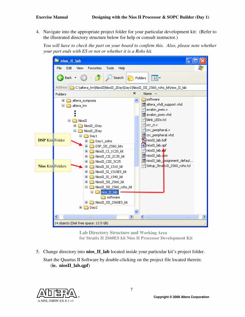
4. Navigate into the appropriate project folder for your particular development kit: (Refer to
the illustrated directory structure below for help or consult instructor.)
You will have to check the part on your board to confirm this. Also, please note whether
your part ends with ES or not or whether it is a Rohs kit.
Lab Directory Structure and Working Area
for Stratix II 2S60ES kit Nios II Processor Development Kit
5. Change directory into nios_II_lab located inside your particular kit’s project folder.
Start the Quartus II Software by double-clicking on the project file located therein:
(ie. niosII_lab.qpf)
DSP Kits Folder
Nios Kits Folders
Exercise Manual Designing with the Nios II Processor & SOPC Builder (Day 1)
Copyright © 2008 Altera Corporation A-MNL-NIIHW-EX-8-1-v1
8
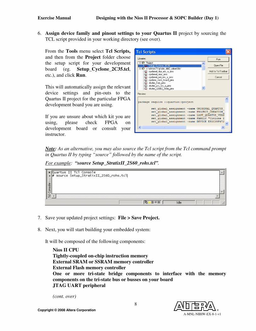
6. Assign device family and pinout settings to your Quartus II project by sourcing the
TCL script provided in your working directory (see over).
From the Tools menu select Tcl Scripts,
and then from the Project folder choose
the setup script for your development
board (eg. Setup_Cyclone_2C35.tcl,
etc.), and click Run.
This will automatically assign the relevant
device settings and pin-outs to the
Quartus II project for the particular FPGA
development board you are using.
If you are unsure about which kit you are
using, please check FPGA on
development board or consult your
instructor.
Note: As an alternative, you may also source the Tcl script from the Tcl command prompt
in Quartus II by typing “source” followed by the name of the script.
For example: “source Setup_StratixII_2S60_rohs.tcl”.
7. Save your updated project settings: File > Save Project.
8. Next, you will start building your embedded system:
It will be composed of the following components:
Nios II CPU
Tightly-coupled on-chip instruction memory
External SRAM or SSRAM memory controller
External Flash memory controller
One or more tri-state bridge components to interface with the memory
components on the tri-state bus or busses on your board
JTAG UART peripheral
(cont. over)

Exercise Manual Designing with the Nios II Processor & SOPC Builder (Day 1)
Copyright © 2008 Altera Corporation A-MNL-NIIHW-EX-8-1-v1
9
.
.
.
PIO peripherals, configured to interface to LEDs, buttons, and a seven segment
display if your board has one
System clock timer
High resolution timer
System ID peripheral
PLL
Note: Some of these component’s settings will depend on what kit you have. Please
follow the instructions for your particular board, and choose appropriately. Consult
with the instructor if you are not sure which board you have.
In essence, you will be building a system that looks like this:
Outline of Hardware System
9. Start SOPC Builder from Tools => SOPC Builder… and enter the system name, niosII,
when the next window pops up. You can choose VHDL or Verilog (whichever you
prefer) as the implementation language. The blank SOPC builder window will open.

Exercise Manual Designing with the Nios II Processor & SOPC Builder (Day 1)
Copyright © 2008 Altera Corporation A-MNL-NIIHW-EX-8-1-v1
10
10. The Device Family should match the FPGA you are using (eg. Stratix II EP2S60.
Ensure the External Clock frequency is set to 50 MHz for all kits (except the Stratix II
DSP kits, whose input frequency is to be set to 100 MHz).

Exercise Manual Designing with the Nios II Processor & SOPC Builder (Day 1)
Copyright © 2008 Altera Corporation A-MNL-NIIHW-EX-8-1-v1
11
Step 2: Add Nios II Processor to System
1. From the left hand window pane select Nios II Processor and click Add. Select Nios
II/s for the processor core. Select DSP Block as the Hardware Multiply option for all
Stratix boards, Embedded Multipliers for all Cyclone II and Cyclone III boards, or
Logic Elements for Cyclone boards.

Exercise Manual Designing with the Nios II Processor & SOPC Builder (Day 1)
Copyright © 2008 Altera Corporation A-MNL-NIIHW-EX-8-1-v1
12
2. Click on the Caches and Memory Interfaces tab. Set the Instruction Cache size to
4Kbytes and include one tightly coupled memory instruction master port.

Exercise Manual Designing with the Nios II Processor & SOPC Builder (Day 1)
Copyright © 2008 Altera Corporation A-MNL-NIIHW-EX-8-1-v1
13
3. Now, click on the JTAG Debug Module tab. Select the JTAG Target Connection
Download Level 3 option. This will provide us with all the debug options listed on that
tab.
4. Click Finish. This will add it to the SOPC Builder system.

Exercise Manual Designing with the Nios II Processor & SOPC Builder (Day 1)
Copyright © 2008 Altera Corporation A-MNL-NIIHW-EX-8-1-v1
14
5. Rename the processor, if necessary, by right clicking on it and selecting Rename.
Type in cpu and hit enter.
Note: It is essential for you to enter the
names of all peripherals and memories
EXACTLY as shown in the lab guide since
these components will be referenced later
on in the C–code. Also, be sure that you
type each name using the correct CASE.

Exercise Manual Designing with the Nios II Processor & SOPC Builder (Day 1)
Copyright © 2008 Altera Corporation A-MNL-NIIHW-EX-8-1-v1
15
Step 3: Add Avalon-MM Tristate Bridge (or Bridges) to System
1. You will now add the appropriate number of Avalon-MM-to-tri-state bus-bridging
peripheral/s required to let you access the various memory chips on your board. (After
this you will add the appropriate memory interface controllers, themselves.)
You will find the Avalon-MM Tri-State Bridge peripheral in the Bridges and
Adapters section of the SOPC Builder pick-list under Memory-Mapped components.
For all the boards, you will add at least one tri-state bridge. Others will require two tri-
state bridges. Follow the upcoming steps to see what is required of your board.
2. For all boards, add an Avalon-MM Tri-State Bridge peripheral to the design. Select
the Registered option, and click Finish.
Exercise Manual Designing with the Nios II Processor & SOPC Builder (Day 1)
Copyright © 2008 Altera Corporation A-MNL-NIIHW-EX-8-1-v1
16
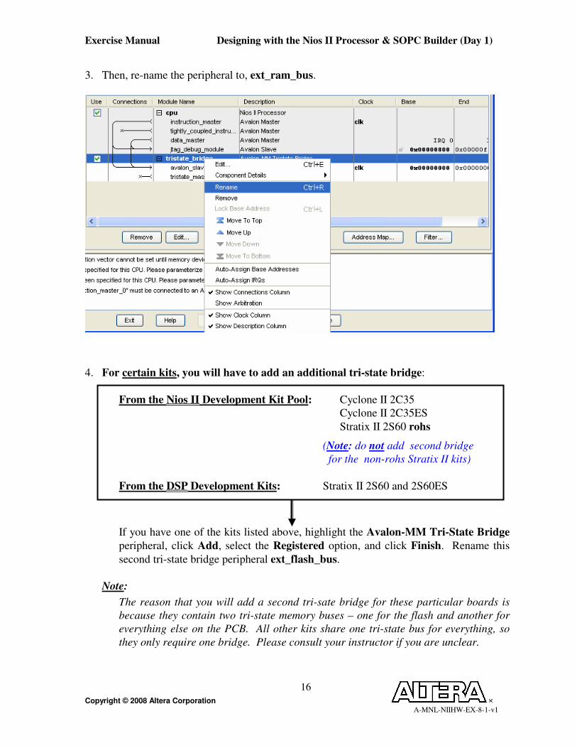
3. Then, re-name the peripheral to, ext_ram_bus.
4. For certain kits, you will have to add an additional tri-state bridge:
From the Nios II Development Kit Pool: Cyclone II 2C35
Cyclone II 2C35ES
Stratix II 2S60 rohs
(Note: do not add second bridge
for the non-rohs Stratix II kits)
From the DSP Development Kits: Stratix II 2S60 and 2S60ES
If you have one of the kits listed above, highlight the Avalon-MM Tri-State Bridge
peripheral, click Add, select the Registered option, and click Finish. Rename this
second tri-state bridge peripheral ext_flash_bus.
Note:
The reason that you will add a second tri-sate bridge for these particular boards is
because they contain two tri-state memory buses – one for the flash and another for
everything else on the PCB. All other kits share one tri-state bus for everything, so
they only require one bridge. Please consult your instructor if you are unclear.
Exercise Manual Designing with the Nios II Processor & SOPC Builder (Day 1)
Copyright © 2008 Altera Corporation A-MNL-NIIHW-EX-8-1-v1
17
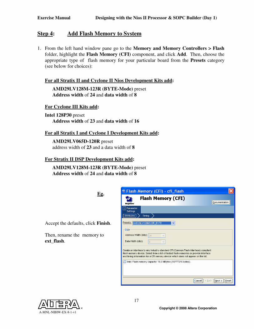
Step 4: Add Flash Memory to System
1. From the left hand window pane go to the Memory and Memory Controllers > Flash
folder, highlight the Flash Memory (CFI) component, and click Add. Then, choose the
appropriate type of flash memory for your particular board from the Presets category
(see below for choices):
For all Stratix II and Cyclone II Nios Development Kits add:
AMD29LV128M-123R (BYTE-Mode) preset
Address width of 24 and data width of 8
For Cyclone III Kits add:
Intel 128P30 preset
Address width of 23 and data width of 16
For all Stratix I and Cyclone I Development Kits add:
AMD29LV065D-120R preset
address width of 23 and a data width of 8
For Stratix II DSP Development Kits add:
AMD29LV128M-123R (BYTE-Mode) preset
Address width of 24 and data width of 8
Eg.
Accept the defaults, click Finish.
Then, rename the memory to
ext_flash.
Exercise Manual Designing with the Nios II Processor & SOPC Builder (Day 1)
Copyright © 2008 Altera Corporation A-MNL-NIIHW-EX-8-1-v1
18
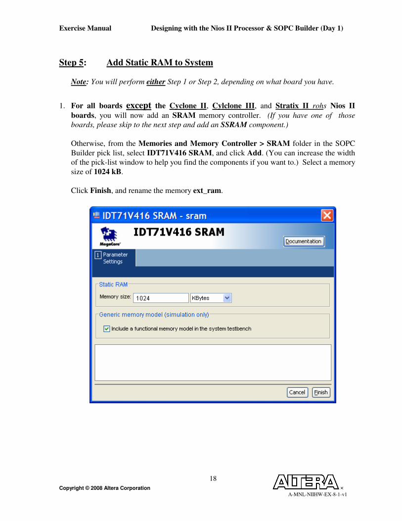
Step 5: Add Static RAM to System
Note: You will perform either Step 1 or Step 2, depending on what board you have.
1. For all boards except the Cyclone II, Cylclone III, and Stratix II rohs Nios II
boards, you will now add an SRAM memory controller. (If you have one of those
boards, please skip to the next step and add an SSRAM component.)
Otherwise, from the Memories and Memory Controller > SRAM folder in the SOPC
Builder pick list, select IDT71V416 SRAM, and click Add. (You can increase the width
of the pick-list window to help you find the components if you want to.) Select a memory
size of 1024 kB.
Click Finish, and rename the memory ext_ram.
Exercise Manual Designing with the Nios II Processor & SOPC Builder (Day 1)
Copyright © 2008 Altera Corporation A-MNL-NIIHW-EX-8-1-v1
19
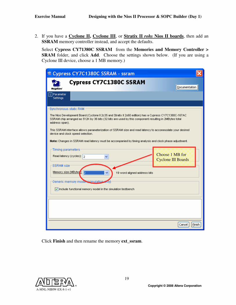
2. If you have a Cyclone II, Cyclone III, or Stratix II rohs Nios II boards, then add an
SSRAM memory controller instead, and accept the defaults.
Select Cypress CY71380C SSRAM from the Memories and Memory Controller >
SRAM folder, and click Add. Choose the settings shown below. (If you are using a
Cyclone III device, choose a 1 MB memory.)
Click Finish and then rename the memory ext_ssram.
Choose 1 MB for
Cyclone III Boards

Exercise Manual Designing with the Nios II Processor & SOPC Builder (Day 1)
Copyright © 2008 Altera Corporation A-MNL-NIIHW-EX-8-1-v1
20
3. Now, highlight the RAM component you just created, and move it up directly underneath
the ext_ram_bus peripheral using the Move Up button located at the bottom of the work
space. (Note: Doing this is not absolutely necessary but will help keep the System
Contents page nice and tidy as you start adding more components and adjusting master-
slave connections.)
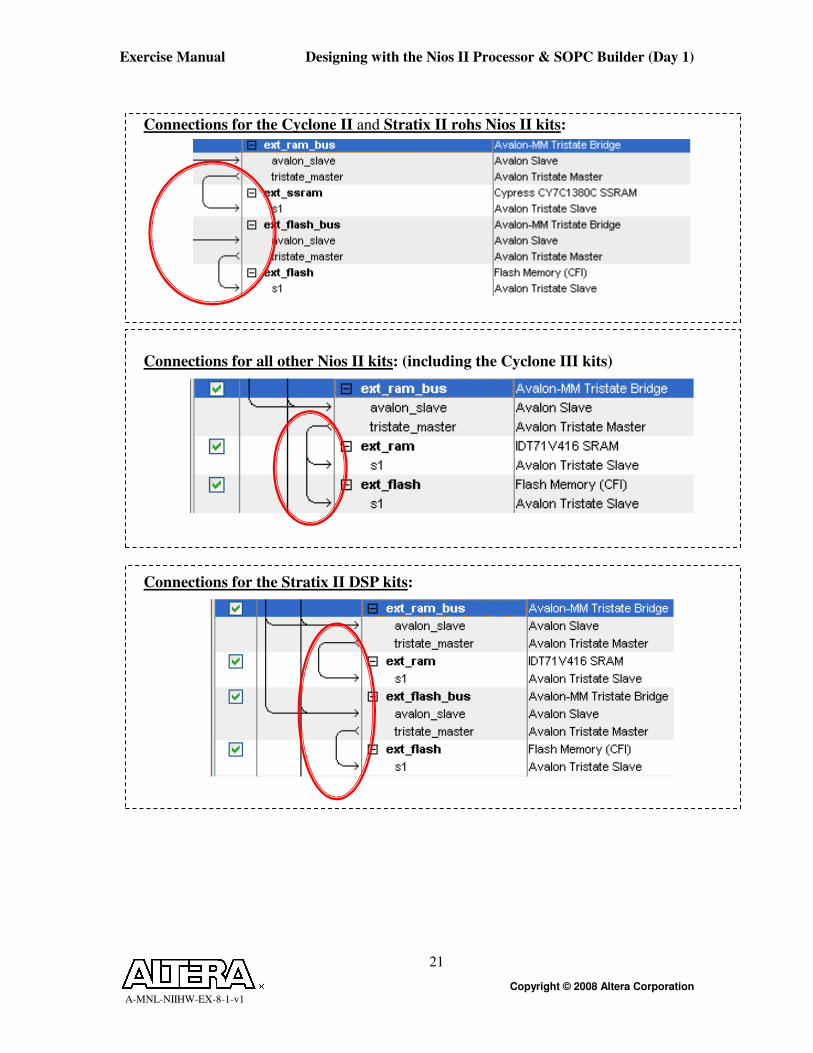
4. Ensure that the appropriate master slave connections are set in the connections panel in
SOPC Builder. That is, the “ext_ram_bus” peripheral tri-state master should master the
“ext_ram” (or “ext_ssram”) memory, and the “ext_flash_bus,” if present, should master
“ext_flash” memory. To do this, go to the View menu in SOPC Builder, and unless it is
already done so for you, turn on Show Connections Column. (A check mark will
appear beside your selection.)
Experiment by moving your mouse over the connection panel the view to highlight either
the interconnects or the master-slave connections. You can click on the circles in the
interconnect to make or sever the connections. Black dots mean that the connection will
be made; while white dots mean that no connection will be made (see below and see
over).
move mouse to change
connection view as shown
Edit Mode View Mode
Exercise Manual Designing with the Nios II Processor & SOPC Builder (Day 1)
Copyright © 2008 Altera Corporation A-MNL-NIIHW-EX-8-1-v1
21
Connections for the Cyclone II and Stratix II rohs Nios II kits:
Connections for all other Nios II kits: (including the Cyclone III kits)
Connections for the Stratix II DSP kits:

Exercise Manual Designing with the Nios II Processor & SOPC Builder (Day 1)
Copyright © 2008 Altera Corporation A-MNL-NIIHW-EX-8-1-v1
22
Step 6: Set Connection Properties For Shared Avalon-Tristate Bridge
1. For the following boards only, set the ext_ram_bus tri-state bridge peripheral to
share address ports between the ext_ram and the ext_flash peripherals as shown below:
Cyclone 1C20
Cyclone III FPGA Starter kit
Nios II Evaluation (NEEK)
Stratix 1S10 and 1S10ES
Stratix 1S40
Stratix 2S60 and 2S60ES
Note: Double-click on the peripheral
To open it for editing.
This is required for these kits because they have only one tri-state peripheral, so you have
to share some pins through it.
Then click Finish.

Exercise Manual Designing with the Nios II Processor & SOPC Builder (Day 1)
Copyright © 2008 Altera Corporation A-MNL-NIIHW-EX-8-1-v1
23
Step 7: Add JTAG UART to System
1. From the left hand window pane find the JTAG UART from the Interface Protocols >
Serial folder and click Add. Accept the defaults. (The screen should appear as shown.)
The peripheral should be named jtag_uart.
Exercise Manual Designing with the Nios II Processor & SOPC Builder (Day 1)
Copyright © 2008 Altera Corporation A-MNL-NIIHW-EX-8-1-v1
24
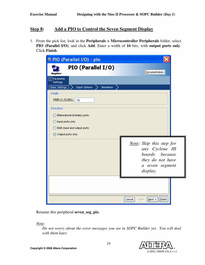
Step 8: Add a PIO to Control the Seven Segment Display
1. From the pick list, look in the Peripherals > Microcontroller Peripherals folder, select
PIO (Parallel I/O), and click Add. Enter a width of 16 bits, with output ports only.
Click Finish.
Rename this peripheral seven_seg_pio.
Note:
Do not worry about the error messages you see in SOPC Builder yet. You will deal
with them later.
Note: Skip this step for
any Cyclone III
boards because
they do not have
a seven segment
display.

Exercise Manual Designing with the Nios II Processor & SOPC Builder (Day 1)
Copyright © 2008 Altera Corporation A-MNL-NIIHW-EX-8-1-v1
25
Step 9: Add Another PIO to Control the LEDs
1. Add a second PIO (Parallel I/O) peripheral with a width of 8 bits (or 4 bits for the
Cyclone III boards), with output ports only set. Click Finish. Rename this peripheral
led_pio.
Choose 4 for
Cyclone III Boards
Exercise Manual Designing with the Nios II Processor & SOPC Builder (Day 1)
Copyright © 2008 Altera Corporation A-MNL-NIIHW-EX-8-1-v1
26
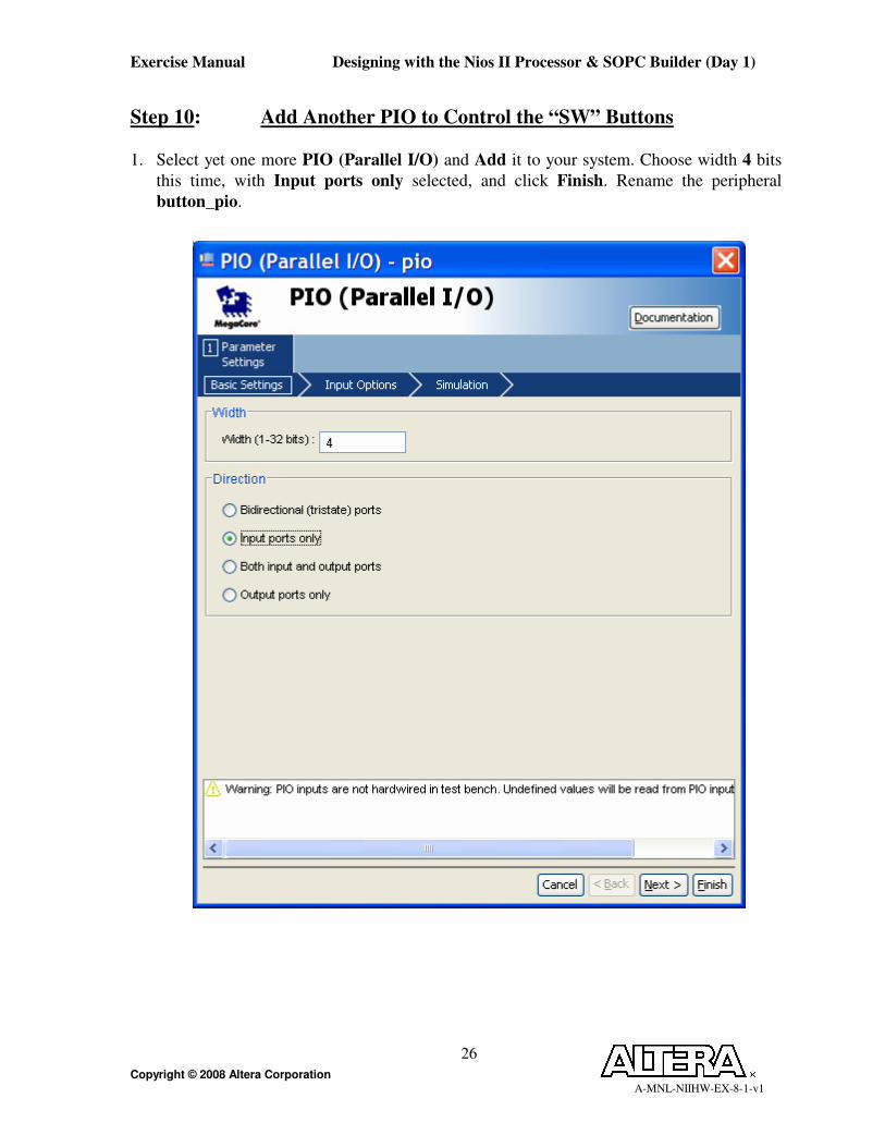
Step 10: Add Another PIO to Control the “SW” Buttons
1. Select yet one more PIO (Parallel I/O) and Add it to your system. Choose width 4 bits
this time, with Input ports only selected, and click Finish. Rename the peripheral
button_pio.

Exercise Manual Designing with the Nios II Processor & SOPC Builder (Day 1)
Copyright © 2008 Altera Corporation A-MNL-NIIHW-EX-8-1-v1
27
Step 11: Add Timers to System
1. Select the Interval Timer from the Microcontroller Peripherals folder and click Add.
Select the Full-Featured Preset, and click Finish. After the timer has been added to your
system, rename it to sys_clk_timer.

Exercise Manual Designing with the Nios II Processor & SOPC Builder (Day 1)
Copyright © 2008 Altera Corporation A-MNL-NIIHW-EX-8-1-v1
28
2. From the left hand window pane add another Interval Timer to the system. Change the
Preset to Full-featured and the period to usec. Then click Finish. (You are going to use
this later when you time the speed of some of our software functions.)
Rename the timer to high_res_timer.
Exercise Manual Designing with the Nios II Processor & SOPC Builder (Day 1)
Copyright © 2008 Altera Corporation A-MNL-NIIHW-EX-8-1-v1
29
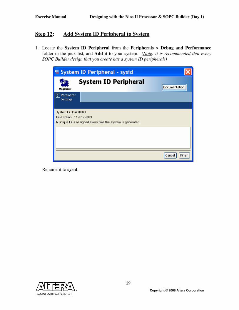
Step 12: Add System ID Peripheral to System
1. Locate the System ID Peripheral from the Peripherals > Debug and Performance
folder in the pick list, and Add it to your system. (Note: it is recommended that every
SOPC Builder design that you create has a system ID peripheral!)
Rename it to sysid.

Exercise Manual Designing with the Nios II Processor & SOPC Builder (Day 1)
Copyright © 2008 Altera Corporation A-MNL-NIIHW-EX-8-1-v1
30
Step 13: Add PLL Peripheral to System
1. Now, Add the Altera PLL component to the project from the PLL folder. Then launch
the ALTPLL MegaWizard and configure the PLL using the settings shown below.
(Note: You navigate through the Wizard using the Next button.)
Exercise Manual Designing with the Nios II Processor & SOPC Builder (Day 1)
Copyright © 2008 Altera Corporation A-MNL-NIIHW-EX-8-1-v1
31
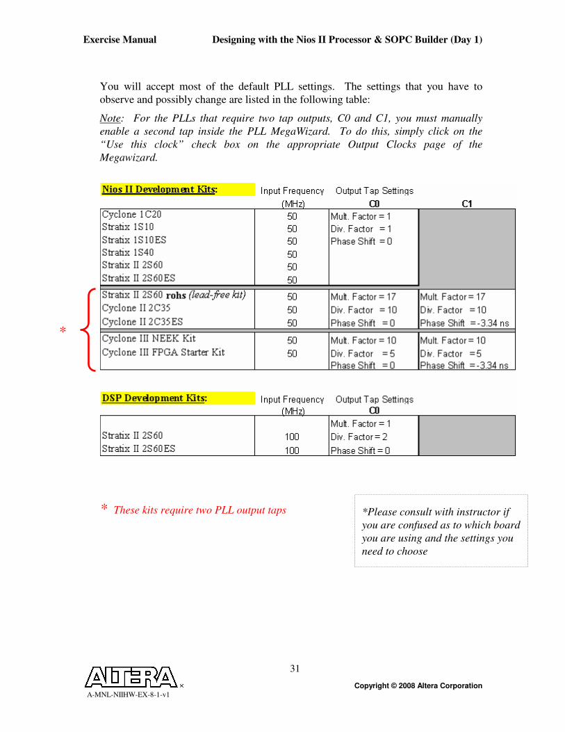
You will accept most of the default PLL settings. The settings that you have to
observe and possibly change are listed in the following table:
Note: For the PLLs that require two tap outputs, C0 and C1, you must manually
enable a second tap inside the PLL MegaWizard. To do this, simply click on the
“Use this clock” check box on the appropriate Output Clocks page of the
Megawizard.
* These kits require two PLL output taps *Please consult with instructor if
you are confused as to which board
you are using and the settings you
need to choose
*
Exercise Manual Designing with the Nios II Processor & SOPC Builder (Day 1)
Copyright © 2008 Altera Corporation A-MNL-NIIHW-EX-8-1-v1
32
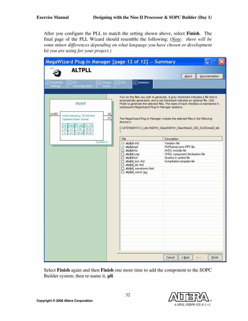
After you configure the PLL to match the setting shown above, select Finish. The
final page of the PLL Wizard should resemble the following: (Note: there will be
some minor differences depending on what language you have chosen or development
kit you are using for your project.)
Select Finish again and then Finish one more time to add the component to the SOPC
Builder system; then re-name it, pll.
Exercise Manual Designing with the Nios II Processor & SOPC Builder (Day 1)
Copyright © 2008 Altera Corporation A-MNL-NIIHW-EX-8-1-v1
33
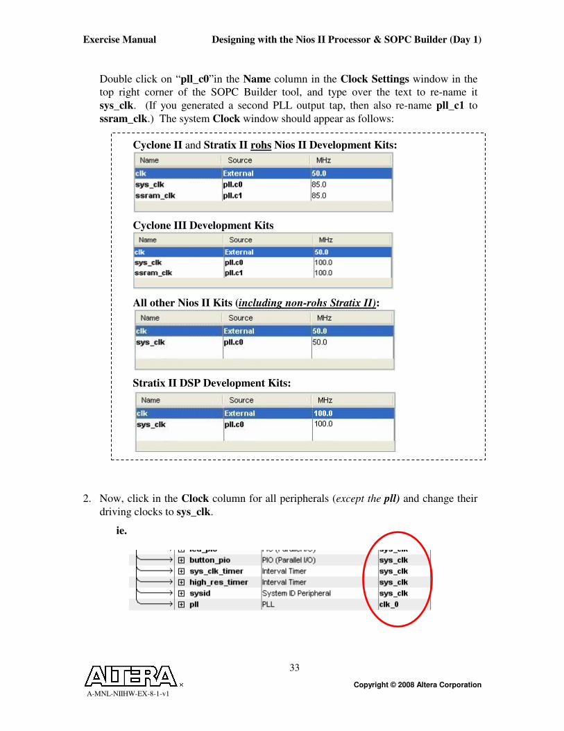
Double click on “pll_c0”in the Name column in the Clock Settings window in the
top right corner of the SOPC Builder tool, and type over the text to re-name it
sys_clk. (If you generated a second PLL output tap, then also re-name pll_c1 to
ssram_clk.) The system Clock window should appear as follows:
Cyclone II and Stratix II rohs Nios II Development Kits:
Cyclone III Development Kits
All other Nios II Kits (including non-rohs Stratix II):
Stratix II DSP Development Kits:
2. Now, click in the Clock column for all peripherals (except the pll) and change their
driving clocks to sys_clk.
ie.
Exercise Manual Designing with the Nios II Processor & SOPC Builder (Day 1)
Copyright © 2008 Altera Corporation A-MNL-NIIHW-EX-8-1-v1
34
Step 14: Establish IRQ Priorities
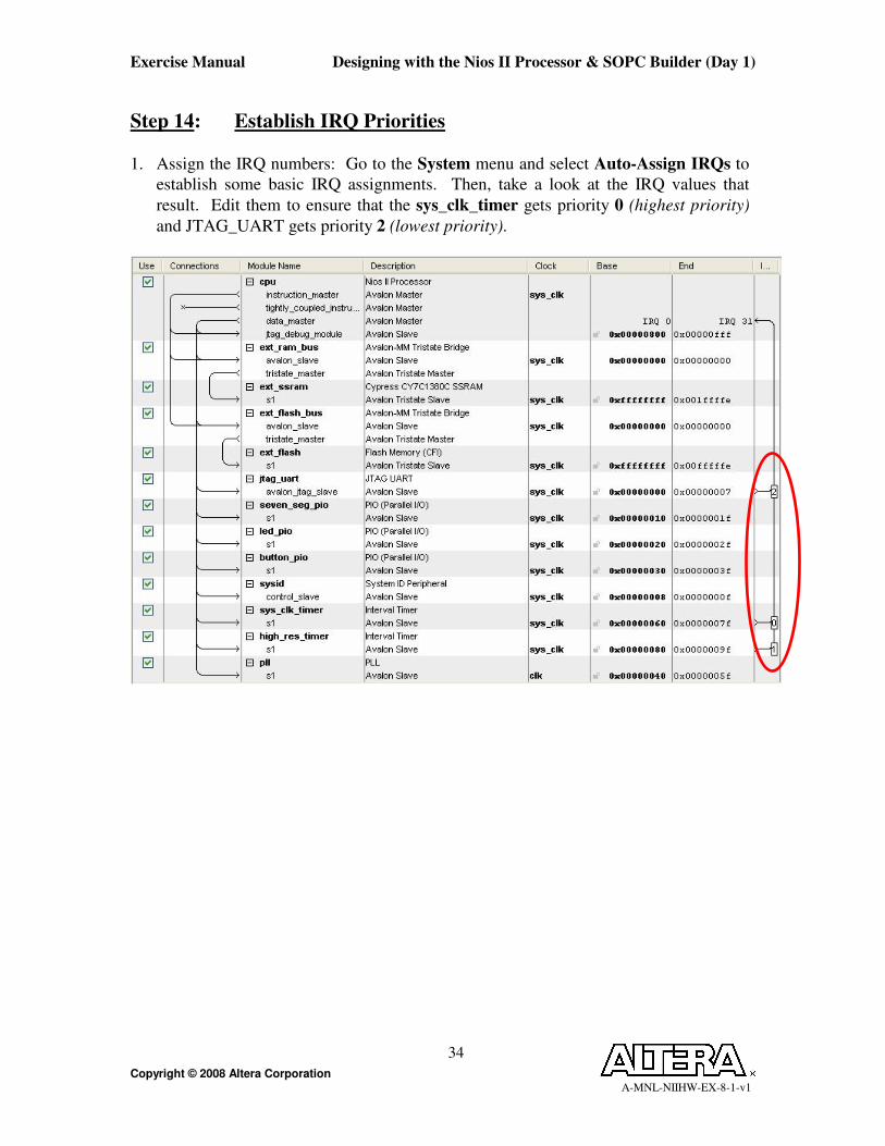
1. Assign the IRQ numbers: Go to the System menu and select Auto-Assign IRQs to
establish some basic IRQ assignments. Then, take a look at the IRQ values that
result. Edit them to ensure that the sys_clk_timer gets priority 0 (highest priority)
and JTAG_UART gets priority 2 (lowest priority).
Exercise Manual Designing with the Nios II Processor & SOPC Builder (Day 1)
Copyright © 2008 Altera Corporation A-MNL-NIIHW-EX-8-1-v1
35
Step 15: Add Tightly Coupled On-Chip Memory to System
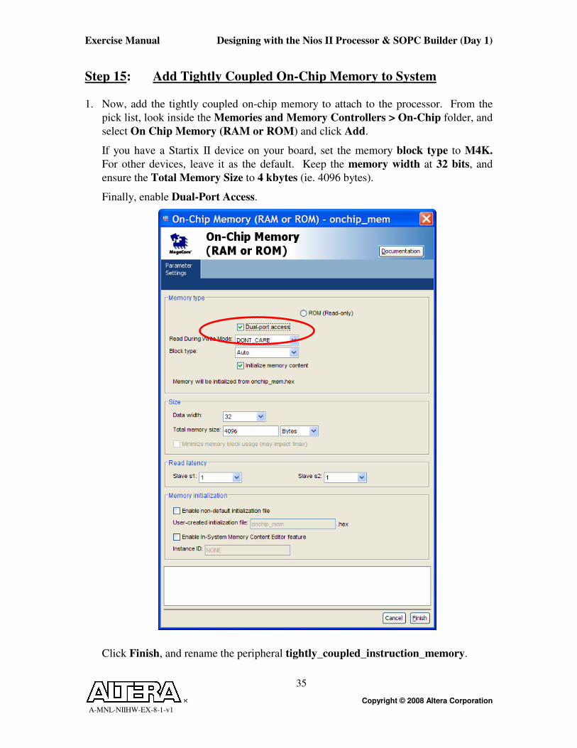
1. Now, add the tightly coupled on-chip memory to attach to the processor. From the
pick list, look inside the Memories and Memory Controllers > On-Chip folder, and
select On Chip Memory (RAM or ROM) and click Add.
If you have a Startix II device on your board, set the memory block type to M4K.
For other devices, leave it as the default. Keep the memory width at 32 bits, and
ensure the Total Memory Size to 4 kbytes (ie. 4096 bytes).
Finally, enable Dual-Port Access.
Click Finish, and rename the peripheral tightly_coupled_instruction_memory.

Exercise Manual Designing with the Nios II Processor & SOPC Builder (Day 1)
Copyright © 2008 Altera Corporation A-MNL-NIIHW-EX-8-1-v1
36
2. Change the clock driving both tightly coupled memory ports to sys_clk, if necessary, and
using the Move up button, move the peripheral up in the system contents page until it
resides directly underneath the cpu. (This will make it easier to see its connections to the
cpu.)
3. Ensure that the appropriate master/slave connections are made between the cpu and the
Tightly Coupled Memory.
Toggling the System Interconnect Fabric Connections:
Click your mouse on the appropriate dots in the tightly coupled memory’s connectivity
diagram in order to toggle the connections as shown below: (Note: the connected state is
solid; while the disconnected state is white.)
Port S1 of the tightly_coupled_instruction_memory should be connected to the cpu’s
tightly_coupled_instruction_master_0 master port, and port S2 should connect to the
cpu’s data_master port.
4. You will now change the base addresses of the tightly coupled master ports (S1 and S2)
so that they do not overlap any of the other peripherals in the design.
5. As a first step, go to the System menu and choose Auto Assign Base Addresses for the
system. A number of error messages will disappear.
6. Next, look in the SOPC Builder message window (toward the top), and find the cpu
warning message that suggests where you can locate your tightly coupled memories in the
memory map to produce optimal performance. You will have to scroll the message
window to the right to see the entire message.

Exercise Manual Designing with the Nios II Processor & SOPC Builder (Day 1)
Copyright © 2008 Altera Corporation A-MNL-NIIHW-EX-8-1-v1
37
For instance, it may suggest that you locate both ports of the tightly
_coupled_instruction_memory to at least base address 0x02402000. Whatever the
case, double-click in the Base address box and edit the values to their recommended
settings as shown.
Then lock the values (right-click > Lock Base Address).
Example:
Step 16: Take a Look at Your System
1. To again ensure that all base addresses are valid, go to the system menu or right click on
any one of the base addresses in the table and select Auto-Assign Base Addresses.
2. Your SOPC Builder System Contents page should now appear similar to the following:
For the Nios II Cyclone II and Stratix II rohs kits:

Exercise Manual Designing with the Nios II Processor & SOPC Builder (Day 1)
Copyright © 2008 Altera Corporation A-MNL-NIIHW-EX-8-1-v1
38
For the Cyclone III kits:
For all other Nios II kits:

Exercise Manual Designing with the Nios II Processor & SOPC Builder (Day 1)
Copyright © 2008 Altera Corporation A-MNL-NIIHW-EX-8-1-v1
39
For the Stratix II DSP kits:
Exercise Manual Designing with the Nios II Processor & SOPC Builder (Day 1)
Copyright © 2008 Altera Corporation A-MNL-NIIHW-EX-8-1-v1
40
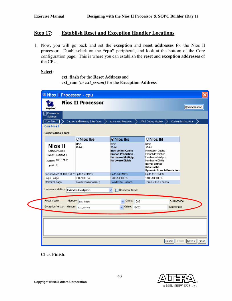
Step 17: Establish Reset and Exception Handler Locations
1. Now, you will go back and set the exception and reset addresses for the Nios II
processor. Double-click on the “cpu” peripheral, and look at the bottom of the Core
configuration page: This is where you can establish the reset and exception addresses of
the CPU.
Select:
ext_flash for the Reset Address and
ext_ram (or ext_ssram) for the Exception Address
Click Finish.
Exercise Manual Designing with the Nios II Processor & SOPC Builder (Day 1)
Copyright © 2008 Altera Corporation A-MNL-NIIHW-EX-8-1-v1
41
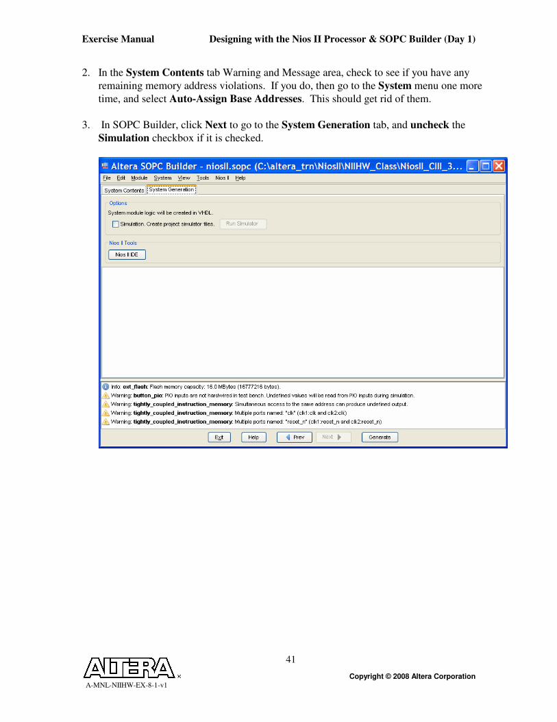
2. In the System Contents tab Warning and Message area, check to see if you have any
remaining memory address violations. If you do, then go to the System menu one more
time, and select Auto-Assign Base Addresses. This should get rid of them.
3. In SOPC Builder, click Next to go to the System Generation tab, and uncheck the
Simulation checkbox if it is checked.
Exercise Manual Designing with the Nios II Processor & SOPC Builder (Day 1)
Copyright © 2008 Altera Corporation A-MNL-NIIHW-EX-8-1-v1
42
4. Save your SOPC Builder system (File > Save).
5. Next, click Generate. SOPC Builder will now create the parameterized SOPC system.
Note: If you happen to receive a warning message in SOPC Builder that prevents you
from generating the system, check to make sure that all the peripherals are connected to
sys_clk. For example, you might encounter a message like:
the cpu/tightly_coupled_instruction_master_0 may connect to 1 slave only
If setting sys_clk does not solve your problem, you may have to close SOPC Builder and
then re-open it again in order to register the change you just made.
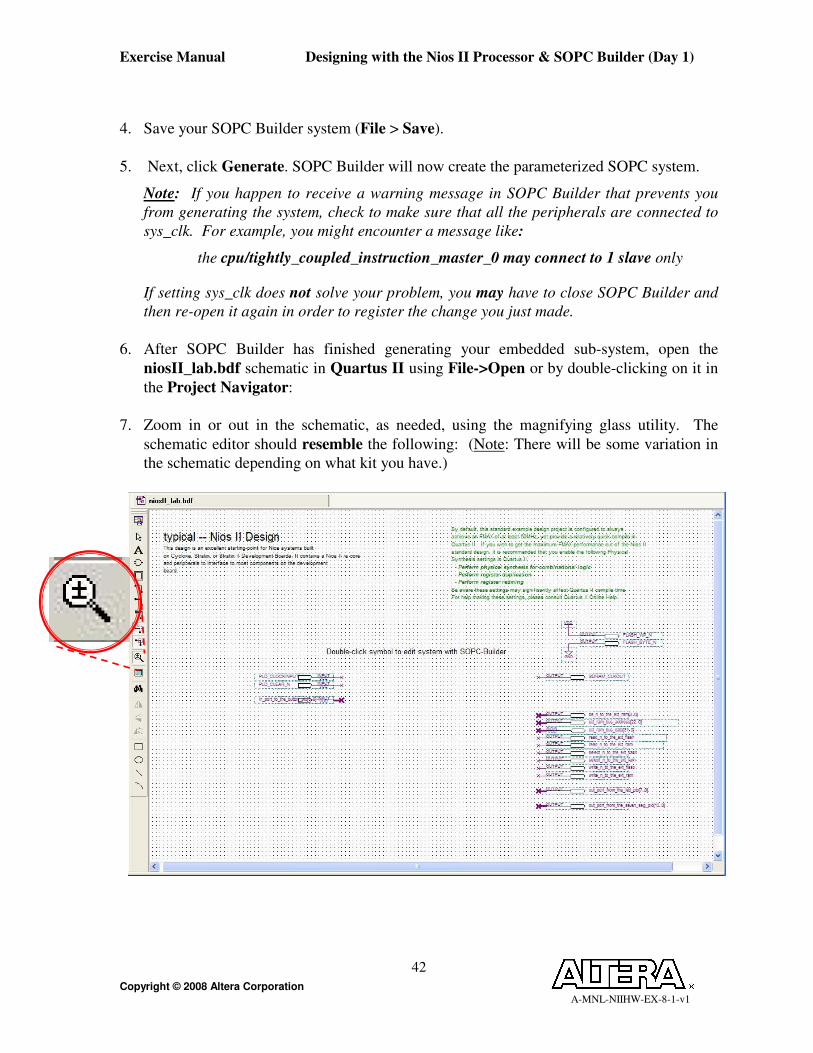
6. After SOPC Builder has finished generating your embedded sub-system, open the
niosII_lab.bdf schematic in Quartus II using File->Open or by double-clicking on it in
the Project Navigator:
7. Zoom in or out in the schematic, as needed, using the magnifying glass utility. The
schematic editor should resemble the following: (Note: There will be some variation in
the schematic depending on what kit you have.)
Exercise Manual Designing with the Nios II Processor & SOPC Builder (Day 1)
Copyright © 2008 Altera Corporation A-MNL-NIIHW-EX-8-1-v1
43
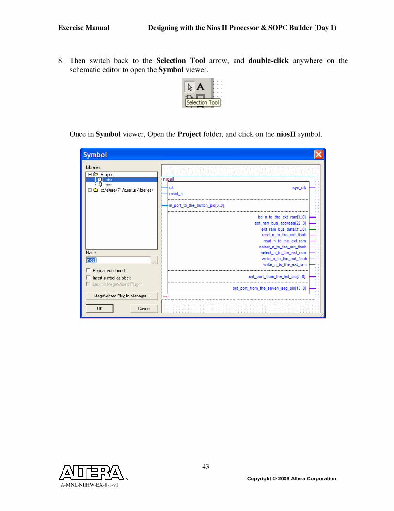
8. Then switch back to the Selection Tool arrow, and double-click anywhere on the
schematic editor to open the Symbol viewer.
Once in Symbol viewer, Open the Project folder, and click on the niosII symbol.

Exercise Manual Designing with the Nios II Processor & SOPC Builder (Day 1)
Copyright © 2008 Altera Corporation A-MNL-NIIHW-EX-8-1-v1
44
9. The block symbols for each, respective, system should appear as follows:
Cyclone II and Stratix II rohs Nios II development kit systems:
clk
reset_n
in_port_to_the_button_pio[3..0]
ssram_clk
sys_clk
address_to_the_ext_flash[23..0]
read_n_to_the_ext_flash
select_n_to_the_ext_flash
w rite_n_to_the_ext_flash
address_to_the_ext_ssram[20..0]
adsc_n_to_the_ext_ssram
bw _n_to_the_ext_ssram[3..0]
bw e_n_to_the_ext_ssram
chipenable1_n_to_the_ext_ssram
outputenable_n_to_the_ext_ssram
out_port_from_the_led_pio[7..0]
out_port_from_the_seven_seg_pio[15..0]
data_to_and_from_the_ext_flash[7..0]
data_to_and_from_the_ext_ssram[31..0]
NiosII
inst
Cyclone III systems:
clk
reset_n
in_port_to_the_button_pio[3..0]
sys_clk
be_n_to_the_ext_ram[3..0]
ext_ram_bus_address[22..0]
read_n_to_the_ext_flash
read_n_to_the_ext_ram
select_n_to_the_ext_flash
select_n_to_the_ext_ram
w rite_n_to_the_ext_f lash
w rite_n_to_the_ext_ram
out_port_from_the_led_pio[7..0]
out_port_from_the_seven_seg_pio[15..0]
ext_ram_bus_data[31..0]
niosII
inst
DSP board systems:
clk
reset_n
in_port_to_the_button_pio[3..0]
sys_clk
address_to_the_ext_f lash[23..0]
read_n_to_the_ext_flash
select_n_to_the_ext_flash
w rite_n_to_the_ext_flash
address_to_the_ext_ram[19..0]
be_n_to_the_ext_ram[3..0]
read_n_to_the_ext_ram
select_n_to_the_ext_ram
w rite_n_to_the_ext_ram
out_port_from_the_led_pio[7..0]
out_port_from_the_seven_seg_pio[15..0]
data_to_and_from_the_ext_flash[7..0]
data_to_and_from_the_ext_ram[31..0]
NiosII
inst
All other Nios II development kit systems:

10. Add the niosII component to your Quartus II project by pressing OK; then drop the
symbol into your schematic so that it’s pins line up exactly with the pin placements as
shown below. These pinouts have already been done for you.
Note: If the pins do not all line up exactly, then you will need to go back to SOPC
Builder and re-check your work.
Cyclone II and Stratix II rohs Nios II Development Kit systems will resemble this figure:
(Please refer to the schematic that corresponds to your particular development kit.)

Exercise Manual Designing with the Nios II Processor & SOPC Builder (Day 1)
Copyright © 2008 Altera Corporation A-MNL-NIIHW-EX-8-1-v1
46
All Cyclone III Kit systems will resemble this figure:
All other Nios II Development kit systems will resemble this figure:
Exception: For the regular (ie. non-rohs) Stratix II Nios II development kits, the bus
width of the flash address is actually 24 bits (ie. ext_ram_bus_address[23..0]) because of
the flash selection you chose.

Exercise Manual Designing with the Nios II Processor & SOPC Builder (Day 1)
Copyright © 2008 Altera Corporation A-MNL-NIIHW-EX-8-1-v1
47
While Stratix II DSP Development Kit systems will look like this:
11. Save the schematic (File > Save).
12. Save the Quartus II project (File > Save Project).
13. .Start compilation in Quartus II. by selecting Start Compilation from the Processing
menu.
14. When compilation completes, select OK.
You will continue from this point during the next lab.
END OF LAB 1

Exercise Manual Designing with the Nios II Processor & SOPC Builder (Day 1)
Copyright © 2008 Altera Corporation A-MNL-NIIHW-EX-8-1-v1
48

Exercise Manual Designing with the Nios II Processor & SOPC Builder (Day 1)
Copyright © 2008 Altera Corporation A-MNL-NIIHW-EX-8-1-v1
49
Lab 2
Software Flow

Exercise Manual Designing with the Nios II Processor & SOPC Builder (Day 1)
Copyright © 2008 Altera Corporation A-MNL-NIIHW-EX-8-1-v1
50

Exercise Manual Designing with the Nios II Processor & SOPC Builder (Day 1)
Copyright © 2008 Altera Corporation A-MNL-NIIHW-EX-8-1-v1
51
1. You will now download the Nios II FPGA design created in the previous lab to the Nios
development board.
Within Quartus II, go to the Tools menu, and select the Programmer. (If the .sof file
for your project does not populate the File field then click on the Add File button .
Then select file niosII_lab.sof and click Open.)
2. Tick the Program/Configure checkbox for that .sof file, and then click the Start
Programming icon .
If the Start Programming button is not enabled, make sure your Hardware Setup field (at
the top of the Programmer window) reads USB-Blaster or Byteblaster. If not, click on
the Hardware Setup button and choose USB-Blaster or Byteblaster from the drop-down
menu, and click Close.
3. Launch the Nios II IDE from SOPC Builder (see Nios II menu > Nios II IDE). Select
OK if the Nios II IDE Workspace Launcher dialog box appears.
4. Go to the Nios II IDE Workbench, and create a new software project by selecting New-
>Project from the File menu. Select Nios II C/C++ Application, and press Next.
Exercise Manual Designing with the Nios II Processor & SOPC Builder (Day 1)
Copyright © 2008 Altera Corporation A-MNL-NIIHW-EX-8-1-v1
52
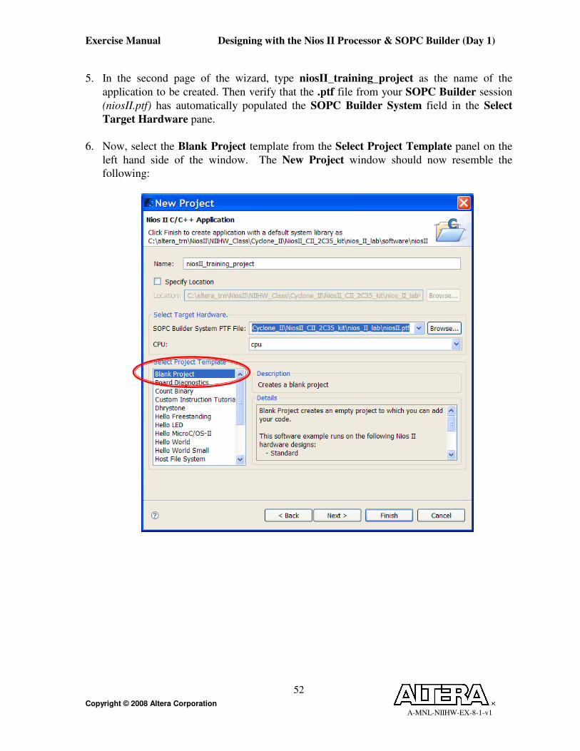
5. In the second page of the wizard, type niosII_training_project as the name of the
application to be created. Then verify that the .ptf file from your SOPC Builder session
(niosII.ptf) has automatically populated the SOPC Builder System field in the Select
Target Hardware pane.
6. Now, select the Blank Project template from the Select Project Template panel on the
left hand side of the window. The New Project window should now resemble the
following:

Exercise Manual Designing with the Nios II Processor & SOPC Builder (Day 1)
Copyright © 2008 Altera Corporation A-MNL-NIIHW-EX-8-1-v1
53
7. Press Next, and select:
Create a new system library named: niosII_training_project_syslib.
Then, click Finish.
8. You have now created two new projects in the Nios II IDE - a Nios II C/C++
Application project and a system library project. However, the Nios II C/C++
Application project is blank and you need to add some source code to it.
To add the file, simple.c, to the project, first expand the niosII_training_project folder
in the Nios II IDE.
Then, from within Windows, browse to
~NiosII_2Day\<your_particular_kit>\nios_II_lab\software, and find simple.c.

Exercise Manual Designing with the Nios II Processor & SOPC Builder (Day 1)
Copyright © 2008 Altera Corporation A-MNL-NIIHW-EX-8-1-v1
54
Drag simple.c into the niosII_training_project folder in the Nios II IDE as illustrated:
9. Now, highlight the niosII_training_project_syslib folder, right-click, and select
Properties.
Then, choose System Library from the left hand side of the Properties window. Ensure
that the stdout, stderr and stdin devices are set to jtag_uart and that the System clock
timer is set to sys_clk_timer.
For all boards except the Cyclone II board, set the Read-only data, Read/write memory,
and Program Memory fields to ext_ram. (For Cyclone II, set it to ext_ssram.)
Please refer to the figure on the next page.
drag

Exercise Manual Designing with the Nios II Processor & SOPC Builder (Day 1)
Copyright © 2008 Altera Corporation A-MNL-NIIHW-EX-8-1-v1
55
10. Click OK.
11. Compile the program by highlighting the niosII_training_project folder in the Nios II
C/C++ Projects window; then right-click and select Build Project.
Note: You can choose to run this command in the background when prompted. This will
free up the tool, letting you continue to use it for other tasks; whereas, running it in the
foreground causes you wait for it to complete.
12. After the compiler has finished, download and run the program on the development
board:
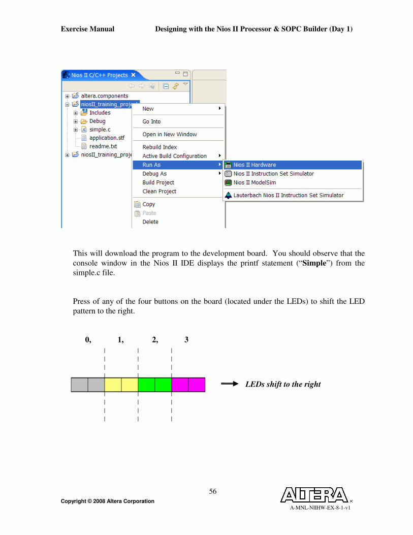
Highlight the niosII_training_project folder then right-click and select
Run As-> Nios II Hardware. (see over)
Note 1: If Run terminates before the code downloads to your board, and you get a
message pertaining to the JTAG download cable. then select Run > Run…
and from the Target Connection tab choose the appropriate download cable
that you are using and then press Apply and Run (or see instructor).
Note 2: The Nios II IDE will actually Build the project automatically for you if you
just click Run As -> Nios II Hardware without you having to explicitly go
through the Build step. You can enable or disable this option in the Window
> Preferences.
Exercise Manual Designing with the Nios II Processor & SOPC Builder (Day 1)
Copyright © 2008 Altera Corporation A-MNL-NIIHW-EX-8-1-v1
56
This will download the program to the development board. You should observe that the
console window in the Nios II IDE displays the printf statement (“Simple”) from the
simple.c file.
Press of any of the four buttons on the board (located under the LEDs) to shift the LED
pattern to the right.
0, 1, 2, 3
LEDs shift to the right
Exercise Manual Designing with the Nios II Processor & SOPC Builder (Day 1)
Copyright © 2008 Altera Corporation A-MNL-NIIHW-EX-8-1-v1
57
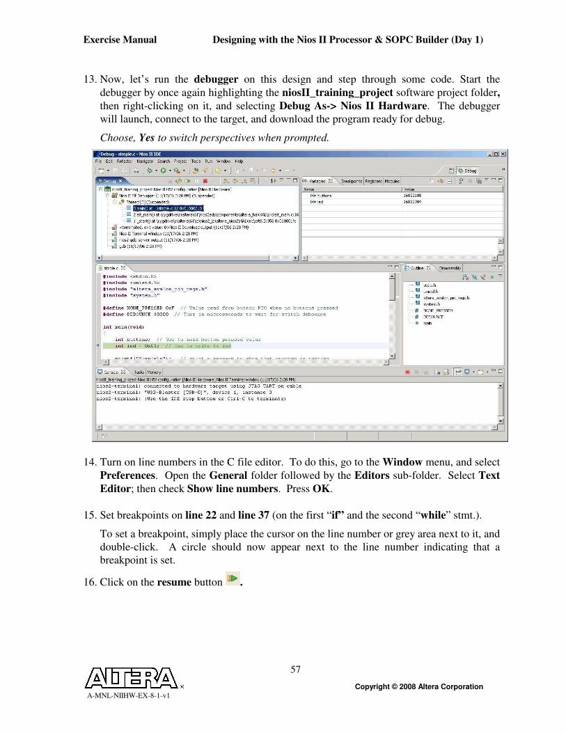
13. Now, let’s run the debugger on this design and step through some code. Start the
debugger by once again highlighting the niosII_training_project software project folder,
then right-clicking on it, and selecting Debug As-> Nios II Hardware. The debugger
will launch, connect to the target, and download the program ready for debug.
Choose, Yes to switch perspectives when prompted.
14. Turn on line numbers in the C file editor. To do this, go to the Window menu, and select
Preferences. Open the General folder followed by the Editors sub-folder. Select Text
Editor; then check Show line numbers. Press OK.
15. Set breakpoints on line 22 and line 37 (on the first “if” and the second “while” stmt.).
To set a breakpoint, simply place the cursor on the line number or grey area next to it, and
double-click. A circle should now appear next to the line number indicating that a
breakpoint is set.
16. Click on the resume button .
Exercise Manual Designing with the Nios II Processor & SOPC Builder (Day 1)
Copyright © 2008 Altera Corporation A-MNL-NIIHW-EX-8-1-v1
58
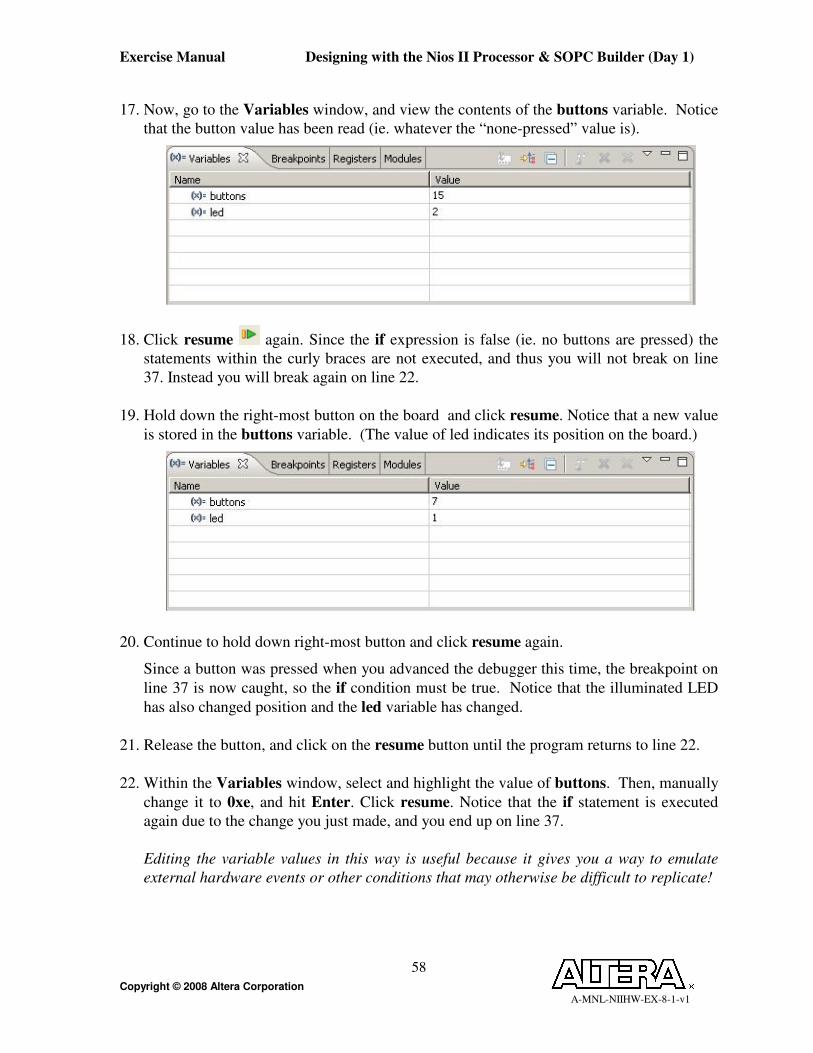
17. Now, go to the Variables window, and view the contents of the buttons variable. Notice
that the button value has been read (ie. whatever the “none-pressed” value is).
18. Click resume again. Since the if expression is false (ie. no buttons are pressed) the
statements within the curly braces are not executed, and thus you will not break on line
37. Instead you will break again on line 22.
19. Hold down the right-most button on the board and click resume. Notice that a new value
is stored in the buttons variable. (The value of led indicates its position on the board.)
20. Continue to hold down right-most button and click resume again.
Since a button was pressed when you advanced the debugger this time, the breakpoint on
line 37 is now caught, so the if condition must be true. Notice that the illuminated LED
has also changed position and the led variable has changed.
21. Release the button, and click on the resume button until the program returns to line 22.
22. Within the Variables window, select and highlight the value of buttons. Then, manually
change it to 0xe, and hit Enter. Click resume. Notice that the if statement is executed
again due to the change you just made, and you end up on line 37.
Editing the variable values in this way is useful because it gives you a way to emulate
external hardware events or other conditions that may otherwise be difficult to replicate!

Exercise Manual Designing with the Nios II Processor & SOPC Builder (Day 1)
Copyright © 2008 Altera Corporation A-MNL-NIIHW-EX-8-1-v1
59
23. Now terminate and remove the program. Go to the Debug sub-menu menu; right-
click on the software project thread, and select Terminate and Remove.

Exercise Manual Designing with the Nios II Processor & SOPC Builder (Day 1)
Copyright © 2008 Altera Corporation A-MNL-NIIHW-EX-8-1-v1
60
Exercise Manual Designing with the Nios II Processor & SOPC Builder (Day 1)
Copyright © 2008 Altera Corporation A-MNL-NIIHW-EX-8-1-v1
61
Optional Section:
Use the System Console to exercise your SOPC Builder System
Run System Console script from Nios II Command Shell
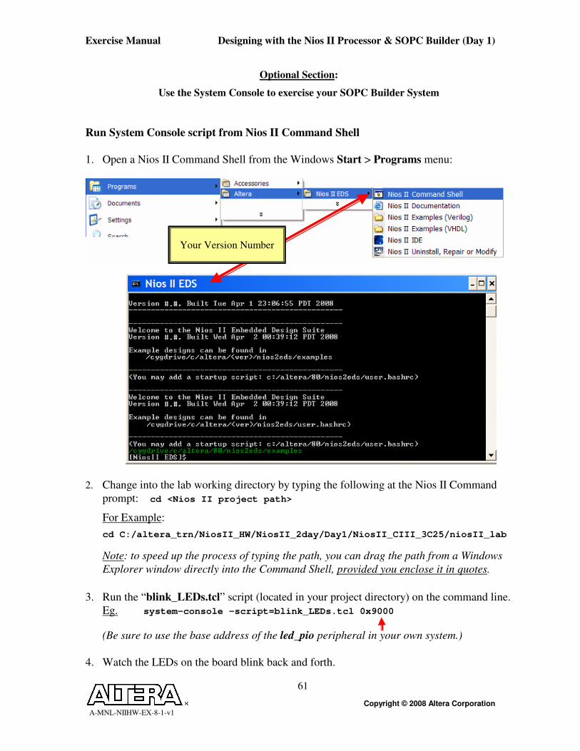
1. Open a Nios II Command Shell from the Windows Start > Programs menu:
2. Change into the lab working directory by typing the following at the Nios II Command
prompt: cd <Nios II project path>
For Example:
cd C:/altera_trn/NiosII_HW/NiosII_2day/Day1/NiosII_CIII_3C25/niosII_lab
Note: to speed up the process of typing the path, you can drag the path from a Windows
Explorer window directly into the Command Shell, provided you enclose it in quotes.
3. Run the “blink_LEDs.tcl” script (located in your project directory) on the command line.
Eg. system-console -script=blink_LEDs.tcl 0x9000
(Be sure to use the base address of the led_pio peripheral in your own system.)
4. Watch the LEDs on the board blink back and forth.
Your Version Number

Exercise Manual Designing with the Nios II Processor & SOPC Builder (Day 1)
Copyright © 2008 Altera Corporation A-MNL-NIIHW-EX-8-1-v1
62
5. You are now controlling the board without any software intervention!
For your information, the system-console script is listed below:
# -----------------------------------------------------------
# Runs an led "lightshow" for the specified number of times
#
# Sample Usage: system-console -script=blink_LEDs.tcl 0x9000
# -----------------------------------------------------------
proc run_led_lightshow { master addr count } {
#
# Set the values to write to the LED pio:
set led_vals {0 1 2 4 8 4 2 1}
#
# Write the values to LED's address:
open_service master $master
while { $count>0 } {
foreach val $led_vals {
master_write_8 $master $addr $val
#
# Insert some delay...
#
for { set i 1 } { $i <= 15000 } { incr i } {}
}
incr count -1
}
master_write_8 $master $addr 0x0
close_service master $master
}
# -----------------------------------------------------------
# Main:
# -----------------------------------------------------------
if {$argv0 != "system-console"} {
set jtag_master [lindex [get_service_paths master] 0]
# Handle the command line arguments...or lack thereof.
if { [llength $argv] > 0 } {
set led_base_addr [lindex $argv 0]
} else {
# If no command line arguments are provided,
# set default value for base_addr
set led_base_addr 0x0
}
processor_stop $jtag_master
puts ""
# Run LED light show (5 times):
run_led_lightshow $jtag_master $led_base_addr 5
puts ""
}
END OF LAB 2

Exercise Manual Designing with the Nios II Processor & SOPC Builder (Day 1)
Copyright © 2008 Altera Corporation A-MNL-NIIHW-EX-8-1-v1
63
Lab 3
RTL Simulation

Exercise Manual Designing with the Nios II Processor & SOPC Builder (Day 1)
Copyright © 2008 Altera Corporation A-MNL-NIIHW-EX-8-1-v1
64

Exercise Manual Designing with the Nios II Processor & SOPC Builder (Day 1)
Copyright © 2008 Altera Corporation A-MNL-NIIHW-EX-8-1-v1
65
In this lab you will use ModelSim-Altera to perform a hardware simulation of the processor
running code out of SRAM memory.
1. In SOPC Builder, the simulation model of the JTAG UART’s can be configured to
generate a data stream to send to the host processor.
To set this up, return to the SOPC Builder System Contents page, and double click on the
jtag_uart peripheral in order to re-open it. When the dialog box opens, click on the
Simulation tab. Select the Create ModelSim alias to open an interactive
stimulus/response radio button, and then hit Finish.
Exercise Manual Designing with the Nios II Processor & SOPC Builder (Day 1)
Copyright © 2008 Altera Corporation A-MNL-NIIHW-EX-8-1-v1
66
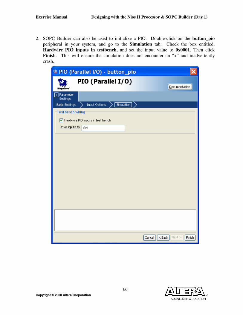
2. SOPC Builder can also be used to initialize a PIO. Double-click on the button_pio
peripheral in your system, and go to the Simulation tab. Check the box entitled,
Hardwire PIO inputs in testbench, and set the input value to 0x0001. Then click
Finish. This will ensure the simulation does not encounter an “x” and inadvertently
crash.
Exercise Manual Designing with the Nios II Processor & SOPC Builder (Day 1)
Copyright © 2008 Altera Corporation A-MNL-NIIHW-EX-8-1-v1
67
3. Before attempting to simulate, make sure that the path to the ModelSim software is set up
correctly:
a. Within SOPC Builder, choose Tools > Options > HDL Simulator Options. Then,
ensure that Mentor Graphics ModelSim-Altera. has been selected as the HDL
Simulator.
b. Now, unless the following field has already been populated, browse to the directory
where the ModelSim executables are located. For ModelSim-Altera, the directory is
<ModelSim install directory>\win32aloem.
For example: C:\altera\<ver>\modelsim_ae\win32aloem
c. Click Finish.
4. Navigate to the System Generation tab in SOPC Builder, and check the Simulation box
if it is not already enabled.
5. Save your system (File > Save).
6. Now, re-Generate the system by pressing the SOPC Builder Generate button.
Note: During system generation, SOPC Builder will re-create your system and produce
all of the files necessary for simulation except for the memory initialization files.
They need to be generated by the Nios II IDE in an upcoming step.
7. Once the system has been generated, you will finish the simulation set up by returning to
the Nios II IDE.
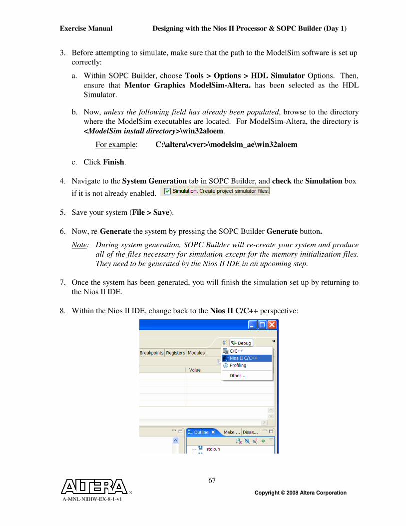
8. Within the Nios II IDE, change back to the Nios II C/C++ perspective:

Exercise Manual Designing with the Nios II Processor & SOPC Builder (Day 1)
Copyright © 2008 Altera Corporation A-MNL-NIIHW-EX-8-1-v1
68
9. Then, modify the system library parameters for your software project. You will need to
specify which memory you wish to compile code into and whether you want enhance the
simulation of your system by reducing code overhead. To do this, right click on the
system library project, niosII_training_project_syslib[niosII], and select Properties.
10. Next, from the Properties page, select System Library. Recall that this page controls
which communication devices in your design should be used for standard input / output
and also which memories your code gets assigned to.
o Select ext_ram (or ext_ssram) as Program, Read-only, and Read/write memory
and keep jtag_uart as stdout, stderr and stdin
o Enable the ModelSim only, no hardware support simulation feature
o Click OK
Note: Checking the ModelSim only, no hardware support checkbox tells the compiler
that the current project is being run on a simulator. The compiler will, in turn,
remove sections of the start-up code to improve simulation speed. Note that the
resulting software image will not run on a target board.
11. In the Nios II C/C++ Projects panel of the Nios II IDE, re-build the
niosII_training_project by highlighting and right-clicking on it, then selecting Build
Project.
Note: Once build completes, the file “ext_ram.dat” (or “ext_ssram.dat”) will be created
and initialized in the ~niosII_lab/niosII_sim folder. It contains the executable
image of the simple.c file that was compiled by the Nios II IDE and will be used
by ModelSim.
12. Once build completes, use the Nios II IDE to launch ModelSim. Again, highlight the
niosII_training_project, but this time select Run As > Nios II ModelSim.
If the ModelSim path has not been set properly, then you may be prompted to set it within
the Nios II IDE. Be sure that you are pointing to the version of ModelSim located in the
installation folder for the version of Quartus II that you are doing the labs with.

Exercise Manual Designing with the Nios II Processor & SOPC Builder (Day 1)
Copyright © 2008 Altera Corporation A-MNL-NIIHW-EX-8-1-v1
69
--------------------------------------------------------------------------------------------------------------
13. This should open the ModelSim project generated by SOPC Builder.
Note: If you encounter an error in this step, however, and the project does not open
properly, then your will simply need to manually open the Modelsim project
(niosII_sim.mpf) from within ModelSim and execute the set-up script (setup_sim.do),
yourself.
To do this, select File > Open in ModelSim, and then browse to the niosII_sim folder
where your project file is located. Once inside this directory, select niosII_sim.mpf, and
press Open. (Note: You will need to set Files of type to Project Files (*.mpf) in order to
see this file.)
Then, type source setup_sim.do at the ModelSim TCL prompt.
--------------------------------------------------------------------------------------------------------------
14. You are now in a position to easily compile and simulate your Nios II design in
ModelSim with the help of some macros that are generated by the Altera setup script
(please see over for a list of the macros). You can execute all of these macros at the
ModelSim command line.

Exercise Manual Designing with the Nios II Processor & SOPC Builder (Day 1)
Copyright © 2008 Altera Corporation A-MNL-NIIHW-EX-8-1-v1
70
15. Some of the simulation macros are described in the following table:
Nios II Simulation Macros Macro
s
Recompiles the Nios II processor and peripheral source code and then reloads the design into the ModelSim work library for simulation. This macro resets the entire simulation.
c This is a legacy command that is not supported for designs generated using the Nios II IDE. It’s purpose was to recompile source code and reinitialize the system memories. For Nios II the recommended approach to reinitializing memories is to recompile your design in Nios II IDE and then restart your design in ModelSim after the Nios II IDE compilation is complete.
w Loads the wave_presets.do file, which contains predefined ModelSim waveform window information. The wave_presets.do file loads the common signals from all of the processors and peripherals that reside on-chip and displays the ModelSim waveform window.
l Sets up the ModelSim List window with predefined signals for viewing simulation results in a list format. The list format is text-based instead of graphical.
<UART name>_drive Optional. For each UART or JTAG_UART in the system, this macro is created if you turned on the interactive/stimulus response window inside the SOPC Builder before system generation. When you run this macro it opens a window, similar to a terminal screen, where you can send virtual data to the UART RXD signal during simulation.
<UART name>_log Optional. For each UART or JTAG_UART in the system, this macro is created if you turned on the option “window to show output as ASCII text” before you generate your system generation. This macro opens a window, similar to a log window, where you can monitor printf’s while simulating.
h Help. Displays the available macros and their functions.

Exercise Manual Designing with the Nios II Processor & SOPC Builder (Day 1)
Copyright © 2008 Altera Corporation A-MNL-NIIHW-EX-8-1-v1
71
16. The first step in simulating the Nios II design is to load it into ModelSim by typing “s” at
the console prompt located in the ModelSim Transcript window. This will compile all of
the relevant HDL design files into ModelSim.
17. Next, type “jtag_uart_drive” to launch the interactive terminal window. This console
will display the output of the printf statement in the simple.c source code. (If ModelSim
does not recognize this macro, then use “jtag_uart_log” instead as you probably forgot
to set the jtag_uart’s simulation model to an interactive stimulus/response window
earlier in the lab.)
18. Type “w” at the ModelSim command prompt to execute a macro that opens the
ModelSim waveform window and pre-populate it with a number of example signals from
your system. These signals are delineated by function in the waveform viewer and were
chosen because they are particularly useful specifically for debugging.
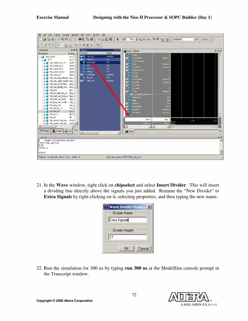
19. Now, add a few more signals of your own choosing to the Wave window:
From the design hierarchy browser in the Workspace window, open the DUT folder
inside the test_bench. Then highlight the_led_pio.
20. In the Objects window, select chipselect and out_port. Drag them into the waveform
window, placing them at the bottom of the list of signals (please see over). (Note: Hold
down Ctrl in order to grab multiple individual objects.)
Exercise Manual Designing with the Nios II Processor & SOPC Builder (Day 1)
Copyright © 2008 Altera Corporation A-MNL-NIIHW-EX-8-1-v1
72
21. In the Wave window, right click on chipselect and select Insert Divider. This will insert
a dividing line directly above the signals you just added. Rename the “New Divider” to
Extra Signals by right-clicking on it, selecting properties, and then typing the new name.
22. Run the simulation for 300 us by typing run 300 us at the ModelSim console prompt in
the Transcript window.
Exercise Manual Designing with the Nios II Processor & SOPC Builder (Day 1)
Copyright © 2008 Altera Corporation A-MNL-NIIHW-EX-8-1-v1
73
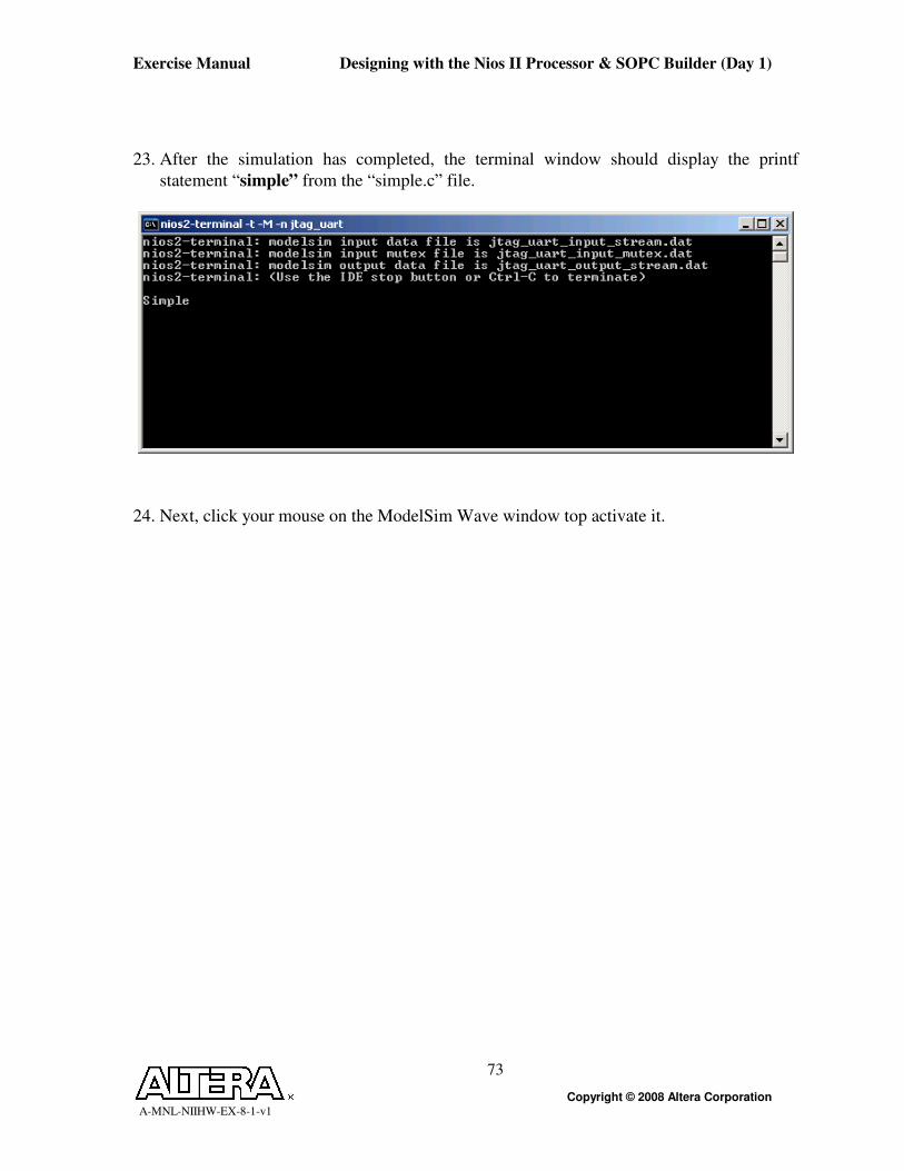
23. After the simulation has completed, the terminal window should display the printf
statement “simple” from the “simple.c” file.
24. Next, click your mouse on the ModelSim Wave window top activate it.
Exercise Manual Designing with the Nios II Processor & SOPC Builder (Day 1)
Copyright © 2008 Altera Corporation A-MNL-NIIHW-EX-8-1-v1
74
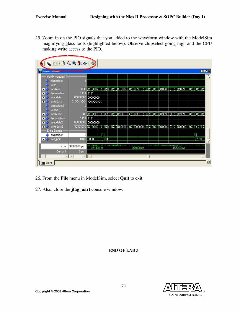
25. Zoom in on the PIO signals that you added to the waveform window with the ModelSim
magnifying glass tools (highlighted below). Observe chipselect going high and the CPU
making write access to the PIO.
26. From the File menu in ModelSim, select Quit to exit.
27. Also, close the jtag_uart console window.
END OF LAB 3

Exercise Manual Designing with the Nios II Processor & SOPC Builder (Day 1)
Copyright © 2008 Altera Corporation A-MNL-NIIHW-EX-8-1-v1
75
Lab 4
Adding a User Peripheral

Exercise Manual Designing with the Nios II Processor & SOPC Builder (Day 1)
Copyright © 2008 Altera Corporation A-MNL-NIIHW-EX-8-1-v1
76

Exercise Manual Designing with the Nios II Processor & SOPC Builder (Day 1)
Copyright © 2008 Altera Corporation A-MNL-NIIHW-EX-8-1-v1
77
In this lab you are going to add a user peripheral to your design and run some software to
test it. Additionally, if there is time, you will examine the hardware breakpoint and trace
capabilities of the FS2 Console in order to help you diagnose your software execution issues.
1. Return to SOPC Builder.
2. In the System Contents tab, uncheck the “Use” box next to the led_pio peripheral. You
will instead drive the LEDs from a PWM peripheral that you are about to import.
3. Open the Component Editor from the File menu by selecting New Component. Then
go to the HDL Files tab.
Click Add… HDL File and browse for “avalon_pwm.v” or “avalon_pwm.vhd”,
depending on which language you have chosen. Click Open. SOPC Builder will run the
Quartus II analyzer to verify whether there are any syntax errors in the code.
4. Once it completes, make sure that the Top Level Module points to avalon_pwm.
5. Go to the Signals tab and verify that the ports from the avalon_pwm module have
populated the Name column.
6. Next, you need to stitch the peripheral into the System Interconnect Fabric by mapping its
signals as shown below. Choose interface type “clock_reset” for signals clk and clr_n
and choose “conduit” for pwm_out. Make sure the signals are mapped to the Signal
Types shown.

Exercise Manual Designing with the Nios II Processor & SOPC Builder (Day 1)
Copyright © 2008 Altera Corporation A-MNL-NIIHW-EX-8-1-v1
78
7. Next, go to the Interfaces tab and rename the “conduit_end” type to “conduit”. (This is
not required, but the interface types can have any name you like, and “conduit” may be a
bit more meaningful to you than “conduit_end”.)
8. Go back to the Signals tab now, and set the pwm_out type to conduit to make sure it
picks up the name you just created.
9. Return again to the Interfaces tab, and press “Remove interfaces With No Signals” (if
necessary) to get rid of any residual interface types that you are not going to use.

Exercise Manual Designing with the Nios II Processor & SOPC Builder (Day 1)
Copyright © 2008 Altera Corporation A-MNL-NIIHW-EX-8-1-v1
79
10. Take a look at interface type “avalon_slave_0”. Set the Read Wait and Write Wait
values 0, and leave the other settings as default.
Exercise Manual Designing with the Nios II Processor & SOPC Builder (Day 1)
Copyright © 2008 Altera Corporation A-MNL-NIIHW-EX-8-1-v1
80
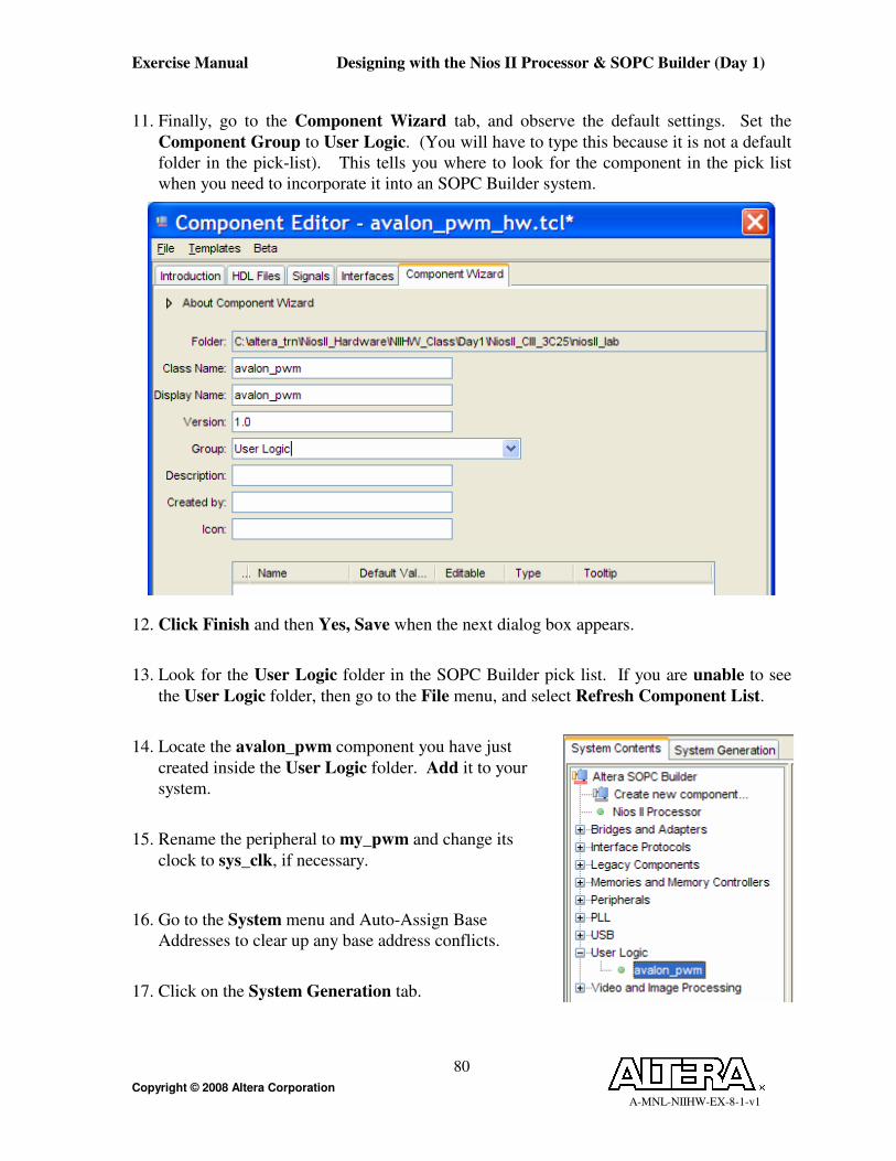
11. Finally, go to the Component Wizard tab, and observe the default settings. Set the
Component Group to User Logic. (You will have to type this because it is not a default
folder in the pick-list). This tells you where to look for the component in the pick list
when you need to incorporate it into an SOPC Builder system.
12. Click Finish and then Yes, Save when the next dialog box appears.
13. Look for the User Logic folder in the SOPC Builder pick list. If you are unable to see
the User Logic folder, then go to the File menu, and select Refresh Component List.
14. Locate the avalon_pwm component you have just
created inside the User Logic folder. Add it to your
system.
15. Rename the peripheral to my_pwm and change its
clock to sys_clk, if necessary.
16. Go to the System menu and Auto-Assign Base
Addresses to clear up any base address conflicts.
17. Click on the System Generation tab.
Exercise Manual Designing with the Nios II Processor & SOPC Builder (Day 1)
Copyright © 2008 Altera Corporation A-MNL-NIIHW-EX-8-1-v1
81
18. Save your system and then re-Generate.
19. Once the system has re-generated go to the schematic editor in Quartus II; select and
then right-click on the niosII symbol; and choose Update Symbol or Block.
(Observe how your changes have affected the ports on the symbol.)
20. Save the updated schematic. File => Save, and Compile the new design by clicking .
Click OK when compilation has completed successfully. (Note: Quartus II may ask you
to close the Block Editor – this means close SOPC Builder.)
21. Open the Quartus II Programmer by clicking on or by going to the Tools menu.
22. Check the Program / Configure box for niosII_lab.sof, and press Start to download the
new design to the development board.
23. Go back to the Nios II IDE, and create a new software project (File -> New->Project.)
Choose Nios II C/C++ Application, and press Next.
24. Pick the Blank Project template from the Select Project Template panel on the left
hand side of the window, and name the application niosII_pwm_project. Then specify
your ptf file, niosII.ptf, as the SOPC Builder System.
25. Click Finish.

Exercise Manual Designing with the Nios II Processor & SOPC Builder (Day 1)
Copyright © 2008 Altera Corporation A-MNL-NIIHW-EX-8-1-v1
82
26. Use Windows Explorer to drag pwm.c and the accompanying header file,
altera_avalon_pwm_regs.h, to the niosII_pwm_project folder in the Nios II IDE.
27. Right-click on niosII_pwm_project, and select Build Project and then Run in
Background.
28. After build completes right-click and select Run As-> Nios II Hardware.
Note:
If Run terminates before the code downloads to your board and you get a message that
you have “more than one JTAG cable available”, etc. then select Run > Run… Then,
from the Target Connection tab, choose your download cable, press Apply, and Run.

Exercise Manual Designing with the Nios II Processor & SOPC Builder (Day 1)
Copyright © 2008 Altera Corporation A-MNL-NIIHW-EX-8-1-v1
83
29. The message “Nios II PWM Lab” should now be seen in the Console Window in the
Nios II IDE followed by the question:
“Please enter an LED intensity between 1 to 4 (0 to exit)”.
30. Place your mouse underneath the text and then click to set the cursor, and adjust the
LED brightness by typing 1, 2, 3 or 4 followed by a carriage return, etc.
31. If you press 0 on your keyboard, it will terminate the program loop.

Exercise Manual Designing with the Nios II Processor & SOPC Builder (Day 1)
Copyright © 2008 Altera Corporation A-MNL-NIIHW-EX-8-1-v1
84
Optional Section:
Hardware Breakpoints and Trace
1. In the Nios II IDE, go to the Run menu and select Debug…. Then, go to the Debugger
tab, and check Use FS2 console window for trace and watchpoint support, select
Apply, and then select Debug.
2. After a few moments, the FS2 Console window will open and then minimize at the
bottom of your screen. Leave it there for now; you will open it again in a moment.

Exercise Manual Designing with the Nios II Processor & SOPC Builder (Day 1)
Copyright © 2008 Altera Corporation A-MNL-NIIHW-EX-8-1-v1
85
3. Go to the Memory tab in the Nios II IDE Debugger.
If the Memory window is not visible in the Nios
II IDE, then open it using Window > Show View
> Memory.
Note: The Memory window will open down in the
Console window near the bottom of the screen.
If you wish, you can drag it up to the top right of
the IDE as shown below, so that it sits in line
with the Variables and Registers windows or just
leave it at the bottom.

Exercise Manual Designing with the Nios II Processor & SOPC Builder (Day 1)
Copyright © 2008 Altera Corporation A-MNL-NIIHW-EX-8-1-v1
86
4. Add a memory monitor by clicking on the “+” sign on the Memory tab.
5. Type &rx_char in the dialog box that appears. Then select OK.
This is the variable that you will be monitoring.
6. Look at the Memory window and jot down the address of rx_char on a piece of paper.
It may differ from what is shown below (ie. 0x041FFF7C).
Exercise Manual Designing with the Nios II Processor & SOPC Builder (Day 1)
Copyright © 2008 Altera Corporation A-MNL-NIIHW-EX-8-1-v1
87
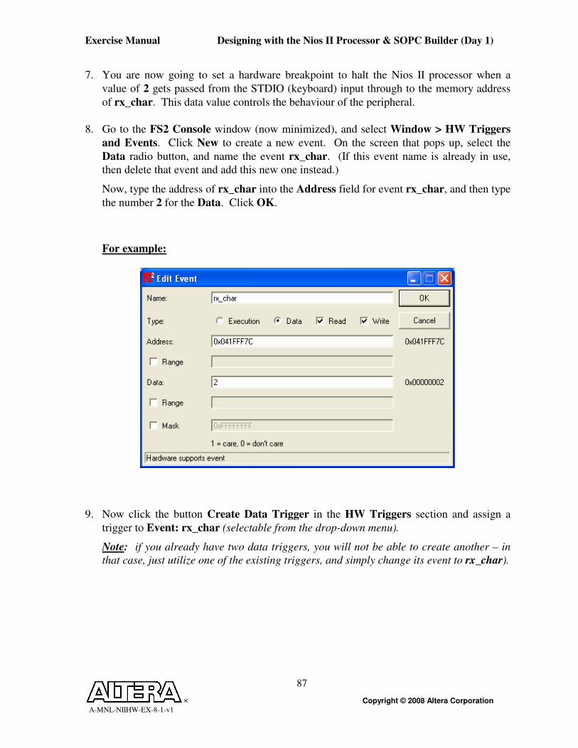
7. You are now going to set a hardware breakpoint to halt the Nios II processor when a
value of 2 gets passed from the STDIO (keyboard) input through to the memory address
of rx_char. This data value controls the behaviour of the peripheral.
8. Go to the FS2 Console window (now minimized), and select Window > HW Triggers
and Events. Click New to create a new event. On the screen that pops up, select the
Data radio button, and name the event rx_char. (If this event name is already in use,
then delete that event and add this new one instead.)
Now, type the address of rx_char into the Address field for event rx_char, and then type
the number 2 for the Data. Click OK.
For example:
9. Now click the button Create Data Trigger in the HW Triggers section and assign a
trigger to Event: rx_char (selectable from the drop-down menu).
Note: if you already have two data triggers, you will not be able to create another – in
that case, just utilize one of the existing triggers, and simply change its event to rx_char).

Exercise Manual Designing with the Nios II Processor & SOPC Builder (Day 1)
Copyright © 2008 Altera Corporation A-MNL-NIIHW-EX-8-1-v1
88
10. Finally, click the Action for Break Nios.
11. Now, open the HW Trace window from the FS2 Console. (Window > HW Trace).
This will show us 16 frames back worth of traced instructions. (Note: Access to deeper
trace is available via additional software keys purchased from FS/2.)
12. Go back to the Nios II IDE debugger, and select resume .
13. Then place the mouse under the text in the Nios II IDE debug Console window. Adjust
the LED brightness by typing the number 1 followed by Enter. Observe the LED’s
changing brightness.
14. Repeat for values 3 and 4.
15. Now, type 2 and Enter in the Nios II Console. (Note: This is the hardware break point
value!)
16. Observe that the FS2 Console window now displays “Trigger Breakpoint.”
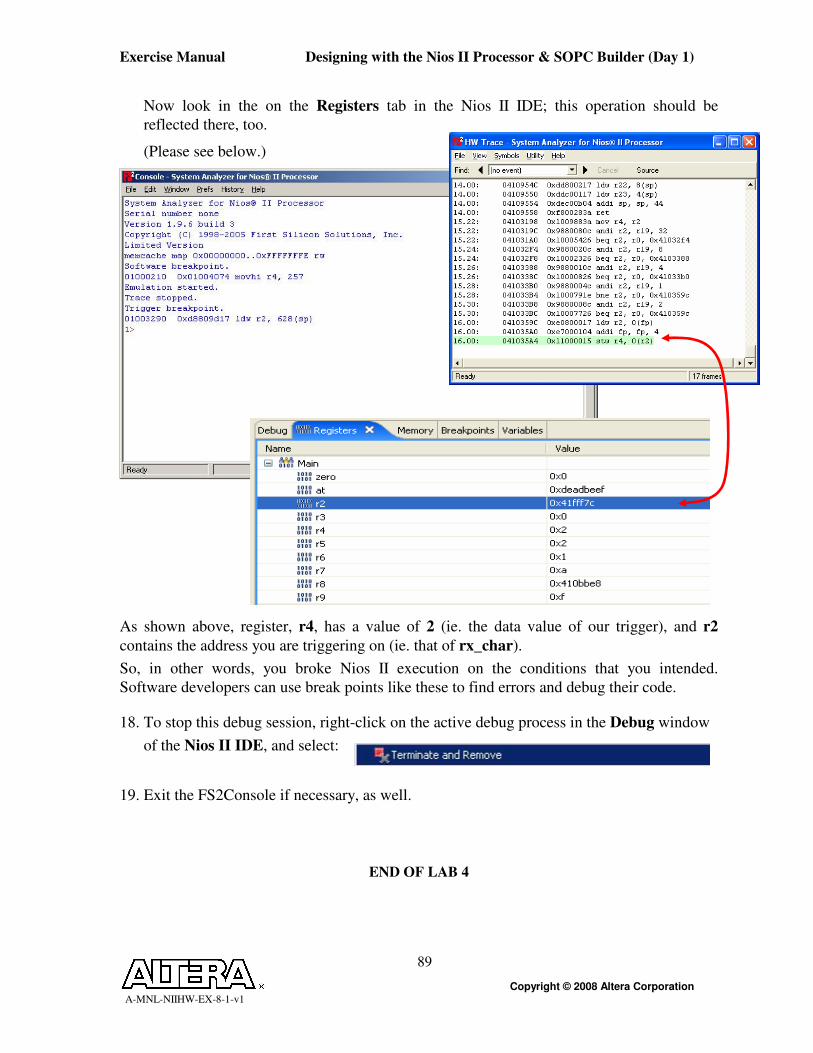
17. Observe the data trace window:
Notice that it now displays the instruction trace leading up to that breakpoint. Also, the
second instruction from the bottom should showsthe assembly command pass r4 to r2.
Exercise Manual Designing with the Nios II Processor & SOPC Builder (Day 1)
Copyright © 2008 Altera Corporation A-MNL-NIIHW-EX-8-1-v1
89
Now look in the on the Registers tab in the Nios II IDE; this operation should be
reflected there, too.
(Please see below.)
As shown above, register, r4, has a value of 2 (ie. the data value of our trigger), and r2
contains the address you are triggering on (ie. that of rx_char).
So, in other words, you broke Nios II execution on the conditions that you intended.
Software developers can use break points like these to find errors and debug their code.
18. To stop this debug session, right-click on the active debug process in the Debug window
of the Nios II IDE, and select:
19. Exit the FS2Console if necessary, as well.
END OF LAB 4

Exercise Manual Designing with the Nios II Processor & SOPC Builder (Day 1)
Copyright © 2008 Altera Corporation A-MNL-NIIHW-EX-8-1-v1
90
Exercise Manual Designing with the Nios II Processor & SOPC Builder (Day 1)
Copyright © 2008 Altera Corporation A-MNL-NIIHW-EX-8-1-v1
91
Lab 5
Custom Instructions

Exercise Manual Designing with the Nios II Processor & SOPC Builder (Day 1)
Copyright © 2008 Altera Corporation A-MNL-NIIHW-EX-8-1-v1
92

Exercise Manual Designing with the Nios II Processor & SOPC Builder (Day 1)
Copyright © 2008 Altera Corporation A-MNL-NIIHW-EX-8-1-v1
93
In this lab you will examine how you can boost the performance of a Nios II system without
having to increase the clock frequency by incorporating custom instructions and/or the DMA
controller peripheral.
First, you will look at the performance of a Nios II design before and after you add a custom
hardware instruction to the system. You will implement a CRC instruction which is an
algorithm used to detect whether or not data has been corrupted during transmission. It
detects a higher percentage of errors than a simple checksum.
The CRC calculation consists of an iterative algorithm involving XORs and shifts which
execute much faster in hardware than in software. Many algorithms besides the CRC
algorithm can achieve similar improvements by implementing the algorithm in hardware.
CRC is just one example.
After this, you will examine how you can off-load the CPU and prevent it from getting
bogged down by memory accesses which could otherwise be performed by a DMA controller.
1. Return to SOPC Builder Component Editor in order to edit the system. (You may have
to re-open this from Quartus II if you closed it in a previous step.)
2. Double-click on the cpu module that you have already instantiated in the SOPC Builder
System Contents page to re-open the cpu dialog box.
3. Then, select the Custom Instructions tab, and press Import...

Exercise Manual Designing with the Nios II Processor & SOPC Builder (Day 1)
Copyright © 2008 Altera Corporation A-MNL-NIIHW-EX-8-1-v1
94
4. The Component Editor will open. Go to the HDL files tab, and choose Add. Look for
the hardware file “crc_ci.v” for the crc custom instruction, and click Open.
5. Enter crc_ci for the Top Level Module if it is not already set.
6. On the Signals tab, ensure that the interface types for the remaining signals are set as
follows: (You may have to change the clk and reset signals to match.)
7. Now, go to the Interfaces tab, press Remove Interfaces with No Signals (if required),
and then find the nios_custom_instruction_slave_0 interface that you just created and
define its properties:
8. Ensure that the “Type” is set to “Custom Instruction Slave”.
9. Keep the rest of the defaults.
10. Select Finish and then Yes,
Save.

Exercise Manual Designing with the Nios II Processor & SOPC Builder (Day 1)
Copyright © 2008 Altera Corporation A-MNL-NIIHW-EX-8-1-v1
95
11. The crc_ci custom instruction should now be located in the library list. (If it does not
appear, press import again and then close it, and it should appear.)
12. Add it to your processor, and change its name to crc, as shown below.
13. Then press enter, and select Finish.
14. Now, click on the System Generation tab in SOPC Builder, and make sure the
Simulation check box is unchecked.
15. From the SOPC Builder File menu, Save the system (or type Ctrl-S).
16. Re-Generate the SOPC Builder system.
17. After system generation completes, it is good practice to update and save the symbol in
Quartus II by right-clicking on it in the schematic and selecting Update Symbol or
Block. (You should not see any changes to the symbol since the ports have not changed.)
Note: The ports on the symbol should not change. If they do, try closing SOPC Builder,
deleting the file crc_ci_hw.tcl file, and going through Steps 2-12 again. It is
possible that you entered a setting incorrectly in the Component Editor.
18. Save and then recompile the design by clicking . Once compilation completes, click
OK.
Exercise Manual Designing with the Nios II Processor & SOPC Builder (Day 1)
Copyright © 2008 Altera Corporation A-MNL-NIIHW-EX-8-1-v1
96
Re-Program the FPGA
1. Open the Quartus II programmer. Click on .
2. Tick the Program / Configure box. Click Start to download the design to the
development board.
Create Software Project to Test CRC Custom Instruction Against Software Execution
1. In the Nios II IDE, create a new project using a Blank Project template (File > New
Project > Nios II C/C++ Application), and name it crc_project. Then click Finish.
2. From Windows Explorer, drag the crc.c file (which is located in the software directory
in your design database) into the crc_project software application project folder in the
Nios II IDE.
3. If you are using a Cyclone III kit, also add the altera_avalon_pwm_regs.h file to the
project. (Since there is no seven segment display on these kits, you will flash the LEDs to
signify that the test has completed.)
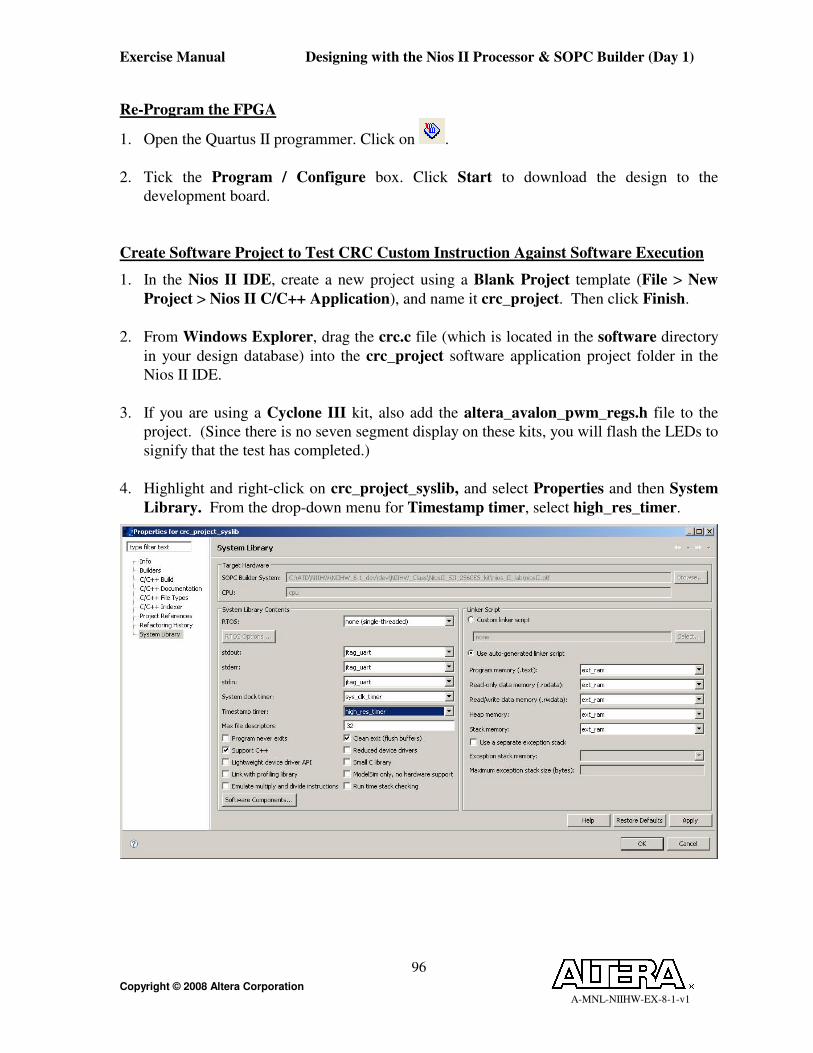
4. Highlight and right-click on crc_project_syslib, and select Properties and then System
Library. From the drop-down menu for Timestamp timer, select high_res_timer.

Exercise Manual Designing with the Nios II Processor & SOPC Builder (Day 1)
Copyright © 2008 Altera Corporation A-MNL-NIIHW-EX-8-1-v1
97
5. Then, go to the C/C++ Build page and then to the Nios II Compiler > General options
and select Optimization Level (-O3). Choose OK.
6. Now, highlight and right-click on crc_project and select Properties. Then, go to the
C/C++ Build page, and go to the Nios II Compiler General options area to again select
Optimization Level (-O3). Choose OK.

Exercise Manual Designing with the Nios II Processor & SOPC Builder (Day 1)
Copyright © 2008 Altera Corporation A-MNL-NIIHW-EX-8-1-v1
98
7. In the Nios II C/C++ Projects tab, Build the crc_project project. After the build has
completed, right click and select Run As > Nios II Hardware.
Note: If Run terminates before the code downloads to your board, and you get a message
that you have “more than one JTAG cable available”, etc. then select Run > Run… and
from the Target Connection tab choose the appropriate download cable and hit Apply
and Run.
8. Record the time taken to execute the crc routine 80 (hex) times.
Software CRC for Data Block = 0xbb88.
CPU time(ms): __________
Hardware CRC for Data Block = 0xbb88.
CPU time(ms): __________
9. Press the red “stop” button located above the Terminal Window to terminate the
program.

Exercise Manual Designing with the Nios II Processor & SOPC Builder (Day 1)
Copyright © 2008 Altera Corporation A-MNL-NIIHW-EX-8-1-v1
99
Optional Section:
DMA – Direct Memory Access
In this optional section, you are going to add a crc custom peripheral to our design and then
run some code that also takes advantage of the DMA controller in our system. The DMA
controller pumps data directly into the CRC peripheral for it to work on. You’ll see that this
is another way to achieve dramatic performance speed-up over just running software code.
1. In SOPC Builder, add the crc_peripheral.v (or crc_peripheral.vhd component,
depending on which language you have chosen) using the New Component Editor.
Adjust the port mappings in the event that they differ from what is shown below: (Note:
use the Component Editor, using the same procedure from Lab 3.)
Exercise Manual Designing with the Nios II Processor & SOPC Builder (Day 1)
Copyright © 2008 Altera Corporation A-MNL-NIIHW-EX-8-1-v1
100
2. On the interfaces tab, Remove Interfaces With No Signals, if necessary, and set the
Read and Write delays to 0 ns.
3. Go to the Component Wizard tab, and select “User Logic” for Component Group.
4. Then, select Finish and Yes, Save.
5. Locate the crc_peripheral in the User Logic folder in the SOPC Builder component pick
list, and Add it to your system. Then, rename the peripheral crc_periph, and ensure that
its clock domain is set to sys_clk.
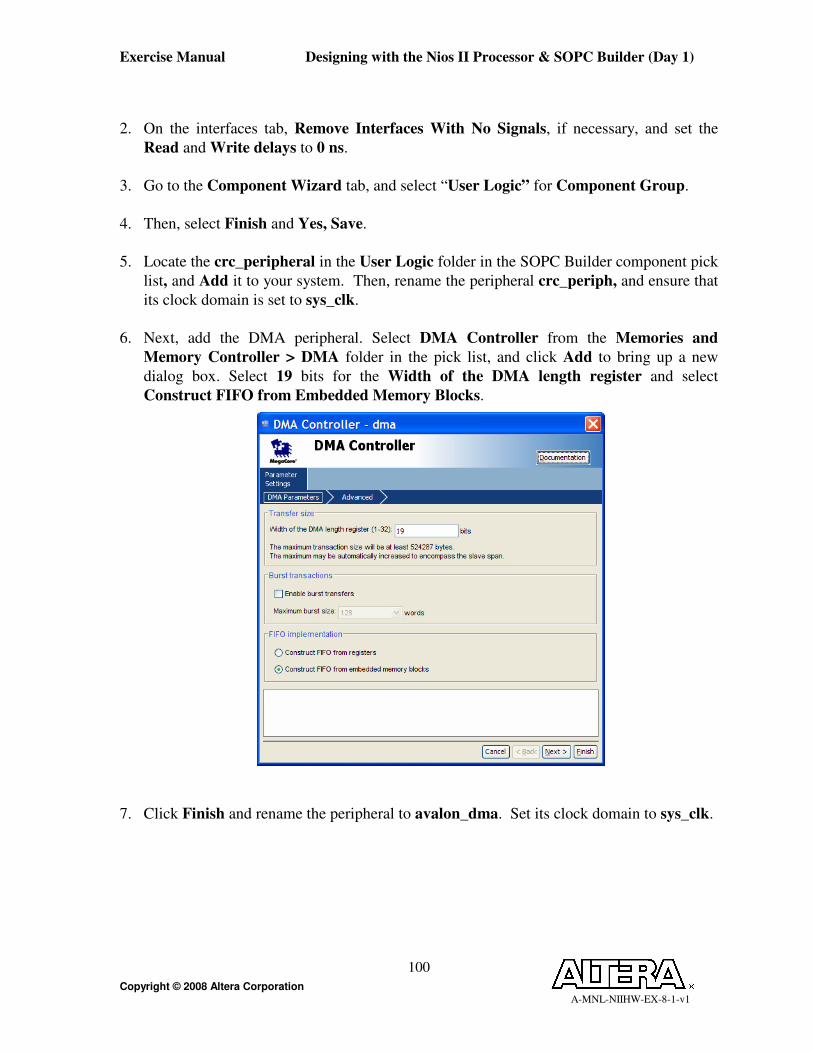
6. Next, add the DMA peripheral. Select DMA Controller from the Memories and
Memory Controller > DMA folder in the pick list, and click Add to bring up a new
dialog box. Select 19 bits for the Width of the DMA length register and select
Construct FIFO from Embedded Memory Blocks.
7. Click Finish and rename the peripheral to avalon_dma. Set its clock domain to sys_clk.

Exercise Manual Designing with the Nios II Processor & SOPC Builder (Day 1)
Copyright © 2008 Altera Corporation A-MNL-NIIHW-EX-8-1-v1
101
8. Connect the avalon_dma “read_master” and “write_master” ports to the crc_periph
and ext_ram_bus peripherals as shown below. This will give the DMA peripheral read
and write access to these peripherals.
Note: Simply hover the mouse over the interconnection to show the master-slave
interconnectivity and then click on the dots to connect or disconnect. Click Next.
9. Save, then re-Generate the system in the SOPC Builder.
10. Then re-compile the FPGA design in Quartus II . (Note: Be sure to Update Symbol
or Block first!)
11. After compilation completes, click OK and then open the Programmer . Select file
niosII_lab.sof and click Start to program the board with the new image.

Exercise Manual Designing with the Nios II Processor & SOPC Builder (Day 1)
Copyright © 2008 Altera Corporation A-MNL-NIIHW-EX-8-1-v1
102
12. In the Nios II IDE, create a new software project (File > New Project > Nios II C/C++
Application) based on a Blank Project template, and call it crcdma_project. Click
Finish to create the project.
13. Drag the crcdma.c file from the software directory in your design database into the
crcdma_project folder in the Nios II IDE using Windows Explorer.
14. If you are using a Cyclone III kit, also add the altera_avalon_pwm_regs.h file to the
project. (Since there is no seven segment display on these kits, you will flash the LEDs to
signify that the test has completed.)
15. In the Nios II C/C++ Projects tab, highlight and right-click on crcdma_project_syslib,
and select System Library. From the drop-down menu for Timestamp timer, select
high_res_timer.
16. Now, go to the C/C++ Build tab and select Optimization Level (-O3) from the General
Nios II IDE compiler options. Choose OK.
17. Now, highlight and right-click on crcdma_project, select the C/C++ Build tab and again
select Optimization Level (-O3) from the Nios II IDE General compiler options.
Choose OK.
18. In the Nios II C/C++ Projects tab, highlight the crcdma_project, and then right-click
and select Build Project. After the build has completed, right click and select Run As >
Nios II Hardware.
Note: If Run terminates before the code downloads to your board, and you get a message
that you have “more than one JTAG cable available”, etc. then select Run > Run… and
from the Target Connection tab choose the appropriate download cable and hit Apply
and Run.
19. Note the time taken to execute the crc function. Note the dramatic performance boost vs
running the crc algorithm out of software and the substantial performance boost over
running with a custom instruction alone. Clearly, the DMA controller was able to
effectively off-load the CPU and thereby enhance system performance.
CPU time: __________________
END OF LAB 5
Exercise Manual Designing with the Nios II Processor & SOPC Builder (Day 1)
Copyright © 2008 Altera Corporation A-MNL-NIIHW-EX-8-1-v1
103
Lab 6
Flash Programmer

Exercise Manual Designing with the Nios II Processor & SOPC Builder (Day 1)
Copyright © 2008 Altera Corporation A-MNL-NIIHW-EX-8-1-v1
104

Exercise Manual Designing with the Nios II Processor & SOPC Builder (Day 1)
Copyright © 2008 Altera Corporation A-MNL-NIIHW-EX-8-1-v1
105
You will now demonstrate how easy it is to download the FPGA hardware and software
images to Flash using the Nios II Flash Programmer tool. The one proviso is that you need
to have a design loaded on the FPGA that has a Nios II Processor in it along with a CFI
flash peripheral. You can use the hardware from your labs today for the purpose of running
the flash programmer. (If you are using a Cyclone III kit, you also have the option of using
the hardware image stored in the Flash_files folder provided with your project.)
1. Press the red “stop” button above the Terminal Window in the Nios II IDE to
Terminate the current process
2. If you are using a Cyclone III Kit, skip directly to Option 2 (located a few pages hence);
otherwise proceed to Option 1 below.
For all kits other than those with a Cyclone III FPGA, use the following procedure:
1. You will now program the flash memory with the crcci_project software code and a
hardware design that you recently used. Go to the Tools menu, and select Flash
Programmer.
2. Click on Flash Programmer and then select the New launch configuration button (as
shown below), and then browse to the crc_project (ie. the crc_project.elf file generated
during the Build process).
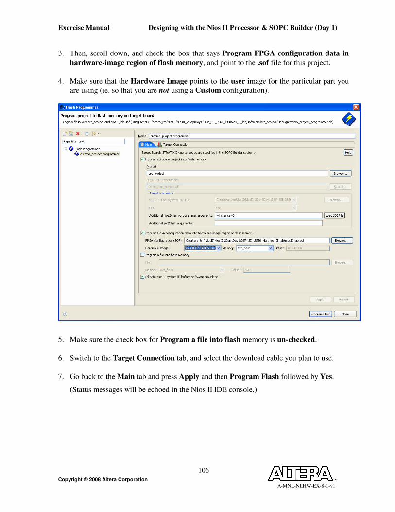
Exercise Manual Designing with the Nios II Processor & SOPC Builder (Day 1)
Copyright © 2008 Altera Corporation A-MNL-NIIHW-EX-8-1-v1
106
3. Then, scroll down, and check the box that says Program FPGA configuration data in
hardware-image region of flash memory, and point to the .sof file for this project.
4. Make sure that the Hardware Image points to the user image for the particular part you
are using (ie. so that you are not using a Custom configuration).
5. Make sure the check box for Program a file into flash memory is un-checked.
6. Switch to the Target Connection tab, and select the download cable you plan to use.
7. Go back to the Main tab and press Apply and then Program Flash followed by Yes.
(Status messages will be echoed in the Nios II IDE console.)

Exercise Manual Designing with the Nios II Processor & SOPC Builder (Day 1)
Copyright © 2008 Altera Corporation A-MNL-NIIHW-EX-8-1-v1
107
8. It may take a couple of minutes to program the flash, depending on your device.
9. After programming is complete, press the Power-On Reset button (or “Reset Config”,
depending on your board) located near the top of the development board to transfer the
hardware image from flash into the FPGA. If nothing happens, press the CPU reset
button.
10. Now, observe the program running out of flash. (ie. The seven segment display should
increment from “00” up to “80”.)
11. Now, return to the Nios II Command Shell (re-open if you closed it). At the shell
prompt, type: nios2-terminal. This will allow you to catch and view the printf’s from
the Nios II processor while running from flash.
12. Press the CPU Reset button on the board to run the program again. The program should
only take a little over a second to run. You should see the messages spool to the Nios II
console and observe the seven segment display change again.
Note: The CRC value will probably have changed because the contents of flash (ie. that are
being CRC’d) have changed.
13. Press Ctrl-C in the Nios II Command Shell to end the terminal session.

Exercise Manual Designing with the Nios II Processor & SOPC Builder (Day 1)
Copyright © 2008 Altera Corporation A-MNL-NIIHW-EX-8-1-v1
108
If you are using one of the Cyclone III kits, use the following procedure instead:
1. Go to the Start menu and select:
Program > altera > Nios II EDS 8.0 > Nios II 8.0 Command Shell.
2. Change directory to your hardware project folder using the cd command:
cd C:\altera_trn\NiosII_HW\NiosII_2Day\NiosII_CIII_3C25\niosII_lab
Note: You can accelerate this process and avoid typing the full path yourself by typing
cd “ in the console window and then dragging and dropping the path from your
windows explorer browser to the Command Shell and then closing the quote by
typing another ”. This might save you some time and is a good trick to
remember.
3. Then type the following commands to erase the flash on your board, create a flash image
out of your hardware (.sof) file, and then program the flash chip with the hardware image.
Note: You must use the Command Shell to program the hardware image for the Cyclone
III kits in because there is currently no way to accommodate the active parallel
flash loading process used on the Cyclone III boards through the Quartus II 8.0
Nios II Flash Programmer GUI.
To erase the flash, type the following (please note the base address of the flash
component in your SOPC Builder system and insert it into the following command):
nios2-flash-programmer --base=<flash base address> --erase-all
eg. nios2-flash-programmer --base=0x4000000 –erase-all
To create the flash file, type:
sof2flash --activeparallel --offset=0x20000 --input=niosII_lab.sof --output=hardware_image.flash
To program “hardware_image.flash” to flash, please again note the base address of
the flash component in your system and insert it into the following command:
nios2-flash-programmer --base=<flash base address> hardware_image.flash
eg. nios2-flash-programmer --base=0x4000000 hardware_image.flash

Exercise Manual Designing with the Nios II Processor & SOPC Builder (Day 1)
Copyright © 2008 Altera Corporation A-MNL-NIIHW-EX-8-1-v1
109
4. After the hardware image has been flashed, open the Nios II Flash Programmer GUI in
the Nios II IDE so that you can program the software image to flash. In the Nios II IDE,
open the Tools menu, and select Flash Programmer.
5. Click on Flash Programmer and then select the New launch configuration button.
6. Then browse to crcci_project in the Project field (ie. the crcci_project.elf file generated
during the Build process). This is the software image we will program to flash.
7. Make sure the check boxes for the Program FPGA configuration data into hardware-
image region of flash and Program a file into flash memory switches are un-checked.
8. Switch to the Target Connection tab, and select the download cable you plan to use.
9. Go back to the Main tab and press Apply and then Program Flash followed by Yes.
(Status messages will be echoed in the Nios II IDE console.)
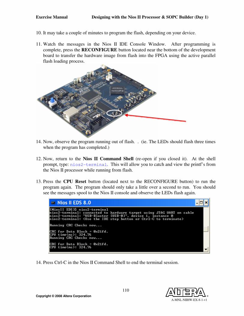
Exercise Manual Designing with the Nios II Processor & SOPC Builder (Day 1)
Copyright © 2008 Altera Corporation A-MNL-NIIHW-EX-8-1-v1
110
10. It may take a couple of minutes to program the flash, depending on your device.
11. Watch the messages in the Nios II IDE Console Window. After programming is
complete, press the RECONFIGURE button located near the bottom of the development
board to transfer the hardware image from flash into the FPGA using the active parallel
flash loading process.
14. Now, observe the program running out of flash. . (ie. The LEDs should flash three times
when the program has completed.)
12. Now, return to the Nios II Command Shell (re-open if you closed it). At the shell
prompt, type: nios2-terminal. This will allow you to catch and view the printf’s from
the Nios II processor while running from flash.
13. Press the CPU Reset button (located next to the RECONFIGURE button) to run the
program again. The program should only take a little over a second to run. You should
see the messages spool to the Nios II console and observe the LEDs flash again.
14. Press Ctrl-C in the Nios II Command Shell to end the terminal session.

Exercise Manual Designing with the Nios II Processor & SOPC Builder (Day 1)
Copyright © 2008 Altera Corporation A-MNL-NIIHW-EX-8-1-v1
111
15. If you are using a Nios II Evaluation (NEEK) Kit, then please re-program flash to
restore the original demonstration design (see steps below).
To Recover the Factory Image on the NEEK Boards:
i) Within the Nios II Command Shell, change directory into the “Flash_files” folder:
cd Flash_files
ii) Then type:
nios2-flash-programmer --base=<flash base address> restore_cycloneIII_3c25.flash
Eg.
nios2-flash-programmer --base=0x4000000 restore_cycloneIII_3c25.flash
iii) Once the command completes, press the “RECONFIGURE” button located near the
bottom of the development board to reset the FPGA with the factory image.
iv) Check that the Application Selector utility is up and running again on the LCD
panel.
Note: if these commands do not respond, then you may need to reprogram the FPGA with
a valid hardware image first in order to carry out the flash image transfer.
16. Close SOPC Builder (File > Exit).
17. Exit Quartus II (File > Exit).
18. Exit the Nios II IDE (File > Exit).
END OF LAB 6