Embed Size (px)
Citation preview

Application ReportSPRAAB3–July 2005
Designing a TMS320F280x Based Digitally ControlledDC-DC Switching Power Supply
Shamim Choudhury .......................................... Digital Power, C2000 DSP and System Power Management
ABSTRACT
This application report presents a TMS320F280x based digital control design andimplementation of a high frequency dc-dc switching power supply. Starting with a dc-dcbuck converter and a given set of performance specifications, different control blocksand parameters, used as in the analog control design approach, are reviewed prior tothe control design in digital domain. The control loop is then analyzed and the digitalcontrollers are designed using different control design approaches. Code examples areprovided illustrating the controller implementation using TMS320F280x DSP controller.MATLAB based digital control design approaches presented here are finally validatedwith multiple test results from a prototype converter.
Contents1 Introduction .......................................................................................... 22 Digital Control Implementation for DC-DC Converter.......................................... 23 Conclusion ......................................................................................... 144 References......................................................................................... 15
List of Figures
1 DSP based Digital Control of DC-DC Converter ............................................... 22 DC-DC Converter Digital Control Loop Sampling Scheme ................................... 33 DC-DC Converter Control Loop Block Diagram in s-domain ................................. 44 DC-DC Converter Control Loop Bode Plot Gp(s) * Gc1(s)*Kd*Fm (MATLAB) ............. 55 DC-DC Converter Load Transient Response (loop gain = Gp*Gc1*Fm*Kd) ............... 66 DC-DC Converter Digital Control Loop Block Diagram........................................ 77 Sample and Hold Process in a Digital System ................................................. 78 DC-DC Converter Digital Control Loop Bode Plot Gp1*Gc2 (MATLAB) .................... 89 DC-DC Converter Digital Control Loop Bode Plot Gp2*Gc2 (MATLAB) .................... 910 DC-DC Converter Control Loop Bode Plot Gp2*Gc2 (Test result from prototype
h/w) ................................................................................................. 1011 DC-DC Converter Load Transient Response (Loop gain = Gp2*Gc2) .................... 1112 DC-DC Converter Digital Control Loop Bode Plot Gp3*Gc2 (MATLAB)................... 1213 DC-DC Converter Digital Control Loop Bode Plot Gp3*Gc3 (MATLAB)................... 1314 DC-DC Converter Load Transient Response (Loop gain = Gp3*Gc3) .................... 1315 DC-DC Converter Load Transient Response (Loop gain = Gp3*Gc3)..................... 14
SPRAAB3–July 2005 Designing a TMS320F280x Based Digitally Controlled DC-DC Switching Power Supply 1

www.ti.com
1 Introduction
2 Digital Control Implementation for DC-DC Converter
Vin
Iin
GateDrive
Q1
Gp
PWM1d
C
RC
RL
Gc(z)
SignalConditioning
A/D
Kd
Vref
U E
Vout
TMS320F280x
Vos
Vo
L
Introduction
Digital control of switching power supplies is becoming more and more common in industry today becauseof the availability of low cost, high performance DSP controller with enhanced and integrated powerelectronic peripherals such as analog-to-digital (A/D) converters and pulse width modulator (PWM).
DSP based digital control allows for the implementation of more functional control schemes, standardcontrol hardware design for multiple platforms and flexibility of quick design modifications to meet specificcustomer needs. Digital controllers are less susceptible to aging and environmental variations and havebetter noise immunity. Modern 32-bit DSP controllers, such as TMS320F280x, with processor speed up to100MHz and enhanced peripherals such as, high resolution PWM module, 12-bit A/D converter withconversion speed up to 160nSec, 32x32-bit multiplier, 32-bit timers and real-time code debuggingcapability, gives the power supply designers all the benefits of digital control and allows implementation ofhigh bandwidth, high frequency power supplies without sacrificing performance [1-4]. The extra computingpower of such processors also allows implementation of sophisticated nonlinear control algorithms,integrate multiple converter control into the same processor and optimize the total system cost. However,the power supply engineers, mostly familiar with analog control design, are faced with new challenges asthey start to adopt these digital control techniques in their designs.
Since DSPs just started to gain some serious considerations in controlling power supplies, many pertinentfactors in the design and implementation of a digital control loop need to be addressed. Accuraterepresentation of the control blocks and the associated control parameters is critical for the analogdesigners in order to enable them to implement the DSP based digital control techniques using thewell-known analog control design approaches. This application report, therefore, describes a step-by-stepDSP based digital control design and implementation of a high frequency dc-dc converter. Starting with adc-dc buck converter and a given set of performance specification, it discusses different control blocks,different control design approaches and highlights the significant differences in designing control in thedigital domain compared to the analog approach. Two approaches to the digital control design areillustrated namely, the design by emulation and the direct digital design. These are first shown in MATLABand then verified by experimental results. In this process the effects of sampling delay and thecomputation delay are also analyzed in MATLAB and then verified experimentally. Finally the assemblycode listings implementing the designed controllers are provided in order to aid the users quickly validatethese controllers using a similar DSP controlled dc-dc converter set up.
Figure 1 shows a simplified block diagram of a digitally controlled dc-dc converter interfaced to aTMS320F280x DSP controller.
Figure 1. DSP based Digital Control of DC-DC Converter
Designing a TMS320F280x Based Digitally Controlled DC-DC Switching Power Supply2 SPRAAB3–July 2005

www.ti.com
2.1 Digital Sampling Loop Implementation
CodeExecution
Context Save
Context RestoreExecute Controller
Background loop
Spare
Interrupt Interrupt
ISR
T1
t
n+1Sampling Scheme 1
Td = 0.5Ts
Tadc Tadc
UpdateDuty
StartADC
Write Compare
TSTS
TdUpdate
DutyTd
StartADC
Sampling period NN+1
PWM period n
Write Compare
Digital Control Implementation for DC-DC Converter
As indicated in Figure 1, a single signal measurement is needed to implement the voltage mode control ofthe dc-dc converter. The instantaneous output voltage Vout is sensed and conditioned by the voltagesense circuit and then input to the DSP via the ADC channel. The digitized sensed output voltage Vo iscompared to the reference Vref. The voltage loop controller Gc is designed to make the output voltageVout track the reference Vref and at the same time achieve the desired dynamic performance. Thedigitized output U of this controller provides the duty ratio command for the buck regulator switch Q1. Thiscommand output is used to calculate the appropriate values for the timer compare registers in the on-chipPWM module. The PWM module uses this value to generate the PWM output, PWM1 in this case, thatfinally drives the buck converter switch Q1.
Figure 2 shows one example of a digital sampling scheme using the DSP on-chip peripherals.
Figure 2. DC-DC Converter Digital Control Loop Sampling Scheme
The sampling scheme affects the digital controller design and, therefore, needs appropriate attention.PWM output frequency is set up by configuring one of the on-chip Timers, T1 in this case. In this example,T1 generates a dual edge modulated (symmetric), 250 kHz PWM output. These timers have associatedcompare registers which are used to write the calculated duty ratio values. These values then getcompared with the timer counter value in order to generate the PWM output. The time at which a newlywritten compare value affects the actual PWM output duty ratio is controlled by associated PWM controlregisters. In this example, the PWM control registers are set up such that a new value written in thecompare register, changes the actual PWM output duty ratio at the start of the subsequent timer (T1)period. Also, the ADC control registers are set up such that the AD conversion is triggered at the middle ofthe ON pulse of the PWM output. As soon as the conversion is complete, the ADC module is set up togenerate an interrupt. The time delay between the start of AD conversion and this interrupt is shown inFigure 2, as Tadc. This time includes the AD conversion time and the processor interrupt latency. Insidethe interrupt service routine (ISR), the user software reads the converted value from the ADC resultregister, implements the controller and then writes the new PWM duty ratio value to the appropriate PWMcompare register. However, this new duty ratio value takes affect at the start of the subsequent PWMcycle. From Figure 2, it is clear that the time delay Td, between the ADC sampling instant and the PWMduty ratio update, is half the PWM period. In this case, the PWM period and the sampling period (Ts) areequal and so the computation delay is, Td = Ts/2. Also shown in Figure 2, the calculation of a new dutyratio value inside the ISR is completed well before a subsequent interrupt is generated. This means that,at this sampling frequency, the processor bandwidth (100 MHz) allows for sufficient spare time to extendthe ISR and execute multiple controllers or other time critical tasks. Some of this spare time can also beused for non-time critical tasks by running them from a background loop.
SPRAAB3–July 2005 Designing a TMS320F280x Based Digitally Controlled DC-DC Switching Power Supply 3

www.ti.com
2.2 DC-DC Controller Design
d
U
Gp(s)
E
Vo
Fm Kd
Vref
Gc(s)
U(n) E(n)Gc(z)
Vo
GP(S) � Vin
�sRCC�1�
�s2LC�1� RCRL��s�RCC� L
RL��1�
�(3.24 � 10�5s � 5.0)
(1.685 � 10�9s2 � 1.648 � 10�5s � 1.0)
Digital Control Implementation for DC-DC Converter
The system parameters used in this design are:
• Vin = 4~6V, Vout = 1.6V, Max output current Iout = 16A, RL = Vout/Iout = 0.1 ohm (Minimum)• Maximum output voltage (used for ADC signal scaling) Vomax = 2V• PWM frequency fpwm = 250kHz; Voltage loop sampling frequency fs = 250kHz• Output filter components, L = 1.0uH, C = 1620uF, RC = 0.004 Ohm• Desired voltage loop bandwidth fcv = 20kHz• Phase Margin = 45 deg, Settling time < 75uSec
In order to design the digital controller, two approaches are discussed. These are, 1. Design by Emulationand 2. Direct Digital Design.
2.2.1 Design by Emulation
This is also known as Digital Redesign Approach. In this method, an analog controller is first designed inthe continuous domain as if one were building continuous time control system, by ignoring the effects ofsampling and hold associated with the AD converter and the digital PWM circuits. The analog controller isthen converted to a discrete-time compensator by some approximate techniques. Figure 3 represents asimplified block diagram of the system in Figure 1. It shows all the different components of this closed loopcontrol system in s-domain.
Figure 3. DC-DC Converter Control Loop Block Diagram in s-domain
The small signal power stage model of the buck converter in s-domain is indicated as Gp(s). For the givensystem parameters with Vin = 5.0V and RL = 0.1 ohm, this is derived as,
If the maximum output voltage is Vomax, then the voltage feedback factor is, Kd = 1/Vomax, provided thatthe digital output voltage Vo is represented in Q31 fixed-point format for this 32-bit DSP controller [6]. ThePWM modulator gain is Fm = 1. This is so because the user software together with the on-chip PWMhardware can be configured such that as the controller output U (in Q31) varies between 0 ~ 7FFFFFFFh,the PWM output duty ratio d varies between 0 ~ 1, [6].
Now for this plant Gp(s), a suitable analog controller Gc(s) is designed in MATLAB using the availablecontrol design tool called ‘sisotool’. The Bode plot for this design is shown in Figure 4 where the systembandwidth (BW) is set at 25 kHz with a phase margin (PM) of 71 deg.
Designing a TMS320F280x Based Digitally Controlled DC-DC Switching Power Supply4 SPRAAB3–July 2005

www.ti.com
GC1(s)�(14.3s2� 6.514� 105s� 7.2� 109)
s(s� 1.256� 105)
Gc1_s � tf��14.3 6.514e005 7.2e009�, [1 1.256e005 0]�; %Controller in s−domain%Gc1_z � c2d(Gc1_s, Ts, �matched�); % Digital Controller %
GC1(z)� UE�
12.34� 22.53z�1� 10.28z12
1� 1.605z�1�0.6051z�2
U(n)� 1.605U(n� 1)� 0.605U(n� 2)�12.34E(n)� 22.53E(n� 1)�10.28E(n� 2)
Digital Control Implementation for DC-DC Converter
Figure 4. DC-DC Converter Control Loop Bode Plot Gp(s) * Gc1(s)*Kd*Fm (MATLAB)
The corresponding controller Gc1(s) can be easily imported from the MATLAB control design toolbox. Thisis found as,
This analog controller Gc1(s) can be discretized by any of the commonly used discretization methodssuch as, Bilinear, Pole-Zero match and Forward etc. [5, 9]. This can be performed in MATLAB simply bywriting the MATLAB script as:
This generates the following digital controller Gc1(z):
where, the sampling time is Ts = 1/fs = 4uSec. In discrete form, this controller is written as,
where, U is the control output and E is the error voltage. The quantities with (n) denote the sampledvalues for the current sampling cycle, the quantities with (n-1) denote one sample old values and so on.
SPRAAB3–July 2005 Designing a TMS320F280x Based Digitally Controlled DC-DC Switching Power Supply 5

www.ti.com
Digital Control Implementation for DC-DC Converter
This controller was implemented using the TMS320F280x DSP instruction set. During the codeinitialization the coefficients of the above controller are first converted to a suitable fixed point format (Qformat) in order to get the best accuracy out of this 32-bit processor. An example code listing is given inthe zip file for a similar controller. The fixed point format used for the controller coefficients in this codeexample is Q26.
Once the controller was implemented in the DSP, its closed loop dynamic performance was tested on aprototype dc-dc converter. This transient load response is shown in Figure 5:
Figure 5. DC-DC Converter Load Transient Response (loop gain = Gp*Gc1*Fm*Kd)
For a step load change of 15A, the output voltage settles within 30uSec (1% band). The converter has asatisfactory time response. However, the damping of the transient response does not reflect a phasemargin of 71 deg as shown in MATLAB Bode plot (see Figure 4). This difference in the designed andactual phase margin is because of the fact that we completely ignored the effect of sampling and hold andthe computation delay. In digital control design the effect of these delays can be taken into account priorto the control design that results in a more predictable and accurate dynamic performance. This isillustrated next.
Designing a TMS320F280x Based Digitally Controlled DC-DC Switching Power Supply6 SPRAAB3–July 2005
www.ti.com
d
U(n)
Gp(s)
E(n)Vref
ZOH Kd
−Gc(z)
Hc Ts
+
Vout
Gp(z)
Vo(n)
Ts
Time DelayTS2
�ZOH � � �
Ts2
� � 180ffs
SH(s) �(1 � e�STs)
s
Digital Control Implementation for DC-DC Converter
2.2.2 Direct Digital Design
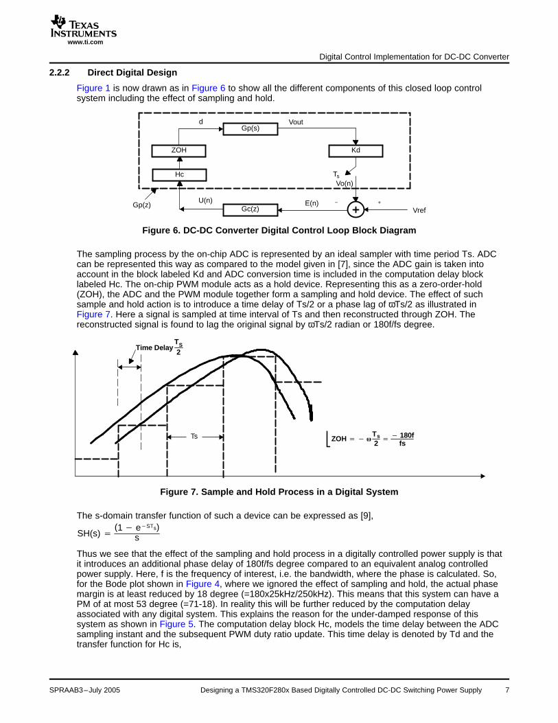
Figure 1 is now drawn as in Figure 6 to show all the different components of this closed loop controlsystem including the effect of sampling and hold.
Figure 6. DC-DC Converter Digital Control Loop Block Diagram
The sampling process by the on-chip ADC is represented by an ideal sampler with time period Ts. ADCcan be represented this way as compared to the model given in [7], since the ADC gain is taken intoaccount in the block labeled Kd and ADC conversion time is included in the computation delay blocklabeled Hc. The on-chip PWM module acts as a hold device. Representing this as a zero-order-hold(ZOH), the ADC and the PWM module together form a sampling and hold device. The effect of suchsample and hold action is to introduce a time delay of Ts/2 or a phase lag of ωTs/2 as illustrated inFigure 7. Here a signal is sampled at time interval of Ts and then reconstructed through ZOH. Thereconstructed signal is found to lag the original signal by ωTs/2 radian or 180f/fs degree.
Figure 7. Sample and Hold Process in a Digital System
The s-domain transfer function of such a device can be expressed as [9],
Thus we see that the effect of the sampling and hold process in a digitally controlled power supply is thatit introduces an additional phase delay of 180f/fs degree compared to an equivalent analog controlledpower supply. Here, f is the frequency of interest, i.e. the bandwidth, where the phase is calculated. So,for the Bode plot shown in Figure 4, where we ignored the effect of sampling and hold, the actual phasemargin is at least reduced by 18 degree (=180x25kHz/250kHz). This means that this system can have aPM of at most 53 degree (=71-18). In reality this will be further reduced by the computation delayassociated with any digital system. This explains the reason for the under-damped response of thissystem as shown in Figure 5. The computation delay block Hc, models the time delay between the ADCsampling instant and the subsequent PWM duty ratio update. This time delay is denoted by Td and thetransfer function for Hc is,
SPRAAB3–July 2005 Designing a TMS320F280x Based Digitally Controlled DC-DC Switching Power Supply 7
www.ti.com
HC(s) � e�STd
GP(z) � Z�1s �1 � e�STs�.HC(s).GP(s).Kd�
GP1(Z)� 0.0494(z� 0.5283)
(z2� 1.952z� 0.962)
Discrete System Bode PlotGp1(z)*Gc2(z)
(Td = 0)
BW = 27.9kHz, PM = 61.6 deg, GM = 9dB
GC2(z)� UE�
14.87� 26.91z�1� 12.16z�2
1� 1.473z�1� 0.473z�2
Digital Control Implementation for DC-DC Converter
In direct digital design approach, the continuous time power stage model is first discretized with ZOH andthe sampler. Once this is available, the discrete-time compensator. i.e., a digital controller Gc(z) isdesigned directly in the z-domain using methods similar to the continuous-time frequency responsemethods. This has the advantage that the poles and zeros of the digital controllers are located directly,resulting in a better load transient response, as well as better phase margin and bandwidth for the closedloop power converter. The discrete-time transfer function Gp(z) of the converter plant, including the ZOH,the sampler, the voltage sensing gain Kd and the computation delay model Hc is [8],
where, Z denotes the z-transform of the function inside the parenthesis {}. This can be computed inMATLAB by writing the MATLAB script as:
Vin=5.0; Vo=1.6; Io=16; Kd=0.5; L=1e-6; C=1620e-6; Rc=4e-3; RL=Vo/Io; Ts=4.0e-6; Td=0.0*Ts;num_Gps=Vin*[Rc*C 1]; denom_Gps=[L*C*(1+Rc/RL) (L/RL+Rc*C) 1];Gps_dly=tf(num_Gps,denom_Gps,'inputdelay',Td); %s-domain plant with computation delay Td%Gpz=c2d(Gps_dly*Kd,Ts,'zoh'); %Discrete plant with ZOH, Kd and Td%
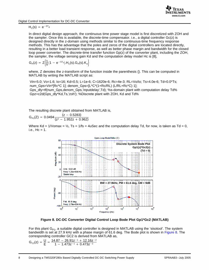
The resulting discrete plant obtained from MATLAB is,
Where Kd = 1/Vomax = ½, Ts = 1/fs = 4uSec and the computation delay Td, for now, is taken as Td = 0,i.e., Hc = 1.
Figure 8. DC-DC Converter Digital Control Loop Bode Plot Gp1*Gc2 (MATLAB)
For this plant GP1, a suitable digital controller is designed in MATLAB using the ‘sisotool’. The systembandwidth is set at 27.9 kHz with a phase margin of 61.6 deg. The Bode plot is shown in Figure 8. Thecorresponding controller GC2 is derived from MATLAB as,
Designing a TMS320F280x Based Digitally Controlled DC-DC Switching Power Supply8 SPRAAB3–July 2005

www.ti.com
U(n)� 1.473U(n� 1)� 0.4731U(n� 2)� 14.87E(n)� 26.91E(n� 1)� 12.16E(n� 2)
GP2(z)�(0.022z2� 0.017z� 0.0158)
z(z2� 1.952z� 0.962)
�HC � �Td � (360f)(0.5Ts) � 20 deg
Gp2(z)*Gc2(z)
Digital Control Implementation for DC-DC Converter
In discrete form, this controller is written as,
This controller was implemented using the TMS320F280x DSP instruction set. The corresponding codelisting is given in the zip file associated with this application report. The fixed point format used for thesecontroller coefficients is Q26.
Case 1 : Computation Delay Td = 0.5Ts
For the controller just designed we assumed Td = 0, which is not the case if we implement this controllerusing the sampling scheme shown in Figure 2. So, we recalculate Gp(z) for T= 0.5Ts to include the effectof the sampling scheme shown in Figure 2. Thus, by setting Td=0.5Ts in the MATLAB script shownbefore, the modified plant model is obtained as,
The corresponding Bode plot for this plant Gp2(z) with the controller Gc2(z) is shown in Figure 9. Fromthe two plots of Gp1*Gc2 and Gp2*Gc2, it is clear that the same controller Gc2 results in a phase marginreduction by 20.6 deg (= 61.6-41.0) for the latter system. This reduction in phase margin can beaccounted for by the computation time delay of Td = 0.5Ts associated with Gp2. This time delay translatesto a phase lag of,
where, Ts = 4uS, and f ≈ 27kHz is the cross-over frequency at which the phase lag is calculated.
Figure 9. DC-DC Converter Digital Control Loop Bode Plot Gp2*Gc2 (MATLAB)
SPRAAB3–July 2005 Designing a TMS320F280x Based Digitally Controlled DC-DC Switching Power Supply 9

www.ti.com
Digital Control Implementation for DC-DC Converter
The actual system Bode plot for the digitally controlled dc-dc converter represented by the plant modelGp2(z) and controlled by the controller Gc2(z) is shown in Figure 10. Notice that the frequency domainperformance parameters (bandwidth, phase margin and gain margin) agree quite well between the actualand the designed values. The time domain dynamic performance of the converter is shown in Figure 11.For a step load change of 15A, the output voltage settles within 28uSec (1% band). These test results onthe frequency and time domain characteristics of the digitally controlled converter show the validity of theMATLAB based design approach as illustrated by Figure 8 and Figure 9 above.
Figure 10. DC-DC Converter Control Loop Bode Plot Gp2*Gc2 (Test result from prototype h/w)
Designing a TMS320F280x Based Digitally Controlled DC-DC Switching Power Supply10 SPRAAB3–July 2005

www.ti.com
GP3(z)�(0.022z2� 0.017z� 0.0159)
z2(z2� 1.954z� 0.963)
Digital Control Implementation for DC-DC Converter
Figure 11. DC-DC Converter Load Transient Response (Loop gain = Gp2*Gc2)
Case 2 : Computation Delay Td = 2.0Ts
The sampling scheme shown Figure 2 can be modified to investigate the effect of a more severecomputation delay of Td = 2.0Ts. This is easily done in software by changing the interrupt scheme and theway the actual PWM duty ratio is updated following a new AD conversion of the output voltage. Once thisis done in software, the new plant model Gp3, for Td = 2Ts, is computed using MATLAB as,
The corresponding Bode plot for this plant Gp3(z) with the controller Gc2(z) is shown in Figure 12.
SPRAAB3–July 2005 Designing a TMS320F280x Based Digitally Controlled DC-DC Switching Power Supply 11

www.ti.com
�HC � �Td � (360 f)(2.0Ts) � 80 deg
GC3(z)� UE�
14.4� 31.1z�1� 20.1z�2� 3.376z�3
1� 1.235z�1� 0.2362z�2� 0.00115z�3
� U(n) � 1.235U(n � 1) � 0.2362U(n � 2) � 0.00115U(n � 3)
� 14.4E(n) � 31.1E(n � 1) � 20.1E(n � 2) � 3.376E(n � 3)
Digital Control Implementation for DC-DC Converter
Figure 12. DC-DC Converter Digital Control Loop Bode Plot Gp3*Gc2 (MATLAB)
From the plot of Figure 12 it is clear that this system is completely unstable when controlled by thecontroller Gc2. Comparing the plots of Gp1*Gc2 and Gp3*Gc2 we note that the controller Gc2 results in aphase margin reduction by 80.6 deg [= 61.6-(-19.0)] for the latter system. This reduction in phase marginis again accounted for by the computation time delay of Td = 2.0Ts associated with Gp3. This time delaytranslates to a phase lag of,
where, Ts = 4uS, and f ≈ 27kHz is the loop cross-over frequency at which the phase lag is calculated. Inorder to find a stable controller for Gp3, we note that this plant has 4-poles and 2 zeros and, therefore, the2-pole 2-zero controller Gc2 cannot stabilize the system. So, using MATLAB a new 3-pole 3-zerocontroller Gc3 is designed as,
The corresponding Bode plot for this plant Gp3(z) with the new controller Gc3(z) is shown in Figure 13.
The actual system Bode plot for the dc-dc converter represented by this plant model Gp3(z) and controlledby the redesigned controller Gc3(z) is shown in Figure 14. It is again clear that the frequency domaincharacteristics match very closely between the actual and the designed values.
Designing a TMS320F280x Based Digitally Controlled DC-DC Switching Power Supply12 SPRAAB3–July 2005

www.ti.com
Gp3(z)*Gc3(z)
BW = 15.28kHz, PM = 41.76 deg, GM = 3.4dB
Digital Control Implementation for DC-DC Converter
Figure 13. DC-DC Converter Digital Control Loop Bode Plot Gp3*Gc3 (MATLAB)
Figure 14. DC-DC Converter Load Transient Response (Loop gain = Gp3*Gc3)
SPRAAB3–July 2005 Designing a TMS320F280x Based Digitally Controlled DC-DC Switching Power Supply 13

www.ti.com
3 Conclusion
Conclusion
Figure 15 shows the converter output voltage transient response with this controller. For a step loadchange of 15A, the output voltage settles within 50uSec (1% band). These test results again show thevalidity of the MATLAB based design approach as depicted in Figure 12 and Figure 13 above.
Figure 15. DC-DC Converter Load Transient Response (Loop gain = Gp3*Gc3)
DSP based digital control design methods for high frequency dc-dc buck converter is investigated usingMATLAB based control design tools. Starting with a buck converter interfaced to a DSP controller,different control blocks and associated parameters are identified prior to the digital controller design. Twoapproaches to the digital controller design are presented. The first method, namely design by emulation,allows the power supply designers to do the control design in the familiar s-domain and then convert it to adiscrete/digital controller. The second approach known as direct digital design, illustrates digital controllerdesign directly in z-domain. It was found that the later approach results in a better dynamic performancefor the closed loop operation of the converter. All of these MATLAB based designed controllers werefinally validated by experimental results.
Designing a TMS320F280x Based Digitally Controlled DC-DC Switching Power Supply14 SPRAAB3–July 2005

www.ti.com
4 References
References
1. S. Bibian, H. Jin, “Digital control with improved performance for boost power factor correction circuits”APEC, March 2001 pp:137 - 143
2. Jinghai Zhou, etc., “Novel sampling algorithm for DSP controlled 2 kW PFC converter”, PowerElectronics, IEEE Transactions, March 2001, pp: 217 – 222
3. P. Zumel, etc., “Concurrent and simple digital controller of an AC/DC converter with power factorcorrection”, APEC 2002, pp: 469 – 475
4. Wanfeng Zhang, etc., “DSP implementation of predictive control strategy for power factor correction”,APEC, Feb. 2004, pp: 67 - 73
5. Y. Duan, H. Jin, “Digital controller design for switch mode power converters”, APEC ’99, Volume: 2, pp:967 – 973.
6. Average Current Mode Controlled Power Factor Correction Converter using TMS320LF2407(SPRA902A)
7. Prodic, A.; Maksimovic, D.; Erickson, R.W., “Design and implementation of a digital PWM controller fora high-frequency switching DC-DC power converter”, Industrial Electronics Society, 2001. IECON2001, Volume: 2, 29 Nov.-2 Dec. 2001, pp: 893 - 898
8. S. Choudhury, “DSP Implementation of an average current mode controlled Power Factor CorrectionConverter”, International Power Elect Technology Conference Proceeding, Nov 4-6, 2003.
9. G. F. Franklin & J. D. Powell, ”Digital Control of Dynamic Systems”, Addision-Wesley PublishingCompany, 1998, pp: 189-204.
SPRAAB3–July 2005 Designing a TMS320F280x Based Digitally Controlled DC-DC Switching Power Supply 15

IMPORTANT NOTICE
Texas Instruments Incorporated and its subsidiaries (TI) reserve the right to make corrections, modifications,enhancements, improvements, and other changes to its products and services at any time and to discontinueany product or service without notice. Customers should obtain the latest relevant information before placingorders and should verify that such information is current and complete. All products are sold subject to TI’s termsand conditions of sale supplied at the time of order acknowledgment.
TI warrants performance of its hardware products to the specifications applicable at the time of sale inaccordance with TI’s standard warranty. Testing and other quality control techniques are used to the extent TIdeems necessary to support this warranty. Except where mandated by government requirements, testing of allparameters of each product is not necessarily performed.
TI assumes no liability for applications assistance or customer product design. Customers are responsible fortheir products and applications using TI components. To minimize the risks associated with customer productsand applications, customers should provide adequate design and operating safeguards.
TI does not warrant or represent that any license, either express or implied, is granted under any TI patent right,copyright, mask work right, or other TI intellectual property right relating to any combination, machine, or processin which TI products or services are used. Information published by TI regarding third-party products or servicesdoes not constitute a license from TI to use such products or services or a warranty or endorsement thereof.Use of such information may require a license from a third party under the patents or other intellectual propertyof the third party, or a license from TI under the patents or other intellectual property of TI.
Reproduction of information in TI data books or data sheets is permissible only if reproduction is withoutalteration and is accompanied by all associated warranties, conditions, limitations, and notices. Reproductionof this information with alteration is an unfair and deceptive business practice. TI is not responsible or liable forsuch altered documentation.
Resale of TI products or services with statements different from or beyond the parameters stated by TI for thatproduct or service voids all express and any implied warranties for the associated TI product or service andis an unfair and deceptive business practice. TI is not responsible or liable for any such statements.
Following are URLs where you can obtain information on other Texas Instruments products and applicationsolutions:
Products Applications
Amplifiers amplifier.ti.com Audio www.ti.com/audio
Data Converters dataconverter.ti.com Automotive www.ti.com/automotive
DSP dsp.ti.com Broadband www.ti.com/broadband
Interface interface.ti.com Digital Control www.ti.com/digitalcontrol
Logic logic.ti.com Military www.ti.com/military
Power Mgmt power.ti.com Optical Networking www.ti.com/opticalnetwork
Microcontrollers microcontroller.ti.com Security www.ti.com/security
Telephony www.ti.com/telephony
Video & Imaging www.ti.com/video
Wireless www.ti.com/wireless
Mailing Address: Texas Instruments
Post Office Box 655303 Dallas, Texas 75265
Copyright 2005, Texas Instruments Incorporated