Embed Size (px)
Citation preview

12ICLAB NCTU Institute of Electronics
Design Scope of Verilog
We use Verilog HDL to design– Typical design flow
Verilog HDL
Design Specification
Algorithmic Model
RTL Model
Gate-Level Model
Physical Layout
Switch-Level Model
Structurallanguage
Behavior language
RAM ALU
PLA
ROM
IO
13ICLAB NCTU Institute of Electronics
What is Verilog?
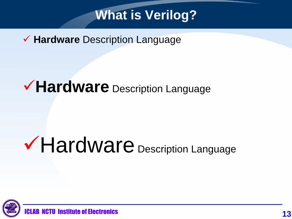
Hardware Description Language
Hardware Description Language
Hardware Description Language

17ICLAB NCTU Institute of Electronics
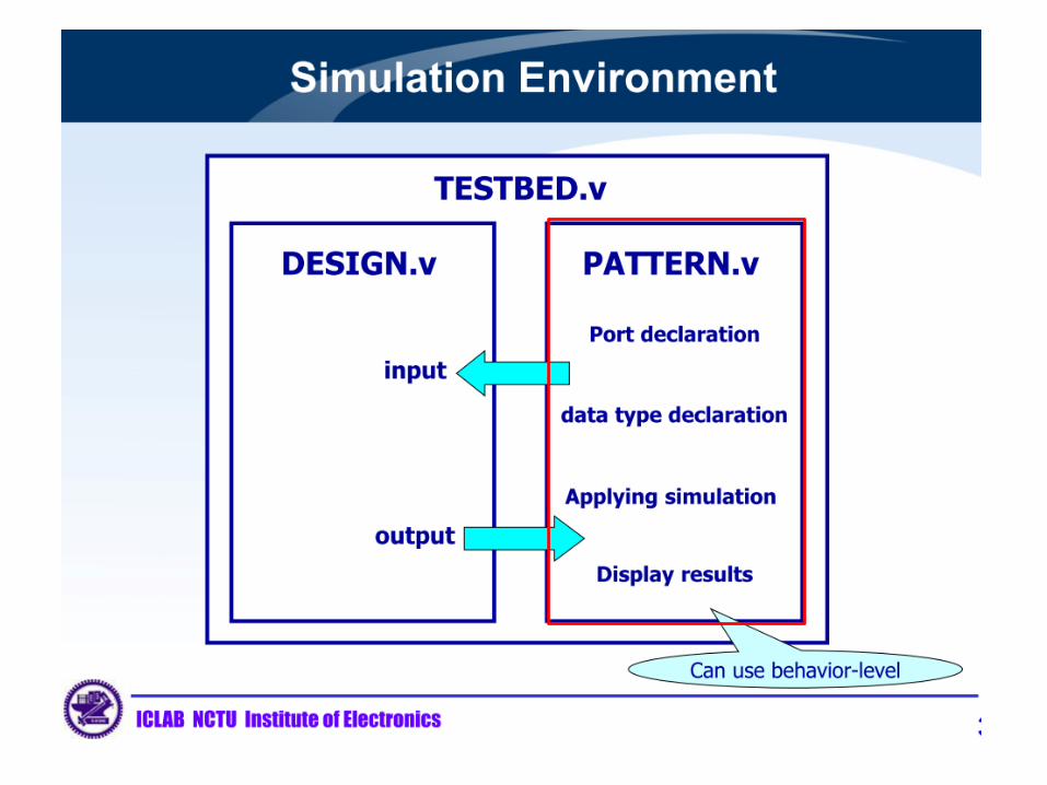
Lexical Convention : A Module
module module_name(port_list);
endmodule
port declaration
data type declaration
task & function declaration
module functionality or structure
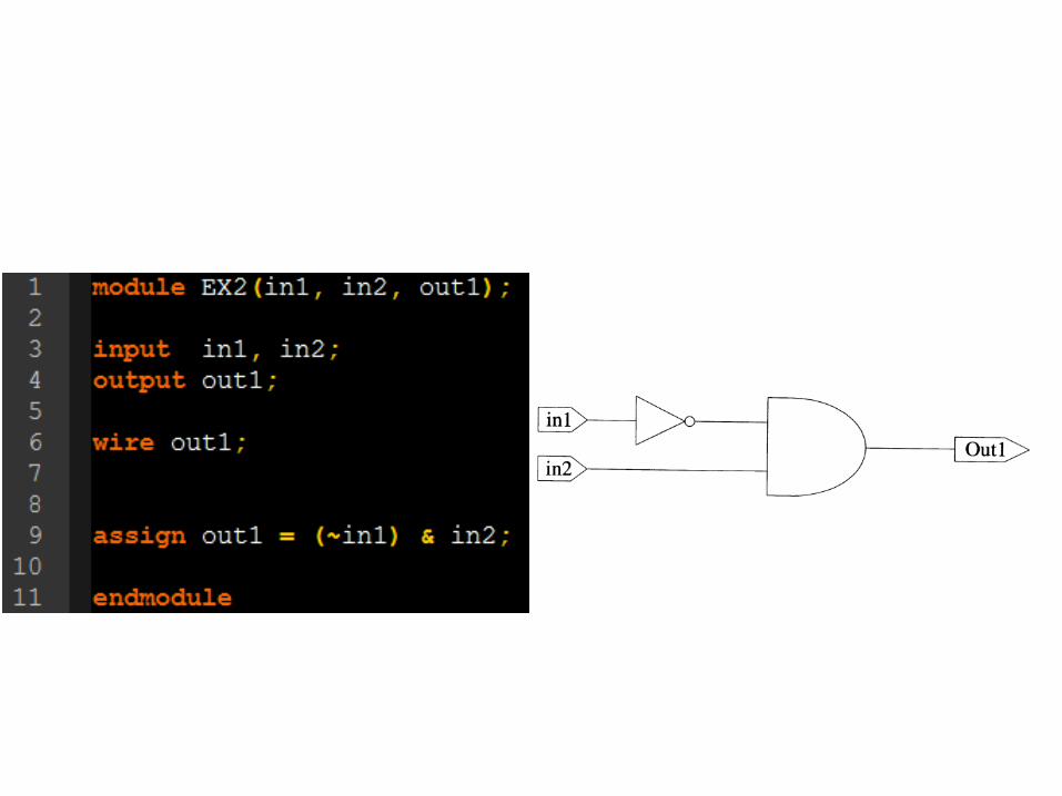
module test ( Q,S,clk );
output Q;
input S,clk;
reg Q;
always@(S or clk)
Q<=(S&clk) ;
endmodule
Encapsulate structural and functional details
All modules run concurrently
Encapsulation makes the model available for instantiation in other
modules

18ICLAB NCTU Institute of Electronics
Lexical Convention : Identifier and Comment
Verilog is a case sensitive language
Terminate lines with semicolon ;
Identifiers– starts only with a letter or an _(underscore), can be any
sequence of letters, digits, $, _ .– case-sensitive !
• e.g. shiftreg_a
_bus3
n$657
12_reg illegal !!!!
Comments– single line : //– multiple line : /* … */

20ICLAB NCTU Institute of Electronics
Lexical Convention : Number
Number Specification
– <size>’<base><value>
• <size> is the length of desired value in bits.
• <base> can be b(binary), o(octal), d(decimal) or h(hexadecimal).
• <value> is any legal number in the selected base.
[When <size> is smaller than <value>: left-most bits of <value>are truncated
When <size> is larger than <value>, then left-most bits are filled based on the value of the left-most bit in <value>.]
Left most '0' or '1' are filled with '0', 'Z' are filled with 'Z' and 'X‘ with 'X'
• Default size is 32-bits decimal number
• e.g. 4’d10 4-bit, 10, decimal
• e.g. 6’hca 6-bit, store as 6’b001010 (truncated, not 11001010!)
• e.g. 6’ha 6-bit, store as 6’b001010 (filled with 2-bit ‘0’ on left!)
• Extension:
• 12’hz zzzz zzzz zzzz;6’bx xx xxxx;8’b0 0000 0000;8’b1 0000 0001
– Negative : -<size>’<base><value>
• e.g. –8’d3 legal 8’d–3 illegal

21ICLAB NCTU Institute of Electronics
Lexical Convention : Operator
Operators– Arithmetic Description
• A = B + C;
• A = B – C;
• A = B * C;
• A = B / C;
• A = B % C; modulus some synthesis tools don’t support this operator
– Shift Operator (bit-wise)• A = B >> 2; shift right ‘B’ by 2-bit
• A = B << 2; shift left ‘B’ by 2-bit
– Shift Operator (arithmetic)• A = B >>> 2;
• A = B <<< 2;
• e.g. B = 4’b1000;
A = B >>>2;
“>>>”, ”<<<“ are used only for ‘signed’ data type in Verilog 2001
(A = 4’b1110 ,which is 1000 shifted to the right two positions and sign-filled.)

22ICLAB NCTU Institute of Electronics
Lexical Convention : Operator
Bit-wise Operator– NOT: A = ~ B;
– AND: A = B & C;
– OR: A = B | C;
– XOR: A = B ^ C;
– e.g. 4’b1001 | 4’b1100 4’b1101
Logical Operators: return 1-
bit true/false– NOT: A = ! B;
– AND: A = B && C;
– OR: A = B || C;
– e.g. 4’b1001 || 4’b1100 true,
1’b1
Conditional Description– if else
– case endcase
– ? : c = sel ? a : b;// if (sel==1’b1)
// c = a;
// else
// c = b;
Relational and
equality(conditional)– <=, <, >, >=, ==, !=
– i.e. if( (a<=b) && (c==d) || (e>f))

24ICLAB NCTU Institute of Electronics
Lexical Convention : Concatenation
– Concatenation
• { } a = {b, c};
• {{}} a = {2{c}};
• a[4:0] = {b[3:0],1’b0}; a = b << 1;
b[3]
b[0]
c[3]
c[0]
a[7]
a[0]
……
……
…
C[3]
C[0]
a[7]
a[0]
……

25ICLAB NCTU Institute of Electronics
Data Type
4-value logic system in Verilog: 0, 1, x or X, z or Z
Declaration Syntax<data_type>[<MSB> : <LSB>]<list_of_identifier>
– Nets : represent physical connections between devices (default=z)
• represent connections between things
• Cannot be assigned in an initial or always block
– Register : represent abstract data storage element (default=x)
• represent data storage
• Hold their value until explicitly assigned in an initial or always block
• Can be used to model latches, flip-flops, etc., but do not correspond exactly
Register type Attribute
reg Unsigned value with Varying bit width
integer 32-bit signed (2’s complement)
time 64-bit unsigned
real Real number

26ICLAB NCTU Institute of Electronics
Data Type : Vector and Array
– Vectors : the wire and register can be represented as a vector
• wire [7:0] vec; 8-bit bus
• reg [0:7] vec; vec[0] is the MSB
– Arrays : <array_name>[<subscript>]
It isn’t well for the backend verifications
• integer mem[0:7] (8x32)-bit mem
• reg [7:0] mem[0:1023] Memories!! (1k - 1byte)
– What’s difference between Vector and Array?
• Vector : single-element with multiple-bit
• Array : multiple-element with multiple-bit
:
:
Memory(Array)
Vector
For this reason, we do not use array as memory, Memory component will be introduced later

29ICLAB NCTU Institute of Electronics
Port : Module Connection
Port ordering– one port per line with appropriate comments
– inputs first then outputs
– clocks, resets, enables, other controls, address bus, then data bus
Modules connected by port order (implicit)– Here order shall match correctly. Normally, it not a good idea to
connect ports implicitly. It could cause problem in debugging when any new port is added or deleted.
– e.g. : FA U01( A, B, CIN, SUM, COUT );
Modules connect by name (explicit)– Use named mapping instead of positional mapping
– name shall match correctly.
– e.g. : FA U01( .a(A), .b(B), .cin(CIN), .sum(SUM), .cout(COUT) ); foo u_foo1(4’h2, 4’h5, 4’h8); X
Use this!!!

36ICLAB NCTU Institute of Electronics
Data Assignment
Continuous Assignment for wire assignment– Imply that whenever any change on the RHS of the assignment occurs, it
is evaluated and assigned to the LHS.
• e.g. wire [3:0] a;assign a = b + c; //continuous assignment
Procedural Assignment for reg assignment– assignment to “register” data types may occur within always,
initial, task and function. These expressions are controlled by triggers which cause the assignment to evaluate.
• e.g. reg a,clk;always #5 clk = ~clk; //procedural assignment
• e.g. always @ (b) //procedural assignment with triggers
a = ~b;
38ICLAB NCTU Institute of Electronics
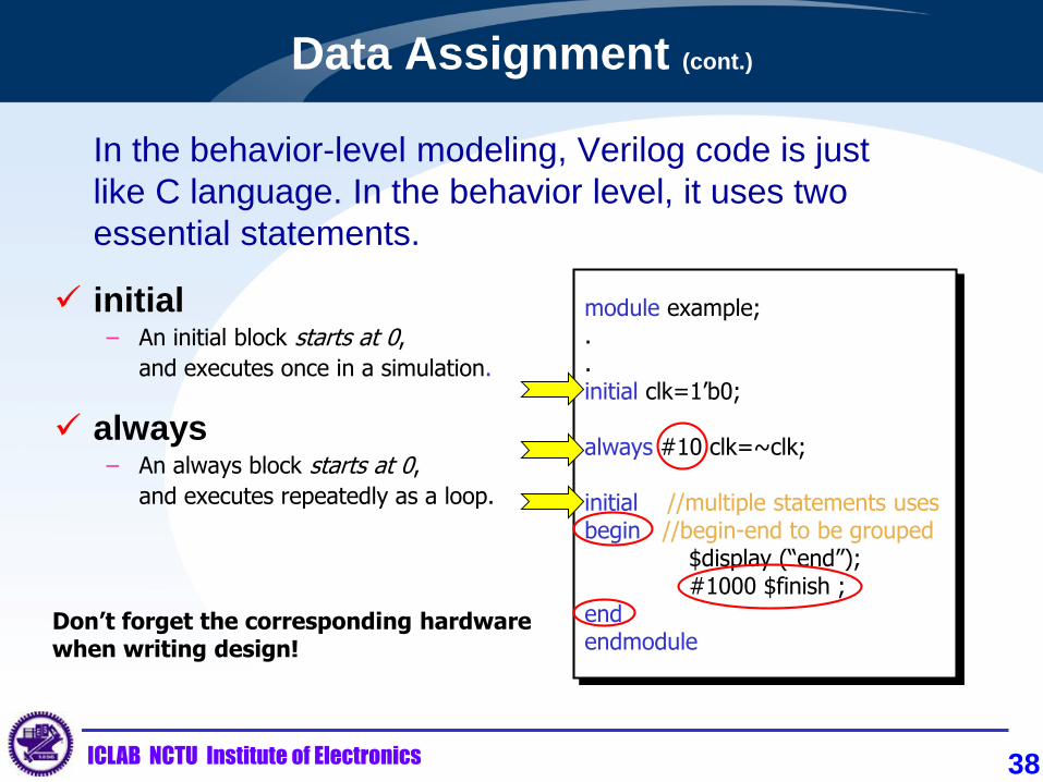
Data Assignment (cont.)
In the behavior-level modeling, Verilog code is just
like C language. In the behavior level, it uses two
essential statements.
initial– An initial block starts at 0,
and executes once in a simulation.
always– An always block starts at 0,
and executes repeatedly as a loop.
module example;..initial clk=1’b0;
always #10 clk=~clk;
initial //multiple statements usesbegin //begin-end to be grouped
$display (“end”);#1000 $finish ;
endendmodule
Don’t forget the corresponding hardware when writing design!


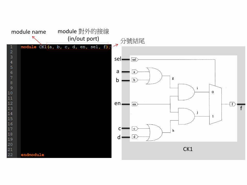
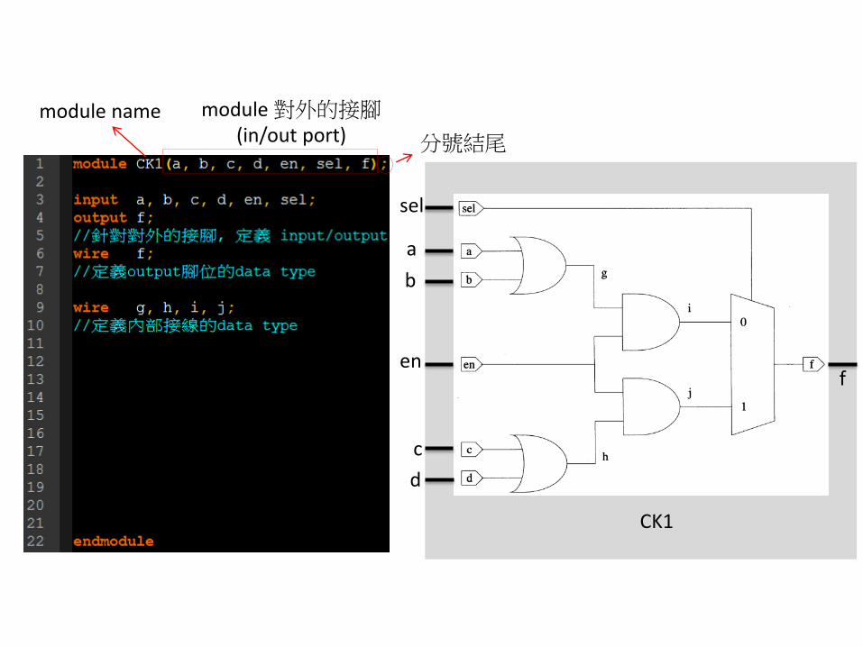
CK1
f
sel
a
b
en
c
d
CK1
f
sel
a
b
en
c
d
module name module對外的接線(in/out port) 分號結尾

CK1
f
sel
a
b
en
c
d
module name module對外的接腳(in/out port) 分號結尾

CK1
f
sel
a
b
en
c
d
module name module對外的接腳(in/out port) 分號結尾
CK1
f
sel
a
b
en
c
d
module name module對外的接腳(in/out port) 分號結尾

CK1
f
sel
a
b
en
c
d
module name module對外的接腳(in/out port) 分號結尾


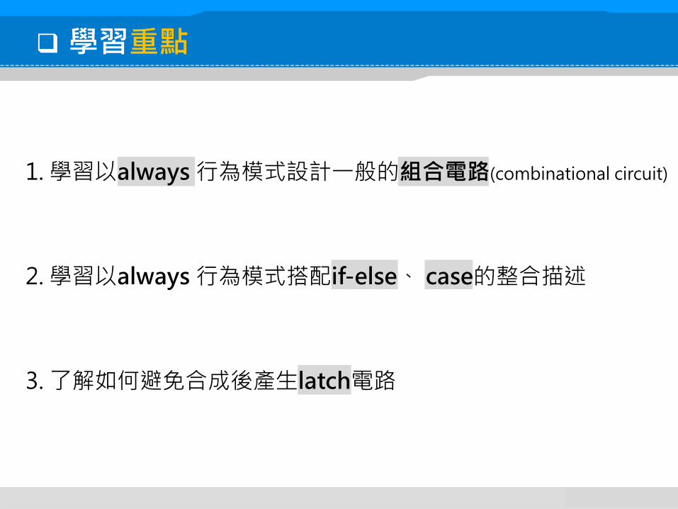
學習重點
1. 學習以always 行為模式設計一般的組合電路(combinational circuit)
2. 學習以always 行為模式搭配if-else、 case的整合描述
3. 了解如何避免合成後產生latch電路

以always behavior model 設計電路
data flow 的方式描述電路 behavior module 描述電路

always behavior model

以always behavior model 設計電路

以always + if-else 設計多工器

以always + case 設計多工器
select line
sel的可能值 對應的運算
defaul代表sel的其他情況都會落入deault值 執行對應的運算
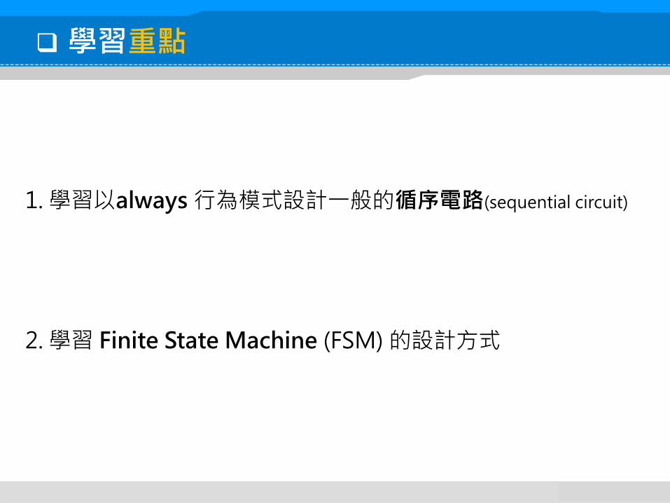
學習重點
1. 學習以always 行為模式設計一般的循序電路(sequential circuit)
2. 學習 Finite State Machine (FSM) 的設計方式
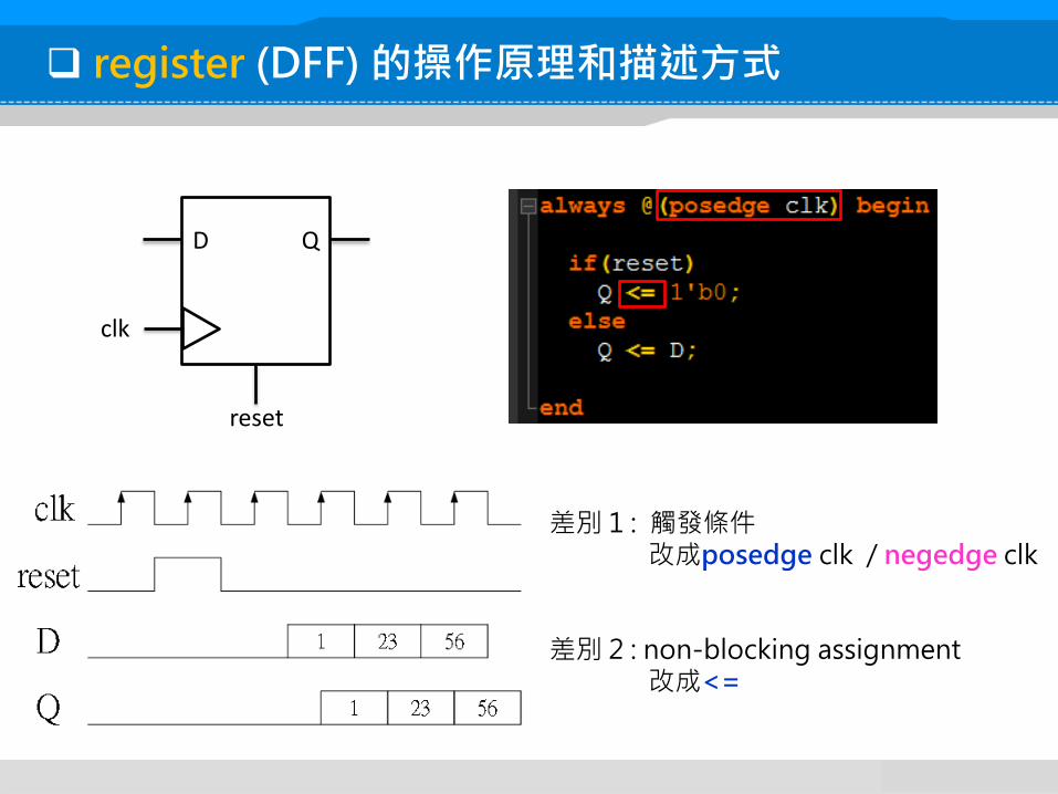
register (DFF) 的操作原理和描述方式
clk
reset
D Q
差別 1 : 觸發條件 改成posedge clk / negedge clk
差別 2 : non-blocking assignment 改成<=

設計sequential電路的技巧
clk
reset
out_w out Q D
00
01
10
11
a
b
c
d
sel
1. 命名技巧 : DFF前面 input data 的接線命名成_w
2. 將 register 和 combinational 分開寫


![Chapter 04 [相容模式]twins.ee.nctu.edu.tw/courses/co_16/Chapter_04.pdf · Memory reference: lw, sw Arithmetic/logical operation: add, sub, and, or, slt Program flow control: beq,](https://img.dokumen.tips/doc/110x75/605ab3d0e6912e494b4eba88/chapter-04-ctwinseenctuedutwcoursesco16chapter04pdf-memory.jpg)


![Chapter 04 [相容模式] - twins.ee.nctu.edu.twtwins.ee.nctu.edu.tw/courses/co_15/Chapter_04.pdf · How the choice of various implementation strategies affects the ... (sequential)](https://img.dokumen.tips/doc/110x75/5ab7f60f7f8b9ac10d8c63a6/chapter-04-twinseenctuedu-the-choice-of-various-implementation.jpg)

![Chapter 06 [相容模式] - twins.ee.nctu.edu.twtwins.ee.nctu.edu.tw/courses/co_16/Chapter_06.pdf · Introduction Goal: connecting multiple computers to get higher performance Multiprocessors](https://img.dokumen.tips/doc/110x75/5e6c293cf0020b16e94df5c4/chapter-06-c-twinseenctuedu-introduction-goal-connecting-multiple.jpg)