Embed Size (px)
Citation preview

32nm 1-D Regular Pitch SRAM Bitcell Design for
Interference-Assisted Lithography
Bob Greenway: Petersen Advanced LithographyKwangok Jeong: ECE Department, UCSDAndrew B. Kahng: ECE/CSE Department, UCSDChul-Hong Park: ECE Department, UCSDJohn S. Petersen: Petersen Advanced Lithography
UCSD VLSI CAD Laboratory
*
*
1 of 22

Outline
Interference-Assisted Lithography (IAL) IAL Friendly SRAM Bitcell Design
IAL Friendly Layout: Grid-Based Layout Summary of SRAM Bitcell Design Proposed Bitcell Layout
Simulation Results Lithography Simulation Electrical Characteristics
Conclusion and Ongoing Work
UCSD VLSI CAD Laboratory 2 of 22

Interference-Assisted Lithography
Low cost litho.(Mask, RET, etc.)
Maskless
Dense / high contrast /high resolution grating patterns
Interference Lithography (IL)
ProjectionLithography (PL)
resistphotoacid distribution
Trim aerial image
Trim mask resolution>> IL resolution
Lower cost than EUV and IArFHigher throughput than E-beam
Least Line-End RoughnessUCSD VLSI CAD Laboratory 3 of 22

IAL-Friendly Layout Limitation of IAL
IL can print only 1-D grating patterns. What does IAL-friendly layout look like?
Patterns must be on grid Patterns must have only 1-D geometries
Problems De-compacting onto a grid increases area Difficult to make 1-D patterns without using more layers.
Contact pitch Poly pitch
(Figure courtesy J. Wang et al., J. Microlith., 2005)
UCSD VLSI CAD Laboratory 4 of 22

IAL to SRAM Design
We focus on 1-D regular pitch layout for SRAM bitcell SRAM blocks can occupy > 50% of die in today’s SOC
Improveing the bitcell Strong area impact Regular structure: examples of 6-T bitcell layouts in 65nm
Easy to transform
TI 65nm: 0.46x1.06um2
IBM 65nm: 0.41x1.25um2
Intel 65nm: 0.46x1.24um2
* Figures courtesy A. Chatterjee et al., P. Bai et al., and Z. Luo et al., Int. Electron Device Meeting Tech. Digest, 2004
UCSD VLSI CAD Laboratory 5 of 22

NL NL NR NRWLWL
VDD
VDDVSS
VSSBLB
BL
SRAM Bitcell Design
PG1
PU1
PD1PG2
PU2
PD2
VDD
VSSBLB BL
WL
NL NR
UCSD VLSI CAD Laboratory 6 of 22
PG1
PG2
PD2
PD1
PU2
PU1
Schematic Layout Micrograph
Requirements of SRAM bitcell design Stable read operation: Do not disturb written data when reading Stable write operation: Must write a correct data within a specified time Stable data retention: Data should not be lost
Rules of thumb for transistor sizing Cell ratio (= I(PD) / I(PG)) = 1.5 ~ 2.5 Pull-up ratio (= I(PU) / I(PG)) = 0.5
PG1
PU1
PD1PG2
PU2
PD2
IAL Friendly SRAM Bitcell Layout Fixed POLY (H), CNT (V), M1 (H), V1 (V),
…, directions Vertical: 2 poly pitch Horizontal: 5 contact pitch
Poly-to-contact space > overlay + spacer + strain_layer + CD_control (6.4nm*) ( 8nm**) (10nm**) ( 2.6nm*) = 27nm
1 poly pitch = 2 poly_to_contact + poly_width + contact_width 54 + 32 + 45** = 131 nm
A pitch is a multiple of a drawing grid for fine-grain pattern placement Ex.: 5 grid per pitch drawing grid = (131/5) = 26 nm Ex.: 6 grid per pitch drawing grid = (131/6) = 22 nm
UCSD VLSI CAD Laboratory 7 of 22
polyspacer
Strain layer
CNT * From ITRS 32nm tech.** From S. Verhaegen et al., SPIE Adv. Litho., 2008

Design Rule Context
Design Rule Item 5-grid rule 6-grid rule ITRS(32nm)Unit drawing grid size 26 nm (=1 grid) 22 nm (=1 grid) -
Mx: min. width/space 52 nm (=2 grid) 44 nm (=2 grid) ~32 nm
Contact/Via: width/space 52 nm (=2 grid) 44 nm (=2 grid) 39 nm (resist)
Diffusion: min. width/space 52 nm (=2 grid) 44 nm (=2 grid) -
Poly-to-contact space 23 nm 28 nm -
Poly pitch 130 nm 132 nm
Based on the drawing grid size, minimum required design rules are defined
Bit cell size 25x10 w/ 5-grid rule 30x12 w/ 6-grid rule 25x12 grids w/ 6-grid ruleX-dimension 650 nm 660 nm 550 nm
Y-dimension 260 nm 264 nm 264 nm
Area 0.169 um2 0.174 um2 0.145 um2
Three example bitcells
UCSD VLSI CAD Laboratory 8 of 22

Alternative Bitcell Layouts
(a) 25x10: 5-grid rule (b) 30x12: 6-grid rule (c) 25x12: 6 grid rule
POLY and DIFF
CNT
M1
UCSD VLSI CAD Laboratory 9 of 22

Layout for 25x12 bitcell: NWELL to METAL1
WL
VSS
BLB
nl nl
VDD
VDD
nr nr WL
VSS
BL
NWELL
DIFF
POLY
CNT
METAL1
UCSD VLSI CAD Laboratory 10 of 22
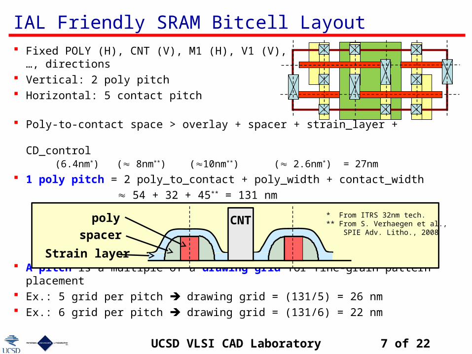
Layout for 25x12 bitcell: METAL2 to METAL4
METAL1
WL
VSS
BLB
nl nl
VDD
VDD
nr nr WL
VSS
BL
METAL2
VIA1
VIA2
METAL3
VIA3
METAL4
UCSD VLSI CAD Laboratory 11 of 22

Lithography Simulation Conditions
Simulator: Dr. Litho version 0.10.5 (Fraunhofer IISB)
Full vector models thin mask for initial work
High contrast positive resist (50nm) model parameters
Simulation with only a simple OPC correction using biasing
Illuminator (XQUAD) setting for block exposure
with NA =1.2 of 66nm/90nm IL pitch
We develop solutions for all layers except diffusion layer
UCSD VLSI CAD Laboratory 12 of 22

Poly: 66nm IL + 66nm Binary Blocking Mask
Blocking Mask (Black = clear)
UCSD VLSI CAD Laboratory 13 of 22
Blue=Resist
Positive Resist

Contact: 90nm CPA Mask Xquad 0.94/0.1
Black=Clear & White=Quartz etch
Blocking Mask
Green=Resist
Negative Resist
UCSD VLSI CAD Laboratory 14 of 22

Metal1: 90nm IL + CPA w/Chrome Assist Xquad 0.94/0.1
Blocking Mask
Green=Resist
Black=Clear & White=Quartz etchNarrow, Long and Black=Chrome assists
Negative Resist
UCSD VLSI CAD Laboratory 15 of 22

VIA1: 90nm IL + CPA MASK
Black=Clear & White=Quartz etch
Blocking Mask
Image 1 formed with 4-beam interference
Green=Resist
UCSD VLSI CAD Laboratory 16 of 22
We can make very high density hole arrays, if we can do four-beam interference exposure

Electrical Characteristics: Experimental Setup
In this study, we compare Butterfly (read stability) N-curves (read and write stability) Iread (read stability and access time) VDDHOLD (data retention) Ileakage (power and data retention)
SPICE Model: 32nm HKMG (high-K/metal-gate)
from PTM Reference Design
Scaled bitcell from TSMC 90nm bitcell
UCSD VLSI CAD Laboratory 17 of 22
TSMC 90nm 32nm scaled from TSMC
90nm(REFERENCE)
32nm proposed(for 30x12, 25x12)
L (nm) W (nm) L (nm) W (nm) L (nm) W (nm)
Pull-up 100 100 32 32 32 44
Pull-down 100 175 32 56 32 88
Pass-Gate 115 120 37 38 32 44

Butterfly and N-Curves Measure method
Increase VR and measure VL Increase VL and measure VR Make voltage transfer curve in VR
and VL axes Butterfly Measure Iin N-curve
0.0
0.1
0.2
0.3
0.4
0.5
0.6
0.7
0.8
0.9
1.0
0 0.2 0.4 0.6 0.8 1
Scaled layout from TSMC90(All dimensions are scaled by 0.32)
1-D regular pitch layout
-1.0E-04
0.0E+00
0.00
0.07
0.14
0.21
0.28
0.35
0.42
0.49
0.56
0.63
0.70
0.77
0.84
0.91
0.98
32nm (Scaled from TSMC90)32nm 1-D regular
WTV
SVNM
SINM_reg
SINM_TSMC
SINM_TSMCSINM_reg
UCSD VLSI CAD Laboratory 18 of 22

Iread, Ileakage and VDDHOLD
REFERENCE 32nm proposed(for 30x12 and 25x12)
Iread 41.2 uA 66.7 uA
Ileakage 85.4 nA 142.7 nA
VDDHOLD 110 mV 118 mV
Iread
Measure bitline current when WL switches to high
ILEAKAGE
Measure VDD (or VSS) current when WL=0
VDDHOLD
Decreasing VDD voltage, while WL=0 Measure minimum VDD voltage when
| V(nl) - V(nr) | = ‘sensing margin’
A1 A2
B1 B2
C1 C2 nl nr
VDD
WL
BLb BL
‘0’‘1’
‘1’ ‘1’
(100mV is assumed)
UCSD VLSI CAD Laboratory 19 of 22
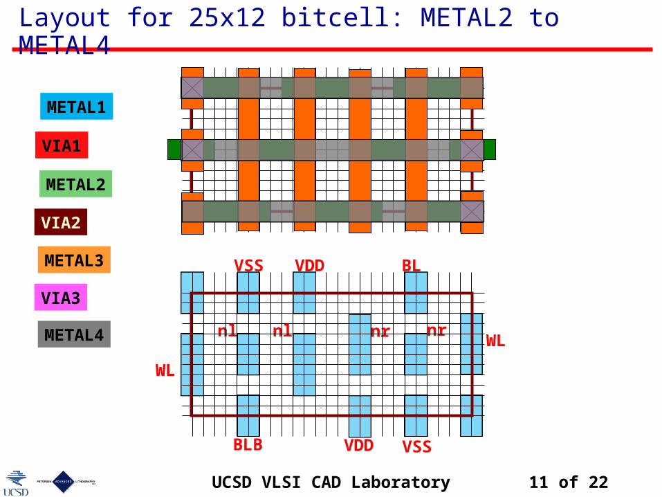
Corner Simulation: Butterfly and N-Curve
Three candidate layouts across operating corners show little difference
(NN, 25degC, 1.0V)(SS, 125degC, 1.0V) (FF, -40degC, 1.0V)
0.00E+00
2.00E-01
4.00E-01
6.00E-01
8.00E-01
1.00E+00
1.20E+00
0 0.2 0.4 0.6 0.8 1 1.2
25x10, FF, -40degC25x12, FF, -40degC30x12, FF, -40degC
0.00E+00
2.00E-01
4.00E-01
6.00E-01
8.00E-01
1.00E+00
1.20E+00
0 0.2 0.4 0.6 0.8 1 1.2
25x10, NN, 25degC25x12, NN, 25degC30x12, NN, 25degC
0.00E+00
2.00E-01
4.00E-01
6.00E-01
8.00E-01
1.00E+00
1.20E+00
0 0.2 0.4 0.6 0.8 1 1.2
25x10, SS, 125degC25x12, SS, 125degC30x12, SS, 125degC
-1.5E-04
-1.0E-04
-5.0E-05
0.0E+00
5.0E-05
1.0E-04
1 611 16 21 26 31 36 41 46 51 56 61 66 71 76 81 86 91 96 10
1
25x1025x1230x12
-1.5E-04
-1.0E-04
-5.0E-05
0.0E+00
5.0E-05
1.0E-041 6
11 16 21 26 31 36 41 46 51 56 61 66 71 76 81 86 91 96 101
25x1025x1230x12
-1.0E-04
-5.0E-05
0.0E+00
5.0E-05
1.0E-04
1 611 16 21 26 31 36 41 46 51 56 61 66 71 76 81 86 91 96 101
25x1025x1230x12
UCSD VLSI CAD Labratory 20 of 22

Corner Simulation: Iread , Ileakage and VDDHOLD
VDDHOLD (V)
0.1120.1140.1160.118
0.120.1220.1240.1260.128
0.13
25x10 25x12 30x12 25x10 25x12 30x12 25x10 25x12 30x12
FF, -40 NN, 25 SS, 125
1.00E-10
1.00E-09
1.00E-08
1.00E-07
1.00E-06
1.00E-05
1.00E-04
0.1 0.2 0.3 0.4 0.5 0.6 0.7 0.8 0.9 1 1.1 1.2 1.3 1.4 1.5
FF, -40 25x10FF, -40 25x12FF, -40 30x12NN, 25 25x10NN, 25 25x12NN, 25 30x12SS, 125 25x10SS, 125 25x12SS, 125 30x12
0.00E+00
2.00E-05
4.00E-05
6.00E-05
8.00E-05
1.00E-04
1.20E-04
1.40E-04
1.60E-04
1.80E-04
0.1 0.2 0.3 0.4 0.5 0.6 0.7 0.8 0.9 1 1.1 1.2 1.3 1.4 1.5
FF, -40 25x10FF, -40 25x12FF, -40 30x12NN, 25 25x10NN, 25 25x12NN, 25 30x12SS, 125 25x10SS, 125 25x12SS, 125 30x12
Iread (A) Ileakage (A)
VDD (V) VDD (V)
UCSD VLSI CAD Laboratory 21 of 22
Conclusion and Ongoing work Conclusion
We propose a 1-D regular pitch bitcell layout methodology applicable to interference-assisted lithography (IAL)
We obtain successful lithography results for 32nm bitcell through IAL Except for poly IAL requires a negative tone solution
We evaluate the electrical characteristics of the proposed bitcells using 32nm PTM device models
Ongoing Work Hope to report results of Oct. 2008 tapeout at SPIE 2009 Stronger electrical / circuit validation with statistical analysis and
dynamic circuit analysis Development of a full 1-D regular pitch bitcell including diffusion layer
Acknowledgments We warmly thank Rudi Hendel and Zhilong Rao of Applied Materials,
Kevin Liu (formerly of Applied Materials), and R. Scott Mackay of Petersen Advanced Lithography for many helpful interactions
UCSD VLSI CAD Laboratory 22 of 22

THANK YOU VERY MUCH !
UCSD VLSI CAD Laboratory

Backup
VLSICAD Lab., UCSD 24 of 24

Lithography at 32nm and Below Major requirements of lithography
High throughput Low cost
Possible solutions for 32nm and below Double patterning lithography (DPL)
Relatively low throughput: two exposures High cost: two masks
Immersion ArF (IArF) High throughput High cost: high index fluid, complex RET, high cost optics
Extreme Ultra-Violet (EUV) High throughput High cost: high output power source, high reflectivity resist
Electron projection Low throughput: long exposure time Low cost: maskless lithography
VLSICAD Lab., UCSD 25 of 24

1-D Regular-Pitch Layout
IAL (Interference-Assisted Lithography) All features must be placed in a regular pitch Pitch is constrained by the resolution of the single
exposure technique Minimum pitch of single exposure at 32nm node: ~128nm
A pitch is multiple of an unit grid 1 pitch / 5 unit grid unit grid = (128/5) = 26 nm 1 pitch / 6 unit grid unit grid = (128/6) = 22 nm
VLSICAD Lab., UCSD 26 of 24

Available Pitches in IAL
To trim patterns by projection lithography, routing pitch is limited by the capability of the projection lithography
khp kpitch l NA Pitch (nm) w/no Process Dependence
Pitch (nm) w/Process Adjust Illuminator
0.375 0.75 193 0.93 156 173 Qudrupole0.3 0.6 193 0.93 125 138 Annulus or Cross-Quad
0.27 0.54 193 0.93 112 125 Cross-Quad0.25 0.5 193 0.93 104 115 Ideal (Dipole)
0.375 0.75 193 1.20 121 134 Qudrupole0.3 0.6 193 1.20 97 107 Annulus or Cross-Quad
0.27 0.54 193 1.20 87 97 Cross-Quad0.25 0.5 193 1.20 80 89 Ideal (Dipole)
0.375 0.75 193 1.35 107 119 Qudrupole0.3 0.6 193 1.35 86 95 Annulus or Cross-Quad
0.27 0.54 193 1.35 77 86 Cross-Quad0.25 0.5 193 1.35 71 79 Ideal (Dipole)
Limits of PL pitch
VLSICAD Lab., UCSD 27 of 24

Bitcell Size for Different PL Resolution
NA 0.93(ASML XT1400)
1.2(ASML XT 1700i)
1.35(ASML XT 1900i)
Min.pitch 180nm 128nm 100nm
Min. Grid(um)
BitcellArea(um2)
Min. Grid(um)
BitcellArea(um2)
Min. Grid(um)
BitcellArea(um2)
5 grid (X) 36 0.324 26 0.169 20 0.100
5 grid (Y)
6 grid (X) 30 0.324 22 0.174 17 0.104
6 grid (Y)
5 grid (X) 30 0.270 22 0.145 17 0.087
6 grid (Y)
VLSICAD Lab., UCSD 28 of 24

Electrical Characteristics: Simulation Setup In this study, we compare
Butterfly (read stability) N-curves (read and write stability) Iread (read stability and access time) VDDHOLD (data retention) Ileakage (power and data retention)
SPICE Model: 32nm high-K/metal-gate from PTM for
nominal (NN) case PTM does not support corner models for
high-k/metal gate. We make corner models based on the scaling factor calculated from 32nm bulk CMOS PTM (shown in the right table)
32nm bulk
NMOSParameter S N F
vth0 5.3000E-01 5.0100E-01 4.7000E-01lint 2.0700E-09 2.7000E-09 3.3300E-09k1 5.7800E-01 5.5200E-01 5.2500E-01u0 3.7460E-02 3.9360E-02 4.1410E-02xj 1.1088E-08 1.0080E-08 9.0720E-09
ndep 4.4100E+18 4.0300E+18 4.0300E+18
PMOSParameter S N F
vth0 -4.8100E-01 -4.5200E-01 -4.2100E-01lint 2.0700E-09 2.7000E-09 3.3300E-09k1 5.3900E-01 5.1400E-01 4.8600E-01u0 3.1500E-03 3.5000E-03 3.9400E-03xj 1.1088E-08 1.0080E-08 9.0720E-09
ndep 3.4100E+18 3.1000E+18 3.1000E+18
32nm MGK (Scaled from bulk parameters)
NMOSParameter S N F
vth0 3.7640E-01 3.5580E-01 3.3378E-01lint 1.4950E-09 1.9500E-09 2.4050E-09k1 2.0942E-01 2.0000E-01 1.9022E-01u0 2.2651E-02 2.3800E-02 2.5040E-02xj 1.1000E-08 1.0000E-08 9.0000E-09
ndep 9.5203E+18 8.7000E+18 8.7000E+18
PMOSParameter S N F
vth0 -2.5671E-01 -2.4123E-01 -2.2469E-01lint 1.4950E-09 1.9500E-09 2.4050E-09k1 2.0973E-01 2.0000E-01 1.8911E-01u0 2.7540E-03 3.0600E-03 3.4447E-03xj 1.1880E-08 1.0800E-08 9.7200E-09
ndep 3.8500E+18 3.5000E+18 3.5000E+18
VLSICAD Lab., UCSD 29 of 23

SRAM Mask Feasibility
Tech Node Illumination Mask Type ResistDiffusion No Solution
Poly 64nm/90nm XQuasar Binary PosContact 90nm XQuasar Binary,CPA NegMetal1 90nm XQuasar Binary,CPA NegVia1 64nm/90nm XQuasar Binary,CPA Neg
Metal2 90nm XQuasar Binary,CPA NegVia2 64nm/90nm XQuasar Binary,CPA Neg
Metal3 64nm/90nm XQuasar Binary,CPA NegVia3 64nm/90nm XQuasar Binary,CPA Neg
Metal4 64nm/90nm XQuasar Binary,CPA Neg
Assumed smallest non controlled feature size is 20 nm wafer size
VLSICAD Lab., UCSD 30 of 24

Lithography Simulation Conditions
Simulator: Dr. Litho version 0.10.5 (Fraunhofer IISB) Full vector models thin mask for initial work High contrast positive resist (50nm) model parameters Simulation with only a simple OPC correction using biasing Illuminator (XQUAD) setting for block exposure with NA =1.2 of
66nm/90nm IL pitch.
Binary chrome mask Chromeless Phase AssistCenter sigma Sigma width Center sigma Sigma width
Poly 0.625 0.15 - -
Contact 0.890 0.15 0.94 0.15
Metal1 0.890 0.15 0.94 0.15
Via1 0.410 0.15 - -
Metal2 0.940 0.15 0.94 0.15
Via2 0.410 0.15 - -
Metal3 - - 0.94 0.15
VLSICAD Lab., UCSD 31 of 23

Criteria for Bitcell Design[2] [3] [4],[5] [6] [7] [9] [11]
Lgate (nm), VDD (V) ?, 5 130, 1.2 50, 0.9 32, 1.0 ?, 1.0 ?, 3V 45, 1.0
Butterfly curve(SNM, RNM) O O O O O O
IREAD (=ICELL) O O
ILEAKAGE O O O
SINM (Static Current NM) O O
SVNM (Static Voltage NM) O O
WTI (Write Trip Current) O
WTP (Write Trip Point) O O O O
WTV (Write Trip Voltage) O
Taccess (Read Access Time) O O O
VDDHOLD (Min Voltage) O O
Twrite(Write Access Time) O O
VREAD O
Failure probabilities O O
950uA [4,5]
46ps [4,5]
3.4e-5 [4,5]
~150mV [7] ~210mV [11]
~15uA [11 ]
300~500uA [3]
~420mV [3]
~366mV [3]
~630mV [3]
90~180uA [3]
~180mV [6]
~35uA [6]
~50uA [6]
~300mV [6]
~1pA [6]
~110mV [6]
~330mV [11]
700mV [9]
~20ps [4,5]
~160mV [4,5]
~300mV [4,5]
VLSICAD Lab., UCSD 32 of 24

References
1) K. Anami et al., “Design Consideration of a static Memory Cell”, J. Solid-State Circuits, 19832) E. Seevinck et al., “Static-Noise Margin Analysis of MOS SRAM Cells”, J. Solid-State Circuits, 19873) E. Grossar et al., “Read Stability and Write-Ability Analysis of SRAM Cells for Nanometer
Technologies”, J. Solid-State Circuits, 20064) S. Mukhopadhyay et al., “Statistical Design and Optimization of SRAM Cell for Yield Enhancement”,
Proc. ICCAD, 20045) S. Mukhopadhyay et al., “ Modeling of Failure Probability and Statistical Design of SRAM Array for
Yield Enhancement in Nanoscaled CMOS”, IEE Trans. on CAD, 20056) S. Verhaegen et al., “Litho variations and their impact on the electrical yield of a 32nm node 6T
SRAM Cell”, SPIE Adv. Lithography (Design for Manufacturability through Design-Process Integration II), 2008
7) K. Agarwal et al., “Statistical Analysis of sRAM Cell Stability”, Proc. DAC, 20068) M. Yamaoka et al., “ A Detailed Vth-Variation Analysis for Sub-100-nm Embedded SRAM Design”,
Proc. ISOCC, 20069) (SLIDES), H. Byun, “Static Random Access Memory”, Samsung10) (SLIDES), B. Amrutur, “Static Random Access Memories (SRAM)”, HP11) (SLIDES), H. Yamauchi, “Embedded SRAM Design & Scaling Trend, Fukuoka Inst. of Technology
VLSICAD Lab., UCSD 33 of 24
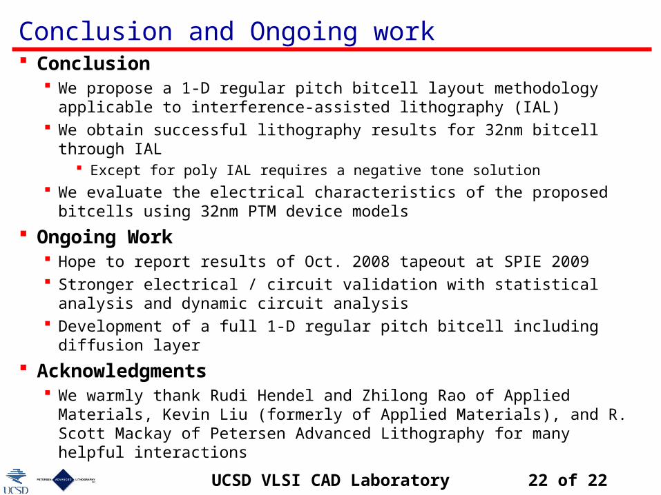
Electrical Metrics for Bitcell Design Rule of thumb of SRAM sizing
Cell ratio I(B) / I (C) ~ 2 Pull-up ratio I(A) / I (C) ~ 0.5
N-curve Static current/voltage noise margin Write trip current/voltage
Butterfly curve (Static Noise Margin) Voltage transfer curve
Iread
Measure bitline current going to bitcell during read mode
Ileakage
Measure power/ground current during stable state
VDDHOLD
Decreasing VDD, measure VDD when Vnr ~ Vnl
-1.0E-04
0.0E+00
0.00
0.07
0.14
0.21
0.28
0.35
0.42
0.49
0.56
0.63
0.70
0.77
0.84
0.91
0.98
WTV
SVNM
SINM
WTI
WTP
A1 A2
B1 B2
C1 C2 nl nr
VDD
WL
BLb BL
‘0’‘1’
= ‘1’
measure‘Iread’
‘1’ ‘1’
A1 A2
B1 B2
C1 C2 nl nr
VDD
WL
BLb BL
‘1’‘0’
= ‘0’
A1 A2
B1 B2
C1 C2 nl nr
VDD
WL
BLb BL

Taccess
Measure method Pre-charge bitlines Turn-on wordline Measure time at |VBL-VBLB| ~ 0.1VDD
Note Requires transient analysis Requires whole column configuration to calculate bitline capacitance Smaller is better
Taccess
A1 A2
B1 B2
C1 C2 nl nr
VDD
WL
BLb BL
‘1’‘0’
:‘0’ ‘1’
charge to ‘1’ charge to ‘1’
BL
BLB
WL
~0.1VDD
VLSICAD Lab., UCSD 35 of 24

Twrite
Measure Method Measure time when NL crosses the trip point
Note Requires transient analysis Smaller is better
A1 A2
B1 B2
C1 C2 nl nr
VDD
WL
BLb BL
‘0’‘1’
: ‘0’ ‘1’
‘0’ ‘1’ Twrite
WL
NL
Trip point
NR
VLSICAD Lab., UCSD 36 of 24

VREAD
Measure method Measure voltage of the low state node (e.g., nl) at the read condition
Note Shows read-stability Smaller is better
A1 A2
B1 B2
C1 C2 nl nr
VDD
WL
BLb BL
‘1’‘0’
‘1’
charge to ‘1’ charge to ‘1’
VLSICAD Lab., UCSD 37 of 24

VIA1: 90nm IL + CPA MASK
Black=Clear & no quartz etch
Blocking Mask
Image 1 formed with 4-beam interference
Green=Resist
VLSICAD Lab., UCSD 38 of 24

Metal2: 90nm IL + CPA Xquad 0.94/0.1
Black=Clear & no quartz etch
Blocking Mask
Green=Resist
VLSICAD Lab., UCSD 39 of 24

Metal3: 90nm IL + CPA Xquad 0.94/0.1
Black=Clear & no quartz etch
Blocking Mask
Green=Resist
VLSICAD Lab., UCSD 40 of 24

(Optional) IAL + DPL: 1-D Regular Active
Problem of 1-D Regular Active SRAM Combination of IAL and DPL Possible improvement of IAL-DPL SRAM
VLSICAD Lab., UCSD 41 of 24

Problem Description (1)
In the previous bitcell structures, IAL can not be applied to active (diffusion ) layer
It may require multiple processing to make such 2D active shapes by IAL, or it may be difficult to make sharp edge on the active layer by single exposure
S. Verhaegen et al.[6] presented that transistor’s “width” does not have much impact on the bitcell behavior
(a) Diffusion and NW
VLSICAD Lab., UCSD 42 of 24

Problem Description (2):1-D Regular Pitch Active We use the same width for all transistors Changing width from 15n to 100nm, we plot butterfly curve and N-
curve Compared to the original structure (cell ratio=2, in red solid lines),
SNM and N-curve are significantly degraded. 1-D regular pitch active bitcell seems infeasible
0.00E+00
2.00E-01
4.00E-01
6.00E-01
8.00E-01
1.00E+00
1.20E+00
0 0.2 0.4 0.6 0.8 1 1.2
15n
20n
25n
30n
35n
40n
45n
50n
55n
60n
65n
70n
75n
80n
85n
90n
95n
100n
2D: 25x12
-2.50E-04
-2.00E-04
-1.50E-04
-1.00E-04
-5.00E-05
0.00E+00
5.00E-05
1.00E-04
1 8 15 22 29 36 43 50 57 64 71 78 85 92 99
15n20n25n30n35n40n45n50n55n60n65n70n75n80n85n90n95n100n25x12
VLSICAD Lab., UCSD 43 of 24

Possible solution
To enhance SNM and N-curve metrics, cell ratio must be increased For fixed transistor width, cell ratio (PD/PG) can be improved by
changing gate length of PG PG and PD are in different polys, so they can have different gate
length if IAL is combined with double patterning Is this possible?
+Large Lgate
VLSICAD Lab., UCSD 44 of 24

(IL+PL)+(IL+PL) Process There are two types of HOMA; one is "single resist" and the other is "dual
resist". (Fritze et al., J. Vac. Sci. Tech. B 23(6), 2005) In the single resist process, IL makes grating patterns on the resist and then PL removes
unnecessary grating patterns (trim) on the same resist In the dual resist process, IL makes grating patterns on the first resist and then the wafer is
developed and baked. Second resist is coated on the remaining resist patterns and PL removes unnecessary patterns again
To make two different linewidths (g1 and g2) for the bitcell, g1 patterns can be generated by single resist process (IL+PL) After that, the wafer can be developed, baked and coated by the second resist After that, if we make g2 linewidth by using the same methodology (IL+PL) used for g1, Then we can get both g1 and g2 shape resist This can be thought as two successive sigle resist IAL with developing and baking steps
between the two single resist IAL processes Since to make the contact or via patterns, two IAL (vertical and horizontal)
and one PL process are required. So, compared with contact/via generation, IAL+DPL may requires one more process but it will allow diffusion to be generated by IAL
VLSICAD Lab., UCSD 45 of 24

Electrical Characteristics We use the same width (=88nm) for all transistors. Changing Lgate of PG from 33n to 50nm, we plot butterfly curve and N-curve. As increasing Lgate of PG, SNM is improved and becomes better than the
original (in red solid line, PG=PU=44n, PD=88nm, Lg=32nm for all) Around 40nm of Lg for PG, 1-D regular pitch active has similar SNM and N-curve of REF.
0.00E+00
2.00E-01
4.00E-01
6.00E-01
8.00E-01
1.00E+00
1.20E+00
0 0.2 0.4 0.6 0.8 1 1.2
33n
34n
35n
36n
37n
38n
39n
40n
41n
42n
43n
44n
45n
46n
47n
48n
49n
50n
REF
-2.50E-04
-2.00E-04
-1.50E-04
-1.00E-04
-5.00E-05
0.00E+00
5.00E-05
1.00E-04
1 9 17 25 33 41 49 57 65 73 81 89 97
33n34n35n36n37n38n39n40n41n42n43n44n45n46n47n48n49n50nREF
VLSICAD Lab., UCSD 46 of 24
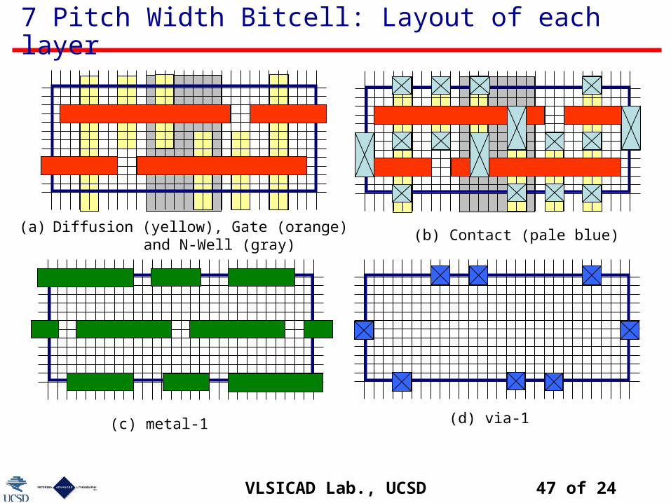
7 Pitch Width Bitcell: Layout of each layer
(a) Diffusion (yellow), Gate (orange) and N-Well (gray)
(b) Contact (pale blue)
(c) metal-1 (d) via-1
VLSICAD Lab., UCSD 47 of 24